WO2015098342A1 - 画像処理方法、画像処理装置、画像処理プログラム、及び画像処理プログラムを記憶した記憶媒体 - Google Patents
画像処理方法、画像処理装置、画像処理プログラム、及び画像処理プログラムを記憶した記憶媒体 Download PDFInfo
- Publication number
- WO2015098342A1 WO2015098342A1 PCT/JP2014/080093 JP2014080093W WO2015098342A1 WO 2015098342 A1 WO2015098342 A1 WO 2015098342A1 JP 2014080093 W JP2014080093 W JP 2014080093W WO 2015098342 A1 WO2015098342 A1 WO 2015098342A1
- Authority
- WO
- WIPO (PCT)
- Prior art keywords
- image
- pattern
- semiconductor device
- pattern image
- measurement
- Prior art date
- Legal status (The legal status is an assumption and is not a legal conclusion. Google has not performed a legal analysis and makes no representation as to the accuracy of the status listed.)
- Ceased
Links
Images




Classifications
-
- G—PHYSICS
- G06—COMPUTING OR CALCULATING; COUNTING
- G06T—IMAGE DATA PROCESSING OR GENERATION, IN GENERAL
- G06T7/00—Image analysis
- G06T7/0002—Inspection of images, e.g. flaw detection
- G06T7/0004—Industrial image inspection
-
- G—PHYSICS
- G06—COMPUTING OR CALCULATING; COUNTING
- G06T—IMAGE DATA PROCESSING OR GENERATION, IN GENERAL
- G06T7/00—Image analysis
- G06T7/0002—Inspection of images, e.g. flaw detection
- G06T7/0004—Industrial image inspection
- G06T7/001—Industrial image inspection using an image reference approach
-
- G—PHYSICS
- G06—COMPUTING OR CALCULATING; COUNTING
- G06F—ELECTRIC DIGITAL DATA PROCESSING
- G06F18/00—Pattern recognition
- G06F18/20—Analysing
- G06F18/22—Matching criteria, e.g. proximity measures
-
- G—PHYSICS
- G06—COMPUTING OR CALCULATING; COUNTING
- G06V—IMAGE OR VIDEO RECOGNITION OR UNDERSTANDING
- G06V10/00—Arrangements for image or video recognition or understanding
- G06V10/40—Extraction of image or video features
- G06V10/42—Global feature extraction by analysis of the whole pattern, e.g. using frequency domain transformations or autocorrelation
-
- G—PHYSICS
- G06—COMPUTING OR CALCULATING; COUNTING
- G06V—IMAGE OR VIDEO RECOGNITION OR UNDERSTANDING
- G06V10/00—Arrangements for image or video recognition or understanding
- G06V10/40—Extraction of image or video features
- G06V10/46—Descriptors for shape, contour or point-related descriptors, e.g. scale invariant feature transform [SIFT] or bags of words [BoW]; Salient regional features
-
- G—PHYSICS
- G06—COMPUTING OR CALCULATING; COUNTING
- G06V—IMAGE OR VIDEO RECOGNITION OR UNDERSTANDING
- G06V10/00—Arrangements for image or video recognition or understanding
- G06V10/70—Arrangements for image or video recognition or understanding using pattern recognition or machine learning
- G06V10/74—Image or video pattern matching; Proximity measures in feature spaces
- G06V10/75—Organisation of the matching processes, e.g. simultaneous or sequential comparisons of image or video features; Coarse-fine approaches, e.g. multi-scale approaches; using context analysis; Selection of dictionaries
-
- G—PHYSICS
- G06—COMPUTING OR CALCULATING; COUNTING
- G06T—IMAGE DATA PROCESSING OR GENERATION, IN GENERAL
- G06T2207/00—Indexing scheme for image analysis or image enhancement
- G06T2207/10—Image acquisition modality
- G06T2207/10048—Infrared image
-
- G—PHYSICS
- G06—COMPUTING OR CALCULATING; COUNTING
- G06T—IMAGE DATA PROCESSING OR GENERATION, IN GENERAL
- G06T2207/00—Indexing scheme for image analysis or image enhancement
- G06T2207/30—Subject of image; Context of image processing
- G06T2207/30108—Industrial image inspection
- G06T2207/30148—Semiconductor; IC; Wafer
Definitions
- the present invention relates to an image processing method, an image processing apparatus, and an image processing program.
- Patent Document 1 discloses a measuring device including a scanning electron microscope for measuring the line width of a circuit pattern formed on a semiconductor wafer. In this apparatus, position detection in an observation image is performed using a template.
- the accuracy of alignment between the pattern image and the signal image including the measurement image is important.
- the light emission image or the heat generation image of the inspection target device does not include the circuit pattern of the inspection target device.
- the heat generation image is a measurement image
- the heat generation image is located at the center of the measurement image.
- the present invention has been made in view of such problems, and an image processing method capable of accurately generating a superimposed image of a measurement image such as a light emission image or a heat generation image of a semiconductor device and a pattern image thereof.
- An object is to provide an image processing apparatus and an image processing program.
- an image processing method is a method for acquiring an image of a semiconductor device, the measurement image measured for the semiconductor device, and the semiconductor device corresponding to the measurement image
- an image processing apparatus is an apparatus for acquiring an image of a semiconductor device, and shows a measurement image measured for the semiconductor device and a pattern of the semiconductor device corresponding to the measurement image. Based on the first pattern image, the second pattern image indicating the pattern of the semiconductor device, the first pattern image, and the second pattern image based on the first pattern image and the second pattern image. An image analysis unit that acquires matching information indicating a relative relationship with the pattern image, and an image processing unit that acquires a superimposed image by superimposing the second pattern image and the measurement image based on the matching information. Prepare.
- an image processing program is a program for acquiring an image of a semiconductor device, the computer corresponding to a measurement image measured for the semiconductor device, and showing a pattern of the semiconductor device.
- An image analysis unit that obtains matching information indicating a relative relationship between the first pattern image and the second pattern image based on the first pattern image and the second pattern image indicating the pattern of the semiconductor device; and Based on the matching information, the second pattern image and the measurement image are superimposed to function as an image processing unit that acquires a superimposed image.
- image processing apparatus image processing program, or recording medium storing the image processing program, the first pattern image corresponding to the measurement image of the semiconductor device and the second pattern of the semiconductor device
- the positional relationship between the second pattern image and the measurement image can be obtained accurately based on matching information between the images, and a superimposed image of the second pattern image and the measurement image is acquired based on the positional relationship.
- a highly accurate superimposed image can be obtained.
- a measurement image such as a light emission image or a heat generation image of a semiconductor device and its pattern image.
- FIG. 1 is a schematic configuration diagram of an observation system 1A that is an image processing apparatus according to a first embodiment of the present invention. It is a figure which shows an example of the image of the measurement image memorize
- FIG. 1 is a schematic configuration diagram of an observation system 1A that is an image processing apparatus according to a first embodiment of the present invention.
- An observation system 1A shown in FIG. 1 is an optical system that acquires and processes an image in order to observe a heat generation image of a semiconductor device such as an IC (integrated circuit) such as a semiconductor memory or LSI, or a power device.
- This observation system 1A includes an infrared camera 3, a two-dimensional camera 5, an illumination device 7, a dichroic mirror 9, a beam splitter 11 such as a half mirror, an objective lens 13, a stage 15, a computer (Personal Computer) 17, a tester 19, and an input.
- a device 21 and a display device 23 are included.
- the infrared camera 3 is an imaging device such as an InSb (indium antimony) camera having sensitivity to infrared wavelengths, and acquires a measurement image by capturing a heat generation image of the semiconductor device S placed on the stage 15.
- the infrared camera 3 detects a heat generation image of the semiconductor device S placed on the stage 15 via the objective lens 13 and the dichroic mirror 9.
- the two-dimensional camera 5 is a camera incorporating a CCD (Charge-Coupled Device) image sensor, a CMOS (Complementary Metal-Oxide Semiconductor) image sensor, and the like, and a pattern image showing a pattern of the semiconductor device S mounted on the stage 15. A two-dimensional image is taken.
- the two-dimensional camera 5 detects a two-dimensional image of the semiconductor device via the objective lens 13, the dichroic mirror 9 and the beam splitter 11.
- the objective lens 13 is provided facing the semiconductor device S and sets the magnification of the image formed on the infrared camera 3 and the two-dimensional camera 5.
- the objective lens 13 includes an objective lens switching unit 25 and a plurality of lenses having different magnifications.
- the objective lens 13 that connects an image to the infrared camera 3 or the two-dimensional camera 5 is replaced with a high-power lens and a low-power lens. The function to switch between.
- the dichroic mirror 9 transmits infrared light to guide the heat generation image of the semiconductor device S to the infrared camera 3, and infrared to guide the pattern image of the semiconductor device S to the two-dimensional camera 5. Reflects light of wavelengths other than the wavelength.
- the beam splitter 11 transmits the pattern image reflected by the dichroic mirror 9 toward the two-dimensional camera 5 and reflects the illumination light for generating the pattern image emitted from the illumination device 7 toward the dichroic mirror 9.
- the semiconductor device S is irradiated with the illumination light via the dichroic mirror 9 and the objective lens 13.
- the tester 19 applies a test pattern of a predetermined electric signal, a predetermined voltage, or a predetermined current to the semiconductor device S. By applying the test pattern, a heat generation image due to the failure of the semiconductor device S is generated.
- the computer 17 is an image processing apparatus that processes images acquired by the infrared camera 3 and the two-dimensional camera 5. Specifically, the computer 17 includes a storage unit 27, an image analysis unit 29, an image processing unit 31, and a control unit 33 as functional components. Further, the computer 17 is provided with an input device 21 such as a mouse and a keyboard for inputting data to the computer 17 and a display device 23 such as a display device for displaying an image processing result by the computer 17. .
- Each functional unit of the computer 17 shown in FIG. 1 is executed by an arithmetic processing unit such as a CPU of the computer 17 executing a computer program (image processing program) stored in a storage medium such as a built-in memory or a hard disk drive of the computer 17.
- arithmetic processing unit of the computer 17 causes the computer 17 to function as each function unit of FIG. 1 by executing this computer program, and sequentially executes processing corresponding to an image processing method to be described later.
- Various data necessary for the execution of the computer program and various data generated by the execution of the computer program are all stored in a storage medium such as a built-in memory such as ROM or RAM of the computer 17 or a hard disk drive.
- the storage unit 27 is a measurement image in which a heat generation image acquired by the infrared camera 3 is detected, a first pattern image in which a pattern image of the semiconductor device S acquired by the infrared camera 3 is detected, and the two-dimensional camera 5.
- the second pattern image in which the pattern image of the semiconductor device acquired by the above is detected is sequentially stored.
- the image analysis unit 29 and the image processing unit 31 perform various types of image data processing on the image stored in the storage unit 27. Specifically, the image analysis unit 29 acquires matching information indicating a relative relationship regarding the position, size, and angle between the first pattern image and the second pattern image stored in the storage unit 27.
- the image processing unit 31 acquires a superimposed image by superimposing the second pattern image and the heat generation image in the measurement image while referring to the matching information acquired by the image analysis unit 29.
- the control unit 33 controls data processing in the computer 17 and processing of devices connected to the computer 17. For example, the control unit 33 emits illumination light by the illumination device 7, captures images by the infrared camera 3 and the two-dimensional camera 5, switches the magnification of the objective lens 13, applies a test pattern by the tester 19, and observes results by the display device 23. Controls display of (superimposed image, etc.).
- the computer 17 receives an instruction to start the observation process of the semiconductor device from the operator of the observation system 1A using the input device 21, the magnification of the objective lens 13 set in advance by the control of the control unit 33 ( For example, application of a test pattern by the tester 19 is started after switching to low magnification.
- a measurement image including a heat generation image of the semiconductor device is acquired by the infrared camera 3 and stored in the storage unit 27 (step A1-1: heat generation image acquisition step).
- the measurement image is generated by adding a plurality of pieces of image data continuously captured with a predetermined exposure time.
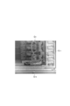
- FIG. 2 shows an example of the measurement image stored in the storage unit 27.
- the measurement image G 1 include the pattern image G 11 due to the heat from the entire semiconductor device S is imaged, fever image G 12 emitted with the application of the test pattern from the observation target portion, such as a failure site It is.
- the pattern image G 11 is an image representing a pattern of a semiconductor device S.
- the first pattern image including only the pattern image of the semiconductor device is acquired by the infrared camera 3 and stored in the storage unit 27 (step A1-2: pattern image acquisition step).
- the first pattern image is generated by adding a plurality of pieces of image data continuously captured with a predetermined exposure time, as in step A1-1.
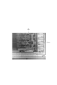
- FIG. 3 shows an example of the image of the first pattern image stored in the storage unit 27.
- the first pattern image G 2 includes only a pattern image G 11 obtained by capturing heat from the entire semiconductor device S.
- the pattern image G 11 is an image representing the pattern of the semiconductor device S. That is, the first pattern image G 2 is, to match the pattern image included in the measurement image G 1 a represents the (corresponding) pattern image.
- the image analysis unit 29 of the computer 17, from the storage unit 27 reads the measurement image G 1 and the first pattern image G 2, by the measurement image G 1 to the first pattern image G 2 to differential processing, only the heat generating image the measurement image G 1 including a processing and generating (step A1-3: fever image difference step).
- FIG 4 shows an example of the image measurement image G 1 generated by the image analysis unit 29. Thus, only the heat generating image G 12 and pattern image is removed from the measurement image G 1 is appearing.
- step A2 heat generation image acquisition step.
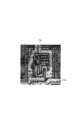
- FIG. 5 shows an example of an image of the second pattern image stored in the storage unit 27.
- This second pattern image G 3 reflected light from the entire semiconductor device S is included pattern image G 31 by being imaged. Reflection images from the entire semiconductor device, because it shows a surface shape for forming a semiconductor device, the pattern image G 31 is an image showing the surface pattern of the semiconductor device S.
- step A3 matching information obtaining step
- step A3 firstly, a field size in the size range of the semiconductor device S of the first pattern image G 2, and field size in the size range of the second semiconductor device of the pattern image G 3 S based on the ratio, adjusting at least one of the image size of the first pattern image G 2 or the second pattern image G 3 (step A3-1: pattern image adjustment step). More specifically, the image analysis unit 29 obtains the magnification of the first pattern image G 2 magnification of the objective lens 13 when obtaining the second pattern image G 3 objective lens 13 when acquiring the, each inverse to a numerical value showing the viewing size of the first pattern image G 2, and the second pattern image G 3.
- the image analysis unit 29 adjusts on the basis of those numbers to fit the size of the second pattern image G 3 to the image size on the first pattern image G 2. For example, magnification 15 times the time of the acquisition of the first pattern image G 2, when the magnification when obtaining the second pattern image G 3 is 100 times, each of the field size 1/15, 1/100 and then to adjust the image size of the second pattern image G 3 in 15/100 times.
- the image analysis unit 29 may adjust the image size of the first pattern image G 2 or both. May be adjusted to another image size of the same magnification.
- Step A3-2 shape-based matching step.
- the image analysis unit 29, the first pattern image G 2, and the second pattern image G 3 extracts the respective outline (edge line) as the first and second shape information.
- the image analysis unit 29 searches for similar patterns that are similar to each other between the first shape information and the second shape information.
- Figure 6 shows an example of a second shape information by the image analysis unit 29 extracted from the second pattern image G 3.
- the contour of the pattern image G 31 in the second pattern image G 3 is extracted as a second shape information P 3.
- the image analysis unit 29 performs matching at a pyramid level by changing the resolution of one or both of the first pattern image G 2 and the second pattern image G 3 to a plurality of layers. . That is, when acquiring both the first pattern image G 2 and the second pattern image G 3 or one of the low resolution images at a plurality of resolutions and matching the first pattern image G 2 and the second pattern image G 3 , The shape matching process with the other image is sequentially advanced from the low-resolution high-level image to the high-resolution low-level image. Thereby, high-speed matching processing is realized.
- the image analysis unit 29, according to the resolution of the first pattern image G 2, and the second pattern image G 3 contrast and the original image may be set number of layers of the pyramid.
- Step A3-3 information acquiring step.
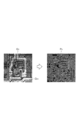
- FIG. 7 shows an example of the second shape information P 3 of the first pattern image G 2 and the second pattern image G 3 to be subjected to matching processing by the image analysis unit 29. As shown in the figure, from the first matching pattern image G 2 results for the second shape information P 3, matching information is acquired.
- step A4 superimposed image acquisition step.
- Figure 8 is the image processing unit 31 withdrawn from the measurement image G 1, it shows an example of the extracted image G 13 including a heating image G 12. Then, the image processing unit 31, extracts the image G 13 and the second pattern image G 3 and is superimposed on the superimposed image G 4 is generated.
- the extracted image G 13 withdrawn from the measurement image G 1 is the image processing unit 31, the interpolation processing of pixel is performed so that the second pattern image G 3 and resolution match.
- FIG 9 shows an example of the extracted image G 13 and the second pattern image G 3 and is superimposed on the basis of the superimposed image G 4 by the image processing unit 31.
- a second pattern image G 3 of the semiconductor device S The positional relationship between the second pattern image G 3 and the measurement image G 1 can be obtained with high accuracy based on the matching information of the second pattern image G 3 , and the superimposed image G of the second pattern image G 3 and the measurement image G 1 based on the positional relationship.
- shape information is extracted from each of the first and second pattern images G 2 and G 3 , and matching information is acquired based on the shape information.
- the first and second pattern image G 2 even if the contrast of G 3 is different to easily obtain matching information.
- At least one of the image size of the first and second pattern image G 2, G 3 is adjusted. In this case, even field size are different measurement image G 1 and the second pattern image G 3, it is possible to create a superimposed image G 4 position on the semiconductor device S of both of the images are matched.
- position information, rotation information, and magnification information indicating the relative relationship between the first and second pattern images G 2 and G 3 are used as matching information.
- the measurement image G 1 and the positional relationship between the second pattern image G 2 can be obtained easily, which can be acquired superimposed image G 4 easily based.
- FIG. 10 is a schematic configuration diagram of an observation system 1B according to a first modification of the first embodiment of the present invention.
- the measurement image G 1 is acquired as a luminescent image of the semiconductor device S.
- the infrared camera 3 is removed as compared with the observation system 1A, and a mirror 9B is provided instead of the dichroic mirror 9.
- a test pattern is applied by the tester 19 and the sensitivity of the two-dimensional camera 5 is set to a high gain.
- luminescent image is acquired as the measurement image G 1.
- the illumination device 7 emits illumination light
- the tester 19 stops applying the test pattern
- the two-dimensional camera 5 reflects the semiconductor device S in a state where the sensitivity of the two-dimensional camera 5 is set to a low gain.
- the first pattern differential processing image G 2 from the measurement image G 1 is not necessarily required. Further, at the time of acquisition first pattern image G 2 test patterns may remain applied. Also, imaging the luminescent image reflected by the mirror 9B to remove the beam splitter 11 at the time of acquisition of the measurement image G 1 directly in a two-dimensional camera 5, at the time of acquisition first pattern image G 2 is attached to the beam splitter 11 mirror 9B The reflection image reflected by the beam may be taken by the two-dimensional camera 5 through the beam splitter 11. In this case, a mirror may be used instead of the beam splitter 11.
- the two-dimensional camera 5 may be an InGaAs camera or an MCT (Mercury Cadmium Tellu) camera in addition to a camera incorporating a CCD image sensor or a CMOS image sensor having sensitivity to near infrared wavelengths.
- MCT Mercury Cadmium Tellu
- FIG. 11 is a schematic configuration diagram of an observation system 1C according to the second modification of the first embodiment of the present invention.
- the configuration related to the acquisition of the measurement image and the first pattern image is shown, and the configuration related to the acquisition of the second pattern image is the same as that of the first embodiment, and is not shown.
- the measurement image G 1 is acquired as an electrical signal an image of the semiconductor device S.
- the infrared camera 3 is removed, and a laser light source 7C that irradiates laser light is provided instead of the illumination device 7, and the two-dimensional camera 5 is replaced.
- a photodetector 3C such as a photodiode or avalanche photodiode for detecting the laser light reflected by the semiconductor device S, and a laser that scans the semiconductor device S two-dimensionally with the laser light instead of the dichroic mirror 9.
- Scanning means 9C is provided.
- the observation system 1C is provided with a power source 35 for applying an electric signal having a constant voltage or a constant current to the semiconductor device S, and an electric signal detecting means 19C electrically connected to the semiconductor device S. .
- Examples of such an electric signal image include an OBIC (Optical Beam Induced Current) image that is a photovoltaic current image, an OBIRCH (Optical Beam Induced Resistance Change) image that is an electric quantity change image, and an SDL (Soft Defect Localization) that is an error information image. ) Images.
- OBIC Optical Beam Induced Current
- OBIRCH Optical Beam Induced Resistance Change
- SDL Soft Defect Localization
- the OBIC image is obtained by detecting the photocurrent generated by the laser light as a characteristic value (current value or current change value) of an electric signal and imaging the characteristic value in association with laser irradiation position information. It is. Further, the OBIRCH image is obtained by scanning the laser beam with a constant current applied to the semiconductor device S, thereby changing the characteristic value (voltage value or voltage value) of the electric signal due to the change in the resistance value of the laser beam irradiation position of the semiconductor device S. (Change value of voltage) is imaged. That is, the OBIRCH image is an image formed by associating the voltage change value with the laser irradiation position information.
- the OBIRCH image is obtained by imaging the current change value of the electric signal due to the change in the resistance value of the irradiation position of the laser light of the semiconductor device S by scanning the laser light with a constant voltage applied to the semiconductor device S. It may be what you did.
- the SDL image is also called a DALS (Dynamic Analysis by Laser Laser Simulation) image or an LADA (Laser Assisted Device Alteration) image, and detects a malfunction state by scanning a laser beam with a test pattern applied to the semiconductor device S.
- DALS Dynamic Analysis by Laser Laser Simulation
- LADA Laser Assisted Device Alteration
- first pattern image G 2 which is stored.
- FIG. 12 is a schematic configuration diagram of an observation system 1D according to a third modification of the first embodiment of the present invention.
- the configuration related to the acquisition of the measurement image and the first pattern image is shown, and the configuration related to the acquisition of the second pattern image is the same as that of the first embodiment, and is not shown.
- the measurement image G 1 is being acquired as an electro-optical frequency mapping image of the semiconductor device S.
- the observation system 1D is provided with a laser light source 7C for irradiating a laser beam instead of the illuminating device 7 in place of the two-dimensional camera 5 in comparison with the observation system 1A.
- a photodetector 3C such as a photodiode or avalanche photodiode for detecting the laser light reflected by the semiconductor device S, and a laser that scans the semiconductor device S two-dimensionally with the laser light instead of the dichroic mirror 9. Scanning means 9C is provided.
- a test pattern is repeatedly applied to the semiconductor device S by the tester 19, and the laser light emitted from the laser light source 7C is scanned two-dimensionally on the semiconductor device S by the laser scanning unit 9C.
- the reflected light generated in the semiconductor device S is detected by the photodetector 3C.
- the frequency analysis device 4 such as a spectrum analyzer or a lock-in detector.
- the frequency analysis device 4 performs frequency analysis at a specific frequency on the detection signal and outputs analysis data to the computer 17.
- the scanning position of the laser beam on the semiconductor device S and the analysis data are associated with each other, and an electro-optic frequency mapping image (EOFM (Electro Optical Frequency Mapping) obtained by imaging the signal intensity of the part operating at a specific frequency. ) image) is stored as a measurement image G 1 in the storage unit 27.
- the electro-optic frequency mapping image is an amplitude image, a phase image, an I / Q image, or the like.
- the analysis data is the amplitude of the detection signal at a specific frequency
- the analysis data is the phase (phase difference) between the signal of the specific frequency and the detection signal.
- the analysis data is an I / Q value (In-phase / Quadrature value) indicating a change in amplitude and phase.
- the DC component of the detection signal of the photodetector 3C is extracted, and the first pattern image G in which the scanning position of the laser light on the semiconductor device S and the DC component of the detection signal are associated and imaged in the storage unit 27 is extracted. 2 is stored.
- the modulated light of the reflected light generated along with the operation of an element such as a transistor when the semiconductor device S is irradiated with the laser light is observed as two-dimensional image information.
- this invention is not limited to embodiment mentioned above.
- multi-photon absorption such as two-photon absorption is caused by irradiating the semiconductor device S with a short pulse laser such as a femtosecond laser having a wavelength of 1200 nm or more.
- a photocurrent image MOBIC image
- the second pattern image G 3 using the CAD layout data of the semiconductor device S, it may be superimposed measuring image on the CAD layout data.
- the second pattern image G 3 or may be a transmission image of the captured transmitted image such as an X-ray.
- a light source that outputs highly coherent light such as an LED (Light Emitting Diode) light source as well as the laser light source may be adopted.
- a light source that outputs low-coherence light (incoherent light) such as an SLD (Super Luminescent Diode) light source, an ASE (Amplified Spontaneous Emission) light source, or a lamp light source may be used.
- the laser light source 7C outputs light having a wavelength that causes multiphoton absorption in the semiconductor device S (for example, a wavelength of 1200 nm or more) and a short pulse width (for example, a pulse width such as sub-picosecond or femtosecond). It may be a light source.
- the measurement image G 1 of the semiconductor device S, the first to obtain the pattern image G 2 device and the semiconductor device S device to obtain a second pattern image G 3 showing a pattern of a semiconductor device corresponding to the measurement image G 1 may be a separate device may be integral, also acquisition of the measurement image G 1 and the first pattern image G 2, acquisition of the second pattern image G 3 are not performed in the flow of a series of processes May be.
- the measurement image G 1 , the first pattern image G 2 from which the pattern image of the semiconductor device S is detected, and the second pattern image G 3 from which the pattern image of the semiconductor device S is detected are stored in the storage unit of the computer 17. 27, since the image analysis unit 29 and the image processing unit 31 perform various types of image data processing on the image stored in the storage unit 27, there are limitations on the apparatus, measurement environment, and measurement flow. Hateful.
- the matching information and second pattern image G 3 based on the third pattern image corresponding to the second measurement image and the second measurement image the 2 pattern measurement image G 1 and the second measurement image in the image G 3 may be superimposed to.
- the second pattern image G 3 analysis of the semiconductor device S is easily performed based on the plurality of measurement images.
- the first shape information is extracted from the first pattern image
- the second pattern image is extracted from the second pattern image.
- the shape information of 2 may be extracted, and the matching information may be acquired based on the first shape information and the second shape information. In this way, matching information can be easily obtained even when the contrast between the first pattern image and the second pattern image is different.
- a first field size indicating a range on the semiconductor device of the first pattern image and a second field size indicating the range on the semiconductor device of the second pattern image may be adjusted based on the ratio. In this case, even if the visual field sizes of the measurement image and the second pattern image are different, it is possible to create a superimposed image in which the positions of the images on the semiconductor device match.
- the matching information may be at least one of position information indicating the relative relationship between the first pattern image and the second pattern image, rotation information, and magnification information. If such matching information is used, the positional relationship between the measurement image and the second pattern image can be easily obtained, and a superimposed image can be easily obtained based on this.
- the measurement image may be at least one of a heat generation image, a light emission image, an electric quantity change image, a photocurrent image, a correct / incorrect information image, a phase image, an amplitude image, and an I / Q image of the semiconductor device.
- the second pattern image may be any of a reflection image, a transmission image, a MOBIC image, and a CAD layout image of the semiconductor device.
- the present invention uses an image processing method, an image processing apparatus, and an image processing program, and can accurately generate a superimposed image of a measurement image such as a light emission image or a heat generation image of a semiconductor device and its pattern image. It is.
Landscapes
- Engineering & Computer Science (AREA)
- Theoretical Computer Science (AREA)
- Computer Vision & Pattern Recognition (AREA)
- General Physics & Mathematics (AREA)
- Physics & Mathematics (AREA)
- Multimedia (AREA)
- Evolutionary Computation (AREA)
- Artificial Intelligence (AREA)
- Data Mining & Analysis (AREA)
- Quality & Reliability (AREA)
- Life Sciences & Earth Sciences (AREA)
- Bioinformatics & Computational Biology (AREA)
- Databases & Information Systems (AREA)
- Health & Medical Sciences (AREA)
- Software Systems (AREA)
- General Health & Medical Sciences (AREA)
- Bioinformatics & Cheminformatics (AREA)
- Computing Systems (AREA)
- Evolutionary Biology (AREA)
- General Engineering & Computer Science (AREA)
- Medical Informatics (AREA)
- Testing Or Measuring Of Semiconductors Or The Like (AREA)
- Image Processing (AREA)
- Image Analysis (AREA)
- Investigating Materials By The Use Of Optical Means Adapted For Particular Applications (AREA)
- Length Measuring Devices By Optical Means (AREA)
Abstract
Description
Claims (9)
- 半導体デバイスを対象に測定された測定画像と、前記測定画像に対応する前記半導体デバイスのパターンを示す第1のパターン画像を取得する第1ステップと、
前記半導体デバイスのパターンを示す第2のパターン画像を取得する第2ステップと、
前記第1のパターン画像と前記第2のパターン画像とに基づいて、前記第1のパターン画像と前記第2のパターン画像との相対関係を示すマッチング情報を取得する第3ステップと、
前記マッチング情報を基に、前記第2のパターン画像と前記測定画像とを重畳することによって重畳画像を取得する第4ステップと、
を備えることを特徴とする画像処理方法。 - 前記第3ステップでは、前記第1のパターン画像から第1の形状情報を抽出し、前記第2のパターン画像から第2の形状情報を抽出し、前記第1の形状情報及び前記第2の形状情報を基にマッチング情報を取得する、
ことを特徴とする請求項1記載の画像処理方法。 - 前記第3ステップでは、前記第1のパターン画像の前記半導体デバイス上の範囲を示す第1の視野サイズと、前記第2のパターン画像の前記半導体デバイス上の範囲を示す第2の視野サイズとの比に基づいて、前記第1のパターン画像及び前記第2のパターン画像の少なくともいずれか一方の画像サイズを調整する、
ことを特徴とする請求項1又は2記載の画像処理方法。 - 前記マッチング情報は、前記第1のパターン画像と前記第2のパターン画像との相対関係を示す位置情報、回転情報、及び倍率情報の少なくとも1つである、
ことを特徴とする請求項1~3のいずれか1項に記載の画像処理方法。 - 前記測定画像は、前記半導体デバイスの発熱画像、発光画像、電気量変化画像、光起電流画像、正誤情報画像、位相画像、振幅画像及びI/Q画像のうちの少なくとも1つである、
ことを特徴とする請求項1~4のいずれか1項に記載の画像処理方法。 - 前記第2のパターン画像は、半導体デバイスの反射画像、透過画像、MOBIC画像、及びCADレイアウト画像のうちのいずれかである、
ことを特徴とする請求項1~5のいずれか1項に記載の画像処理方法。 - 半導体デバイスを対象に測定された測定画像と、前記測定画像に対応する前記半導体デバイスのパターンを示す第1のパターン画像と、前記半導体デバイスのパターンを示す第2のパターン画像とを記憶する記憶部と、
前記第1のパターン画像と前記第2のパターン画像とに基づいて、前記第1のパターン画像と前記第2のパターン画像との相対関係を示すマッチング情報を取得する画像解析部と、
前記マッチング情報を基に、前記第2のパターン画像と前記測定画像とを重畳することによって重畳画像を取得する画像処理部と、
を備えることを特徴とする画像処理装置。 - コンピュータを、
半導体デバイスを対象に測定された測定画像に対応し、前記半導体デバイスのパターンを示す第1のパターン画像と、前記半導体デバイスのパターンを示す第2のパターン画像とに基づいて、前記第1のパターン画像と前記第2のパターン画像との相対関係を示すマッチング情報を取得する画像解析部、及び
前記マッチング情報を基に、前記第2のパターン画像と前記測定画像とを重畳することによって重畳画像を取得する画像処理部、
として機能させることを特徴とする画像処理プログラム。 - 請求項8記載の画像処理プログラムを記憶した記憶媒体。
Priority Applications (4)
| Application Number | Priority Date | Filing Date | Title |
|---|---|---|---|
| KR1020167015055A KR102278352B1 (ko) | 2013-12-26 | 2014-11-13 | 화상 처리 방법, 화상 처리 장치, 화상 처리 프로그램 및 화상 처리 프로그램을 기억한 기억 매체 |
| SG11201602201XA SG11201602201XA (en) | 2013-12-26 | 2014-11-13 | Image processing method, image processing system, image processing program, and storage medium storing image processing program |
| JP2015554669A JP6679310B2 (ja) | 2013-12-26 | 2014-11-13 | 画像処理方法、画像処理装置、画像処理プログラム、及び画像処理プログラムを記憶した記憶媒体 |
| CN201480070586.7A CN105849883B (zh) | 2013-12-26 | 2014-11-13 | 图像处理方法、图像处理装置、图像处理程序及存储有图像处理程序的存储介质 |
Applications Claiming Priority (2)
| Application Number | Priority Date | Filing Date | Title |
|---|---|---|---|
| US201361920820P | 2013-12-26 | 2013-12-26 | |
| US61/920820 | 2013-12-26 |
Publications (1)
| Publication Number | Publication Date |
|---|---|
| WO2015098342A1 true WO2015098342A1 (ja) | 2015-07-02 |
Family
ID=53478218
Family Applications (2)
| Application Number | Title | Priority Date | Filing Date |
|---|---|---|---|
| PCT/JP2014/080096 Ceased WO2015098343A1 (ja) | 2013-12-26 | 2014-11-13 | 画像処理方法、画像処理装置、画像処理プログラム、及び画像処理プログラムを記憶した記憶媒体 |
| PCT/JP2014/080093 Ceased WO2015098342A1 (ja) | 2013-12-26 | 2014-11-13 | 画像処理方法、画像処理装置、画像処理プログラム、及び画像処理プログラムを記憶した記憶媒体 |
Family Applications Before (1)
| Application Number | Title | Priority Date | Filing Date |
|---|---|---|---|
| PCT/JP2014/080096 Ceased WO2015098343A1 (ja) | 2013-12-26 | 2014-11-13 | 画像処理方法、画像処理装置、画像処理プログラム、及び画像処理プログラムを記憶した記憶媒体 |
Country Status (7)
| Country | Link |
|---|---|
| US (2) | US9536300B2 (ja) |
| JP (4) | JP6679310B2 (ja) |
| KR (2) | KR102278352B1 (ja) |
| CN (2) | CN105849883B (ja) |
| SG (1) | SG11201602201XA (ja) |
| TW (2) | TWI634603B (ja) |
| WO (2) | WO2015098343A1 (ja) |
Cited By (5)
| Publication number | Priority date | Publication date | Assignee | Title |
|---|---|---|---|---|
| WO2020246150A1 (ja) | 2019-06-03 | 2020-12-10 | 浜松ホトニクス株式会社 | 半導体検査方法及び半導体検査装置 |
| WO2020246149A1 (ja) | 2019-06-03 | 2020-12-10 | 浜松ホトニクス株式会社 | 半導体検査装置及び半導体検査方法 |
| WO2021250984A1 (ja) | 2020-06-08 | 2021-12-16 | 浜松ホトニクス株式会社 | 半導体検査方法及び半導体検査装置 |
| JP2024522595A (ja) * | 2021-06-08 | 2024-06-21 | バテル メモリアル インスティチュート | 微小電子デバイスの高分解能結像 |
| US12340504B2 (en) | 2020-06-08 | 2025-06-24 | Hamamatsu Photonics K.K. | Semiconductor inspecting method and semiconductor inspecting device |
Families Citing this family (10)
| Publication number | Priority date | Publication date | Assignee | Title |
|---|---|---|---|---|
| KR101755518B1 (ko) | 2016-08-12 | 2017-07-07 | 현대자동차 주식회사 | 압축기 제어 장치 및 방법 |
| US10147178B2 (en) * | 2017-01-12 | 2018-12-04 | Nanya Technology Corporation | Method of recognizing wafer |
| JP2018128401A (ja) * | 2017-02-10 | 2018-08-16 | 東芝Itコントロールシステム株式会社 | X線透視検査装置 |
| JP6871070B2 (ja) * | 2017-06-06 | 2021-05-12 | 浜松ホトニクス株式会社 | 半導体デバイス検査方法 |
| TWI637352B (zh) * | 2017-08-23 | 2018-10-01 | 緯創資通股份有限公司 | 影像處理裝置和方法 |
| JP6898211B2 (ja) | 2017-11-27 | 2021-07-07 | 浜松ホトニクス株式会社 | 光計測方法、光計測装置、光計測プログラム、及び光計測プログラムを記録する記録媒体 |
| CN111417860B (zh) * | 2017-11-27 | 2023-04-07 | 浜松光子学株式会社 | 解析方法、解析装置、解析程序以及记录解析程序的存储介质 |
| US12105858B2 (en) * | 2020-03-11 | 2024-10-01 | University Of Florida Research Foundation, Incorporated | Systems and methods for laser probing for hardware trojan detection |
| TWI792621B (zh) * | 2021-10-20 | 2023-02-11 | 財團法人工業技術研究院 | 量測方法 |
| JP7565659B1 (ja) * | 2024-06-07 | 2024-10-11 | 不二越機械工業株式会社 | エッジ形状測定装置、及びエッジ形状測定方法 |
Citations (2)
| Publication number | Priority date | Publication date | Assignee | Title |
|---|---|---|---|---|
| JPH07311168A (ja) * | 1994-05-17 | 1995-11-28 | Hamamatsu Photonics Kk | 内部発熱解析装置 |
| WO2006137415A1 (ja) * | 2005-06-22 | 2006-12-28 | Hamamatsu Photonics K.K. | 半導体不良解析装置、不良解析方法、不良解析プログラム、及び不良解析システム |
Family Cites Families (22)
| Publication number | Priority date | Publication date | Assignee | Title |
|---|---|---|---|---|
| JPH02198347A (ja) * | 1989-01-27 | 1990-08-06 | Hitachi Ltd | 半導体不良解析装置 |
| JP2956658B2 (ja) * | 1997-06-26 | 1999-10-04 | 日本電気株式会社 | Lsiの異常発光箇所特定方法およびその装置 |
| JP4279412B2 (ja) * | 1999-07-07 | 2009-06-17 | 浜松ホトニクス株式会社 | 半導体デバイス検査装置 |
| JP3927353B2 (ja) * | 2000-06-15 | 2007-06-06 | 株式会社日立製作所 | 比較検査における画像の位置合せ方法、比較検査方法及び比較検査装置 |
| JP4154156B2 (ja) * | 2002-02-08 | 2008-09-24 | ソニーマニュファクチュアリングシステムズ株式会社 | 欠陥分類検査装置 |
| JP2004146428A (ja) * | 2002-10-22 | 2004-05-20 | Renesas Technology Corp | 故障解析方法 |
| JP4847685B2 (ja) | 2004-04-16 | 2011-12-28 | 株式会社日立ハイテクノロジーズ | パターンサーチ方法 |
| AU2005272460B2 (en) * | 2004-08-12 | 2012-03-22 | Nikon Corporation | Substrate Processing System, Method Of Confirmation Of Its State Of Use, And Method Of Prevention Of Illicit Use |
| JP4617970B2 (ja) * | 2005-04-01 | 2011-01-26 | ソニー株式会社 | 欠陥検査装置及び欠陥検査方法 |
| JP4450776B2 (ja) * | 2005-07-22 | 2010-04-14 | 株式会社日立ハイテクノロジーズ | 欠陥検査方法及び外観検査装置 |
| JP4791998B2 (ja) * | 2006-04-12 | 2011-10-12 | 株式会社東芝 | パターン形状評価方法およびプログラム |
| JP4943304B2 (ja) * | 2006-12-05 | 2012-05-30 | 株式会社 Ngr | パターン検査装置および方法 |
| JP5408852B2 (ja) * | 2007-08-09 | 2014-02-05 | 株式会社日立ハイテクノロジーズ | パターン測定装置 |
| JP2010177500A (ja) * | 2009-01-30 | 2010-08-12 | Hitachi High-Technologies Corp | パターンの重ね合わせ評価方法 |
| NL2004539A (en) * | 2009-06-22 | 2010-12-23 | Asml Netherlands Bv | Object inspection systems and methods. |
| JP5604067B2 (ja) * | 2009-07-31 | 2014-10-08 | 株式会社日立ハイテクノロジーズ | マッチング用テンプレートの作成方法、及びテンプレート作成装置 |
| SG178412A1 (en) * | 2009-08-17 | 2012-04-27 | Nanda Technologies Gmbh | Method of inspecting and processing semiconductor wafers |
| JP5556274B2 (ja) * | 2010-03-17 | 2014-07-23 | 凸版印刷株式会社 | パターン評価方法及びパターン評価装置 |
| JP5221584B2 (ja) * | 2010-03-25 | 2013-06-26 | 株式会社日立ハイテクノロジーズ | 画像処理装置、画像処理方法、画像処理プログラム |
| JP2013174823A (ja) * | 2012-02-27 | 2013-09-05 | Olympus Corp | 画像処理装置、顕微鏡システム、及び画像処理方法 |
| TW201339572A (zh) * | 2012-03-21 | 2013-10-01 | Optivu Vision System Corp | 元件內部缺陷之檢測裝置及方法 |
| JP5953117B2 (ja) * | 2012-05-21 | 2016-07-20 | 株式会社日立ハイテクノロジーズ | パターン評価装置、及びコンピュータープログラム |
-
2014
- 2014-11-13 CN CN201480070586.7A patent/CN105849883B/zh active Active
- 2014-11-13 KR KR1020167015055A patent/KR102278352B1/ko active Active
- 2014-11-13 WO PCT/JP2014/080096 patent/WO2015098343A1/ja not_active Ceased
- 2014-11-13 JP JP2015554669A patent/JP6679310B2/ja active Active
- 2014-11-13 KR KR1020167015056A patent/KR102278964B1/ko active Active
- 2014-11-13 WO PCT/JP2014/080093 patent/WO2015098342A1/ja not_active Ceased
- 2014-11-13 CN CN201480070583.3A patent/CN105849882B/zh active Active
- 2014-11-13 SG SG11201602201XA patent/SG11201602201XA/en unknown
- 2014-11-13 JP JP2015554670A patent/JP6456301B2/ja active Active
- 2014-12-10 TW TW103143114A patent/TWI634603B/zh active
- 2014-12-10 TW TW103143119A patent/TWI626601B/zh active
- 2014-12-24 US US14/582,507 patent/US9536300B2/en active Active
- 2014-12-24 US US14/582,520 patent/US9734571B2/en active Active
-
2018
- 2018-12-18 JP JP2018236614A patent/JP6707616B2/ja active Active
-
2019
- 2019-03-01 JP JP2019037768A patent/JP6718534B2/ja active Active
Patent Citations (2)
| Publication number | Priority date | Publication date | Assignee | Title |
|---|---|---|---|---|
| JPH07311168A (ja) * | 1994-05-17 | 1995-11-28 | Hamamatsu Photonics Kk | 内部発熱解析装置 |
| WO2006137415A1 (ja) * | 2005-06-22 | 2006-12-28 | Hamamatsu Photonics K.K. | 半導体不良解析装置、不良解析方法、不良解析プログラム、及び不良解析システム |
Cited By (8)
| Publication number | Priority date | Publication date | Assignee | Title |
|---|---|---|---|---|
| WO2020246150A1 (ja) | 2019-06-03 | 2020-12-10 | 浜松ホトニクス株式会社 | 半導体検査方法及び半導体検査装置 |
| WO2020246149A1 (ja) | 2019-06-03 | 2020-12-10 | 浜松ホトニクス株式会社 | 半導体検査装置及び半導体検査方法 |
| US12094138B2 (en) | 2019-06-03 | 2024-09-17 | Hamamatsu Photonics K.K. | Semiconductor inspection device and semiconductor inspection method |
| US12211199B2 (en) | 2019-06-03 | 2025-01-28 | Hamamatsu Photonics K.K. | Method for inspecting semiconductor and semiconductor inspecting device |
| WO2021250984A1 (ja) | 2020-06-08 | 2021-12-16 | 浜松ホトニクス株式会社 | 半導体検査方法及び半導体検査装置 |
| US12340504B2 (en) | 2020-06-08 | 2025-06-24 | Hamamatsu Photonics K.K. | Semiconductor inspecting method and semiconductor inspecting device |
| JP2024522595A (ja) * | 2021-06-08 | 2024-06-21 | バテル メモリアル インスティチュート | 微小電子デバイスの高分解能結像 |
| JP7729922B2 (ja) | 2021-06-08 | 2025-08-26 | バテル メモリアル インスティチュート | 微小電子デバイスの高分解能結像 |
Also Published As
| Publication number | Publication date |
|---|---|
| WO2015098343A1 (ja) | 2015-07-02 |
| CN105849882B (zh) | 2019-04-30 |
| CN105849883B (zh) | 2019-04-30 |
| JPWO2015098343A1 (ja) | 2017-03-23 |
| KR20160102982A (ko) | 2016-08-31 |
| JP2019075574A (ja) | 2019-05-16 |
| CN105849882A (zh) | 2016-08-10 |
| KR102278352B1 (ko) | 2021-07-19 |
| TW201526135A (zh) | 2015-07-01 |
| US20150187059A1 (en) | 2015-07-02 |
| TWI626601B (zh) | 2018-06-11 |
| CN105849883A (zh) | 2016-08-10 |
| JP6707616B2 (ja) | 2020-06-10 |
| KR20160102983A (ko) | 2016-08-31 |
| JP6456301B2 (ja) | 2019-01-23 |
| US20150187058A1 (en) | 2015-07-02 |
| JPWO2015098342A1 (ja) | 2017-03-23 |
| JP6679310B2 (ja) | 2020-04-15 |
| JP6718534B2 (ja) | 2020-07-08 |
| TW201537469A (zh) | 2015-10-01 |
| TWI634603B (zh) | 2018-09-01 |
| JP2019134169A (ja) | 2019-08-08 |
| SG11201602201XA (en) | 2016-04-28 |
| US9536300B2 (en) | 2017-01-03 |
| KR102278964B1 (ko) | 2021-07-20 |
| US9734571B2 (en) | 2017-08-15 |
Similar Documents
| Publication | Publication Date | Title |
|---|---|---|
| JP6718534B2 (ja) | 画像処理方法、画像処理装置、画像処理プログラム、及び画像処理プログラムを記憶した記憶媒体 | |
| JP7033225B2 (ja) | 検査方法、検査装置、及びマーキング形成方法 | |
| TWI721583B (zh) | 檢查裝置及檢查方法 | |
| JP2022031283A (ja) | 半導体故障解析装置及び半導体故障解析方法 | |
| JP6151832B2 (ja) | 検査装置及び検査方法 |
Legal Events
| Date | Code | Title | Description |
|---|---|---|---|
| 121 | Ep: the epo has been informed by wipo that ep was designated in this application |
Ref document number: 14874735 Country of ref document: EP Kind code of ref document: A1 |
|
| ENP | Entry into the national phase |
Ref document number: 2015554669 Country of ref document: JP Kind code of ref document: A |
|
| ENP | Entry into the national phase |
Ref document number: 20167015055 Country of ref document: KR Kind code of ref document: A |
|
| NENP | Non-entry into the national phase |
Ref country code: DE |
|
| 122 | Ep: pct application non-entry in european phase |
Ref document number: 14874735 Country of ref document: EP Kind code of ref document: A1 |