WO2015098246A1 - 半導体装置 - Google Patents
半導体装置 Download PDFInfo
- Publication number
- WO2015098246A1 WO2015098246A1 PCT/JP2014/077497 JP2014077497W WO2015098246A1 WO 2015098246 A1 WO2015098246 A1 WO 2015098246A1 JP 2014077497 W JP2014077497 W JP 2014077497W WO 2015098246 A1 WO2015098246 A1 WO 2015098246A1
- Authority
- WO
- WIPO (PCT)
- Prior art keywords
- insulating layer
- layer
- region
- termination
- gate
- Prior art date
- Legal status (The legal status is an assumption and is not a legal conclusion. Google has not performed a legal analysis and makes no representation as to the accuracy of the status listed.)
- Ceased
Links
Images




Classifications
-
- H—ELECTRICITY
- H10—SEMICONDUCTOR DEVICES; ELECTRIC SOLID-STATE DEVICES NOT OTHERWISE PROVIDED FOR
- H10D—INORGANIC ELECTRIC SEMICONDUCTOR DEVICES
- H10D30/00—Field-effect transistors [FET]
- H10D30/60—Insulated-gate field-effect transistors [IGFET]
- H10D30/63—Vertical IGFETs
-
- H—ELECTRICITY
- H10—SEMICONDUCTOR DEVICES; ELECTRIC SOLID-STATE DEVICES NOT OTHERWISE PROVIDED FOR
- H10D—INORGANIC ELECTRIC SEMICONDUCTOR DEVICES
- H10D12/00—Bipolar devices controlled by the field effect, e.g. insulated-gate bipolar transistors [IGBT]
- H10D12/411—Insulated-gate bipolar transistors [IGBT]
- H10D12/441—Vertical IGBTs
- H10D12/461—Vertical IGBTs having non-planar surfaces, e.g. having trenches, recesses or pillars in the surfaces of the emitter, base or collector regions
- H10D12/481—Vertical IGBTs having non-planar surfaces, e.g. having trenches, recesses or pillars in the surfaces of the emitter, base or collector regions having gate structures on slanted surfaces, on vertical surfaces, or in grooves, e.g. trench gate IGBTs
-
- H—ELECTRICITY
- H10—SEMICONDUCTOR DEVICES; ELECTRIC SOLID-STATE DEVICES NOT OTHERWISE PROVIDED FOR
- H10D—INORGANIC ELECTRIC SEMICONDUCTOR DEVICES
- H10D30/00—Field-effect transistors [FET]
- H10D30/01—Manufacture or treatment
- H10D30/021—Manufacture or treatment of FETs having insulated gates [IGFET]
- H10D30/025—Manufacture or treatment of FETs having insulated gates [IGFET] of vertical IGFETs
-
- H—ELECTRICITY
- H10—SEMICONDUCTOR DEVICES; ELECTRIC SOLID-STATE DEVICES NOT OTHERWISE PROVIDED FOR
- H10D—INORGANIC ELECTRIC SEMICONDUCTOR DEVICES
- H10D30/00—Field-effect transistors [FET]
- H10D30/01—Manufacture or treatment
- H10D30/021—Manufacture or treatment of FETs having insulated gates [IGFET]
- H10D30/028—Manufacture or treatment of FETs having insulated gates [IGFET] of double-diffused metal oxide semiconductor [DMOS] FETs
- H10D30/0291—Manufacture or treatment of FETs having insulated gates [IGFET] of double-diffused metal oxide semiconductor [DMOS] FETs of vertical DMOS [VDMOS] FETs
- H10D30/0297—Manufacture or treatment of FETs having insulated gates [IGFET] of double-diffused metal oxide semiconductor [DMOS] FETs of vertical DMOS [VDMOS] FETs using recessing of the gate electrodes, e.g. to form trench gate electrodes
-
- H—ELECTRICITY
- H10—SEMICONDUCTOR DEVICES; ELECTRIC SOLID-STATE DEVICES NOT OTHERWISE PROVIDED FOR
- H10D—INORGANIC ELECTRIC SEMICONDUCTOR DEVICES
- H10D30/00—Field-effect transistors [FET]
- H10D30/60—Insulated-gate field-effect transistors [IGFET]
-
- H—ELECTRICITY
- H10—SEMICONDUCTOR DEVICES; ELECTRIC SOLID-STATE DEVICES NOT OTHERWISE PROVIDED FOR
- H10D—INORGANIC ELECTRIC SEMICONDUCTOR DEVICES
- H10D30/00—Field-effect transistors [FET]
- H10D30/60—Insulated-gate field-effect transistors [IGFET]
- H10D30/64—Double-diffused metal-oxide semiconductor [DMOS] FETs
- H10D30/66—Vertical DMOS [VDMOS] FETs
-
- H—ELECTRICITY
- H10—SEMICONDUCTOR DEVICES; ELECTRIC SOLID-STATE DEVICES NOT OTHERWISE PROVIDED FOR
- H10D—INORGANIC ELECTRIC SEMICONDUCTOR DEVICES
- H10D30/00—Field-effect transistors [FET]
- H10D30/60—Insulated-gate field-effect transistors [IGFET]
- H10D30/64—Double-diffused metal-oxide semiconductor [DMOS] FETs
- H10D30/66—Vertical DMOS [VDMOS] FETs
- H10D30/665—Vertical DMOS [VDMOS] FETs having edge termination structures
-
- H—ELECTRICITY
- H10—SEMICONDUCTOR DEVICES; ELECTRIC SOLID-STATE DEVICES NOT OTHERWISE PROVIDED FOR
- H10D—INORGANIC ELECTRIC SEMICONDUCTOR DEVICES
- H10D30/00—Field-effect transistors [FET]
- H10D30/60—Insulated-gate field-effect transistors [IGFET]
- H10D30/64—Double-diffused metal-oxide semiconductor [DMOS] FETs
- H10D30/66—Vertical DMOS [VDMOS] FETs
- H10D30/668—Vertical DMOS [VDMOS] FETs having trench gate electrodes, e.g. UMOS transistors
-
- H—ELECTRICITY
- H10—SEMICONDUCTOR DEVICES; ELECTRIC SOLID-STATE DEVICES NOT OTHERWISE PROVIDED FOR
- H10D—INORGANIC ELECTRIC SEMICONDUCTOR DEVICES
- H10D62/00—Semiconductor bodies, or regions thereof, of devices having potential barriers
- H10D62/10—Shapes, relative sizes or dispositions of the regions of the semiconductor bodies; Shapes of the semiconductor bodies
- H10D62/102—Constructional design considerations for preventing surface leakage or controlling electric field concentration
- H10D62/103—Constructional design considerations for preventing surface leakage or controlling electric field concentration for increasing or controlling the breakdown voltage of reverse-biased devices
- H10D62/104—Constructional design considerations for preventing surface leakage or controlling electric field concentration for increasing or controlling the breakdown voltage of reverse-biased devices having particular shapes of the bodies at or near reverse-biased junctions, e.g. having bevels or moats
-
- H—ELECTRICITY
- H10—SEMICONDUCTOR DEVICES; ELECTRIC SOLID-STATE DEVICES NOT OTHERWISE PROVIDED FOR
- H10D—INORGANIC ELECTRIC SEMICONDUCTOR DEVICES
- H10D62/00—Semiconductor bodies, or regions thereof, of devices having potential barriers
- H10D62/10—Shapes, relative sizes or dispositions of the regions of the semiconductor bodies; Shapes of the semiconductor bodies
- H10D62/102—Constructional design considerations for preventing surface leakage or controlling electric field concentration
- H10D62/103—Constructional design considerations for preventing surface leakage or controlling electric field concentration for increasing or controlling the breakdown voltage of reverse-biased devices
- H10D62/105—Constructional design considerations for preventing surface leakage or controlling electric field concentration for increasing or controlling the breakdown voltage of reverse-biased devices by having particular doping profiles, shapes or arrangements of PN junctions; by having supplementary regions, e.g. junction termination extension [JTE]
- H10D62/106—Constructional design considerations for preventing surface leakage or controlling electric field concentration for increasing or controlling the breakdown voltage of reverse-biased devices by having particular doping profiles, shapes or arrangements of PN junctions; by having supplementary regions, e.g. junction termination extension [JTE] having supplementary regions doped oppositely to or in rectifying contact with regions of the semiconductor bodies, e.g. guard rings with PN or Schottky junctions
- H10D62/107—Buried supplementary regions, e.g. buried guard rings
-
- H—ELECTRICITY
- H10—SEMICONDUCTOR DEVICES; ELECTRIC SOLID-STATE DEVICES NOT OTHERWISE PROVIDED FOR
- H10D—INORGANIC ELECTRIC SEMICONDUCTOR DEVICES
- H10D62/00—Semiconductor bodies, or regions thereof, of devices having potential barriers
- H10D62/10—Shapes, relative sizes or dispositions of the regions of the semiconductor bodies; Shapes of the semiconductor bodies
- H10D62/102—Constructional design considerations for preventing surface leakage or controlling electric field concentration
- H10D62/103—Constructional design considerations for preventing surface leakage or controlling electric field concentration for increasing or controlling the breakdown voltage of reverse-biased devices
- H10D62/105—Constructional design considerations for preventing surface leakage or controlling electric field concentration for increasing or controlling the breakdown voltage of reverse-biased devices by having particular doping profiles, shapes or arrangements of PN junctions; by having supplementary regions, e.g. junction termination extension [JTE]
- H10D62/109—Reduced surface field [RESURF] PN junction structures
- H10D62/111—Multiple RESURF structures, e.g. double RESURF or 3D-RESURF structures
-
- H—ELECTRICITY
- H10—SEMICONDUCTOR DEVICES; ELECTRIC SOLID-STATE DEVICES NOT OTHERWISE PROVIDED FOR
- H10D—INORGANIC ELECTRIC SEMICONDUCTOR DEVICES
- H10D62/00—Semiconductor bodies, or regions thereof, of devices having potential barriers
- H10D62/10—Shapes, relative sizes or dispositions of the regions of the semiconductor bodies; Shapes of the semiconductor bodies
- H10D62/113—Isolations within a component, i.e. internal isolations
- H10D62/115—Dielectric isolations, e.g. air gaps
-
- H—ELECTRICITY
- H10—SEMICONDUCTOR DEVICES; ELECTRIC SOLID-STATE DEVICES NOT OTHERWISE PROVIDED FOR
- H10D—INORGANIC ELECTRIC SEMICONDUCTOR DEVICES
- H10D64/00—Electrodes of devices having potential barriers
- H10D64/20—Electrodes characterised by their shapes, relative sizes or dispositions
- H10D64/27—Electrodes not carrying the current to be rectified, amplified, oscillated or switched, e.g. gates
- H10D64/311—Gate electrodes for field-effect devices
- H10D64/411—Gate electrodes for field-effect devices for FETs
- H10D64/511—Gate electrodes for field-effect devices for FETs for IGFETs
- H10D64/514—Gate electrodes for field-effect devices for FETs for IGFETs characterised by the insulating layers
- H10D64/516—Gate electrodes for field-effect devices for FETs for IGFETs characterised by the insulating layers the thicknesses being non-uniform
-
- H—ELECTRICITY
- H10—SEMICONDUCTOR DEVICES; ELECTRIC SOLID-STATE DEVICES NOT OTHERWISE PROVIDED FOR
- H10D—INORGANIC ELECTRIC SEMICONDUCTOR DEVICES
- H10D64/00—Electrodes of devices having potential barriers
- H10D64/20—Electrodes characterised by their shapes, relative sizes or dispositions
- H10D64/27—Electrodes not carrying the current to be rectified, amplified, oscillated or switched, e.g. gates
- H10D64/311—Gate electrodes for field-effect devices
- H10D64/411—Gate electrodes for field-effect devices for FETs
- H10D64/511—Gate electrodes for field-effect devices for FETs for IGFETs
- H10D64/517—Gate electrodes for field-effect devices for FETs for IGFETs characterised by the conducting layers
- H10D64/519—Gate electrodes for field-effect devices for FETs for IGFETs characterised by the conducting layers characterised by their top-view geometrical layouts
Definitions
- the technology disclosed in this specification relates to a semiconductor device.
- Patent Document 1 discloses a semiconductor device having a semiconductor substrate in which an element region and a termination region arranged outside the element region are formed.
- the element region has a gate trench, a gate insulating film that covers the inner surface of the gate trench, and a gate electrode provided inside the gate insulating film.
- the termination region has a termination trench and a termination insulating layer that fills the interior of the termination trench and covers the upper surface of the semiconductor substrate.
- a gate wiring electrically connected to the gate electrode is disposed on the upper surface of the termination insulating layer.
- the termination insulating layer is formed by depositing an insulating material and then performing a heat treatment.
- the terminal insulating layer is uniformly deposited over the entire upper surface of the semiconductor substrate in the terminal region as in the technique of Patent Document 1, the insulating material contracts and the deterioration easily occurs when the subsequent heat treatment temperature is high.
- This specification discloses a semiconductor device and a method for manufacturing the same that can suppress deterioration of the insulating layer in the termination region.
- One semiconductor device disclosed in this specification is a semiconductor device including a semiconductor substrate in which an element region and a termination region surrounding the element region are formed.
- the element region includes a gate trench, a gate insulating film that covers the inner surface of the gate trench, and a gate electrode that is disposed inside the gate insulating film.
- the termination region is disposed on a plurality of termination trenches formed around the element region, an in-trench insulating layer disposed inside each of the plurality of termination trenches, and an upper surface of the semiconductor substrate in the termination region. And an upper surface insulating layer.
- the upper surface insulating layer has a first portion and a second portion that is thinner than the first portion and is located farther from the element region than the first portion.
- the gate wiring is disposed on the upper surface of the first portion, and is not disposed on the upper surface of the second portion.
- the upper insulating layer has a first portion and a second portion that is thinner than the first portion and is located farther from the element region than the first portion.
- the gate wiring is disposed on the upper surface of the first portion, and is not disposed on the upper surface of the second portion. That is, the second portion where the gate wiring is not disposed is formed thinner than the first portion, so that the upper surface insulating layer having a uniform thickness is used for the upper surface insulating layer as compared with the case where the entire surface of the termination region is formed.
- the total amount of insulating material can be reduced. By reducing the total amount of the insulating material, the shrinkage amount of the insulating material during the manufacturing process of the semiconductor device can be reduced. This prevents an excessive stress from being generated in the insulating material during the manufacturing process of the semiconductor device. Therefore, deterioration of the insulating layer can be suppressed.
- the upper surface insulating layer may have a first layer and a second layer that has a higher content per unit volume of phosphorus and boron than the first layer and is disposed on the upper surface of the first layer.
- the upper surface insulating layer in the first region may have a first layer and a second layer.
- the upper surface insulating layer in the second region located farther from the element region than the first region has a second layer and a first layer that is thinner than the first layer in the first region, or second It has a layer and does not need to have the 1st layer.
- the gate wiring is disposed on the upper surface of the upper surface insulating layer in the first region, and may not be disposed on the upper surface of the upper surface insulating layer in the second region.
- the first layer in the first region where the gate wiring is disposed can be formed thick. Therefore, the first region thicker than the second region can be appropriately formed.
- One method for manufacturing a semiconductor device disclosed in this specification includes a step of forming an insulating layer in each trench of a semiconductor substrate having a plurality of trenches and on an upper surface of the semiconductor substrate, and a part of the plurality of trenches. Etching back the insulating layer formed on the upper surface of the semiconductor substrate in the region where the trench is formed, and making contact with the etched back region on the upper surface of the insulating layer not etched back Thus, there is a step of forming a gate wiring.
- the above manufacturing method it is possible to form a semiconductor device in which a thick insulating layer is formed in a region which has not been etched back and a gate wiring is disposed on the upper surface thereof. That is, the total amount of the insulating material forming the insulating layer can be reduced by thinly forming the insulating layer in the region where the gate wiring is not arranged. By reducing the total amount of the insulating material, the shrinkage amount of the insulating layer in the manufacturing process of the semiconductor device can be suppressed to a small value. Accordingly, it is possible to prevent the insulating layer from being deteriorated by preventing an excessive stress due to the shrinkage of the insulating material during the manufacturing process of the semiconductor device.
- Another semiconductor device disclosed in this specification is a semiconductor device including a semiconductor substrate in which an element region and a termination region surrounding the element region are formed.
- the element region includes a gate trench, a gate insulating film that covers the inner surface of the gate trench, and a gate electrode that is disposed inside the gate insulating film.
- the termination region has a plurality of termination trenches formed around the element region, an insulating layer formed on the inner surface of each of the plurality of termination trenches, and the upper surface of the semiconductor substrate.
- the insulating layer has a first layer and a second layer that has a higher content per unit volume of phosphorus and boron than the first layer and is disposed on the upper surface of the first layer.
- a plurality of recesses are formed on the upper surface of the first layer. Each recess extends along a partition wall between adjacent termination trenches. The interval between adjacent recesses is longer than the interval between adjacent termination trenches. Each recess is filled with a second layer. A gate wiring is disposed on the upper surface of the insulating layer.
- the first layer has a recess. Since the thickness of the first layer is thin in the recess, stress is hardly generated in the first layer. Therefore, even if stress is generated in the first layer due to shrinkage or the like of the first layer, the stress is relieved by the concave portion, so that excessive stress is prevented from being generated in the first layer. Can be prevented from deteriorating.
- the first layer has a first insulating layer covering the inner surfaces of the plurality of termination trenches, and a second insulation layer filled inside the plurality of termination trenches covered with the first insulation layer. It may be.
- the refractive index of the first insulating layer may be larger than the refractive index of the second insulating layer.
- the refractive index of the first insulating layer is larger than the refractive index of the second insulating layer.
- the first insulating layer is unlikely to shrink during the manufacturing process of the semiconductor device.
- the second insulating layer tends to shrink during the manufacturing process of the semiconductor device. Since the first insulating layer and the second insulating layer are arranged in the termination trench, it is possible to prevent an excessive stress from being generated in the insulating material during the manufacturing process of the semiconductor device. Therefore, in the manufacturing process of this semiconductor device, it is possible to suppress the deterioration of the insulating layer in the termination trench. Further, the first insulating layer is not so well embedded in the manufacturing process of the semiconductor device.
- the first insulating layer is formed so as to cover the inner surface of the termination trench, the first insulating layer is insulated when the first insulating layer is formed. Material embedding is not a problem.
- the second insulating layer is formed on the surface of the first insulating layer, since the embedding property of the insulating material is good, the second insulating layer can be preferably formed. Therefore, voids are unlikely to occur in the insulating layer in the termination trench during the manufacturing process of the semiconductor device.
- the first insulating layer and the second layer are laminated on the partition corresponding to the recess, and the second insulating layer may not be laminated.
- a first insulating layer, a second insulating layer, and a second layer may be stacked on a partition that does not correspond to the recess.
- the second insulating layer that is easily contracted during the manufacturing process of the semiconductor device is discontinuous in the recess, the stress generated in the second insulating layer can be relaxed. Thereby, deterioration of the insulating layer can be suppressed more appropriately.
- the first layer may have a third insulating layer formed on the upper surface of the second insulating layer.
- the refractive index of the third insulating layer may be larger than the refractive index of the second insulating layer.
- the third insulating layer having a large refractive index is unlikely to shrink during the manufacturing process of the semiconductor device. According to this configuration, deterioration of the first layer (that is, the first insulating layer, the second insulating layer, and the third insulating layer) on the upper surface of the semiconductor substrate can be suppressed. In addition, since the thick first layer can be formed on the top surface of the semiconductor substrate, the semiconductor device can have a high breakdown voltage.
- Sectional drawing (1) which shows the manufacturing method of the semiconductor device of 2nd Example typically.
- Sectional drawing (2) which shows the manufacturing method of the semiconductor device of 2nd Example typically.
- Sectional drawing (3) which shows the manufacturing method of the semiconductor device of 2nd Example typically.
- Sectional drawing (4) which shows the manufacturing method of the semiconductor device of 2nd Example typically.
- Sectional drawing (5) which shows the manufacturing method of the semiconductor device of 2nd Example typically.
- Sectional drawing (6) which shows the manufacturing method of the semiconductor device of 2nd Example typically.
- Sectional drawing (7) which shows the manufacturing method of the semiconductor device of 2nd Example typically.
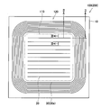
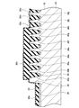
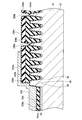
- the semiconductor device 100 of the present embodiment has an element region 110 through which a current flows and a termination region 120 surrounding the element region 110 in a semiconductor substrate 10.
- the semiconductor device 100 of this embodiment is a power MOSFET.
- a plurality of gate trenches 20 are formed in parallel.
- a plurality of termination trenches 30 surrounding the outside of the element region 110 are formed.
- Each termination trench 30 makes a round around the outside of the element region 110.
- illustration of various insulating layers, electrodes, wirings, and the like formed on the upper surface of the semiconductor substrate 10 is omitted for easy understanding.
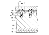
- an n-type drift region 12 is formed in the semiconductor substrate 10 in the element region 110.
- an n + -type source region 11 is formed in a range facing the surface of the semiconductor substrate 10.
- a p-type body region 13 is formed below the source region 11 and above the drift region 12.
- An n + -type drain region 14 is formed in a range facing the back surface of the semiconductor substrate 10.
- the upper surface of the source region 11 is ohmically connected to the source electrode 15.
- the lower surface of the drain region 14 is ohmically connected to the drain electrode 18.
- a plurality of gate trenches 20 are formed on the surface of the semiconductor substrate 10 in the element region 110.
- a p-type floating region 26 is formed at the lower end of the gate trench 20.
- a buried insulating layer 32 a is formed in the lower part inside the gate trench 20.
- a gate insulating film 22 is formed above the buried insulating layer 32 a and on the inner side surface of the gate trench 20.
- a gate electrode 24 that fills the gate trench 20 is formed inside the gate insulating film 22.
- An interlayer insulating film 40 is formed on the upper surface of the gate electrode 24.
- the gate electrode 24 is electrically insulated from the source electrode 15 by the interlayer insulating film 40.
- the contents of phosphorus and boron per unit volume in the interlayer insulating film 40 are larger than the contents of phosphorus and boron per unit volume in the buried insulating layer 32.
- an n-type drift region 12 and an n + -type drain region 14 are also formed in the semiconductor substrate 10 in the termination region 120.
- the drift region 12 and the drain region 14 in the termination region 120 are continuous with the drift region 12 and the drain region 14 in the element region 110. Even in the termination region 120, the lower surface of the drain region 14 is in ohmic contact with the drain electrode 18.
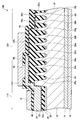
- a plurality of termination trenches 30 a to 30 j are formed on the surface of the semiconductor substrate 10 in the termination region 120. Each of the termination trenches 30a to 30j is formed at substantially the same depth as the gate trench 20 in the element region 110. A p-type floating region 36 is formed at the lower end of each termination trench 30a-30j. In the present specification, the plurality of termination trenches 30a to 30j shown in FIG. 2 may be collectively referred to as “termination trench 30”.
- a buried insulating layer 32b is formed inside the termination trenches 30a to 30g close to the element region 110.
- the buried insulating layer 32 b is also stacked on the upper surface of the semiconductor substrate 10 in the termination region 120.
- the buried insulating layer 32b in the termination region 120 is an insulating layer having characteristics similar to those of the buried insulating layer 32a in the element region 110.
- buried insulating layers 32c and 32d are provided inside the termination trenches 30h, 30i, and 30j provided at positions farther from the element region 110 than the termination trenches 30a to 30g, respectively. , 32e are formed.
- the buried insulating layers 32 c, 32 d, and 32 e are not formed on the upper surface of the semiconductor substrate 10.
- the upper surfaces of the buried insulating layers 32c, 32d, and 32e are located in the termination trenches 30h, 30i, and 30j. That is, the buried insulating layers 32c, 32d, and 32e are not continuous with each other.
- the buried insulating layer 32c is not continuous with the buried insulating layer 32b.
- the buried insulating layers 32c, 32d, and 32e are also insulating layers having the same characteristics as the buried insulating layer 32a in the element region 110.
- a gate insulating film 22 is formed on the upper surfaces of the buried insulating layers 32b, 32c, 32d, and 32e.
- the gate insulating film 22 in the termination region 120 is continuous with the gate insulating film 22 in the element region 110.
- the gate insulating film 22 is also formed on the upper surface of the partition wall between the termination trenches 30g and 30h, the upper surface of the partition wall between the termination trenches 30h and 30i, and the upper surface of the partition wall between the termination trenches 30i and 30j.
- a part of the gate electrode 24 formed in the element region 110 is extended on the upper surface of the portion of the gate insulating film 22 in the termination region 120 formed on the upper surface of the buried insulating layer 32b.
- An interlayer insulating film 40 is formed on the upper surface of the gate electrode 24 and on the upper surface of the gate insulating film 22 in a range where the gate electrode 24 is not formed.
- the interlayer insulating film 40 in the termination region 120 is continuous with the interlayer insulating film 40 in the element region 110.
- a contact hole 42 is formed in a portion of the interlayer insulating film 40 in the termination region 120 formed on the upper surface of the gate electrode 24.
- a gate wiring 44 is formed on the upper surface of the interlayer insulating film 40 in the termination region 120. The gate wiring 44 passes through the contact hole 42 and is electrically connected to the gate electrode 24.
- the gate wiring 44 is formed above the buried insulating layer 32b and is not formed above the buried insulating layers 32c, 32d, and 32e.
- the gate wiring 44 has a portion where the buried insulating layer 32b and the interlayer insulating film 40 are formed on the upper surface of the semiconductor substrate 10 (that is, a thick insulating layer is formed). Formed on the upper surface of the semiconductor substrate 10 and formed on the upper surface of the semiconductor substrate 10 (that is, the portion where the thin insulating layer is formed, above the termination trenches 30h to 30j). It has not been.
- a semiconductor substrate 10 in which a plurality of gate trenches 20 and a plurality of termination trenches 30a to 30j are formed is prepared.
- the semiconductor substrate 10 is made of SiC.
- FIG. 4 only one gate trench 20 is shown.
- a floating region 26 is formed at the lower end of each gate trench 20.
- a floating region 36 is formed at the lower end of each termination trench 30a-30j.
- the drift region 12, the body region 13, and the source region 11 are formed in the semiconductor substrate 10.
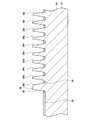
- each gate trench 20, each termination trench 30a to 30j, and the upper surface of the semiconductor substrate 10 that is, the upper surface of the partition wall 28 between the gate trench 20 and the termination trench 30a, and A buried insulating layer 32 is deposited on the upper surface of the partition between the termination trenches 30.
- the buried insulating layer 32 fills each trench and is also laminated on the upper surface of the semiconductor substrate 10.
- the buried insulating layer 32 is formed by performing CVD (Chemical Vapor Deposition) using TEOS (Tetra Ethyl Ortho Silicate) as a raw material.
- a part of the buried insulating layer 32 in the gate trench 20 is removed by etch back.
- part of the buried insulating layer 32 on the upper surface of the partition wall between the gate trench 20 and the termination trench 30a is also removed.
- the buried insulating layer 32 above the termination trenches 30h, 30i, 30j is also removed.
- the etch back is performed by dry etching after forming a protective film above the termination trenches 30a to 30g.
- a buried insulating layer 32b is formed inside the termination trenches 30a to 30g and above the termination trenches 30a to 30g. Further, buried insulating layers 32c, 32d, and 32e are formed inside the termination trenches 30h, 30i, and 30j, respectively.
- the buried insulating layers 32c, 32d, and 32e are not formed on the upper surface of the semiconductor substrate 10, and the upper surfaces of the buried insulating layers 32c, 32d, and 32e are located in the termination trenches 30h, 30i, and 30j. . That is, the buried insulating layers 32c, 32d, and 32e are not continuous with each other. Further, the buried insulating layer 32c is not continuous with the buried insulating layer 32b.
- the buried insulating layers 32a to 32e formed by CVD become dense and stabilized.
- each buried insulating layer shrinks.
- the buried insulating layers 32b to 32e inside and above the plurality of termination trenches 30a to 30j are not continuous with each other. Therefore, the total amount of the insulating material for each of the buried insulating layers 32b to 32e is small, and the amount of shrinkage during the heat treatment can be kept small. As a result, the occurrence of high stress in each buried insulating layer is suppressed.
- the thermal oxidation process also serves as a sacrificial oxide film formation process on the inner wall surface of the gate trench 20. Therefore, a sacrificial oxide film is formed on the inner wall surface of the gate trench 20 by this thermal oxidation treatment. Thereafter, the oxide film formed on the inner wall surface of the gate trench 20 is removed by wet etching. Thereby, the damage layer by dry etching is removed.
- a gate insulating film 22 is formed by CVD or the like.
- a gate electrode 24 is formed in the trench gate 20 by depositing polysilicon in a space in the trench gate 20 secured by etch back. At this time, a part of the gate electrode 24 extends to the upper surface of the gate insulating film 22 formed above the termination trenches 30a to 30d.
- an interlayer insulating film 40 is formed on the upper surface of the semiconductor substrate 10 (see FIG. 2).
- the interlayer insulating film 40 is formed by depositing BPSG (Boron Phosphorus Silicon Glass) by CVD.
- BPSG Bipolar Phosphorus Silicon Glass
- the contents of phosphorus and boron per unit volume in the interlayer insulating film 40 formed by BPSG are more than the contents of phosphorus and boron per unit volume in the buried insulating layers 32a to 32e that are TEOS films. Many.
- the interlayer insulating film 40 is formed on the upper surface of the gate electrode 24 and the upper surface of the gate insulating film 22 in a range where the gate electrode 24 is not formed.
- a contact hole 42 is formed in a portion of the interlayer insulating film 40 formed on the upper surface of the gate electrode 24 (see FIG. 2).
- a metal gate wiring 44 is formed on the upper surface of the interlayer insulating film 40.
- the gate wiring 44 passes through the contact hole 42 and is electrically connected to the gate electrode 24.
- a gate wiring 44 is formed above the buried insulating layer 32b.
- the gate wiring 44 is not formed above the buried insulating layers 32c, 32d, and 32e.
- the regions that have been etched back are located above the buried insulating layer 32b in the region that has not been etched back (that is, the region where the termination trenches 30a to 30g are formed).
- the gate wiring 44 is formed in a non-contact manner with respect to the region in which is formed.
- the drain region 14 is formed on the back surface of the semiconductor substrate 10.
- the drain region 14 is formed by performing laser annealing after implanting impurities into the back surface of the semiconductor substrate 10.
- the drain electrode 18 is formed on the entire back surface of the semiconductor substrate 10.
- the drain electrode 18 can be formed by sputtering, for example.
- the semiconductor device 100 of FIG. 2 is completed by performing the above steps.
- the buried insulating layers 32b to 32e inside and above the plurality of termination trenches 30a to 30j are not continuous with each other. Since the total amount of the insulating material of each of the buried insulating layers 32b to 32e is small, the amount of shrinkage during the heat treatment can be kept small. As a result, the occurrence of high stress in each buried insulating layer is suppressed. As a result, it is possible to suppress the deterioration of the buried insulating layers 32b to 32e, specifically, for example, the generation of cracks.
- the gate wiring 44 is formed above the buried insulating layer 32b and above the buried insulating layers 32c, 32d, and 32e. Absent. That is, in the semiconductor device 100 of this embodiment, the gate wiring 44 is a portion where the buried insulating layer 32b and the interlayer insulating film 40 are formed on the upper surface of the semiconductor substrate 10 (that is, a portion where a thick insulating layer is formed). ) And is formed in a portion where only the interlayer insulating film 40 is formed on the upper surface of the semiconductor substrate 10 (that is, a portion where a thin insulating layer is formed above the termination trenches 30h to 30j). Not. Since the gate wiring is disposed in the portion where the thick insulating layer is formed, a sufficient breakdown voltage of the semiconductor device 100 can be ensured.
- the buried insulating layer 32 above the termination trenches 30h, 30i, and 30j is removed by etch back. After that, regions (that is, termination trenches 30h, 30i, and 30j) that have been etched back are located above the buried insulating layer 32b in the region that has not been etched back (that is, the region where the termination trenches 30a to 30g are formed).
- the gate wiring 44 is formed so as to be non-contact with the formed region). Therefore, the semiconductor device 100 having the above characteristics can be appropriately formed.
- the portion of the buried insulating layer 32b disposed inside the termination trenches 30a to 30g and the buried insulating layers 32c, 32d, and 32e are examples of the “insulating layer in trench”.
- the portion of the buried insulating layer 32b disposed on the upper surface of the semiconductor substrate 10 and the interlayer insulating film 40 are examples of the “upper surface insulating layer”.
- the buried insulating layer 32b and the interlayer insulating film 40 formed above the termination trenches 30e to 30g are examples of the “first portion”.
- the interlayer insulating film 40 formed above the termination trenches 30h to 30j is an example of the “second portion”.
- a portion of the buried insulating layer 32b disposed on the upper surface of the semiconductor substrate 10 is an example of the “first layer”.
- the interlayer insulating film 40 is an example of a “second layer”.
- the region where the termination trenches 30e to 30g are formed is an example of the “first region”.
- the region where the termination trenches 30h to 30j are formed is an example of the “second region”.
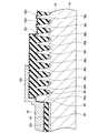
- the semiconductor device 200 of the present embodiment also has an element region 110 and a termination region 120 surrounding the element region 110 in the semiconductor substrate 10, similarly to the semiconductor device 100.
- the semiconductor device 200 of this embodiment is also a power MOSFET.
- a plurality of gate trenches 20 are formed on the surface of the semiconductor substrate 10 in the element region 110.
- a p-type floating region 26 is formed at the lower end of the gate trench 20.
- a first insulating layer 232a is formed inside the vicinity of the lower end of the gate trench 20.
- a second insulating layer 234a is formed above the first insulating layer 232a.
- the refractive index of the first insulating layer 232a is larger than the refractive index of the second insulating layer 234a.
- a gate insulating film 222 is formed above the second insulating layer 234 a and on the inner side surface of the gate trench 20.
- a gate electrode 224 filling the gate trench 20 is formed inside the gate insulating film 222.
- An interlayer insulating film 240 is formed on the upper surface of the gate electrode 224.
- the gate electrode 224 is electrically insulated from the source electrode 15 by the interlayer insulating film 240.
- the contents of phosphorus and boron per unit volume in the interlayer insulating film 240 are larger than the contents of phosphorus and boron per unit volume in the first and second insulating layers 232a and 234a.
- a plurality of termination trenches 30a to 30j are formed on the surface of the semiconductor substrate 10 in the termination region 120.
- Each of the termination trenches 30a to 30j is formed at substantially the same depth as the gate trench 20 in the element region 110.
- a p-type floating region 36 is formed at the lower end of each termination trench 30a-30j.
- a first insulating layer 232b is formed inside the termination trenches 30a to 30j.
- the first insulating layer 232b is also formed on the upper surface portion of the partition between the termination trenches 30a to 30j.
- a second insulating layer 234b is formed inside the first insulating layer 232b in the termination trenches 30a to 30e.
- the second insulating layer 234b is filled in the termination trenches 30a to 30e.
- the second insulating layer 234b is also laminated on the upper surface of the semiconductor substrate 10 in the range where the termination trenches 30a to 30e are formed (that is, the upper surface of the partition wall between the termination trenches).
- the first insulating layer 232b and the second insulating layer 234b are insulating layers having characteristics similar to those of the first insulating layer 232a and the second insulating layer 234a in the element region 110, respectively.
- the refractive index of the first insulating layer 232b is larger than the refractive index of the second insulating layer 234b.
- a third insulating layer 236b is formed on the upper surface of the second insulating layer 234b.
- the refractive index of the third insulating layer 236b is larger than the refractive index of the second insulating layer 234a. Note that the refractive index of the third insulating layer 236b and the refractive index of the first insulating layer 232b may be either larger or equal.
- a second insulating layer 234c is formed inside the first insulating layer 232b in the termination trenches 30f to 30i.
- the second insulating layer 234c is filled in the termination trenches 30f to 30i.
- the second insulating layer 234c is also laminated on the upper surface of the semiconductor substrate 10 in the range where the termination trenches 30f to 30i are formed.
- a third insulating layer 236c is formed on the upper surface of the second insulating layer 234c.
- the second insulating layer 234c and the third insulating layer 236c have characteristics similar to those of the second insulating layer 234b and the third insulating layer 236b.
- a second insulating layer 234d is formed inside the first insulating layer 232b in the termination trench 30j.
- the second insulating layer 234d is filled in the termination trench 30j.
- the second insulating layer 234d is also laminated on the upper surface of the semiconductor substrate 10 in the range where the termination trench 30j is formed.
- a third insulating layer 236d is formed on the upper surface of the second insulating layer 234d.
- the second insulating layer 234d and the third insulating layer 236d also have characteristics similar to those of the second insulating layer 234b and the third insulating layer 236b.
- the second insulating layer 234b and the third insulating layer 236b, and the second insulating layer 234c and the third insulating layer 236c are partitioned by the recess 250a.
- the recess 250 a is filled with part of the gate insulating film 222 and part of the interlayer insulating film 240.
- the recess 250a is formed above the partition between the termination trenches 30e and 30f.
- a first insulating layer 232b exists between the lower end of the recess 250a and the upper surface of the partition wall between the termination trenches 30e and 30f.
- the first insulating layer 232b and the interlayer insulating film 240 are stacked above the partition corresponding to the recess 250a (that is, the partition between the termination trenches 30e and 30f), and the second insulating layer and the third insulating layer 240 are stacked.
- the insulating layer is not laminated.
- a first insulating layer 232b, a second insulating layer 234b, and a third insulating layer 236b are stacked above a partition that does not correspond to the recess 250a (for example, a partition between the termination trenches 30a and 30b). Yes.
- the second insulating layer 234c and the third insulating layer 236c, and the second insulating layer 234d and the third insulating layer 236d are partitioned by the recess 250b.
- the recess 250 b is also filled with a part of the gate insulating film 222 and a part of the interlayer insulating film 240.
- the recess 250b is formed above the partition between the termination trenches 30i and 30j.
- a first insulating layer 232b exists between the lower end of the recess 250b and the upper surface of the partition wall between the termination trenches 30i and 30j.
- the first insulating layer 232b and the interlayer insulating film 240 are stacked above the partition corresponding to the recess 250b (that is, the partition between the termination trenches 30i and 30j), and the second insulating layer and the third insulating layer 240 are stacked.
- the insulating layer is not laminated.
- a first insulating layer 232b, a second insulating layer 234c, and a third insulating layer 236c are stacked above a partition that does not correspond to the recess 250b (for example, a partition between the termination trenches 30f and 30g). Yes.
- the insulating layer (specifically, the second insulating layer and the third insulating layer) formed on the upper surface of the semiconductor substrate 10 in the termination region 120 is a recess. It is divided into three parts by 250a and 250b. Further, the interval between two adjacent recesses 250a and 250b is longer than the interval between two adjacent termination trenches (for example, termination trenches 30a and 30b).
- a gate insulating film 222 is formed on the upper surfaces of the third insulating layers 236b, 236c, and 236d and the inner surfaces of the recesses 250a and 250b in the termination region 120.
- the gate insulating film 222 in the termination region 120 is continuous with the gate insulating film 222 in the element region 110.
- a part of the gate electrode 224 formed in the element region 110 is extended to a part of the upper surface of the gate insulating film 222 in the termination region 120 (specifically, above the third insulating layer 236b). Yes.
- An interlayer insulating film 240 is formed on the upper surface of the gate electrode 224 and the upper surface of the gate insulating film 222 in a range where the gate electrode 224 is not formed.
- the interlayer insulating film 240 in the termination region 120 is continuous with the interlayer insulating film 240 in the element region 110. As described above, part of the interlayer insulating film 240 is filled in the recesses 250a and 250b.
- a contact hole 242 is formed in a portion of the interlayer insulating film 240 in the termination region 120 formed on the upper surface of the gate electrode 224.
- a gate wiring 244 is formed on the upper surface of the interlayer insulating film 240 in the termination region 120. The gate wiring 244 passes through the contact hole 242 and is electrically connected to the gate electrode 224.
- the semiconductor substrate 10 in which a plurality of gate trenches 20 and a plurality of termination trenches 30 are formed is prepared (see FIG. 4).
- the inner surface of each gate trench 20, the inner surfaces of the termination trenches 30a to 30j, and the upper surface of the semiconductor substrate 10 that is, the upper surface of the partition wall 28 between the gate trench 20 and the termination trench 30a
- the 1st insulating layer 232 is deposited on the upper surface of the partition between each termination
- the first insulating layer 232 is formed to a thickness that covers the inner surface of each gate trench 20, the inner surface of each termination trench 30, and the upper surface of the semiconductor substrate 10.
- the first insulating layer 232 is not formed to a thickness that fills each trench.
- the first insulating layer 232 is formed by performing CVD using TEOS as a raw material.
- the first insulating layer 232 When the first insulating layer 232 is formed, CVD is performed under a low pressure. By performing CVD under a low pressure, the deposition rate (that is, the deposition rate) is decreased, and the first insulating layer 232 that is a dense insulating layer can be formed. Note that when CVD is performed under a low pressure, the embedding property of the first insulating layer 232 is not very good. However, since the first insulating layer 232 is formed thin enough to cover each surface, the embedding property is not a problem.
- the first insulating layer 232 can be preferably grown.
- a second insulating layer 234 is deposited on the upper surface of the formed first insulating layer 232.
- the second insulating layer 234 fills the gate trenches 20 and the termination trenches 30a to 30j and is also laminated on the upper surface of the semiconductor substrate 10.
- the second insulating layer 234 is formed by performing CVD using TEOS as a raw material. However, when the second insulating layer 234 is formed, CVD is performed under a pressure higher than that in the case of forming the first insulating layer 232.
- the deposition rate can be increased and the second insulating layer 234 which is a sparse insulating layer can be formed.
- the second insulating layer 234, which is a sparse insulating layer, is excellent in embedding properties in the trench, so that formation of voids in the trench can be suppressed. Therefore, the second insulating layer 234 can be preferably formed without forming a void in the trench.
- a third insulating layer 236 is deposited on the upper surface of the formed second insulating layer 234.
- the third insulating layer 236 is formed by performing CVD using TEOS as a raw material, similarly to the first insulating layer 232 and the second insulating layer 234.
- CVD is performed under a lower pressure than when the second insulating layer 234 is formed. Accordingly, the third insulating layer 236 that is a dense insulating layer can be formed on the upper surface of the second insulating layer 234.
- CVD under a low pressure the embedding property of the insulating material is poor, but since the third insulating layer 236 is formed on a flat surface, the embedding property is not a problem.
- the third insulating layer 236 above the gate trench 20 is removed by etch back.
- part of the first and second insulating layers 232 and 234 in the gate trench 20 is also removed.
- a part of the insulating layers 232, 234 and 236 on the upper surface of the partition wall 28 between the gate trench 20 and the termination trench 30a is also removed.
- Etch back is performed by forming a protective film above the termination trenches 30a to 30j and then performing dry etching. As a result, a part of the first insulating layer 232a and a part of the second insulating layer 234a remain in the gate trench 20.
- the first insulating layer 232b, the second insulating layer 234x, and the third insulating layer 236x remain inside and above the termination trenches 30a to 30j.
- the upper surface shape of the second insulating layer 234a remaining in the gate trench 20 becomes flat.
- the second insulating layer 234a in the gate trench 20 can exhibit suitable insulating performance.
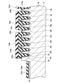
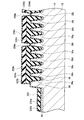
- the second insulating layer 234x and a part of the third insulating layer 236x are dry-etched to form the recesses 250a and 250b.
- the dry etching is performed by forming a protective film having an opening at a position where the recesses 250a and 250b are formed above the semiconductor substrate 10.
- the recesses 250a and 250b are formed so that the lower end penetrates the second insulating layer 234x and the third insulating layer 236x and reaches the first insulating layer 232b.
- the recess 250a, the second insulating layer 234b and the third insulating layer 236b, and the second insulating layer 234c and the third insulating layer 236c are separated from each other.
- the recess 250b the second insulating layer 234c and the third insulating layer 236c, and the second insulating layer 234d and the third insulating layer 236d are separated from each other.
- the first insulating layers 232a and 232b, the second insulating layers 234a to 234d, and the third insulating layers 236b to 236d formed by CVD are densified and stabilized.
- Each insulating layer shrinks during the heat treatment.
- the first insulating layers 232a and 232b and the third insulating layers 236b to 236d which are dense insulating layers are less likely to shrink than the second insulating layers 234a to 234d which are sparse insulating layers.
- the insulating layer (specifically, the second insulating layer and the third insulating layer) formed on the upper surface of the semiconductor substrate 10 is divided into three portions by the recesses 250a and 250b. Since the total amount of the insulating layer per divided portion is reduced, the influence of shrinkage is reduced. Therefore, it is suppressed that a high stress arises in an insulating layer. As a result, deterioration of the first insulating layers 232a and 232b, the second insulating layers 234a to 234d, and the third insulating layers 236b to 236d, specifically, for example, occurrence of cracks can be suppressed.
- the refractive indexes of the first insulating layers 232a and 232b and the third insulating layers 236b to 236d are larger than those of the second insulating layers 234a to 234d.
- the thermal oxidation process also serves as a sacrificial oxide film formation process on the inner wall surface of the gate trench 20. Therefore, a sacrificial oxide film is formed on the inner wall surface of the gate trench 20 by this thermal oxidation treatment. Thereafter, the oxide film formed on the inner wall surface of the gate trench 20 is removed by wet etching. Thereby, the damage layer by dry etching is removed.
- a gate insulating film 222 is formed by CVD or the like.
- a gate electrode 224 is formed in the trench gate 20 by depositing polysilicon in a space secured by etch back. At this time, part of the gate electrode 224 extends to the upper surface of the gate insulating film 222 formed above the third insulating layer 236b.
- an interlayer insulating film 240 is formed on the upper surface of the semiconductor substrate 10 (see FIG. 9).
- the interlayer insulating film 240 is formed by depositing BPSG by CVD.
- the contents of phosphorus and boron per unit volume in the interlayer insulating film 240 formed by BPSG are the same as the amounts of phosphorus and boron per unit volume in the first and second insulating layers 232a and 234a that are TEOS films. More than content.
- the interlayer insulating film 240 is formed on the upper surface of the gate electrode 224 and the upper surface of the gate insulating film 222 in a range where the gate electrode 224 is not formed.
- a contact hole 242 is formed in a portion of the interlayer insulating film 240 formed on the upper surface of the gate electrode 224 (see FIG. 9).
- a metal gate wiring 244 is formed on the upper surface of the interlayer insulating film 240. The gate wiring 244 passes through the contact hole 242 and is electrically connected to the gate electrode 224.
- the drain region 14 is formed on the back surface of the semiconductor substrate 10.
- the drain region 14 is formed by performing laser annealing after implanting impurities into the back surface of the semiconductor substrate 10.
- the drain electrode 18 is formed on the entire back surface of the semiconductor substrate 10.
- the drain electrode 18 can be formed by sputtering, for example.
- the semiconductor device 200 of FIG. 9 is completed by performing the above steps.
- the insulating layer (specifically, the second insulating layer and the third insulating layer) formed on the upper surface of the semiconductor substrate 10 in the termination region 120 includes the recess 250a, It is divided into three parts by 250b. Since the total amount of the insulating layer per divided part is reduced, the influence of shrinkage of the insulating material in the manufacturing process is reduced. Therefore, excessive stress is suppressed from being generated in the insulating material during the manufacturing process of the semiconductor device. As a result, the occurrence of cracks in the first insulating layers 232a and 232b, the second insulating layers 234a to 234d, and the third insulating layers 236b to 236d can be suppressed.
- the refractive indexes of the first insulating layers 232a and 232b and the third insulating layers 236b to 236d are larger than the refractive indexes of the second insulating layers 234a to 234d.
- the first insulating layers 232a and 232b and the third insulating layers 236b to 236d are unlikely to shrink during the manufacturing process of the semiconductor device 200.
- the second insulating layers 234 a to 234 d tend to shrink during the manufacturing process of the semiconductor device 200.
- the shrinkage of the insulating material in the manufacturing process of the semiconductor device 200 is performed. It is possible to prevent an excessive stress caused by. Therefore, in the manufacturing process of the semiconductor device 200, cracks are unlikely to occur in the insulating layer in the trench.
- the first insulating layers 232a and 232b are not so well embedded in the manufacturing process of the semiconductor device 200, but the first insulating layers 232a and 232b are formed so as to cover the inner surface of the trench.
- the embedding property of the insulating material is not a problem.
- the second insulating layers 234a to 234b are formed on the surfaces of the first insulating layers 232a and 232b, the second insulating layers 234a to 234b are preferably formed because the embedding property of the insulating material is good. be able to. Therefore, in the manufacturing process of the semiconductor device 200, voids are unlikely to occur in the insulating layer in the trench. That is, in the semiconductor device 200, voids and cracks due to voids are unlikely to occur in the insulating layer during the manufacturing process.
- the semiconductor device 200 of the present embodiment includes third insulating layers 236b to 236d on the upper surfaces of the second insulating layers 234b to 234d. Since a thick insulating layer can be formed below the gate wiring 44, the semiconductor device 200 can have a high breakdown voltage.
- the first insulating layer 232 that is a dense insulating layer, the second insulating layer 234 that is a sparse insulating layer, and the third insulating layer 236 that is a dense insulating layer. are deposited in this order (see FIGS. 11 to 13), and recesses 250a and 250b are formed (see FIG. 15). Since the semiconductor device 200 is manufactured by such a process, according to the manufacturing method of the present embodiment, the semiconductor device 200 having the above advantages can be suitably formed.
- the first insulating layers 232a and 232b, the second insulating layers 234a to 234d, and the third insulating layers 236b to 236d are examples of the “first layer”.
- the interlayer insulating film 240 is an example of a “second layer”.
- the third insulating layers 236b to 236d are formed on the upper surfaces of the second insulating layers 234b to 234d.
- the third insulating layers 236b to 236d may be omitted in the semiconductor device 200 of the second embodiment.
- the gate insulating film 222 may be formed on the upper surfaces of the second insulating layers 234b to 234d.
- Mode 2 In the first embodiment, as shown in FIG. 2, no buried insulating layer is formed on the upper surface of the semiconductor substrate 10 in the range where the termination trenches 30h, 30i, 30j are formed. .
- the present invention is not limited to this, and a part of the buried insulating layer may also be formed on the upper surface of the semiconductor substrate 10 in a range where the termination trenches 30h, 30i, and 30j are formed.
- the buried insulating layer above the termination trenches 30h, 30i, and 30j is preferably thinner than the buried insulating layer above the termination trenches 30a to 30g.
- the second insulating layer 234 or the third insulating layer 236 may be thinly disposed below the recesses 250a and 250.
- the semiconductor substrate 10 is formed of SiC.
- the semiconductor substrate 10 may be made of Si.
- the semiconductor devices 100 and 200 are power MOSFETs.
- the semiconductor devices 100 and 200 may be arbitrary semiconductor devices as long as they are trench gate type semiconductor devices. it can.
- the semiconductor devices 100 and 200 may be IGBTs.
Landscapes
- Internal Circuitry In Semiconductor Integrated Circuit Devices (AREA)
- Formation Of Insulating Films (AREA)
- Electrodes Of Semiconductors (AREA)
- Chemical & Material Sciences (AREA)
- Composite Materials (AREA)
Abstract
終端領域の絶縁層が劣化することを抑制することができる技術を開示する。半導体装置100は、素子領域110と、素子領域110を取り囲む終端領域120が形成されている半導体基板10を有する。素子領域110は、ゲートトレンチ20と、ゲートトレンチ20の内面を覆うゲート絶縁膜22と、ゲート絶縁膜22の内側に配置されているゲート電極24と、を有している。終端領域120は、素子領域110の周囲に形成されている複数の終端トレンチ30a~30jと、複数の終端トレンチ30a~30jのそれぞれの内側に配置されている埋込絶縁層32b~32eを有している。埋込絶縁層32bは、半導体基板10の上面にも形成されている。半導体基板10の上面には層間絶縁膜40が形成されている。ゲート配線44は、埋込絶縁層32bの上方に形成されており、埋込絶縁層32c~32eの上方には形成されていない。
Description
本出願は、2013年12月25日に出願された日本特許出願特願2013-267786の関連出願であり、この日本特許出願に基づく優先権を主張するものであり、この日本特許出願に記載された全ての内容を、本明細書を構成するものとして援用する。
本明細書で開示する技術は、半導体装置に関する。
日本特許第4735235号公報(以下、特許文献1という)には、素子領域と、素子領域の外側に配置された終端領域とが形成されている半導体基板を有する半導体装置が開示されている。素子領域は、ゲートトレンチと、ゲートトレンチの内面を覆うゲート絶縁膜と、ゲート絶縁膜の内側に設けられているゲート電極とを有している。終端領域は、終端トレンチと、終端トレンチの内部を充填するとともに、半導体基板の上面を覆う終端絶縁層とを有している。終端絶縁層の上面には、ゲート電極と電気的に接続するゲート配線が配置されている。
終端絶縁層は、絶縁材料を堆積させ、その後熱処理を行うことによって形成される。特許文献1の技術のように、終端絶縁層を、終端領域の半導体基板の上面全域に均一に堆積させると、その後の熱処理温度が高い場合に絶縁材料が収縮し、劣化が生じやすくなる。
本明細書では、終端領域の絶縁層が劣化することを抑制することができる半導体装置及びその製造方法を開示する。
本明細書で開示する一つの半導体装置は、素子領域と、素子領域を取り囲む終端領域が形成されている半導体基板を有する半導体装置である。素子領域は、ゲートトレンチと、ゲートトレンチの内面を覆うゲート絶縁膜と、ゲート絶縁膜の内側に配置されているゲート電極と、を有している。終端領域は、素子領域の周囲に形成されている複数の終端トレンチと、複数の終端トレンチのそれぞれの内側に配置されているトレンチ内絶縁層と、終端領域内の半導体基板の上面に配置されている上面絶縁層と、を有している。上面絶縁層は、第1部分と、第1部分よりも厚みが薄く、第1部分よりも素子領域から離れた位置に配置されている第2部分を有している。ゲート配線は、第1部分の上面に配置されており、第2部分の上面に配置されていない。
上記の半導体装置では、上面絶縁層は、第1部分と、第1部分よりも厚みが薄く、第1部分よりも素子領域から離れた位置に配置されている第2部分を有している。ゲート配線は、第1部分の上面に配置されており、第2部分の上面に配置されていない。即ち、ゲート配線が配置されていない第2部分を第1部分よりも薄く形成したことで、均一の厚みを有する上面絶縁層を終端領域の全域に形成する場合に比べて、上面絶縁層に用いる絶縁材料の総量を少なくすることができる。絶縁材料の総量を少なくすることにより、半導体装置を製造過程での絶縁材料の収縮量を小さく抑えることができる。これにより、半導体装置の製造過程で絶縁材料に過大な応力が生じることが防止される。従って、絶縁層が劣化することを抑制することができる。
上面絶縁層は、第1層と、リンとボロンの単位体積当たりの含有量が第1層よりも多く、第1層の上面に配置されている第2層を有していてもよい。第1領域内の上面絶縁層が、第1層と第2層を有していてもよい。第1領域よりも素子領域から離れた位置の第2領域内の上面絶縁層が、第2層と第1領域内の第1層よりも薄い第1層を有している、または、第2層を有しており第1層を有していなくてもよい。ゲート配線は、第1領域内の上面絶縁層の上面に配置されており、第2領域内の上面絶縁層の上面に配置されていなくてもよい。
この構成によると、ゲート配線が配置される第1領域内の第1層を厚く形成することができる。従って、第2領域よりも厚い第1領域を適切に形成することができる。
本明細書で開示する一つの半導体装置の製造方法は、絶縁層を、複数のトレンチを有する半導体基板の各トレンチ内と、半導体基板の上面に形成する工程と、複数のトレンチのうちの一部のトレンチが形成されている領域の半導体基板の上面に形成されている絶縁層をエッチバックする工程と、エッチバックをしなかった絶縁層の上面に、エッチバックした領域に対して非接触となるように、ゲート配線を形成する工程、を有する。
上記の製造方法によると、エッチバックをしなかった領域に厚い絶縁層を形成し、その上面にゲート配線が配置された半導体装置を形成することができる。即ち、ゲート配線が配置されていない領域の絶縁層を薄く形成することで、絶縁層を形成する絶縁材料の総量を少なくすることができる。絶縁材料の総量を少なくすることにより、半導体装置の製造過程における絶縁層の収縮量を小さく抑えることができる。これにより、半導体装置の製造過程で絶縁材料の収縮による過大な応力が生じることが防止されることにより、絶縁層が劣化することを抑制することができる。
本明細書で開示するもう一つの半導体装置は、素子領域と、素子領域を取り囲む終端領域が形成されている半導体基板を有する半導体装置である。素子領域は、ゲートトレンチと、ゲートトレンチの内面を覆うゲート絶縁膜と、ゲート絶縁膜の内側に配置されているゲート電極と、を有している。終端領域は、素子領域の周囲に形成されている複数の終端トレンチと、複数の終端トレンチのそれぞれの内側、及び、半導体基板の上面に形成されている絶縁層を有している。絶縁層は、第1層と、リンとボロンの単位体積当たりの含有量が第1層よりも多く、第1層の上面に配置されている第2層を有している。第1層の上面に、複数の凹部が形成されている。各凹部は、隣り合う終端トレンチの間の隔壁に沿って延設されている。隣り合う凹部の間隔は、隣り合う終端トレンチの間隔よりも長い。各凹部内に、第2層が充填されている。絶縁層の上面に、ゲート配線が配置されている。
上記の半導体装置では、第1層に凹部が形成されている。凹部では第1層の厚みが薄いため、第1層に応力が生じ難い。したがって、第1層が収縮等することによって第1層に応力が生じたとしても、凹部によって応力が緩和されるため、第1層に過大な応力が生じることが防止されることにより、絶縁層が劣化することを抑制することができる。
第1層が、複数の終端トレンチのそれぞれの内面を覆う第1の絶縁層と、第1の絶縁層で覆われた複数の終端トレンチの内側に充填されている第2の絶縁層を有していてもよい。第1の絶縁層の屈折率は、第2の絶縁層の屈折率よりも大きくてもよい。
上記の半導体装置では、第1の絶縁層の屈折率は、第2の絶縁層の屈折率よりも大きい。第1の絶縁層は、半導体装置の製造過程において収縮し難い。第2の絶縁層は、半導体装置の製造過程において収縮し易い。第1の絶縁層と第2の絶縁層が終端トレンチ内に配置されていることで、半導体装置の製造過程において絶縁材料に過大な応力が生じることが防止される。従って、この半導体装置の製造過程では、終端トレンチ内の絶縁層が劣化することを抑制することができる。また、第1の絶縁層は半導体装置の製造過程において埋め込み性があまり良くないが、第1の絶縁層は終端トレンチの内面を覆うように形成されるため、第1の絶縁層の形成時には絶縁材料の埋め込み性は問題とならない。その後、第1の絶縁層の表面に第2の絶縁層を形成する際には、絶縁材料の埋め込み性が良いので、好適に第2の絶縁層を形成することができる。従って、この半導体装置の製造過程では、終端トレンチ内の絶縁層にボイドが発生し難い。
凹部に対応する隔壁上に、第1の絶縁層と第2層が積層されており、第2の絶縁層が積層されていなくてもよい。凹部に対応しない隔壁上に、第1の絶縁層と、第2の絶縁層と、第2層が積層されていてもよい。
この構成によると、半導体装置の製造過程で収縮し易い第2の絶縁層が凹部において不連続となるため、第2の絶縁層に生じる応力を緩和することができる。これによって、絶縁層の劣化をより適切に抑制することができる。
第1層は、第2の絶縁層の上面に形成されている第3の絶縁層を有していてもよい。第3の絶縁層の屈折率は、第2の絶縁層の屈折率よりも大きくてもよい。
屈折率が大きい第3の絶縁層は、半導体装置の製造過程において収縮し難い。この構成によると、半導体基板の上面の第1層(即ち、第1の絶縁層、第2の絶縁層、及び、第3の絶縁層)が劣化することを抑制することができる。また、半導体基板の上面に厚い第1層を形成することができるため、半導体装置を高耐圧化することもできる。
(第1実施例)
(半導体装置100の構造)
図1に示すように、本実施例の半導体装置100は、半導体基板10中に、電流が流れる素子領域110と、その素子領域110を取り囲む終端領域120とを有している。本実施例の半導体装置100は、パワーMOSFETである。
(半導体装置100の構造)
図1に示すように、本実施例の半導体装置100は、半導体基板10中に、電流が流れる素子領域110と、その素子領域110を取り囲む終端領域120とを有している。本実施例の半導体装置100は、パワーMOSFETである。
図1に示すように、素子領域110には、複数本のゲートトレンチ20が平行に形成されている。終端領域120には、素子領域110の外側を囲む複数本の終端トレンチ30が形成されている。各終端トレンチ30は、素子領域110の外側を一巡している。なお、図1では、理解の容易のために、半導体基板10の上面に形成されている各種絶縁層、電極、配線等の図示を省略している。
図2、図3を参照して、素子領域110内及び終端領域120内の構造を説明する。図2に示すように、素子領域110の半導体基板10の中には、n型のドリフト領域12が形成されている。また、図3に示すように、半導体基板10の表面に臨む範囲には、n+型のソース領域11が形成されている。また、ソース領域11の下方であって、ドリフト領域12の上方には、p型のボディ領域13が形成されている。半導体基板10の裏面に臨む範囲には、n+型のドレイン領域14が形成されている。ソース領域11の上面は、ソース電極15に対してオーミック接続している。ドレイン領域14の下面は、ドレイン電極18に対してオーミック接続している。
また、上記の通り、素子領域110内の半導体基板10の表面には複数のゲートトレンチ20が形成されている。ゲートトレンチ20の下端部には、p型のフローティング領域26が形成されている。ゲートトレンチ20の内側の下部には、埋込絶縁層32aが形成されている。埋込絶縁層32aの上方、及び、ゲートトレンチ20の内側面には、ゲート絶縁膜22が形成されている。ゲート絶縁膜22の内側には、ゲートトレンチ20内に充填されるゲート電極24が形成されている。ゲート電極24の上面には、層間絶縁膜40が形成される。層間絶縁膜40により、ゲート電極24は、ソース電極15から電気的に絶縁されている。層間絶縁膜40における単位体積当たりのリンとボロンの含有量は、埋込絶縁層32における単位体積当たりのリンとボロンの含有量よりも多い。
図2に示すように、終端領域120の半導体基板10の中にも、n型のドリフト領域12、及び、n+型のドレイン領域14が形成されている。終端領域120内のドリフト領域12及びドレイン領域14は、素子領域110内のドリフト領域12及びドレイン領域14と連続している。終端領域120でも、ドレイン領域14の下面は、ドレイン電極18に対してオーミック接続している。
終端領域120内の半導体基板10の表面には複数の終端トレンチ30a~30jが形成されている。各終端トレンチ30a~30jは、素子領域110内のゲートトレンチ20と略同じ深さに形成されている。各終端トレンチ30a~30jの下端部には、p型のフローティング領域36が形成されている。本明細書では、図2に示す複数の終端トレンチ30a~30jのことを「終端トレンチ30」と総称する場合がある。
複数の終端トレンチ30a~30jのうち、素子領域110に近い終端トレンチ30a~30gの内側には、埋込絶縁層32bが形成されている。埋込絶縁層32bは、終端領域120内の半導体基板10の上面にも積層されている。終端領域120内の埋込絶縁層32bは、素子領域110内の埋込絶縁層32aと同様の特性を有する絶縁層である。
複数の終端トレンチ30a~30jのうち、終端トレンチ30a~30gよりも素子領域110から離れた位置に設けられている終端トレンチ30h、30i、30jのそれぞれの内側には、埋込絶縁層32c、32d、32eが形成されている。埋込絶縁層32c、32d、32eは、半導体基板10の上面には形成されていない。埋込絶縁層32c、32d、32eの上面は、終端トレンチ30h、30i、30j内に位置している。即ち、埋込絶縁層32c、32d、32eは、互いに連続していない。また、埋込絶縁層32cは、埋込絶縁層32bとも連続していない。なお、埋込絶縁層32c、32d、32eも、素子領域110内の埋込絶縁層32aと同様の特性を有する絶縁層である。
埋込絶縁層32b、32c、32d、32eの上面には、ゲート絶縁膜22が形成されている。終端領域120のゲート絶縁膜22は、素子領域110のゲート絶縁膜22と連続している。ゲート絶縁膜22は、終端トレンチ30gと30hの間の隔壁の上面、終端トレンチ30hと30iの間の隔壁の上面、及び、終端トレンチ30iと30jの間の隔壁の上面にも形成されている。
終端領域120のゲート絶縁膜22のうち、埋込絶縁層32bの上面に形成されている部分の上面には、素子領域110内に形成されているゲート電極24の一部が延伸されている。そのゲート電極24の上面、及び、ゲート電極24が形成されていない範囲のゲート絶縁膜22の上面には、層間絶縁膜40が形成されている。終端領域120の層間絶縁膜40は、素子領域110の層間絶縁膜40と連続している。終端領域120の層間絶縁膜40のうち、ゲート電極24の上面に形成されている部分には、コンタクトホール42が形成されている。終端領域120の層間絶縁膜40の上面には、ゲート配線44が形成されている。ゲート配線44は、コンタクトホール42を通過して、ゲート電極24と電気的に接続されている。
本実施例の半導体装置100では、ゲート配線44は、埋込絶縁層32bの上方に形成されており、埋込絶縁層32c、32d、32eの上方には形成されていない。言い換えると、本実施例の半導体装置100では、ゲート配線44は、半導体基板10の上面に埋込絶縁層32bと層間絶縁膜40が形成されている部分(即ち、厚い絶縁層が形成されている部分)の上面に形成されており、半導体基板10の上面に層間絶縁膜40しか形成されていない部分(即ち、薄い絶縁層が形成されている部分。終端トレンチ30h~30jの上方)には形成されていない。
(製造方法)
次いで、本実施例の半導体装置100の製造方法を説明する。まず、図4に示すように、複数のゲートトレンチ20と、複数の終端トレンチ30a~30jとが形成された半導体基板10を準備する。本実施例では、半導体基板10はSiCによって形成されている。なお、図4では、ゲートトレンチ20は1本のみを図示している。図4の時点で、各ゲートトレンチ20の下端部には、フローティング領域26が形成されている。また、各終端トレンチ30a~30jの下端部には、フローティング領域36が形成されている。また、この時点で、半導体基板10には、ドリフト領域12、ボディ領域13、及び、ソース領域11が形成されている。
次いで、本実施例の半導体装置100の製造方法を説明する。まず、図4に示すように、複数のゲートトレンチ20と、複数の終端トレンチ30a~30jとが形成された半導体基板10を準備する。本実施例では、半導体基板10はSiCによって形成されている。なお、図4では、ゲートトレンチ20は1本のみを図示している。図4の時点で、各ゲートトレンチ20の下端部には、フローティング領域26が形成されている。また、各終端トレンチ30a~30jの下端部には、フローティング領域36が形成されている。また、この時点で、半導体基板10には、ドリフト領域12、ボディ領域13、及び、ソース領域11が形成されている。
次いで、図5に示すように、各ゲートトレンチ20の内面、各終端トレンチ30a~30j、及び、半導体基板10の上面(即ち、ゲートトレンチ20と終端トレンチ30aの間の隔壁28の上面、及び、各終端トレンチ30間の隔壁の上面)に、埋込絶縁層32を堆積させる。埋込絶縁層32は、各トレンチを充填するとともに、半導体基板10の上面にも積層される。埋込絶縁層32は、TEOS(Tetra Ethyl Ortho Silicate)を原料とするCVD(Chemical Vapor Deposition)を行うことによって形成される。
次いで、図6に示すように、エッチバックによって、ゲートトレンチ20内の埋込絶縁層32の一部を除去する。それとともに、ゲートトレンチ20と終端トレンチ30aとの間の隔壁の上面の埋込絶縁層32の一部も除去する。さらに、終端トレンチ30h、30i、30jの上方の埋込絶縁層32も除去する。エッチバックは、終端トレンチ30a~30gの上方に保護膜を形成した上でドライエッチングを行うことによって行う。このエッチバックにより、図5で形成された埋込絶縁層32が複数の部分に分断される。即ち、ゲートトレンチ20内では、下部付近に一部の埋込絶縁層32aが残存する。また、終端トレンチ30a~30gの内側、及び、終端トレンチ30a~30gの上方には、埋込絶縁層32bが形成される。また、終端トレンチ30h、30i、30jのそれぞれの内側には、埋込絶縁層32c、32d、32eが形成される。埋込絶縁層32c、32d、32eは、半導体基板10の上面には形成されておらず、埋込絶縁層32c、32d、32eの上面は、終端トレンチ30h、30i、30j内に位置している。即ち、埋込絶縁層32c、32d、32eは、互いに連続していない。また、埋込絶縁層32cは、埋込絶縁層32bとも連続していない。
次いで、半導体基板10に対して熱酸化処理を行う。これにより、CVDによって形成された埋込絶縁層32a~32eが緻密化し、安定化する。熱処理中に、各埋込絶縁層は収縮する。上記の通り、複数の終端トレンチ30a~30jの内側及び上方の埋込絶縁層32b~32eは、互いに連続していない。そのため、各埋込絶縁層32b~32eの絶縁材料の総量が少なく、熱処理時の収縮量を小さく抑えることができる。そのため、各埋込絶縁層に高い応力が生じることが抑制される。その結果、埋込絶縁層32b~32eが劣化すること、具体的には例えばクラックが生じることを抑制することができる。また、この熱酸化処理は、ゲートトレンチ20の内壁面への犠牲酸化膜の形成処理も兼ねている。そのため、この熱酸化処理により、ゲートトレンチ20の内壁面には犠牲酸化膜が形成される。その後、ゲートトレンチ20の内壁面に形成された酸化膜をウェットエッチングによって除去する。これにより、ドライエッチングによるダメージ層が除去される。
次いで、図7に示すように、CVD等によってゲート絶縁膜22を形成する。
次いで、図8に示すように、エッチバックによって確保されたトレンチゲート20内のスペースにポリシリコンを堆積させることにより、トレンチゲート20内にゲート電極24を形成する。この際、ゲート電極24の一部は、終端トレンチ30a~30dの上方に形成されたゲート絶縁膜22の上面まで伸びる。
その後、半導体基板10の上面に層間絶縁膜40を形成する(図2参照)。層間絶縁膜40は、BPSG(Boron Phosphorus Silicon Glass)をCVDで堆積させることによって形成される。上記の通り、BPSGにより形成される層間絶縁膜40における単位体積当たりのリンとボロンの含有量は、TEOS膜である埋込絶縁層32a~32eにおける単位体積当たりのリンとボロンの含有量よりも多い。この結果、ゲート電極24の上面、及び、ゲート電極24が形成されていない範囲のゲート絶縁膜22の上面に、層間絶縁膜40が形成される。
その後、層間絶縁膜40のうちゲート電極24の上面に形成されている部分に、コンタクトホール42を形成する(図2参照)。次いで、層間絶縁膜40の上面に金属製のゲート配線44を形成する。ゲート配線44は、コンタクトホール42を通過して、ゲート電極24と電気的に接続される。これにより、埋込絶縁層32bの上方にゲート配線44が形成される。埋込絶縁層32c、32d、32eの上方にはゲート配線44は形成されない。言い換えると、エッチバックをしなかった領域(即ち、終端トレンチ30a~30gが形成されている領域)の埋込絶縁層32bの上方に、エッチバックをした領域(即ち、終端トレンチ30h、30i、30jが形成されている領域)に対して非接触となるように、ゲート配線44が形成される。
さらにその後、半導体基板10の裏面にドレイン領域14を形成する。ドレイン領域14は、半導体基板10の裏面に不純物を注入した後に、レーザーアニールを行うことで形成される。次いで、半導体基板10の裏面全面にドレイン電極18を形成する。ドレイン電極18は、例えば、スパッタリングによって形成することができる。
以上の各工程を行うことにより、図2の半導体装置100が完成する。
本実施例の半導体装置100では、複数の終端トレンチ30a~30jの内側及び上方の埋込絶縁層32b~32eは、互いに連続していない。埋込絶縁層32b~32eのそれぞれの絶縁材料の総量が少ないため、熱処理時の収縮量を小さく抑えることができる。そのため、各埋込絶縁層に高い応力が生じることが抑制される。その結果、埋込絶縁層32b~32eが劣化すること、具体的には例えばクラックが生じることを抑制することができる。
図2に示すように、本実施例の半導体装置100では、ゲート配線44は、埋込絶縁層32bの上方に形成されており、埋込絶縁層32c、32d、32eの上方には形成されていない。即ち、本実施例の半導体装置100では、ゲート配線44は、半導体基板10の上面に埋込絶縁層32bと層間絶縁膜40が形成されている部分(即ち、厚い絶縁層が形成されている部分)の上面に形成されており、半導体基板10の上面に層間絶縁膜40しか形成されていない部分(即ち、薄い絶縁層が形成されている部分。終端トレンチ30h~30jの上方)には形成されていない。厚い絶縁層が形成されている部分にゲート配線を配置しているため、半導体装置100の耐圧を十分確保することができる。
また、本実施例の製造方法では、エッチバックにより、終端トレンチ30h、30i、30jの上方の埋込絶縁層32を除去する。その後、エッチバックをしなかった領域(即ち、終端トレンチ30a~30gが形成されている領域)の埋込絶縁層32bの上方に、エッチバックをした領域(即ち、終端トレンチ30h、30i、30jが形成されている領域)に対して非接触となるように、ゲート配線44を形成する。そのため、上記の特性を備える半導体装置100を適切に形成することができる。
本実施例と請求の範囲の記載の対応関係を説明しておく。埋込絶縁層32bのうち終端トレンチ30a~30gの内側に配置されている部分、及び、埋込絶縁層32c、32d、32eが「トレンチ内絶縁層」の一例である。埋込絶縁層32bのうち半導体基板10の上面に配置されている部分、及び、層間絶縁膜40が「上面絶縁層」の一例である。終端トレンチ30e~30gの上方に形成されている埋込絶縁層32b及び層間絶縁膜40が「第1部分」の一例である。終端トレンチ30h~30jの上方に形成されている層間絶縁膜40が「第2部分」の一例である。埋込絶縁層32bのうち半導体基板10の上面に配置されている部分が「第1層」の一例である。層間絶縁膜40が「第2層」の一例である。終端トレンチ30e~30gが形成されている領域が「第1領域」の一例である。終端トレンチ30h~30jが形成されている領域が「第2領域」の一例である。
(第2実施例)
(半導体装置200の構造)
続いて、図1、図9~図17を参照して、第2実施例の半導体装置200について説明する。図1に示すように、本実施例の半導体装置200も、半導体装置100と同様に、半導体基板10中に素子領域110と、その素子領域110を取り囲む終端領域120とを有している。本実施例の半導体装置200も、パワーMOSFETである。
(半導体装置200の構造)
続いて、図1、図9~図17を参照して、第2実施例の半導体装置200について説明する。図1に示すように、本実施例の半導体装置200も、半導体装置100と同様に、半導体基板10中に素子領域110と、その素子領域110を取り囲む終端領域120とを有している。本実施例の半導体装置200も、パワーMOSFETである。
図9、図10を参照して、素子領域110内及び終端領域120内の構造を説明する。図9、図10では、第1実施例の半導体装置100(図2参照)と共通する要素については同じ符号を用いて示し、詳しい説明を省略する。
図1に示すように、本実施例でも、素子領域110内の半導体基板10の表面には複数のゲートトレンチ20が形成されている。図10に示すように、ゲートトレンチ20の下端部には、p型のフローティング領域26が形成されている。ゲートトレンチ20の下端部付近の内側には、第1の絶縁層232aが形成されている。第1の絶縁層232aの上方には、第2の絶縁層234aが形成されている。第1の絶縁層232aの屈折率は、第2の絶縁層234aの屈折率よりも大きい。第2の絶縁層234aの上方、及び、ゲートトレンチ20の内側面には、ゲート絶縁膜222が形成されている。ゲート絶縁膜222の内側には、ゲートトレンチ20内に充填されるゲート電極224が形成されている。ゲート電極224の上面には、層間絶縁膜240が形成される。層間絶縁膜240により、ゲート電極224は、ソース電極15と電気的に絶縁されている。層間絶縁膜240における単位体積当たりのリンとボロンの含有量は、第1及び第2の絶縁層232a、234aにおける単位体積当たりのリンとボロンの含有量よりも多い。
図9に示すように、終端領域120内の半導体基板10の表面には複数の終端トレンチ30a~30jが形成されている。各終端トレンチ30a~30jは、素子領域110内のゲートトレンチ20と略同じ深さに形成されている。各終端トレンチ30a~30jの下端部には、p型のフローティング領域36が形成されている。
終端トレンチ30a~30jの内側には、第1の絶縁層232bが形成されている。第1の絶縁層232bは、各終端トレンチ30a~30j間の隔壁の上面部分にも形成されている。
終端トレンチ30a~30e内の第1の絶縁層232bの内側には、第2の絶縁層234bが形成されている。第2の絶縁層234bは、終端トレンチ30a~30e内に充填されている。また、第2の絶縁層234bは、終端トレンチ30a~30eが形成されている範囲の半導体基板10の上面(即ち、各終端トレンチ間の隔壁の上面)にも積層されている。第1の絶縁層232b及び第2の絶縁層234bは、それぞれ、素子領域110内の第1の絶縁層232a及び第2の絶縁層234aと同様の特性を有する絶縁層である。即ち、第1の絶縁層232bの屈折率は、第2の絶縁層234bの屈折率よりも大きい。第2の絶縁層234bの上面には、第3の絶縁層236bが形成されている。第3の絶縁層236bの屈折率は、第2の絶縁層234aの屈折率よりも大きい。なお、第3の絶縁層236bの屈折率と、第1の絶縁層232bの屈折率は、どちらが大きくてもよいし、等しくてもよい。
同様に、終端トレンチ30f~30i内の第1の絶縁層232bの内側には、第2の絶縁層234cが形成されている。また、第2の絶縁層234cは、終端トレンチ30f~30i内に充填されている。また、第2の絶縁層234cは、終端トレンチ30f~30iが形成されている範囲の半導体基板10の上面にも積層されている。第2の絶縁層234cの上面には、第3の絶縁層236cが形成されている。第2の絶縁層234c及び第3の絶縁層236cは、第2の絶縁層234b及び第3の絶縁層236bと同様の特性を有する。
同様に、終端トレンチ30j内の第1の絶縁層232bの内側には、第2の絶縁層234dが形成されている。また、第2の絶縁層234dは、終端トレンチ30j内に充填されている。また、第2の絶縁層234dは、終端トレンチ30jが形成されている範囲の半導体基板10の上面にも積層されている。第2の絶縁層234dの上面には、第3の絶縁層236dが形成されている。第2の絶縁層234d及び第3の絶縁層236dも、第2の絶縁層234b及び第3の絶縁層236bと同様の特性を有する。
第2の絶縁層234b及び第3の絶縁層236bと、第2の絶縁層234c及び第3の絶縁層236cとは、凹部250aによって区画されている。凹部250a内には、ゲート絶縁膜222の一部と、層間絶縁膜240の一部が充填されている。凹部250aは、終端トレンチ30e、30fの間の隔壁の上方に形成されている。凹部250aの下端部と、終端トレンチ30e、30fの間の隔壁の上面との間には、第1の絶縁層232bが存在している。即ち、凹部250aに対応する隔壁(即ち、終端トレンチ30e、30fの間の隔壁)の上方には、第1の絶縁層232bと層間絶縁膜240が積層され、第2の絶縁層及び第3の絶縁層は積層されていない。一方、凹部250aに対応しない隔壁(例えば、終端トレンチ30a、30bの間の隔壁)の上方には、第1の絶縁層232b、第2の絶縁層234b、第3の絶縁層236bが積層されている。
同様に、第2の絶縁層234c及び第3の絶縁層236cと、第2の絶縁層234d及び第3の絶縁層236dとは、凹部250bによって区画されている。凹部250b内にも、ゲート絶縁膜222の一部と、層間絶縁膜240の一部が充填されている。凹部250bは、終端トレンチ30i、30jの間の隔壁の上方に形成されている。凹部250bの下端部と、終端トレンチ30i、30jの間の隔壁の上面との間には、第1の絶縁層232bが存在している。即ち、凹部250bに対応する隔壁(即ち、終端トレンチ30i、30jの間の隔壁)の上方には、第1の絶縁層232bと層間絶縁膜240が積層され、第2の絶縁層及び第3の絶縁層は積層されていない。一方、凹部250bに対応しない隔壁(例えば、終端トレンチ30f、30gの間の隔壁)の上方には、第1の絶縁層232b、第2の絶縁層234c、第3の絶縁層236cが積層されている。
即ち、本実施例の半導体装置200では、終端領域120内において、半導体基板10の上面に形成されている絶縁層(具体的には、第2の絶縁層及び第3の絶縁層)は、凹部250a、250bによって、3つの部分に分断されている。また、隣り合う2つの凹部250a、250b同士の間隔は、隣り合う2本の終端トレンチ(例えば終端トレンチ30a、30b)同士の間隔よりも長い。
終端領域120における第3の絶縁層236b、236c、236dの上面、及び、凹部250a、250bの内面には、ゲート絶縁膜222が形成されている。終端領域120のゲート絶縁膜222は、素子領域110のゲート絶縁膜222と連続している。終端領域120のゲート絶縁膜222の上面の一部(具体的には、第3の絶縁層236bの上方)には、素子領域110内に形成されているゲート電極224の一部が延伸されている。
ゲート電極224の上面、及び、ゲート電極224が形成されていない範囲のゲート絶縁膜222の上面には、層間絶縁膜240が形成されている。終端領域120の層間絶縁膜240は、素子領域110の層間絶縁膜240と連続している。上記の通り、層間絶縁膜240の一部は、凹部250a、250b内に充填されている。終端領域120の層間絶縁膜240のうち、ゲート電極224の上面に形成されている部分には、コンタクトホール242が形成されている。終端領域120の層間絶縁膜240の上面には、ゲート配線244が形成されている。ゲート配線244は、コンタクトホール242を通過して、ゲート電極224と電気的に接続されている。
(製造方法)
次いで、本実施例の半導体装置100の製造方法を説明する。まず、複数のゲートトレンチ20と、複数の終端トレンチ30とが形成された半導体基板10を準備する(図4参照)。
次いで、本実施例の半導体装置100の製造方法を説明する。まず、複数のゲートトレンチ20と、複数の終端トレンチ30とが形成された半導体基板10を準備する(図4参照)。
次いで、図11に示すように、各ゲートトレンチ20の内面、各終端トレンチ30a~30jの内面、及び、半導体基板10の上面(即ち、ゲートトレンチ20と終端トレンチ30aの間の隔壁28の上面、及び、各終端トレンチ30間の隔壁の上面)に、第1の絶縁層232を堆積させる。この工程では、第1の絶縁層232は、各ゲートトレンチ20の内面、各終端トレンチ30の内面、及び、半導体基板10の上面を覆う程度の厚さに形成される。第1の絶縁層232は、各トレンチを充填する厚さには形成されない。第1の絶縁層232は、TEOSを原料とするCVDを行うことによって形成される。第1の絶縁層232を形成する際には、低い圧力の下でCVDを実行する。低い圧力の下でCVDを実行することにより、成膜レート(即ち、成膜速度)が遅くなり、密な絶縁層である第1の絶縁層232を形成することができる。なお、低い圧力の下でCVDを実行すると、第1の絶縁層232の埋め込み性があまり良くない。しかしながら、第1の絶縁層232は、各表面を覆う程度に薄く形成されるので、埋め込み性は問題とならない。好適に第1の絶縁層232を成長させることができる。
次いで、図12に示すように、形成された第1の絶縁層232の上面に、第2の絶縁層234を堆積させる。この工程では、第2の絶縁層234は、各ゲートトレンチ20及び各終端トレンチ30a~30jを充填するとともに、半導体基板10の上面にも積層される。第2の絶縁層234は、第1の絶縁層232と同様に、TEOSを原料とするCVDを行うことによって形成される。ただし、第2の絶縁層234を形成する際には、第1の絶縁層232を形成する場合よりも高い圧力の下でCVDを実行する。高い圧力の下でCVDを実行することにより、成膜レートが早くなり、疎な絶縁層である第2の絶縁層234を形成することができる。疎な絶縁層である第2の絶縁層234は、トレンチへの埋め込み性に優れるため、トレンチ内にボイドが形成されることを抑制することができる。従って、トレンチ内にボイドが形成されることなく、好適に第2の絶縁層234を形成することができる。
次いで、図13に示すように、形成された第2の絶縁層234の上面に、第3の絶縁層236を堆積させる。第3の絶縁層236は、第1の絶縁層232及び第2の絶縁層234と同様に、TEOSを原料とするCVDを行うことによって形成される。第3の絶縁層236を形成する際には、第2の絶縁層234を形成する場合よりも低い圧力の下でCVDを実行する。これにより、第2の絶縁層234の上面に、密な絶縁層である第3の絶縁層236を形成することができる。低い圧力の下でのCVDでは絶縁材料の埋め込み性が悪いが、第3の絶縁層236は平坦な表面上に形成されるので、埋め込み性は問題とならない。
次いで、図14に示すように、エッチバックによって、ゲートトレンチ20の上方の第3の絶縁層236を除去する。この際、ゲートトレンチ20内の第1及び第2の絶縁層232、234の一部も併せて除去する。なお、ゲートトレンチ20と終端トレンチ30aとの間の隔壁28の上面の絶縁層232、234、236の一部も併せて除去する。エッチバックは、終端トレンチ30a~30jの上方に保護膜を形成した上でドライエッチングを行うことによって行う。これにより、ゲートトレンチ20内には、一部の第1の絶縁層232a、及び、一部の第2の絶縁層234aが残存する。また、終端トレンチ30a~30jの内側及び上方には、第1の絶縁層232b、第2の絶縁層234x、第3の絶縁層236xが残存する。上述の通り、第2の絶縁層234の形成時にボイドが形成され難いため、ゲートトレンチ20内に残存する第2の絶縁層234aの上面形状は平坦になる。この結果、ゲートトレンチ20内に残存する第2の絶縁層234aに凹部等が形成されないため、ゲートトレンチ20内の第2の絶縁層234aは好適な絶縁性能を発揮することができる。
次いで、図15に示すように、第2の絶縁層234x及び第3の絶縁層236xの一部をドライエッチングし、凹部250a、250bを形成する。ドライエッチングは、凹部250a、250bを形成する位置を開口した保護膜を半導体基板10の上方に形成して行う。凹部250a、250bは、下端部が、第2の絶縁層234x及び第3の絶縁層236xを貫通し、第1の絶縁層232bに達する深さに形成する。凹部250aが形成されることにより、第2の絶縁層234b及び第3の絶縁層236bと、第2の絶縁層234c及び第3の絶縁層236cとが互いに分断される。また、凹部250bが形成されることにより、第2の絶縁層234c及び第3の絶縁層236cと、第2の絶縁層234d及び第3の絶縁層236dとが互いに分断される。
次いで、半導体基板10に対して熱酸化処理を行う。これにより、CVDによって形成された第1の絶縁層232a、232b、第2の絶縁層234a~234d、第3の絶縁層236b~236dが緻密化し、安定化する。熱処理中に各絶縁層は収縮する。ここで、密な絶縁層である第1の絶縁層232a、232b及び第3の絶縁層236b~236dは、疎な絶縁層である第2の絶縁層234a~234dよりも収縮し難い。さらに、半導体基板10の上面に形成されている絶縁層(具体的には、第2の絶縁層及び第3の絶縁層)は、凹部250a、250bによって、3つの部分に分断されている。分断された一部分あたりの絶縁層の総量が少なくなるため、収縮による影響が小さくなる。そのため、絶縁層に高い応力が生じることが抑制される。その結果、第1の絶縁層232a、232b、第2の絶縁層234a~234d、第3の絶縁層236b~236dが劣化すること、具体的には例えばクラックが生じることを抑制できる。このような熱処理によって緻密化した後においては、第1の絶縁層232a、232b、及び、第3の絶縁層236b~236dの屈折率は、第2の絶縁層234a~234dよりも大きい。また、この熱酸化処理は、ゲートトレンチ20の内壁面への犠牲酸化膜の形成処理も兼ねている。そのため、この熱酸化処理により、ゲートトレンチ20の内壁面には犠牲酸化膜が形成される。その後、ゲートトレンチ20の内壁面に形成された酸化膜をウェットエッチングによって除去する。これにより、ドライエッチングによるダメージ層が除去される。
次いで、図16に示すように、CVD等によってゲート絶縁膜222を形成する。
次いで、図17に示すように、エッチバックによって確保されたスペース内にポリシリコンを堆積させることにより、トレンチゲート20内にゲート電極224を形成する。この際、ゲート電極224の一部は、第3の絶縁層236bの上方に形成されたゲート絶縁膜222の上面まで伸びる。
その後、半導体基板10の上面に層間絶縁膜240を形成する(図9参照)。層間絶縁膜240は、BPSGをCVDで堆積させることによって形成される。上記の通り、BPSGにより形成される層間絶縁膜240における単位体積当たりのリンとボロンの含有量は、TEOS膜である第1及び第2の絶縁層232a、234aにおける単位体積当たりのリンとボロンの含有量よりも多い。この結果、ゲート電極224の上面、及び、ゲート電極224が形成されていない範囲のゲート絶縁膜222の上面に、層間絶縁膜240が形成される。
その後、層間絶縁膜240のうち、ゲート電極224の上面に形成されている部分に、コンタクトホール242を形成する(図9参照)。次いで、層間絶縁膜240の上面に金属製のゲート配線244を形成する。ゲート配線244は、コンタクトホール242を通過して、ゲート電極224と電気的に接続される。
さらにその後、半導体基板10の裏面にドレイン領域14を形成する。ドレイン領域14は、半導体基板10の裏面に不純物を注入した後に、レーザーアニールを行うことで形成される。次いで、半導体基板10の裏面全面にドレイン電極18を形成する。ドレイン電極18は、例えば、スパッタリングによって形成することができる。
以上の各工程を行うことにより、図9の半導体装置200が完成する。
本実施例の半導体装置200では、終端領域120内において、半導体基板10の上面に形成されている絶縁層(具体的には、第2の絶縁層及び第3の絶縁層)は、凹部250a、250bによって、3つの部分に分断されている。分断された一部分あたりの絶縁層の総量が少なくなるため、製造過程における絶縁材料の収縮の影響が小さくなる。そのため、半導体装置の製造過程において、絶縁材料に過大な応力が生じることが抑制される。その結果、第1の絶縁層232a、232b、第2の絶縁層234a~234d、第3の絶縁層236b~236dにクラックが生じることを抑制できる。
本実施例の半導体装置200では、第1の絶縁層232a、232b及び第3の絶縁層236b~236dの屈折率は、第2の絶縁層234a~234dの屈折率よりも大きい。上述の通り、第1の絶縁層232a、232b及び第3の絶縁層236b~236dは、半導体装置200の製造過程において収縮し難い。第2の絶縁層234a~234dは、半導体装置200の製造過程において収縮し易い。第1の絶縁層232a、232bと第2の絶縁層234a~234dがトレンチ(即ち、ゲートトレンチ20及び終端トレンチ30)内に配置されていることで、半導体装置200の製造過程において絶縁材料の収縮による過大な応力が生じることが防止される。従って、この半導体装置200の製造過程では、トレンチ内の絶縁層にクラックが生じ難い。また、第1の絶縁層232a、232bは半導体装置200の製造過程において埋め込み性があまり良くないが、第1の絶縁層232a、232bはトレンチの内面を覆うように形成されるため、第1の絶縁層232a、232bの形成時には絶縁材料の埋め込み性は問題とならない。その後、第1の絶縁層232a、232bの表面に第2の絶縁層234a~234bを形成する際には、絶縁材料の埋め込み性が良いので、好適に第2の絶縁層234a~234bを形成することができる。従って、この半導体装置200の製造過程では、トレンチ内の絶縁層にボイドが発生し難い。即ち、この半導体装置200は、製造過程において絶縁層にボイドやボイドに起因するクラックが生じ難い。
また、本実施例の半導体装置200は、第2の絶縁層234b~234dの上面に第3の絶縁層236b~236dを備える。ゲート配線44の下側に厚い絶縁層を形成することができるため、半導体装置200を高耐圧化することができる。
上記の通り、本実施例の製造方法では、密な絶縁層である第1の絶縁層232、疎な絶縁層である第2の絶縁層234、密な絶縁層である第3の絶縁層236をこの順に堆積させた後に(図11~図13参照)、凹部250a、250bを形成する(図15参照)。このような工程で半導体装置200を製造するため、本実施例の製造方法によると、上記の利点を備える半導体装置200を好適に形成することができる。
本実施例と請求の範囲の記載の対応関係を説明しておく。第1の絶縁層232a、232b、第2の絶縁層234a~234d、及び、第3の絶縁層236b~236dが「第1層」の一例である。層間絶縁膜240が「第2層」の一例である。
以上、本明細書に開示の技術の具体例を詳細に説明したが、これらは例示に過ぎず、特許請求の範囲を限定するものではない。特許請求の範囲に記載の技術には、以上に例示した具体例を様々に変形、変更したものが含まれる。例えば、以下の変形例を採用してもよい。
(変形例1)上記の第2実施例では、図9に示すように、終端領域120において、第2の絶縁層234b~234dの上面に、第3の絶縁層236b~236dが形成されている。これに限られず、第2の実施例の半導体装置200では、第3の絶縁層236b~236dを省略してもよい。その場合、第2の絶縁層234b~234dの上面にゲート絶縁膜222が形成されればよい。
(変形例2)上記の第1実施例では、図2に示すように、終端トレンチ30h、30i、30jが形成されている範囲の半導体基板10の上面には埋込絶縁層が形成されていない。これに限られず、終端トレンチ30h、30i、30jが形成されている範囲の半導体基板10の上面にも、埋込絶縁層の一部が形成されてもよい。その場合、終端トレンチ30h、30i、30jの上方の埋込絶縁層は、終端トレンチ30a~30gの上方の埋込絶縁層よりも薄いことが好ましい。
(変形例3)上記の第2実施例において、凹部250a、250の下方に、第2の絶縁層234又は第3の絶縁層236が薄く配置されていてもよい。
(変形例4)上記の各実施例では、半導体基板10はSiCによって形成されている。これに限られず、半導体基板10はSiによって形成されていてもよい。
(変形例5)上記の各実施例では、半導体装置100、200は、パワーMOSFETであるが、半導体装置100、200は、トレンチゲート型の半導体装置であれば、任意の半導体装置とすることができる。例えば、半導体装置100、200は、IGBTであってもよい。
また、本明細書または図面に説明した技術要素は、単独であるいは各種の組合せによって技術的有用性を発揮するものであり、出願時請求項記載の組合せに限定されるものではない。また、本明細書または図面に例示した技術は複数目的を同時に達成するものであり、そのうちの一つの目的を達成すること自体で技術的有用性を持つものである。
Claims (7)
- 素子領域と、前記素子領域を取り囲む終端領域が形成されている半導体基板を有する半導体装置であって、
前記素子領域は、
ゲートトレンチと、
前記ゲートトレンチの内面を覆うゲート絶縁膜と、
前記ゲート絶縁膜の内側に配置されているゲート電極と、を有しており、
前記終端領域は、
前記素子領域の周囲に形成されている複数の終端トレンチと、
前記複数の終端トレンチのそれぞれの内側に配置されているトレンチ内絶縁層と、
前記終端領域内の前記半導体基板の上面に配置されている上面絶縁層と、
を有しており、
前記上面絶縁層は、第1部分と、前記第1部分よりも厚みが薄く、前記第1部分よりも前記素子領域から離れた位置に配置されている第2部分を有しており、
ゲート配線が、前記第1部分の上面に配置されており、前記第2部分の上面に配置されていない、
半導体装置。 - 前記上面絶縁層は、
第1層と、
リンとボロンの単位体積当たりの含有量が前記第1層よりも多く、前記第1層の上面に配置されている第2層、
を有しており、
第1領域内の前記上面絶縁層が、前記第1層と前記第2層を有しており、
前記第1領域よりも前記素子領域から離れた位置の第2領域内の前記上面絶縁層が、前記第2層と前記第1領域内の前記第1層よりも薄い前記第1層を有している、または、前記第2層を有しており前記第1層を有しておらず、
前記ゲート配線が、前記第1領域内の前記上面絶縁層の上面に配置されており、前記第2領域内の前記上面絶縁層の上面に配置されていない、
請求項1の半導体装置。 - 絶縁層を、複数のトレンチを有する半導体基板の各トレンチ内と、前記半導体基板の上面に形成する工程と、
前記複数のトレンチのうちの一部のトレンチが形成されている領域の前記半導体基板の上面に形成されている前記絶縁層をエッチバックする工程と、
前記エッチバックをしなかった前記絶縁層の上面に、前記エッチバックした領域に対して非接触となるように、ゲート配線を形成する工程、
を有する半導体装置の製造方法。 - 素子領域と、前記素子領域を取り囲む終端領域が形成されている半導体基板を有する半導体装置であって、
前記素子領域は、
ゲートトレンチと、
前記ゲートトレンチの内面を覆うゲート絶縁膜と、
前記ゲート絶縁膜の内側に配置されているゲート電極と、を有しており、
前記終端領域は、
前記素子領域の周囲に形成されている複数の終端トレンチと、
前記複数の終端トレンチのそれぞれの内側、及び、前記半導体基板の上面に形成されている絶縁層、
を有しており、
前記絶縁層は、
第1層と、
リンとボロンの単位体積当たりの含有量が前記第1層よりも多く、前記第1層の上面に配置されている第2層、
を有しており、
前記第1層の上面に、複数の凹部が形成されており、
各凹部は、隣り合う終端トレンチの間の隔壁に沿って延設されており、
隣り合う凹部の間隔が、前記隣り合う終端トレンチの間隔よりも長く、
前記各凹部内に、前記第2層が充填されており、
前記絶縁層の上面に、ゲート配線が配置されている、
半導体装置。 - 前記第1層が、
前記複数の終端トレンチのそれぞれの内面を覆う第1の絶縁層と、
前記第1の絶縁層で覆われた前記複数の終端トレンチの内側に充填されている第2の絶縁層、
を有し、
前記第1の絶縁層の屈折率は、前記第2の絶縁層の屈折率よりも大きい、
請求項4の半導体装置。 - 前記凹部に対応する前記隔壁上に、前記第1の絶縁層と前記第2層が積層されており、前記第2の絶縁層が積層されておらず、
前記凹部に対応しない前記隔壁上に、前記第1の絶縁層と、前記第2の絶縁層と、前記第2層が積層されている、
請求項5の半導体装置。 - 前記第1層は、前記第2の絶縁層の上面に形成されている第3の絶縁層を有しており、
前記第3の絶縁層の屈折率は、前記第2の絶縁層の屈折率よりも大きい、
請求項6の半導体装置。
Priority Applications (3)
| Application Number | Priority Date | Filing Date | Title |
|---|---|---|---|
| US15/106,918 US9722075B2 (en) | 2013-12-25 | 2014-10-16 | Semiconductor device |
| CN201480070414.XA CN105830222B (zh) | 2013-12-25 | 2014-10-16 | 半导体装置 |
| DE112014006007.0T DE112014006007B4 (de) | 2013-12-25 | 2014-10-16 | Halbleitervorrichtung und Herstellungsverfahren für eine Halbleitervorrichtung |
Applications Claiming Priority (2)
| Application Number | Priority Date | Filing Date | Title |
|---|---|---|---|
| JP2013-267786 | 2013-12-25 | ||
| JP2013267786A JP6160477B2 (ja) | 2013-12-25 | 2013-12-25 | 半導体装置 |
Publications (1)
| Publication Number | Publication Date |
|---|---|
| WO2015098246A1 true WO2015098246A1 (ja) | 2015-07-02 |
Family
ID=53478125
Family Applications (1)
| Application Number | Title | Priority Date | Filing Date |
|---|---|---|---|
| PCT/JP2014/077497 Ceased WO2015098246A1 (ja) | 2013-12-25 | 2014-10-16 | 半導体装置 |
Country Status (5)
| Country | Link |
|---|---|
| US (1) | US9722075B2 (ja) |
| JP (1) | JP6160477B2 (ja) |
| CN (1) | CN105830222B (ja) |
| DE (1) | DE112014006007B4 (ja) |
| WO (1) | WO2015098246A1 (ja) |
Families Citing this family (4)
| Publication number | Priority date | Publication date | Assignee | Title |
|---|---|---|---|---|
| US20160247879A1 (en) * | 2015-02-23 | 2016-08-25 | Polar Semiconductor, Llc | Trench semiconductor device layout configurations |
| CN106356401B (zh) * | 2016-11-21 | 2019-11-29 | 电子科技大学 | 一种功率半导体器件的场限环终端结构 |
| JP6828449B2 (ja) * | 2017-01-17 | 2021-02-10 | 株式会社デンソー | 半導体装置およびその製造方法 |
| US20260052994A1 (en) * | 2024-08-16 | 2026-02-19 | Wolfspeed, Inc. | Stress relief features for localized die stress relief |
Citations (4)
| Publication number | Priority date | Publication date | Assignee | Title |
|---|---|---|---|---|
| JP2005502204A (ja) * | 2001-09-04 | 2005-01-20 | コーニンクレッカ フィリップス エレクトロニクス エヌ ヴィ | エッジ構造を備えた半導体装置の製造方法 |
| JP2005286042A (ja) * | 2004-03-29 | 2005-10-13 | Toyota Motor Corp | 絶縁ゲート型半導体装置およびその製造方法 |
| JP2010135677A (ja) * | 2008-12-08 | 2010-06-17 | Denso Corp | 半導体装置 |
| JP2013033931A (ja) * | 2011-06-08 | 2013-02-14 | Rohm Co Ltd | 半導体装置およびその製造方法 |
Family Cites Families (10)
| Publication number | Priority date | Publication date | Assignee | Title |
|---|---|---|---|---|
| KR100443126B1 (ko) * | 2002-08-19 | 2004-08-04 | 삼성전자주식회사 | 트렌치 구조물 및 이의 형성 방법 |
| JP4414863B2 (ja) | 2004-10-29 | 2010-02-10 | トヨタ自動車株式会社 | 絶縁ゲート型半導体装置およびその製造方法 |
| JP4735235B2 (ja) | 2005-12-19 | 2011-07-27 | トヨタ自動車株式会社 | 絶縁ゲート型半導体装置およびその製造方法 |
| JP5609876B2 (ja) * | 2009-08-28 | 2014-10-22 | サンケン電気株式会社 | 半導体装置 |
| KR20110080665A (ko) * | 2010-01-06 | 2011-07-13 | 삼성전자주식회사 | 듀얼 트렌치를 포함하는 반도체 소자와 그 제조 방법, 및 전자 시스템 |
| JP5633992B2 (ja) * | 2010-06-11 | 2014-12-03 | トヨタ自動車株式会社 | 半導体装置および半導体装置の製造方法 |
| US20130087852A1 (en) * | 2011-10-06 | 2013-04-11 | Suku Kim | Edge termination structure for power semiconductor devices |
| US8872278B2 (en) | 2011-10-25 | 2014-10-28 | Fairchild Semiconductor Corporation | Integrated gate runner and field implant termination for trench devices |
| JP5863574B2 (ja) * | 2012-06-20 | 2016-02-16 | 株式会社東芝 | 半導体装置 |
| JP5694285B2 (ja) * | 2012-12-28 | 2015-04-01 | トヨタ自動車株式会社 | 半導体装置 |
-
2013
- 2013-12-25 JP JP2013267786A patent/JP6160477B2/ja not_active Expired - Fee Related
-
2014
- 2014-10-16 WO PCT/JP2014/077497 patent/WO2015098246A1/ja not_active Ceased
- 2014-10-16 US US15/106,918 patent/US9722075B2/en not_active Expired - Fee Related
- 2014-10-16 CN CN201480070414.XA patent/CN105830222B/zh not_active Expired - Fee Related
- 2014-10-16 DE DE112014006007.0T patent/DE112014006007B4/de not_active Expired - Fee Related
Patent Citations (4)
| Publication number | Priority date | Publication date | Assignee | Title |
|---|---|---|---|---|
| JP2005502204A (ja) * | 2001-09-04 | 2005-01-20 | コーニンクレッカ フィリップス エレクトロニクス エヌ ヴィ | エッジ構造を備えた半導体装置の製造方法 |
| JP2005286042A (ja) * | 2004-03-29 | 2005-10-13 | Toyota Motor Corp | 絶縁ゲート型半導体装置およびその製造方法 |
| JP2010135677A (ja) * | 2008-12-08 | 2010-06-17 | Denso Corp | 半導体装置 |
| JP2013033931A (ja) * | 2011-06-08 | 2013-02-14 | Rohm Co Ltd | 半導体装置およびその製造方法 |
Also Published As
| Publication number | Publication date |
|---|---|
| US20170040448A1 (en) | 2017-02-09 |
| JP2015126026A (ja) | 2015-07-06 |
| CN105830222B (zh) | 2019-03-12 |
| US9722075B2 (en) | 2017-08-01 |
| DE112014006007B4 (de) | 2021-12-09 |
| DE112014006007T5 (de) | 2016-09-01 |
| CN105830222A (zh) | 2016-08-03 |
| JP6160477B2 (ja) | 2017-07-12 |
Similar Documents
| Publication | Publication Date | Title |
|---|---|---|
| JP6231377B2 (ja) | 半導体装置及び半導体装置の製造方法 | |
| CN105702732B (zh) | 带有保护屏蔽氧化物的分裂栅沟槽功率mosfet | |
| TWI542009B (zh) | 用於功率mosfet應用的端接溝槽及其製備方法 | |
| TWI683439B (zh) | 半導體基板中的半導體元件及其製備方法 | |
| TWI599041B (zh) | 具有底部閘極之金氧半場效電晶體功率元件及其製作方法 | |
| JP2014033053A (ja) | 半導体装置及びその製造方法 | |
| CN110379848B (zh) | 一种具有截止环结构的功率半导体器件及其制作方法 | |
| JP6160477B2 (ja) | 半導体装置 | |
| TW201607032A (zh) | 半導體裝置 | |
| JP2017188590A (ja) | 半導体装置およびその製造方法 | |
| TWI802305B (zh) | 半導體結構以及埋入式場板結構的製造方法 | |
| JP2015153783A (ja) | 半導体装置と半導体装置の製造方法 | |
| JP6183075B2 (ja) | 半導体装置 | |
| CN106935645B (zh) | 具有底部栅极的金氧半场效晶体管功率元件 | |
| CN114512403B (zh) | 半导体器件的制造方法 | |
| CN110544725B (zh) | 具有截止环结构的功率半导体器件及其制作方法 | |
| US12513965B2 (en) | Trench-gate field effect transistor | |
| JP2012028420A5 (ja) | ||
| CN111354725B (zh) | 一种低导通电阻沟槽式mosfet结构及其制备方法 | |
| JP2009026809A (ja) | 半導体装置とその製造方法 | |
| CN115241070A (zh) | 沟槽型mos器件的制作方法 | |
| CN114512532A (zh) | 半导体器件 | |
| JP2013197143A (ja) | 半導体装置及び半導体装置の製造方法 | |
| JP2008270365A (ja) | 半導体装置とその製造方法 | |
| TWI556411B (zh) | 非揮發記憶體結構及其製造方法 |
Legal Events
| Date | Code | Title | Description |
|---|---|---|---|
| 121 | Ep: the epo has been informed by wipo that ep was designated in this application |
Ref document number: 14874784 Country of ref document: EP Kind code of ref document: A1 |
|
| WWE | Wipo information: entry into national phase |
Ref document number: 15106918 Country of ref document: US |
|
| WWE | Wipo information: entry into national phase |
Ref document number: 112014006007 Country of ref document: DE |
|
| 122 | Ep: pct application non-entry in european phase |
Ref document number: 14874784 Country of ref document: EP Kind code of ref document: A1 |