WO2015092948A1 - 画像表示装置及びその制御方法 - Google Patents
画像表示装置及びその制御方法 Download PDFInfo
- Publication number
- WO2015092948A1 WO2015092948A1 PCT/JP2014/003493 JP2014003493W WO2015092948A1 WO 2015092948 A1 WO2015092948 A1 WO 2015092948A1 JP 2014003493 W JP2014003493 W JP 2014003493W WO 2015092948 A1 WO2015092948 A1 WO 2015092948A1
- Authority
- WO
- WIPO (PCT)
- Prior art keywords
- image display
- counter
- line
- unit
- range
- Prior art date
Links
Images


Classifications
-
- G—PHYSICS
- G02—OPTICS
- G02B—OPTICAL ELEMENTS, SYSTEMS OR APPARATUS
- G02B26/00—Optical devices or arrangements for the control of light using movable or deformable optical elements
- G02B26/08—Optical devices or arrangements for the control of light using movable or deformable optical elements for controlling the direction of light
- G02B26/0816—Optical devices or arrangements for the control of light using movable or deformable optical elements for controlling the direction of light by means of one or more reflecting elements
- G02B26/0833—Optical devices or arrangements for the control of light using movable or deformable optical elements for controlling the direction of light by means of one or more reflecting elements the reflecting element being a micromechanical device, e.g. a MEMS mirror, DMD
- G02B26/0858—Optical devices or arrangements for the control of light using movable or deformable optical elements for controlling the direction of light by means of one or more reflecting elements the reflecting element being a micromechanical device, e.g. a MEMS mirror, DMD the reflecting means being moved or deformed by piezoelectric means
-
- H—ELECTRICITY
- H04—ELECTRIC COMMUNICATION TECHNIQUE
- H04N—PICTORIAL COMMUNICATION, e.g. TELEVISION
- H04N9/00—Details of colour television systems
- H04N9/12—Picture reproducers
- H04N9/31—Projection devices for colour picture display, e.g. using electronic spatial light modulators [ESLM]
- H04N9/3179—Video signal processing therefor
- H04N9/3185—Geometric adjustment, e.g. keystone or convergence
-
- G—PHYSICS
- G02—OPTICS
- G02B—OPTICAL ELEMENTS, SYSTEMS OR APPARATUS
- G02B26/00—Optical devices or arrangements for the control of light using movable or deformable optical elements
- G02B26/08—Optical devices or arrangements for the control of light using movable or deformable optical elements for controlling the direction of light
- G02B26/10—Scanning systems
- G02B26/101—Scanning systems with both horizontal and vertical deflecting means, e.g. raster or XY scanners
-
- G—PHYSICS
- G02—OPTICS
- G02B—OPTICAL ELEMENTS, SYSTEMS OR APPARATUS
- G02B27/00—Optical systems or apparatus not provided for by any of the groups G02B1/00 - G02B26/00, G02B30/00
- G02B27/01—Head-up displays
-
- H—ELECTRICITY
- H04—ELECTRIC COMMUNICATION TECHNIQUE
- H04N—PICTORIAL COMMUNICATION, e.g. TELEVISION
- H04N9/00—Details of colour television systems
- H04N9/12—Picture reproducers
- H04N9/31—Projection devices for colour picture display, e.g. using electronic spatial light modulators [ESLM]
- H04N9/3129—Projection devices for colour picture display, e.g. using electronic spatial light modulators [ESLM] scanning a light beam on the display screen
- H04N9/3135—Driving therefor
-
- H—ELECTRICITY
- H04—ELECTRIC COMMUNICATION TECHNIQUE
- H04N—PICTORIAL COMMUNICATION, e.g. TELEVISION
- H04N9/00—Details of colour television systems
- H04N9/12—Picture reproducers
- H04N9/31—Projection devices for colour picture display, e.g. using electronic spatial light modulators [ESLM]
- H04N9/3191—Testing thereof
- H04N9/3194—Testing thereof including sensor feedback
-
- G—PHYSICS
- G02—OPTICS
- G02B—OPTICAL ELEMENTS, SYSTEMS OR APPARATUS
- G02B27/00—Optical systems or apparatus not provided for by any of the groups G02B1/00 - G02B26/00, G02B30/00
- G02B27/01—Head-up displays
- G02B27/0101—Head-up displays characterised by optical features
- G02B2027/014—Head-up displays characterised by optical features comprising information/image processing systems
-
- G—PHYSICS
- G02—OPTICS
- G02B—OPTICAL ELEMENTS, SYSTEMS OR APPARATUS
- G02B27/00—Optical systems or apparatus not provided for by any of the groups G02B1/00 - G02B26/00, G02B30/00
- G02B27/01—Head-up displays
- G02B27/0101—Head-up displays characterised by optical features
Definitions
- the present invention relates to an image display device and a control method thereof, and more specifically, to a laser scan type image display device and a control method thereof.
- a laser scan type image display device that projects and displays an image by reflecting and scanning laser light is known (for example, Patent Document 1).
- Laser scanning image display devices are used as HUDs (Head-Up-Displays), projectors, and the like that project and display images on windshields and combiners of automobiles.
- laser light is scanned by reflecting the laser light by an optical scanner having a mirror and reciprocally swinging the mirror of the optical scanner in the horizontal direction and the vertical direction.
- the reciprocation of the optical scanner may fluctuate due to vibrations or electrical influences, and in the conventional image display device, the image may be shifted and displayed for each scanning unit such as a horizontal line due to this fluctuation. There is a problem that there is.
- the present invention provides a light source unit that outputs a light beam, a scanning unit that reflects the light beam and repeats a reciprocating operation in a predetermined scanning direction, and the operation of the scanning unit for each scanning unit of the forward or backward path of the reciprocating operation.
- a scanning detection unit for detecting a range; a display position determining unit for determining an image display position for each scanning unit based on a deviation between the detected operation range and a reference range; and the determined image display position.
- an image display device comprising: a light source driving unit that drives the light source unit based on image data at a corresponding timing.
- a control method for an image display device comprising: a light source unit that outputs a light beam; and a scanning unit that reflects the light beam and repeats a reciprocating operation in a predetermined scanning direction.
- the operating range of the scanning unit is detected for each scanning unit of the forward path or the backward path, and the image display position is determined for each scanning unit based on the deviation between the detected operating range and the reference range.
- a method for controlling an image display device wherein the light source unit is driven based on image data at a timing corresponding to an image display position.
- FIG. 1 is a configuration diagram illustrating a configuration example of an image display device according to a first embodiment.
- 2 is a configuration diagram illustrating an example of a configuration of a horizontal scanner according to Embodiment 1.
- FIG. FIG. 10 is a configuration diagram illustrating another example of the configuration of the horizontal scanner according to the first embodiment.
- 1 is a block diagram illustrating a configuration example of an FPGA according to a first embodiment.
- 4 is a waveform diagram illustrating an example of signals used in the image display device according to Embodiment 1.
- FIG. 6 is an explanatory diagram for explaining an operation at the time of reciprocal scanning fluctuation according to the first embodiment.
- FIG. 6 is an explanatory diagram for explaining an operation at the time of reciprocal scanning fluctuation according to the first embodiment.
- 6 is an explanatory diagram for explaining an example of setting a line reference value according to Embodiment 1.
- FIG. 4 is a block diagram illustrating a configuration example of a drawing position control unit according to Embodiment 1.
- FIG. 4 is a flowchart illustrating an operation example of a drawing position control unit according to the first embodiment.
- FIG. 1 shows a configuration of an image display apparatus 100 according to the present embodiment.
- the image display device 100 is a laser scan type image display device that displays (draws) an image on a projection surface by reflecting laser light with an optical scanner and reciprocatingly scanning in a vertical direction and a horizontal direction.
- the image display device 100 projects and displays the projection image 300 on a projection surface that is an image display surface such as an automobile windshield or combiner.
- the image display apparatus 100 includes a video input unit 101, an FPGA (Field Programmable Gate Array) 110, a microcomputer 120, flash memories 131 and 132, a DDR (Double Data Rate) memory 133, a laser driver 140, a V An axis scanner driver 150, an H axis scanner driver 160, a comparator 170, an RGB laser diode 200, a vertical scanner 210, and a horizontal scanner 220 are provided.
- the vertical direction (vertical direction, Y direction) of the image to be displayed is also referred to as a V (Vertical) axis direction
- the horizontal direction (lateral direction, X direction) of the image is also referred to as an H (Horizontal) axis direction.
- the video input unit 101 receives video data to be displayed on the projection plane, and the input video data is sent to the FPGA 110.
- This video data includes three color signals of R (red), G (green), and B (blue).
- the video input unit 101 may receive a video generated by another device such as a car navigation device, or the video input unit 101 may generate video data.
- the FPGA 110 and the microcomputer 120 constitute the control unit 102 of the image display device 100 and perform various controls necessary for image display.
- the operations of the RGB laser diode 200, the vertical scanner 210, and the horizontal scanner 220 are controlled by the FPGA 110 and the microcomputer 120 via the laser driver 140, the V-axis scanner driver 150, and the H-axis scanner driver 160, and the projected image 300 is drawn.
- the control operations of the FPGA 110 and the microcomputer 120 may be realized by either hardware or software, or both.
- the FPGA 110 outputs RGB image data line by line based on the input video data, generates a V-axis drive signal for controlling the reciprocation of the vertical scanner 210, and generates the generated V-axis drive signal. Is output.
- the FPGA 110 sets and sets the image drawing position so as to suppress the image shift for each line based on the H-axis detection pulse signal of the horizontal scanner 220 obtained from the comparator 170. At this position, the laser driver 140 is driven to perform drawing.
- the microcomputer 120 generates an H-axis drive signal for controlling the reciprocation of the horizontal scanner 220, and outputs the generated H-axis drive signal.
- the flash memories 131 and 132 are nonvolatile storage units that store data and programs necessary for the operation of the FPGA 110 and the microcomputer 120, respectively.
- a DDR (Double Data Rate) memory 133 is a frame buffer that temporarily stores video data input to the FPGA 110.
- the DDR memory 133 may be DDR2, DDR3, or other SDRAM.
- the laser driver 140 drives the RGB laser diode 200 according to the image data supplied from the FPGA 110.
- the laser driver 140 is a light source driving unit that drives the RGB laser diode 200 based on image data at a timing corresponding to the image display position determined by the FPGA 110.
- the RGB laser diode 200 emits three colors of RGB laser light by driving the laser driver 140.
- the RGB laser diode 200 is a light source unit that outputs laser light that is a light beam.
- the V-axis scanner driver 150 reciprocates the vertical scanner 210 in accordance with the V-axis drive signal supplied from the FPGA 110.
- the H-axis scanner driver 160 drives the horizontal scanner 220 reciprocally according to the H-axis drive signal supplied from the microcomputer 120.
- the vertical scanner 210 or the horizontal scanner 220 is a scanning unit that repeats reciprocation in the vertical or horizontal direction.
- the vertical scanner 210 is an optical scanner that reflects the laser light emitted from the RGB laser diode 200 and reciprocates in the vertical direction by driving the V-axis scanner driver 150.
- the horizontal scanner 220 is an optical scanner that reflects the laser light emitted from the RGB laser diode 200 and reciprocates in the horizontal direction by driving the H-axis scanner driver 160.
- the horizontal scanner 220 includes a scanning detection unit 202 that detects a horizontal reciprocation, and outputs an H-axis detection analog signal indicating the detected reciprocation.
- the scanning detection unit 202 detects the operating range of the horizontal scanner 220 for each scanning unit that is a forward or backward line of a reciprocating operation.
- the horizontal scanner 220 reflects the laser light from the RGB laser diode 200, and the vertical scanner 210 further reflects the reflected light from the horizontal scanner 220, thereby drawing the projection image 300 on the projection surface.
- the vertical scanner 210 and the horizontal scanner 220 constitute an optical scanner 201 that reciprocates in the vertical and horizontal directions.
- the vertical scanner 210 and the horizontal scanner 220 may be a single two-axis (two-dimensional) optical scanner.
- the comparator 170 is a signal conversion unit that converts the H-axis detection analog signal output from the horizontal scanner 220 into an H-axis detection pulse signal that can be processed by the FPGA 110.
- FIGS. 2 and 3 are configuration examples of the horizontal scanner 220, and are front views of the horizontal scanner 220 as viewed from the mirror side. Note that the vertical scanner 210 may be configured similarly to the horizontal scanner 220.
- the optical scanner which is the horizontal scanner 220 (and the vertical scanner 210) is a MEMS element created by MEMS (Micro Electro Mechanical Systems) technology.
- the horizontal scanner 220 is formed by etching an SOI (Silicon On On Insulator) substrate including a piezoelectric film such as a PZT (lead zirconate titanate) film.
- the horizontal scanner 220 includes a frame body 221 constituting a frame of the main body, a swinging piece portion 222 supported in a state of being separated from the frame body 221 in the frame of the frame body 221, a frame Four L-shaped beam portions 223a to 223d that connect the inner edge of the body 221 and the swing piece 222, and a MEMS mirror 224 formed on the surface of the swing piece 222 are provided.
- the MEMS mirror 224 is formed by vapor-depositing a metal with high reflectivity (for example, Al or Au).
- the L-shaped beam portions 223a to 223d are connected to the swing piece 222 at a position close to the center in the horizontal direction of the swing piece 222, and the swing piece 222 and the MEMS mirror with the connecting portion as a swing axis. 224 can swing in the horizontal direction. It can be said that the L-shaped beam portions 223a to 223d constitute a torsion bar that supports the swing piece portion 222 in a swingable manner.
- the piezoelectric film has a laminated structure in which a piezoelectric film is sandwiched between a lower electrode and an upper electrode.
- driving piezoelectric films 225a and 225b to which an H-axis driving signal is supplied are arranged on the L-shaped beam portions 223a and 223b, respectively, and the L-shaped beam portion 223c facing the L-shaped beam portions 223a and 223b.
- detection piezoelectric films 226a and 226b for detecting the operation of the MEMS mirror 224 (the swing piece 222) are arranged, respectively.
- a pair of driving piezoelectric films and detecting piezoelectric films (225a and 226a, 225b and 226b, 225c and 226c, 225d and 226d) are arranged on the L-shaped beam portions 223a to 223d, respectively. Yes.
- the detection piezoelectric films 226a and 226b in FIG. 2 or the detection piezoelectric films 226a to 226d in FIG. 3 are the scanning detection unit 202, and detect and detect vibrations of the swing piece 222 and the MEMS mirror 224.
- An H-axis detection analog signal corresponding to vibration is output.
- An H-axis drive signal having a predetermined phase difference with respect to the H-axis detection analog signal obtained from the detection piezoelectric films 226a and 226b or 226a to 226d is fed back to the drive piezoelectric films 225a and 225b or 225a to 225d.
- the oscillating piece 222 and the MEMS mirror 224 can be driven to resonate.
- FIG. 4 shows functional blocks of the FPGA 110 according to the present embodiment.
- the FPGA 110 includes an input interface 111, a DDR interface 112, an image processing unit 113, a video output unit 114, a PLL (Phase Locked Loop) 115, a drawing position control unit 116, and a V-axis drive processing unit 117. ing.
- PLL Phase Locked Loop
- the input interface 111 is an interface with the video input unit 101, receives the video data input from the video input unit 101, and outputs the received video data to the DDR interface 112.
- the DDR interface 112 is an interface with the DDR memory 133, temporarily stores the video data received by the input interface 111 in the DDR memory 133, and further extracts the video data stored in the DDR 133 according to the internal clock.
- the DDR interface 112 writes video data (image data) to the DDR memory 133 in units of frames, and reads each line in the horizontal direction included in one frame from the DDR memory 133 in synchronization with the internal clock.
- the DDR interface 112 reads image data in the order of forward addresses in the case of the forward path line to be drawn in the forward path, and The image data is read out in the order of the addresses in the reverse direction to rearrange the image data of the forward path and the backward path.
- the image processing unit 113 performs necessary image processing such as change of aspect ratio and bright control on the image data extracted from the DDR 133 by the DDR interface 112.
- the video output unit (image output unit) 114 outputs the image data processed by the image processing unit 113 to the laser driver 140.
- the video output unit 114 determines the drawing position using the drawing position clock (pixel clock), HSync (H axis synchronization signal), and VSync (V axis synchronization signal) generated from the H axis detection waveform and the V axis drive signal. Then, the image data is output line by line at the determined drawing position timing.
- the PLL 115 receives an external clock 180, generates an internal clock based on the external clock 180, and supplies the generated internal clock to each block.
- the drawing position control unit (clock generation unit) 116 generates a pixel clock based on the internal clock generated by the PLL 115 in order to synchronize laser drawing with the horizontal scanner 220.
- the pixel clock is a clock synchronized with a pixel counter described later.
- the drawing position control unit 116 generates pixel clocks HSync and VSync that determine the drawing position based on the H-axis detection pulse signal and the V-axis drive signal.
- the drawing position control unit 116 starts counting of the counter from the edge position of the H-axis detection pulse signal, and determines a drawing area based on the counted counter value.
- the drawing position control unit 116 is a display position determination unit that determines the image display position for each line based on the deviation between the operation range of the horizontal scanner 220 detected by the scan detection unit 202 and the reference range.
- the V-axis drive processing unit 117 generates a V-axis drive signal based on HSync and VSync, and outputs the generated V-axis drive signal to the V-axis scanner driver 150.
- VGA Video Graphics Graphics Array
- the vertical scanning frequency is 60 Hz
- the V-axis drive signal is output so that the vertical scanner 210 is swung in the vertical direction at 60 Hz.
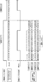
- FIG. 5 shows an example of the H-axis detection analog signal and the H-axis detection pulse signal according to the present embodiment.
- the H-axis detection analog signal is a waveform detected by one-side piezoelectric film (for example, 226a and 226b in FIG. 2 or 226a to 226d in FIG. 3) disposed in the horizontal scanner 220 that is driven on both sides in the horizontal direction. .
- the H-axis detection analog signal is an analog waveform corresponding to the direction of the MEMS mirror 224 of the horizontal scanner 220. For this reason, the H-axis detection analog signal cannot be processed by the FPGA 110 as it is. Therefore, in the present embodiment, the H-axis detection analog signal is converted into a pulsed rectangular wave using the comparator 170 or the like, and is input to the FPGA 110 as the H-axis detection pulse signal.
- the H-axis detection pulse signal is generated so that the edge comes to the position where the MEMS mirror 224 is swung by the maximum angle.
- the H-axis detection pulse signal is generated so as to repeat rising / falling for every minimum value (at the minimum peak) and maximum value (at the maximum peak) of the H-axis detection analog signal. Then, a horizontal drawing area is set in an area between edges sandwiched between edges of the H-axis pulse signal.
- an H-axis detection waveform (H-axis detection pulse signal) that is detected from the operation of the MEMS mirror 224 output from a detection circuit such as a piezoelectric film is taken into the FPGA 110 and the drawing timing is set. Used as a reference signal.
- the H-axis detection pulse signal also changes in the same manner. Since the FPGA 110 counts the edge interval of the H-axis detection pulse signal, the change in the frequency of the H-axis detection pulse signal causes a shift in the drawing timing due to a shift in the count number in the FPGA 110, and the projection to be drawn. This leads to a shift for each line of the image 300. In the present embodiment, this problem is improved as described below.
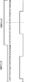
- FIGS. 6A and 6B show the operation of the reference example, which is an example having the same configuration as FIGS. 1 to 3 and FIG.
- the H-axis detection pulse signal always has a detection waveform with a constant period, that is, the same edge interval (interval between the rising edge and the next falling edge, the falling edge, This is a rectangular wave that repeats High / Low at an interval until the next rising edge).
- the FPGA 110 counts the edge interval of the H-axis detection pulse signal with an internal clock synchronized with the dot (pixel), and the H-axis detection pulse signal has a constant period, so the counter value of the clock counter (clk_cnt) is a constant value. It becomes.
- a counter value between 6 and 15 is set as a drawing area.
- HSync that sets the drawing area has a waveform that rises at the timing of the counter value 6 and repeats falling at the timing of the counter value 15 in each of the forward and return lines.
- the drawing area of the projection image 300 drawn by repeating the forward line and the backward line is the area A1.
- the H-axis detection pulse signal has a constant cycle and HSync also has a constant cycle
- the drawing position in the drawing area A1 is not shifted for each line, and the vertical vertical line is a straight line.
- FIGS. 7A and 7B show the operation of the reference example, which is an example having the same configuration as FIGS. 1 to 3 and FIG.
- the H-axis detection pulse signal when the operation of the MEMS mirror 224 is not constant, the H-axis detection pulse signal has a waveform in which the frequency (edge interval) is not constant but has changed.
- the counter value of the clock counter varies for each edge interval.
- the edge interval of the H-axis detection pulse signal is narrowed, so the counter value is small, and the MEMS mirror 224 is too much deviated from the ideal standard.
- the counter value becomes large.
- the forward line 1 is 20 counts
- the backward line 2 is 18 counts
- the forward line 3 is 22 counts
- the backward line 4 is 20 counts.
- the HSync for setting the drawing area rises at the timing of the counter value 6 for each of the forward and return lines where the edge interval (count number) varies, and the counter value 15 The waveform repeats falling at the timing.
- the drawing area of the projection image 300 drawn by repeating the forward line and the backward line is the area A2.
- the cycle (edge interval) of the H-axis detection pulse signal varies and the cycle of HSync also varies, so that the rendering position of the rendering area A2 is shifted for each line.
- the timing waveform (HSync) for drawing is generated and drawn on the basis of the counter value of the H-axis detection pulse signal, and drawing is performed when the count numbers in the forward line and the backward line are different. Deviation occurs in the vertical lines of the area.
- FIGS. 8A and 8B show the operation in the configuration of the present embodiment described with reference to FIGS.
- a line reference value serving as a reference for the edge interval (one line) of the H-axis detection pulse signal is set.
- a value calculated from the line reference value is used as a start counter value for starting counting on the next line. If the counter value is larger than the line reference value, the extra count is continued on the next line, or the count is stopped, and the count is started from the same position as the start position of the line reference value.
- the line reference value is an ideal deflection width of the MEMS mirror 224, and here, is an average value of counts (or counter values) obtained by counting a plurality of lines. For example, the edge interval of the H-axis detection pulse signal from the MEMS mirror 224 is counted in the blanking area before image data display, and the line reference value is set by averaging eight lines.
- FIGS. 7A and 7B show waveforms in which the frequency (edge interval) of the H-axis detection pulse signal is not constant, as in FIGS. 7A and 7B.
- the counter value of the clock counter clk_cnt
- a line reference value is set, and the start counter value is set so that the start count when moving to the next line is the same position as the line reference value count.
- the return line 2 has 18 counts, which is smaller than the line reference value of 20 counts, and the MEMS mirror 224 does not have enough deflection.
- the left end in the horizontal direction is shorter than the line reference value.
- the start counter value of line 3 is assumed.
- the interval from the edge of the next line to the drawing area is shortened by increasing the counter value based on the difference between the counter value and the line reference value.
- the counter values 6 to 15 of the return line 2 and the counter values 6 to 15 of the forward line 3 are equal in the vertical direction.
- the outbound line 3 has 22 counts, which is larger than the line reference value of 20 counts, and the MEMS mirror 224 is swung too much.
- the right end in the horizontal direction is longer than the line reference value.
- the interval from the edge of the next line to the drawing area is lengthened by delaying the start of counting based on the difference between the counter value and the line reference value.
- the counter values 6 to 15 of the forward path line 3 and the counter values 6 to 15 of the return path line 4 are equal to each other in the vertical direction.
- the counter value is not advanced during the count of the difference value, and after moving to the next line, the count value is stopped for 1 count for 4 counts of the stopped count value. Start counting from 1. Further, the counting may be continued without stopping until the counting is started on the next line.
- HSync for setting the drawing area rises at the timing of the corrected counter value 6 for each of the forward and return lines where the edge interval (count number) fluctuates, and the timing of the corrected counter value 15 The waveform repeats falling at.
- the drawing area of the projected image 300 drawn by repeating the forward line and the backward line is the area A3.
- the drawing area is controlled by controlling the count value based on the counter value as a reference and the count value from the detection pulse signal of the MEMS mirror so that the drawing areas match in the vertical line.
- the range can be kept constant, and vertical line shifts can be eliminated.
- the line reference value is determined by the average value obtained by counting a plurality of lines. For example, an average value of 8 lines in one frame is set as a line reference value. However, if the line reference value is an odd number, drawing deviation of one dot occurs. Therefore, it is preferable to determine that the line reference value is always an even number.
- FIG. 9 shows an example in which the line reference value is set to an odd number.
- FIG. 9 shows an example in which the line reference value is 21 and the area between the counter values 6 to 15 is a drawing area.
- the drawing area of the projection image 300 drawn by repeating the forward path line and the backward path line is the area A4.
- the line reference value is set to an odd number as shown in FIG. 9, the drawing position on the forward line (counter values 6 to 15) and the drawing position on the backward line (counter values 6 to 15) are shifted by one dot, and the forward path And the return path becomes alternate. For this reason, in this embodiment, the line reference value is always set to an even number to prevent the deviation between the forward path and the backward path. For example, when the average value is 21, the reference value is set to 20 or 22.
- FIG. 10 is an example of a functional block of the drawing position control unit 116
- FIG. 11 is an example of a flowchart of the drawing position control unit 116. Note that the operations in FIGS. 8A and 8B may be realized by other configurations.
- the drawing position control unit 116 includes a counter 11, a line reference value setting unit 12, a drawing position determination unit 13, a line deviation determination unit 14, and a line deviation correction unit 15.
- the counter 11 is a counter that counts the edge interval of the H-axis detection pulse signal.
- the counter 11 includes the clock counter and the pixel counter shown in FIGS. 8A and 8B.
- the line reference value setting unit 12 sets a line reference value to be a reference value for the counter of one line.
- the drawing position determination unit 13 determines a drawing position (drawing area) based on the value of the counter 11.
- the line deviation determination unit 14 compares the value of the counter 11 with the line reference value to determine line deviation.
- the line shift correction unit 15 corrects the start counter value and stops the counter as shown in FIGS. 8A and 8B.
- the line reference value setting unit 12 first sets a line reference value. As described above, after the counter 11 counts the edge interval of the H-axis detection pulse signal a plurality of times, the line reference value setting unit 12 obtains the average value of the counter values and sets the line reference value. In particular, the line reference value setting unit 12 sets the line reference value to be an even number as described above.
- the counter 11 counts the scanning range of the MEMS mirror (S103). In synchronization with the internal clock, the counter 11 counts the edge interval of the H-axis detection pulse signal by a clock counter (clk_cnt) and a pixel counter (pix_cnt) as shown in FIGS. 8A and 8B.
- a clock counter clk_cnt
- pix_cnt a pixel counter
- the drawing position determination unit 13 determines the drawing position based on the counter value. For example, the drawing position determination unit 13 sets between the counter values 5 to 14 as a drawing area, and generates HSync that rises at the timing of the counter value 5 and repeats the falling at the timing of the counter value 14.
- the line deviation determination unit 14 compares the counter value with the line reference value (S105). If the counter value is equal to the line reference value, there is no deviation in the line, so the count and the drawing position are determined as they are (S103, S104).
- the start counter value is set so as to correct the position of the drawing area based on the difference between the line reference value and the counter value as shown in FIGS. 8A and 8B (S106). . Thereafter, counting is started based on the set start counter value, and the drawing position is determined (S103, S104).
- the start of counting is waited so as to correct the position of the drawing area based on the difference between the counter value and the line reference value (S107). . Thereafter, the counting is started in accordance with the timing when there is no difference from the line reference value, and the drawing position is determined (S103, S104).
- the operation of the MEMS mirror is detected by the piezoelectric film provided in the optical scanner, and based on the deviation between the detected operation range and the reference range.
- the drawing position was corrected. Accordingly, the drawing position shift caused by the change in the detected waveform due to the fluctuation of the operation of the MEMS mirror is corrected, and the drawing shift for each line can be prevented by always setting the drawing area at a fixed location.
- the count value for setting the drawing position so as not to be always constant but constant with respect to the reference, it is possible to eliminate drawing position deviation for each line and prevent drawing deviation.
Abstract
画像表示装置(100)は、レーザー光を出力するRGBレーザーダイオード(200)と、レーザー光を反射し、水平方向に往復動作する水平スキャナ(220)と、水平方向のラインごとに動作範囲を検出する走査検出部(202)と、検出された動作範囲とライン基準値とのずれに基づいて、ラインごとに画像表示位置を決定する描画位置制御部(116)と、決定された画像表示位置に対応するタイミングで、画像データに基づきRGBレーザーダイオード(200)を駆動するレーザードライバ(140)と、を備える。
Description
本発明は、画像表示装置及びその制御方法に関し、より具体的には、レーザースキャン方式の画像表示装置及びその制御方法に関する。
レーザー光を反射させて走査することで画像を投影表示するレーザースキャン方式の画像表示装置が知られている(例えば、特許文献1)。レーザースキャン方式の画像表示装置は、自動車のウィンドシールドやコンバイナなどに画像を投影表示するHUD(Head Up Display)やプロジェクター等として利用されている。
レーザースキャン方式の画像表示装置では、ミラーを有する光スキャナによりレーザー光を反射させ、光スキャナのミラーを水平方向及び垂直方向に往復揺動させることで、レーザー光を走査している。
従来の画像表示装置では、光スキャナによるレーザー光の走査動作を制御するため、フィードバック制御が行われている。例えば、特許文献1では、光スキャナが反射した光を光センサで検出し、フィードバックを行っている。また、他の従来技術では、光スキャナに圧電膜を設けて、この圧電膜により光スキャナの動作を検出し、フィードバックすることも行われている。このような従来の画像表示装置のフィードバック制御では、走査周波数を一定に保つために、光スキャナを駆動する駆動信号の開始タイミングなどが制御されている。
しかしながら、振動や電気的な影響などにより光スキャナの往復動作が変動する場合があり、従来の画像表示装置では、この変動によって水平方向のラインなどの走査単位毎に画像がずれて表示される恐れがあるという問題がある。
そこで、本発明は、光束を出力する光源部と、前記光束を反射し、所定の走査方向に往復動作を繰り返す走査部と、前記往復動作の往路または復路の走査単位ごとに前記走査部の動作範囲を検出する走査検出部と、前記検出された動作範囲と基準範囲とのずれに基づいて、前記走査単位ごとに画像表示位置を決定する表示位置決定部と、前記決定された画像表示位置に対応するタイミングで、画像データに基づき前記光源部を駆動する光源駆動部と、を備える画像表示装置を提供する。
また、本発明は、光束を出力する光源部と、前記光束を反射し、所定の走査方向に往復動作を繰り返す走査部と、を備えた画像表示装置の制御方法であって、前記往復動作の往路または復路の走査単位ごとに前記走査部の動作範囲を検出し、前記検出された動作範囲と基準範囲とのずれに基づいて、前記走査単位ごとに画像表示位置を決定し、前記決定された画像表示位置に対応するタイミングで、画像データに基づき前記光源部を駆動する、画像表示装置の制御方法を提供する。
本発明によれば、走査単位毎の画像のずれを抑えることができる。
(実施の形態1)
以下、図面を参照して本発明の実施の形態1について説明する。
以下、図面を参照して本発明の実施の形態1について説明する。
図1は、本実施の形態に係る画像表示装置100の構成を示している。画像表示装置100は、レーザー光を光スキャナにより反射させ、垂直方向及び水平方向に往復走査することにより投影面に画像を表示(描画)するレーザースキャン方式の画像表示装置である。例えば、画像表示装置100は、自動車のウィンドシールドやコンバイナなど画像表示面である投影面に投影画像300を投影し表示する。
図1に示すように、画像表示装置100は、映像入力部101、FPGA(Field Programmable Gate Array)110、マイコン120、フラッシュメモリ131及び132、DDR(Double Data Rate)メモリ133、レーザードライバ140、V軸スキャナドライバ150、H軸スキャナドライバ160、コンパレータ170、RGBレーザーダイオード200、垂直スキャナ210、水平スキャナ220を備えている。なお、表示する画像の垂直方向(縦方向、Y方向)をV(Vertical)軸方向とも称し、画像の水平方向(横方向、X方向)をH(Horizontal)軸方向とも称する。
映像入力部101は、投影面に表示する映像データが入力され、入力された映像データはFPGA110に送出される。この映像データには、R(赤)G(緑)B(青)の3色の色信号が含まれている。例えば、映像入力部101は、カーナビゲーション装置など他の装置で生成された映像が入力されてもよいし、映像入力部101が映像データを生成してもよい。
FPGA110及びマイコン120は、画像表示装置100の制御部102を構成し、画像表示に必要な各種制御を行う。FPGA110及びマイコン120により、レーザードライバ140、V軸スキャナドライバ150、H軸スキャナドライバ160を介して、RGBレーザーダイオード200、垂直スキャナ210、水平スキャナ220の動作を制御し、投影画像300を描画する。なお、FPGA110及びマイコン120の制御動作は、ハードウェア又はソフトウェアのいずれか、もしくはその両方によって実現されてもよい。
FPGA110は、入力される映像データに基づいて、RGBの画像データを1ラインずつ出力し、また、垂直スキャナ210の往復動作を制御するためのV軸駆動信号を生成し、生成したV軸駆動信号を出力する。本実施の形態に係るFPGA110は、後述するように、コンパレータ170から得られる水平スキャナ220のH軸検出パルス信号に基づき、ライン毎の画像のずれを抑えるように画像の描画位置を設定し、設定した位置でレーザードライバ140を駆動させ描画を行う。
マイコン120は、水平スキャナ220の往復動作を制御するためのH軸駆動信号を生成し、生成したH軸駆動信号を出力する。フラッシュメモリ131及び132は、それぞれFPGA110及びマイコン120の動作に必要なデータやプログラムなどを記憶する不揮発性記憶部である。
DDR(Double Data Rate)メモリ133は、FPGA110に入力される映像データを一時的に保存するフレームバッファである。DDRメモリ133は、DDR2やDDR3、その他のSDRAMでもよい。
レーザードライバ140は、FPGA110から供給される画像データに応じて、RGBレーザーダイオード200を駆動する。レーザードライバ140は、FPGA110が決定した画像表示位置に対応するタイミングで、画像データに基づきRGBレーザーダイオード200を駆動する光源駆動部である。RGBレーザーダイオード200は、レーザードライバ140の駆動により、RGBの3色のレーザー光を発光する。RGBレーザーダイオード200は、光束であるレーザー光を出力する光源部である。
V軸スキャナドライバ150は、FPGA110から供給されるV軸駆動信号に応じて、垂直スキャナ210を往復駆動する。H軸スキャナドライバ160は、マイコン120から供給されるH軸駆動信号に応じて、水平スキャナ220を往復駆動する。
垂直スキャナ210または水平スキャナ220は、垂直または水平方向に往復動作を繰り返す走査部である。垂直スキャナ210は、RGBレーザーダイオード200から照射されたレーザー光を反射し、V軸スキャナドライバ150の駆動により垂直方向に往復動作する光スキャナである。水平スキャナ220は、RGBレーザーダイオード200から照射されたレーザー光を反射し、H軸スキャナドライバ160の駆動により水平方向に往復動作する光スキャナである。また、水平スキャナ220は、水平方向の往復動作を検出する走査検出部202を含み、検出した往復動作を示すH軸検出アナログ信号を出力する。走査検出部202は、往復動作の往路または復路のラインである走査単位ごとに水平スキャナ220の動作範囲を検出する。
この例では、水平スキャナ220が、RGBレーザーダイオード200からのレーザー光を反射し、垂直スキャナ210が、水平スキャナ220からの反射光をさらに反射することで、投影面へ投影画像300を描画している。垂直スキャナ210及び水平スキャナ220が、垂直方向及び水平方向に往復走査する光スキャナ201を構成しているとも言える。例えば、垂直スキャナ210と水平スキャナ220を1つの2軸(2次元)光スキャナとしてもよい。
コンパレータ170は、水平スキャナ220が出力したH軸検出アナログ信号を、FPGA110で処理可能なH軸検出パルス信号に変換する信号変換部である。
図2及び図3は、水平スキャナ220の構成例であり、水平スキャナ220をミラー側から見た正面図である。なお、垂直スキャナ210についても水平スキャナ220と同様に構成してもよい。
水平スキャナ220(及び垂直スキャナ210)である光スキャナは、MEMS(Micro Electro Mechanical Systems)技術により作成されたMEMS素子である。例えば、水平スキャナ220は、PZT(チタン酸ジルコン酸鉛)膜などの圧電膜を含むSOI(Silicon On Insulator)基板をエッチングして形成されている。
図2及び図3に示すように、水平スキャナ220は、本体の枠を構成する枠体221、枠体221の枠内において枠体221から離間した状態で支持された揺動片部222、枠体221の内縁と揺動片部222とを繋ぐ4つのL型梁部223a~223d、揺動片部222の表面に形成されたMEMSミラー224を備えている。MEMSミラー224は、反射率の高い金属(例えばAlやAu)を蒸着することにより形成されている。
L型梁部223a~223dは、揺動片部222の水平方向中央に近接した位置において揺動片部222と連結されており、この連結部を揺動軸として揺動片部222及びMEMSミラー224が水平方向に揺動可能となっている。L型梁部223a~223dは、揺動片部222を揺動可能に支持するトーションバーを構成しているとも言える。
さらに、4つL型梁部223a~233dにおいて、水平方向に延びる複数の圧電膜が配置されている。例えば、圧電膜は、下部電極と上部電極との間に圧電体膜を挟んだ積層構造である。
図2の例では、L型梁部223a及び223bに、H軸駆動信号が供給される駆動用圧電膜225a及び225bがそれぞれ配置され、L型梁部223a及び223bと対向するL型梁部223c及び223dに、MEMSミラー224(揺動片部222)の動作を検出する検出用圧電膜226a及び226bがそれぞれ配置されている。
また、図3の例では、L型梁部223a~223dに、駆動用圧電膜及び検出用圧電膜のペア(225a及び226a、225b及び226b、225c及び226c、225d及び226d)がそれぞれ配置されている。
図2の駆動用圧電膜225a及び225b、または図3の駆動用圧電膜225a~225dにH軸駆動信号を供給すると、H軸駆動信号に応じて駆動用圧電膜225a及び225b、または225a~225dが振動し、この振動がL型梁部223a及び223b、または223a~223dを介して揺動片部222に伝達され、揺動片部222及びMEMSミラー224が揺動する。
また図2の、検出用圧電膜226a及び226b、または図3の検出用圧電膜226a~226dは、走査検出部202であり、揺動片部222及びMEMSミラー224の振動を検出し、検出する振動に応じたH軸検出アナログ信号を出力する。検出用圧電膜226a及び226b、または226a~226dから得られるH軸検出アナログ信号に対して所定の位相差をもったH軸駆動信号を駆動用圧電膜225a及び225b、または225a~225dにフィードバックすることにより、揺動片部222及びMEMSミラー224を共振駆動させることができる。
図4は、本実施の形態に係るFPGA110の機能ブロックを示している。図4に示すように、FPGA110は、入力インタフェース111、DDRインタフェース112、画像処理部113、映像出力部114、PLL(Phase Locked Loop)115、描画位置制御部116、V軸駆動処理部117を備えている。
入力インタフェース111は、映像入力部101との間のインタフェースであり、映像入力部101から入力された映像データを受け取り、受け取った映像データをDDRインタフェース112へ出力する。
DDRインタフェース112は、DDRメモリ133との間のインタフェースであり、入力インタフェース111が受け取った映像データをDDRメモリ133に一時的に保存し、さらに、DDR133に保存した映像データを内部クロックに従って取り出す。
DDRインタフェース112は、DDRメモリ133へ映像データ(画像データ)をフレーム単位に書き込み、内部クロックと同期してDDRメモリ133から1フレームに含まれる水平方向の1ラインずつ読み出す。また、水平スキャナ220の往復動作における往路及び復路で描画を行うため、DDRインタフェース112は、往路で描画する往路ラインの場合、順方向のアドレス順に画像データを読み出し、復路で描画する復路ラインの場合、逆方向のアドレス順に画像データを読み出すことで、往路及び復路の画像データの並び替えを行う。
画像処理部113は、DDRインタフェース112がDDR133から取り出した画像データに対し、アスペクト比の変更やブライトコントロールなど、必要な画像処理を行う。映像出力部(画像出力部)114は、画像処理部113により画像処理された画像データをレーザードライバ140へ出力する。映像出力部114は、H軸検出波形とV軸駆動信号より生成された描画位置クロック(ピクセルクロック)、HSync(H軸同期信号)とVSync(V軸同期信号)を利用して描画位置を決定し、決定した描画位置のタイミングで、画像データを1ラインずつ出力する。
PLL115は、外部クロック180が入力され、この外部クロック180に基づいて内部クロックを生成し、生成した内部クロックを各ブロックへ供給する。
描画位置制御部(クロック生成部)116は、水平スキャナ220とレーザー描画の同期とるため、PLL115が生成した内部クロックに基づいて、ピクセルクロックを生成する。例えば、ピクセルクロックは、後述のピクセルカウンタに同期したクロックである。描画位置制御部116は、H軸検出パルス信号とV軸駆動信号に基づいて描画位置を決定するピクセルクロック、HSync、VSyncを生成する。描画位置制御部116は、H軸検出パルス信号のエッジ位置からカウンタのカウントを開始し、カウントしたカウンタ値により描画エリアを決定する。描画位置制御部116は、走査検出部202により検出された水平スキャナ220の動作範囲と基準範囲とのずれに基づいて、ラインごとに画像表示位置を決定する表示位置決定部である。
V軸駆動処理部117は、HSync及びVSyncに基づいてV軸駆動信号を生成し、生成したV軸駆動信号をV軸スキャナドライバ150へ出力する。例えば、VGA(Video Graphics Array)で表示する場合、垂直走査周波数は60Hzであり、60Hzで垂直スキャナ210を垂直方向に揺動させるようにV軸駆動信号を出力する。
図5は、本実施の形態に係るH軸検出アナログ信号及びH軸検出パルス信号の一例を示している。H軸検出アナログ信号は、水平方向の両側で駆動する水平スキャナ220に配置された片側の圧電膜(例えば、図2の226a及び226b、または図3の226a~226d)によって検出された波形である。
図5に示すように、H軸検出アナログ信号は、水平スキャナ220のMEMSミラー224の向きに応じたアナログ波形である。このため、そのままではFPGA110でH軸検出アナログ信号を処理することができない。そこで、本実施の形態では、コンパレータ170等を利用してH軸検出アナログ信号をパルス状の矩形波に変換し、H軸検出パルス信号としてFPGA110へ入力している。
本実施の形態では、MEMSミラー224が最大角度振った位置にエッジがくるようにH軸検出パルス信号を生成する。例えば、H軸検出アナログ信号の最小値(最小ピーク時)及び最大値(最大ピーク時)ごとに立ち上り/立ち下りを繰り返すようにH軸検出パルス信号を生成する。そして、H軸パルス信号のエッジに挟まれたエッジ間の領域に、水平方向の描画エリアを設定する。
次に、本実施の形態の主要な特徴である描画位置制御方法について説明する。
レーザースキャン方式の画像表示装置では、描画を行う時に、圧電膜などの検出回路から出力されるMEMSミラー224の動作を検出したH軸検出波形(H軸検出パルス信号)をFPGA110に取り込み描画タイミングの基準信号として利用をしている。
しかし、振動や電気的な影響によりMEMSミラー224の動作が変化した場合、H軸検出パルス信号も同様に変化する事になる。FPGA110では、H軸検出パルス信号のエッジ間隔をカウントしているため、このH軸検出パルス信号の周波数変化によって、FPGA110内のカウント数がずれる事で描画タイミングにずれが生じて、描画される投影画像300のライン毎のずれに繋がる。本実施の形態では、この問題を以下で説明するように改善する。
まず、図6A及び図6Bを用いて、MEMSミラーの動作が変化しない場合の理想的な検出パルス信号の動作について説明する。例えば、図6A及び図6Bは、参考例の動作であり、図1~図3、図5と同様の構成による例である。
図6A及び図6Bに示すように、理想的には、H軸検出パルス信号は常に一定周期の検出波形、すなわち、同じエッジ間隔(立ち上りエッジと次の立ち下りエッジまでの間隔、立ち下りエッジと次の立ち上りエッジまでの間隔)でHigh/Lowを繰り返す矩形波である。
FPGA110は、H軸検出パルス信号のエッジ間隔をドット(ピクセル)に同期した内部クロックでカウントしており、H軸検出パルス信号が一定周期のため、クロックカウンタ(clk_cnt)のカウンタ値は一定の値となる。ここでは、一例として、エッジ間隔を20カウントとし、カウンタ値=1~20が繰り返される。なお、説明簡略化のため、カウンタ値=1からカウントを開始するが、カウンタ値=0からカントを開始してもよい(以下でも同様)。
ここでは、一例として、カウンタ値6~15の間を描画エリアとして設定する。そうすると、描画エリアを設定するHSyncは、往路及び復路のラインのそれぞれでカウンタ値6のタイミングで立ち上り、カウンタ値15のタイミングで立ち下りを繰り返す波形となる。
その結果、この往路ライン及び復路ラインの繰り返しにより描画される投影画像300の描画エリアはA1の領域となる。図6A及び図6Bでは、H軸検出パルス信号が一定周期であり、HSyncも一定周期であるため、描画エリアA1は、ラインごとに描画位置がずれることはなく、垂直方向の縦ラインは一直線となる。
次に、図7A及び図7Bを用いて、本実施の形態の適用前の参考例における、MEMSミラーの動作が変化する場合の検出パルス信号の例について説明する。例えば、図7A及び図7Bは、参考例の動作であり、図1~図3、図5と同様の構成による例である。
図7A及び図7Bに示すように、MEMSミラー224の動作が一定ではない場合、H軸検出パルス信号は周波数(エッジ間隔)が一定ではなく変化した波形となる。このH軸検出パルス信号をFPGA110に取り込みエッジ間隔をカウントすると、エッジ間隔ごとにクロックカウンタのカウンタ値が変動する。
MEMSミラー224の振れが理想的な基準よりも足りない場合、H軸検出パルス信号のエッジ間隔が狭くなるため、カウンタ値が小さくなり、また、MEMSミラー224が理想的な基準よりも振れすぎた場合、H軸検出パルス信号のエッジ間隔が広くなるため、カウンタ値が大きくなる。例えば、往路ライン1は20カウント、復路ライン2は18カウント、往路ライン3は22カウント、復路ライン4は20カウントである。
カウンタ値6~15の間を描画エリアとして設定すると、描画エリアを設定するHSyncは、エッジ間隔(カウント数)が変動する往路及び復路のラインごとに、カウンタ値6のタイミングで立ち上り、カウンタ値15のタイミングで立ち下りを繰り返す波形となる。
その結果、この往路ライン及び復路ラインの繰り返しにより描画される投影画像300の描画エリアはA2の領域となる。図7A及び図7Bでは、H軸検出パルス信号の周期(エッジ間隔)が変動し、HSyncの周期も変動するため、描画エリアA2は、ラインごとに描画位置がずれてしまう。実施の形態適用前では、H軸検出パルス信号のカウンタ値を基準に描画するタイミング波形(HSync)を生成し描画を行っているため、往路ラインと復路ラインでのカウント数が異なった場合、描画エリアの縦のラインにずれが生じてしまう。
次に、図8A及び図8Bを用いて、本実施の形態の適用後における、MEMSミラーの動作が変化する場合の検出パルス信号の例について説明する。図8A及び図8Bは、図1~図5で説明した本実施の形態の構成における動作である。
本実施の形態では、H軸検出パルス信号のエッジ間隔(1ライン)の基準となるライン基準値を設定する。カウンタ値がライン基準値より小さい場合、次のラインでカウントを開始するスタートカウンタ値として、ライン基準値から算出した値を利用する。また、カウンタ値がライン基準値より大きい場合、余分にカウントした分を次のラインでもカウントを続け、または、カウントを停止し、ライン基準値のカウントのスタート位置と同じ位置からカウントをスタートする。
ライン基準値は、理想とするMEMSミラー224の振れ幅であり、ここでは、複数のラインをカウントしたカウント数(またはカウンタ値)の平均値である。例えば、画像データ表示前のブランキングエリア内でMEMSミラー224からのH軸検出パルス信号のエッジ間隔をカウントし、8ライン分を平均してライン基準値を設定する。
例えば、1ライン=20カウント、2ライン=18カウント、3ライン=22カウント、4ライン=20カウント、5ライン=18カウント、6ライン=20カウント、7ライン=20カウント、9ライン=22カウントの場合、平均値である20カウントを1フレーム内のライン基準値とする。そして、10ライン以降は、このライン基準値に基づいてカウンタ値を設定する。
図8A及び図8Bでは、図7A及び図7Bと同様に、H軸検出パルス信号の周波数(エッジ間隔)が一定ではなく変化した波形となっている。このH軸検出パルス信号のエッジ間隔を内部クロックに合わせてカウントすると、エッジ間隔ごとにクロックカウンタ(clk_cnt)のカウンタ値が変動する。このため、本実施の形態では、ライン基準値を設定し、次のラインに移った時のスタートカウントがライン基準値のカウントと同じ位置となるように、スタートカウンタ値を設定する。
H軸検出パルス信号を常にカウンタ値=1からカウントするクロックをクロックカウンタ(clk_cnt)と称し、ライン基準値に基づいて設定されたスタートカウンタ値からカウントするクロックをピクセルカウンタ(pix_cnt)と称する。
図8A及び図8Bでは、図7A及び図7Bと同様に、例えば、往路ライン1は20カウント(clk_cnt=1~20)、復路ライン2は18カウント(clk_cnt=1~18)、往路ライン3は22カウント(clk_cnt=1~22)、復路ライン4は20カウント(clk_cnt=1~20)である。
MEMSミラー224の振れが基準値よりも足りない例として、例えば、復路ライン2では、18カウントのため、ライン基準値の20カウントよりも小さく、MEMSミラー224の振れが足りない。この例では、水平方向の左端がライン基準値よりも短い。この場合、ライン基準値の20カウントからピクセルカウンタのカウンタ値(pix_cnt=18)を差し引いて差分値(20-18=2)を求める。次のラインでは、この差分値のドット分(基準値より不足した分)だけタイミングをずらすために、カウンタの最小値=1にこの差分値を加えた値(1+2=3)を、次の往路ライン3のスタートカウンタ値とする。すなわち、カウンタ値がライン基準値よりも小さい場合、カウンタ値とライン基準値との差分に基づいてカウンタ値を増加させることで、次のラインのエッジから描画エリアまでの間隔を短くする。これにより、復路ライン2のカウンタ値6~15と、往路ライン3のカウンタ値6~15とで、垂直方向の位置が等しくなる。
また、MEMSミラー224が基準値よりも振れすぎている例として、往路ライン3では、22カウントのため、ライン基準値の20カウントよりも大きく、MEMSミラー224が振れすぎている。この例では、水平方向の右端がライン基準値よりも長い。この場合、ピクセルカウンタがエッジまでカウントしたカウンタ値(pix_cnt=24)からライン基準値の20カウントを差し引いて差分値(24-20=4)を求める。次のラインでは、この差分値のドット分(基準値を超えた分)だけタイミングをずらすために、次の復路ライン4で、差分値のカウント分の次の位置(4+1=5カウント目)からカウントを開始する。すなわち、カウンタ値がライン基準値よりも大きい場合、カウンタ値とライン基準値との差分に基づいてカウントの開始を遅らせることで、次のラインのエッジから描画エリアまでの間隔を長くする。これにより、往路ライン3のカウンタ値6~15と、復路ライン4のカウンタ値6~15とで、垂直方向の位置が等しくなる。
例えば、このとき、差分値のカウント分の間はカウンタ値を進めず、次のラインに移ってからも、止めたカウント値の4カウント分、カウント値を1のままで停止した後、通常のカウントを1から始める。また、次のラインでカウントを開始するまで、カウンタを止めずにカウントし続けてもよい。
このような制御により、描画エリアを設定するHSyncは、エッジ間隔(カウント数)が変動する往路及び復路のラインごとに、補正されたカウンタ値6のタイミングで立ち上り、補正されたカウンタ値15のタイミングで立ち下りを繰り返す波形となる。
その結果、この往路ライン及び復路ラインの繰り返しにより描画される投影画像300の描画エリアはA3の領域となる。図8A及び図8Bでは、H軸検出パルス信号のエッジ間隔と基準値との差分に基づいてカウンタを制御することにより、先のラインの描画エリアから終端までの距離と、次のラインの先頭から描画エリアまでの距離を等しくできる。すなわち、本実施の形態では、縦のラインにおいて描画エリアが一致するように、基準とするカウンタ値とMEMSミラーの検出パルス信号からのカウント値に基づいて、カウント値を制御する事で、描画エリア範囲を一定に保つ事ができ、縦ラインのずれを無くす事ができる。
ここで、ライン基準値の設定値についてさらに説明する。上記では、複数のラインをカウントした平均値によりライン基準値を決定した。例えば、1フレーム内の8ラインの平均値をライン基準値とした。しかし、ライン基準値が奇数であると、1ドットの描画ずれが起きてしまう為、ライン基準値は常に偶数になるよう決定することが好ましい。
図9は、ライン基準値を奇数に設定した例を示している。図9は、ライン基準値を21とし、カウンタ値6~15の間を描画エリアとした例である。この場合、往路ライン及び復路ラインの繰り返しにより描画される投影画像300の描画エリアはA4の領域となる。
図9のように、ライン基準値を奇数に設定すると、往路ラインにおける描画位置(カウンタ値6~15)と、復路ラインにおける描画位置(カウンタ値6~15)とが1ドットずれてしまい、往路と復路が互い違いになってしまう。このため、本実施の形態では、ライン基準値を常に偶数に設定することで、往路と復路のずれを防止する。例えば、平均値が21の場合、基準値を20または22に設定する。
次に、図8A及び図8Bで説明した、本実施の形態の動作を実現するための構成例について説明する。図10は、描画位置制御部116の機能ブロックの一例であり、図11は描画位置制御部116のフローチャートの一例である。なお、その他の構成により図8A及び図8Bの動作を実現してもよい。
図10に示すように、描画位置制御部116は、カウンタ11、ライン基準値設定部12、描画位置決定部13、ラインずれ判定部14、ラインずれ補正部15を備えている。
カウンタ11は、H軸検出パルス信号のエッジ間隔をカウントするカウンタである。カウンタ11は、図8A及び図8Bのクロックカウンタ及びピクセルカウンタを含んでいる。ライン基準値設定部12、1ラインのカウンタの基準値となるライン基準値を設定する。
描画位置決定部13は、カウンタ11の値に基づいて、描画位置(描画エリア)を決定する。ラインずれ判定部14、カウンタ11の値とライン基準値とを比較しラインのずれを判定する。ラインずれ補正部15、判定されたラインのずれを補正するため、図8A及び図8Bのようにスタートカウンタ値を補正やカウンタの停止を行う。
図11に示すように、描画位置制御部116に、H軸検出パルス信号の入力が開始されると(S101)、まず、ライン基準値設定部12がライン基準値を設定する。上記のように、カウンタ11がH軸検出パルス信号のエッジ間隔を複数回カウントした後、ライン基準値設定部12は、カウンタ値の平均値を求めてライン基準値を設定する。特に、ライン基準値設定部12は、上記のようにライン基準値が偶数となるように設定する。
続いて、カウンタ11は、MEMSミラーの走査範囲をカウントする(S103)。カウンタ11は、内部クロックに同期して、図8A及び図8Bのように、クロックカウンタ(clk_cnt)、ピクセルカウンタ(pix_cnt)により、H軸検出パルス信号のエッジ間隔をカウントする。
続いて、描画位置決定部13は、カウンタ値に基づいて描画位置を決定する。例えば、描画位置決定部13は、カウンタ値5~14の間を描画エリアとして設定し、カウンタ値5のタイミングで立ち上り、カウンタ値14のタイミングで立ち下りを繰り返すHSyncを生成する。
続いて、ラインずれ判定部14は、カウンタ値とライン基準値とを比較する(S105)。カウンタ値とライン基準値とが等しい場合は、ラインにずれは無いため、そのままカウント及び描画位置決定を行う(S103、S104)。
カウンタ値がライン基準値よりも小さい場合、図8A及び図8Bのように、ライン基準値とカウンタ値の差分に基づいて、描画エリアの位置を補正するようにスタートカウンタ値を設定する(S106)。その後、設定したスタートカウンタ値により、カウントを開始し、描画位置を決定する(S103、S104)。
カウンタ値がライン基準値よりも大きい場合、図8A及び図8Bのように、カウンタ値とライン基準値との差分に基づいて、描画エリアの位置を補正するようにカウントの開始を待つ(S107)。その後、ライン基準値と差がない場合のタイミングに合わせて、カウントを開始し、描画位置を決定する(S103、S104)。
以上のように、本実施の形態では、レーザースキャン方式の画像表示装置において、光スキャナに設けられた圧電膜によりMEMSミラーの動作を検出し、この検出した動作範囲と基準範囲とのずれに基づいて、描画位置を補正することとした。これにより、MEMSミラーの動作変動による検出波形の変化がもたらす描画位置のずれを補正し、常に一定の場所に描画エリアを設定する事でライン毎の描画ずれを防止することができる。特に、描画位置を設定するカウント値を常に一定ではなく、基準に対して一定になるように設定することで、ライン毎の描画位置のずれを無くし、描画ずれを防止することができる。
なお、本発明は上記実施の形態に限られたものではなく、趣旨を逸脱しない範囲で適宜変更することが可能である。
この出願は、2013年12月17日に出願された日本出願特願2013-260396を基礎とする優先権を主張し、その開示の全てをここに取り込む。
11 カウンタ
12 ライン基準値設定部
13 描画位置決定部
14 ラインずれ判定部
15 ラインずれ補正部
100 画像表示装置
101 映像入力部
111 入力インタフェース
112 DDRインタフェース
113 画像処理部
114 映像出力部
116 描画位置制御部
117 V軸駆動処理部
120 マイコン
131、132 フラッシュメモリ
133 DDRメモリ
140 レーザードライバ
150 V軸スキャナドライバ
160 H軸スキャナドライバ
170 コンパレータ
180 外部クロック
200 RGBレーザーダイオード
201 光スキャナ
202 走査検出部
210 垂直スキャナ
220 水平スキャナ
221 枠体
222 揺動片部
223a~223d L型梁部
224 MEMSミラー
225a~225d 駆動用圧電膜
226a~226d 検出用圧電膜
300 投影画像
Claims (8)
- 光束を出力する光源部と、
前記光束を反射し、所定の走査方向に往復動作を繰り返す走査部と、
前記往復動作の往路または復路の走査単位ごとに前記走査部の動作範囲を検出する走査検出部と、
前記検出された動作範囲と基準範囲とのずれに基づいて、前記走査単位ごとに画像表示位置を決定する表示位置決定部と、
前記決定された画像表示位置に対応するタイミングで、画像データに基づき前記光源部を駆動する光源駆動部と、
を備える画像表示装置。 - 前記表示位置決定部は、前記検出された動作範囲が前記基準範囲よりも小さい場合、前記検出された動作範囲と前記基準範囲との差分に基づいて、次の走査単位における前記走査部の動作開始から前記画像表示位置までの間隔を小さくする、
請求項1に記載の画像表示装置。 - 前記検出された動作範囲をクロックに基づいてカウントするカウンタを備え、
前記表示位置決定部は、前記検出された動作範囲を前記カウンタがカウントしたカウンタ値と前記基準範囲に対応するカウンタ値との差分に基づき、次の走査単位における前記カウンタの開始カウント値を増加させる、
請求項2に記載の画像表示装置。 - 前記表示位置決定部は、前記検出された動作範囲が前記基準範囲よりも大きい場合、前記検出された動作範囲と前記基準範囲との差分に基づいて、次の走査単位における前記走査部の動作開始から前記画像表示位置までの間隔を大きくする、
請求項1または2に記載の画像表示装置。 - 前記検出された動作範囲をクロックに基づいてカウントするカウンタを備え、
前記表示位置決定部は、前記検出された動作範囲を前記カウンタがカウントしたカウンタ値と前記基準範囲に対応するカウンタ値との差分に基づき、次の走査単位における前記カウンタのカウント開始を遅らせる、
請求項4に記載の画像表示装置。 - 前記表示位置決定部は、前記検出された複数の動作範囲の平均に基づいて前記基準範囲を設定する、
請求項1乃至5のいずれか一項に記載の画像表示装置。 - 前記表示位置決定部は、前記動作範囲をクロックに基づいてカウントしたときに偶数となるように、前記基準範囲を設定する、
請求項1乃至6のいずれか一項に記載の画像表示装置。 - 光束を出力する光源部と、前記光束を反射し、所定の走査方向に往復動作を繰り返す走査部と、を備えた画像表示装置の制御方法であって、
前記往復動作の往路または復路の走査単位ごとに前記走査部の動作範囲を検出し、
前記検出された動作範囲と基準範囲とのずれに基づいて、前記走査単位ごとに画像表示位置を決定し、
前記決定された画像表示位置に対応するタイミングで、画像データに基づき前記光源部を駆動する、
画像表示装置の制御方法。
Priority Applications (2)
| Application Number | Priority Date | Filing Date | Title |
|---|---|---|---|
| EP14870909.0A EP3086548B1 (en) | 2013-12-17 | 2014-07-01 | Image display device and control method for same |
| US15/173,282 US20160286185A1 (en) | 2013-12-17 | 2016-06-03 | Image display device and control method thereof |
Applications Claiming Priority (2)
| Application Number | Priority Date | Filing Date | Title |
|---|---|---|---|
| JP2013-260396 | 2013-12-17 | ||
| JP2013260396A JP6090147B2 (ja) | 2013-12-17 | 2013-12-17 | 画像表示装置及びその制御方法 |
Related Child Applications (1)
| Application Number | Title | Priority Date | Filing Date |
|---|---|---|---|
| US15/173,282 Continuation US20160286185A1 (en) | 2013-12-17 | 2016-06-03 | Image display device and control method thereof |
Publications (1)
| Publication Number | Publication Date |
|---|---|
| WO2015092948A1 true WO2015092948A1 (ja) | 2015-06-25 |
Family
ID=53402339
Family Applications (1)
| Application Number | Title | Priority Date | Filing Date |
|---|---|---|---|
| PCT/JP2014/003493 WO2015092948A1 (ja) | 2013-12-17 | 2014-07-01 | 画像表示装置及びその制御方法 |
Country Status (4)
| Country | Link |
|---|---|
| US (1) | US20160286185A1 (ja) |
| EP (1) | EP3086548B1 (ja) |
| JP (1) | JP6090147B2 (ja) |
| WO (1) | WO2015092948A1 (ja) |
Cited By (1)
| Publication number | Priority date | Publication date | Assignee | Title |
|---|---|---|---|---|
| WO2016075854A1 (ja) * | 2014-11-10 | 2016-05-19 | 株式会社Jvcケンウッド | 画像表示装置及びその制御方法 |
Families Citing this family (7)
| Publication number | Priority date | Publication date | Assignee | Title |
|---|---|---|---|---|
| JP6978659B2 (ja) * | 2016-12-21 | 2021-12-08 | ミツミ電機株式会社 | 画像投影装置および補償方法 |
| JP6350685B2 (ja) * | 2017-01-20 | 2018-07-04 | 株式会社Jvcケンウッド | 画像表示装置及びその制御方法 |
| JP6365698B2 (ja) * | 2017-01-20 | 2018-08-01 | 株式会社Jvcケンウッド | 画像表示装置及びその制御方法 |
| DE102017218670A1 (de) * | 2017-10-19 | 2019-04-25 | Robert Bosch Gmbh | Mikromechanische Mikrospiegelanordnung und entsprechendes Betriebsverfahren |
| JP7025634B2 (ja) * | 2017-11-01 | 2022-02-25 | ミツミ電機株式会社 | 画像投影装置及び画像投影方法 |
| JP6753449B2 (ja) | 2017-11-24 | 2020-09-09 | 株式会社村田製作所 | 走査反射器システム |
| JP6870699B2 (ja) * | 2018-05-03 | 2021-05-12 | 株式会社村田製作所 | 拡大された画像領域を備える走査光学デバイス |
Citations (4)
| Publication number | Priority date | Publication date | Assignee | Title |
|---|---|---|---|---|
| JP2007025522A (ja) | 2005-07-21 | 2007-02-01 | Seiko Epson Corp | 画像表示装置及び画像表示装置の制御方法 |
| JP2010266824A (ja) * | 2009-05-18 | 2010-11-25 | Seiko Epson Corp | 画像表示装置 |
| JP2013072982A (ja) * | 2011-09-27 | 2013-04-22 | Nec Corp | 蛍光体スクリーンおよびそれを用いた走査型表示装置 |
| WO2013100066A1 (ja) * | 2011-12-28 | 2013-07-04 | 株式会社Jvcケンウッド | 画像表示装置、画像表示装置の制御方法、および、情報出力装置 |
Family Cites Families (6)
| Publication number | Priority date | Publication date | Assignee | Title |
|---|---|---|---|---|
| JP3265854B2 (ja) * | 1994-09-28 | 2002-03-18 | ミノルタ株式会社 | 画像出力装置 |
| US7302174B2 (en) * | 2003-12-31 | 2007-11-27 | Symbol Technologies, Inc. | Method and apparatus for capturing images using a color laser projection display |
| US20070115440A1 (en) * | 2005-11-21 | 2007-05-24 | Microvision, Inc. | Projection display with screen compensation |
| US20080001850A1 (en) * | 2006-06-06 | 2008-01-03 | Mark Champion | Beam scanner with reduced phase error |
| US8842352B2 (en) * | 2006-08-17 | 2014-09-23 | Texas Instruments Incorporated | Method to improve scan-line alignment by adjusting the pixel rate |
| JP5393043B2 (ja) * | 2008-03-14 | 2014-01-22 | キヤノン株式会社 | 画像表示装置、画像表示方法 |
-
2013
- 2013-12-17 JP JP2013260396A patent/JP6090147B2/ja active Active
-
2014
- 2014-07-01 WO PCT/JP2014/003493 patent/WO2015092948A1/ja active Application Filing
- 2014-07-01 EP EP14870909.0A patent/EP3086548B1/en active Active
-
2016
- 2016-06-03 US US15/173,282 patent/US20160286185A1/en not_active Abandoned
Patent Citations (4)
| Publication number | Priority date | Publication date | Assignee | Title |
|---|---|---|---|---|
| JP2007025522A (ja) | 2005-07-21 | 2007-02-01 | Seiko Epson Corp | 画像表示装置及び画像表示装置の制御方法 |
| JP2010266824A (ja) * | 2009-05-18 | 2010-11-25 | Seiko Epson Corp | 画像表示装置 |
| JP2013072982A (ja) * | 2011-09-27 | 2013-04-22 | Nec Corp | 蛍光体スクリーンおよびそれを用いた走査型表示装置 |
| WO2013100066A1 (ja) * | 2011-12-28 | 2013-07-04 | 株式会社Jvcケンウッド | 画像表示装置、画像表示装置の制御方法、および、情報出力装置 |
Cited By (3)
| Publication number | Priority date | Publication date | Assignee | Title |
|---|---|---|---|---|
| WO2016075854A1 (ja) * | 2014-11-10 | 2016-05-19 | 株式会社Jvcケンウッド | 画像表示装置及びその制御方法 |
| JP2016090913A (ja) * | 2014-11-10 | 2016-05-23 | 株式会社Jvcケンウッド | 画像表示装置及びその制御方法 |
| EP3220184A4 (en) * | 2014-11-10 | 2017-12-13 | JVC Kenwood Corporation | Image display device and control method therefor |
Also Published As
| Publication number | Publication date |
|---|---|
| EP3086548B1 (en) | 2019-10-16 |
| JP6090147B2 (ja) | 2017-03-08 |
| EP3086548A1 (en) | 2016-10-26 |
| JP2015118181A (ja) | 2015-06-25 |
| EP3086548A4 (en) | 2016-12-21 |
| US20160286185A1 (en) | 2016-09-29 |
Similar Documents
| Publication | Publication Date | Title |
|---|---|---|
| JP6090147B2 (ja) | 画像表示装置及びその制御方法 | |
| US9894335B2 (en) | Image display device and control method thereof | |
| US7864390B2 (en) | Image display apparatus | |
| US7436567B2 (en) | Optical scanner and scanning type projector | |
| US9251730B2 (en) | Image display apparatus and image scanning apparatus | |
| US20100079683A1 (en) | Display apparatus | |
| US20110051210A1 (en) | Laser Projector | |
| US9075246B2 (en) | Image display device having laser light scanning with a variation in scanning speed | |
| JP2006323355A (ja) | 光走査装置、光走査装置の制御方法及び画像表示装置 | |
| WO2013100066A1 (ja) | 画像表示装置、画像表示装置の制御方法、および、情報出力装置 | |
| WO2014103462A1 (ja) | 画像表示装置、画像表示方法及びプログラム | |
| EP3349441A2 (en) | Image projection apparatus and compensation method | |
| KR20140000667A (ko) | 화상 표시 장치 | |
| JP6365698B2 (ja) | 画像表示装置及びその制御方法 | |
| JP6350685B2 (ja) | 画像表示装置及びその制御方法 | |
| JPWO2013047656A1 (ja) | 画像投影装置および光軸ずれ補正方法 | |
| US20170248781A1 (en) | Image drawing device and image drawing method | |
| JP6946708B2 (ja) | 制御装置、画像投影装置、および制御方法 | |
| JP2014010347A (ja) | 画像表示装置および画像表示方法 | |
| JP2010266824A (ja) | 画像表示装置 | |
| JP2015040928A (ja) | 光偏向装置、画像形成装置、車両及び光偏向装置の制御方法 | |
| EP3264401B1 (en) | Image rendering device, head-up display, and method for adjusting image luminance | |
| JP7396147B2 (ja) | 可動装置、光偏向装置、画像投影装置、光書込装置、物体認識装置、移動体、ヘッドマウントディスプレイ | |
| JP2007057556A (ja) | 画像表示装置及び画像表示装置の制御方法 |
Legal Events
| Date | Code | Title | Description |
|---|---|---|---|
| 121 | Ep: the epo has been informed by wipo that ep was designated in this application |
Ref document number: 14870909 Country of ref document: EP Kind code of ref document: A1 |
|
| REEP | Request for entry into the european phase |
Ref document number: 2014870909 Country of ref document: EP |
|
| WWE | Wipo information: entry into national phase |
Ref document number: 2014870909 Country of ref document: EP |
|
| NENP | Non-entry into the national phase |
Ref country code: DE |