WO2015087861A1 - 蛍光体、およびその製造方法、ならびにその蛍光体を用いた発光装置 - Google Patents
蛍光体、およびその製造方法、ならびにその蛍光体を用いた発光装置 Download PDFInfo
- Publication number
- WO2015087861A1 WO2015087861A1 PCT/JP2014/082516 JP2014082516W WO2015087861A1 WO 2015087861 A1 WO2015087861 A1 WO 2015087861A1 JP 2014082516 W JP2014082516 W JP 2014082516W WO 2015087861 A1 WO2015087861 A1 WO 2015087861A1
- Authority
- WO
- WIPO (PCT)
- Prior art keywords
- phosphor
- light emitting
- light
- emitting device
- fluorescent substance
- Prior art date
Links
- 238000000034 method Methods 0.000 title claims abstract description 15
- 239000000126 substance Substances 0.000 title abstract description 10
- 230000008569 process Effects 0.000 title abstract description 3
- 238000006243 chemical reaction Methods 0.000 claims abstract description 36
- KRHYYFGTRYWZRS-UHFFFAOYSA-N Fluorane Chemical compound F KRHYYFGTRYWZRS-UHFFFAOYSA-N 0.000 claims abstract description 29
- 229910000040 hydrogen fluoride Inorganic materials 0.000 claims abstract description 23
- 229910018672 Mn—F Inorganic materials 0.000 claims abstract description 18
- 238000001237 Raman spectrum Methods 0.000 claims abstract description 17
- 229910008284 Si—F Inorganic materials 0.000 claims abstract description 15
- 239000013078 crystal Substances 0.000 claims abstract description 15
- 239000012286 potassium permanganate Substances 0.000 claims abstract description 14
- 229910052710 silicon Inorganic materials 0.000 claims abstract description 12
- XUIMIQQOPSSXEZ-UHFFFAOYSA-N Silicon Chemical compound [Si] XUIMIQQOPSSXEZ-UHFFFAOYSA-N 0.000 claims abstract description 11
- 239000010703 silicon Substances 0.000 claims abstract description 11
- 238000001069 Raman spectroscopy Methods 0.000 claims abstract description 9
- 239000000203 mixture Substances 0.000 claims abstract description 8
- OAICVXFJPJFONN-UHFFFAOYSA-N Phosphorus Chemical class [P] OAICVXFJPJFONN-UHFFFAOYSA-N 0.000 claims description 146
- 229910052791 calcium Inorganic materials 0.000 claims description 15
- 229910052712 strontium Inorganic materials 0.000 claims description 15
- 229910052788 barium Inorganic materials 0.000 claims description 12
- 238000004519 manufacturing process Methods 0.000 claims description 12
- 229910052688 Gadolinium Inorganic materials 0.000 claims description 4
- 229910004283 SiO 4 Inorganic materials 0.000 claims description 4
- 239000000758 substrate Substances 0.000 claims description 4
- 229910052727 yttrium Inorganic materials 0.000 claims description 4
- 102100032047 Alsin Human genes 0.000 claims description 2
- 101710187109 Alsin Proteins 0.000 claims description 2
- 229910052693 Europium Inorganic materials 0.000 claims description 2
- 229910052772 Samarium Inorganic materials 0.000 claims description 2
- 229910052733 gallium Inorganic materials 0.000 claims description 2
- 229910052746 lanthanum Inorganic materials 0.000 claims description 2
- 229910021417 amorphous silicon Inorganic materials 0.000 claims 1
- 229910021486 amorphous silicon dioxide Inorganic materials 0.000 claims 1
- 229910021488 crystalline silicon dioxide Inorganic materials 0.000 claims 1
- 229910021421 monocrystalline silicon Inorganic materials 0.000 claims 1
- 229910021420 polycrystalline silicon Inorganic materials 0.000 claims 1
- 239000011572 manganese Substances 0.000 description 29
- 239000000243 solution Substances 0.000 description 23
- 239000004065 semiconductor Substances 0.000 description 14
- 239000002245 particle Substances 0.000 description 13
- VYPSYNLAJGMNEJ-UHFFFAOYSA-N Silicium dioxide Chemical compound O=[Si]=O VYPSYNLAJGMNEJ-UHFFFAOYSA-N 0.000 description 12
- 239000010410 layer Substances 0.000 description 11
- 229910052748 manganese Inorganic materials 0.000 description 11
- 239000000463 material Substances 0.000 description 10
- PWHULOQIROXLJO-UHFFFAOYSA-N Manganese Chemical compound [Mn] PWHULOQIROXLJO-UHFFFAOYSA-N 0.000 description 9
- QVGXLLKOCUKJST-UHFFFAOYSA-N atomic oxygen Chemical compound [O] QVGXLLKOCUKJST-UHFFFAOYSA-N 0.000 description 7
- 239000011575 calcium Substances 0.000 description 7
- 230000005284 excitation Effects 0.000 description 7
- 238000005259 measurement Methods 0.000 description 7
- 239000001301 oxygen Substances 0.000 description 7
- 229910052760 oxygen Inorganic materials 0.000 description 7
- 239000002344 surface layer Substances 0.000 description 7
- 230000008859 change Effects 0.000 description 6
- 230000007423 decrease Effects 0.000 description 6
- CNQCVBJFEGMYDW-UHFFFAOYSA-N lawrencium atom Chemical compound [Lr] CNQCVBJFEGMYDW-UHFFFAOYSA-N 0.000 description 6
- 229910052700 potassium Inorganic materials 0.000 description 6
- 239000000377 silicon dioxide Substances 0.000 description 6
- ZLMJMSJWJFRBEC-UHFFFAOYSA-N Potassium Chemical compound [K] ZLMJMSJWJFRBEC-UHFFFAOYSA-N 0.000 description 5
- 239000011591 potassium Substances 0.000 description 5
- 239000011230 binding agent Substances 0.000 description 4
- 230000015572 biosynthetic process Effects 0.000 description 4
- 230000000694 effects Effects 0.000 description 4
- 239000011159 matrix material Substances 0.000 description 4
- 229910052751 metal Inorganic materials 0.000 description 4
- 238000003786 synthesis reaction Methods 0.000 description 4
- 230000009102 absorption Effects 0.000 description 3
- 238000010521 absorption reaction Methods 0.000 description 3
- 239000007864 aqueous solution Substances 0.000 description 3
- 238000000576 coating method Methods 0.000 description 3
- 230000000052 comparative effect Effects 0.000 description 3
- 238000004993 emission spectroscopy Methods 0.000 description 3
- 238000000295 emission spectrum Methods 0.000 description 3
- 229910052731 fluorine Inorganic materials 0.000 description 3
- 239000011737 fluorine Substances 0.000 description 3
- 238000002844 melting Methods 0.000 description 3
- 239000002184 metal Substances 0.000 description 3
- 229920005989 resin Polymers 0.000 description 3
- 239000011347 resin Substances 0.000 description 3
- 229920002050 silicone resin Polymers 0.000 description 3
- YCKRFDGAMUMZLT-UHFFFAOYSA-N Fluorine atom Chemical compound [F] YCKRFDGAMUMZLT-UHFFFAOYSA-N 0.000 description 2
- BPQQTUXANYXVAA-UHFFFAOYSA-N Orthosilicate Chemical compound [O-][Si]([O-])([O-])[O-] BPQQTUXANYXVAA-UHFFFAOYSA-N 0.000 description 2
- UCKMPCXJQFINFW-UHFFFAOYSA-N Sulphide Chemical compound [S-2] UCKMPCXJQFINFW-UHFFFAOYSA-N 0.000 description 2
- BOTDANWDWHJENH-UHFFFAOYSA-N Tetraethyl orthosilicate Chemical compound CCO[Si](OCC)(OCC)OCC BOTDANWDWHJENH-UHFFFAOYSA-N 0.000 description 2
- 239000004110 Zinc silicate Substances 0.000 description 2
- YKTSYUJCYHOUJP-UHFFFAOYSA-N [O--].[Al+3].[Al+3].[O-][Si]([O-])([O-])[O-] Chemical compound [O--].[Al+3].[Al+3].[O-][Si]([O-])([O-])[O-] YKTSYUJCYHOUJP-UHFFFAOYSA-N 0.000 description 2
- 238000004458 analytical method Methods 0.000 description 2
- 239000011248 coating agent Substances 0.000 description 2
- 239000003822 epoxy resin Substances 0.000 description 2
- 125000001153 fluoro group Chemical group F* 0.000 description 2
- 239000011521 glass Substances 0.000 description 2
- 238000005286 illumination Methods 0.000 description 2
- 229910010272 inorganic material Inorganic materials 0.000 description 2
- 239000011147 inorganic material Substances 0.000 description 2
- 230000010354 integration Effects 0.000 description 2
- 238000005342 ion exchange Methods 0.000 description 2
- 239000004973 liquid crystal related substance Substances 0.000 description 2
- 230000008018 melting Effects 0.000 description 2
- 238000002156 mixing Methods 0.000 description 2
- 239000011368 organic material Substances 0.000 description 2
- 229920000647 polyepoxide Polymers 0.000 description 2
- 239000000843 powder Substances 0.000 description 2
- 238000006862 quantum yield reaction Methods 0.000 description 2
- 238000010791 quenching Methods 0.000 description 2
- 230000000171 quenching effect Effects 0.000 description 2
- 239000002994 raw material Substances 0.000 description 2
- 238000009877 rendering Methods 0.000 description 2
- 238000001228 spectrum Methods 0.000 description 2
- XSMMCTCMFDWXIX-UHFFFAOYSA-N zinc silicate Chemical compound [Zn+2].[O-][Si]([O-])=O XSMMCTCMFDWXIX-UHFFFAOYSA-N 0.000 description 2
- 235000019352 zinc silicate Nutrition 0.000 description 2
- 239000004925 Acrylic resin Substances 0.000 description 1
- 229920000178 Acrylic resin Polymers 0.000 description 1
- 229910018072 Al 2 O 3 Inorganic materials 0.000 description 1
- BTBUEUYNUDRHOZ-UHFFFAOYSA-N Borate Chemical compound [O-]B([O-])[O-] BTBUEUYNUDRHOZ-UHFFFAOYSA-N 0.000 description 1
- 239000004132 Calcium polyphosphate Substances 0.000 description 1
- 229910001218 Gallium arsenide Inorganic materials 0.000 description 1
- 206010065042 Immune reconstitution inflammatory syndrome Diseases 0.000 description 1
- 229910019142 PO4 Inorganic materials 0.000 description 1
- 230000004913 activation Effects 0.000 description 1
- 239000012190 activator Substances 0.000 description 1
- 239000003513 alkali Substances 0.000 description 1
- 229910052783 alkali metal Inorganic materials 0.000 description 1
- 229910052782 aluminium Inorganic materials 0.000 description 1
- PNEYBMLMFCGWSK-UHFFFAOYSA-N aluminium oxide Inorganic materials [O-2].[O-2].[O-2].[Al+3].[Al+3] PNEYBMLMFCGWSK-UHFFFAOYSA-N 0.000 description 1
- 125000004429 atom Chemical group 0.000 description 1
- 230000008901 benefit Effects 0.000 description 1
- 229910052792 caesium Inorganic materials 0.000 description 1
- 235000019827 calcium polyphosphate Nutrition 0.000 description 1
- 238000004364 calculation method Methods 0.000 description 1
- 238000005266 casting Methods 0.000 description 1
- 239000003086 colorant Substances 0.000 description 1
- 230000000295 complement effect Effects 0.000 description 1
- 238000000354 decomposition reaction Methods 0.000 description 1
- 239000006185 dispersion Substances 0.000 description 1
- 238000004090 dissolution Methods 0.000 description 1
- 238000001035 drying Methods 0.000 description 1
- 238000000695 excitation spectrum Methods 0.000 description 1
- 238000000855 fermentation Methods 0.000 description 1
- 230000004151 fermentation Effects 0.000 description 1
- 239000004519 grease Substances 0.000 description 1
- 238000010438 heat treatment Methods 0.000 description 1
- 230000001771 impaired effect Effects 0.000 description 1
- 238000004255 ion exchange chromatography Methods 0.000 description 1
- 150000002500 ions Chemical class 0.000 description 1
- 230000001678 irradiating effect Effects 0.000 description 1
- 230000031700 light absorption Effects 0.000 description 1
- 238000004020 luminiscence type Methods 0.000 description 1
- WPBNNNQJVZRUHP-UHFFFAOYSA-L manganese(2+);methyl n-[[2-(methoxycarbonylcarbamothioylamino)phenyl]carbamothioyl]carbamate;n-[2-(sulfidocarbothioylamino)ethyl]carbamodithioate Chemical compound [Mn+2].[S-]C(=S)NCCNC([S-])=S.COC(=O)NC(=S)NC1=CC=CC=C1NC(=S)NC(=O)OC WPBNNNQJVZRUHP-UHFFFAOYSA-L 0.000 description 1
- -1 manganese-activated potassium Chemical class 0.000 description 1
- 150000004767 nitrides Chemical class 0.000 description 1
- 230000003287 optical effect Effects 0.000 description 1
- 230000001590 oxidative effect Effects 0.000 description 1
- NBIIXXVUZAFLBC-UHFFFAOYSA-K phosphate Chemical compound [O-]P([O-])([O-])=O NBIIXXVUZAFLBC-UHFFFAOYSA-K 0.000 description 1
- 239000010452 phosphate Substances 0.000 description 1
- 229920001296 polysiloxane Polymers 0.000 description 1
- 238000001556 precipitation Methods 0.000 description 1
- 238000002360 preparation method Methods 0.000 description 1
- 230000009103 reabsorption Effects 0.000 description 1
- 230000009257 reactivity Effects 0.000 description 1
- 229910052701 rubidium Inorganic materials 0.000 description 1
- 150000003839 salts Chemical class 0.000 description 1
- 229920002545 silicone oil Polymers 0.000 description 1
- 229910052708 sodium Inorganic materials 0.000 description 1
- 239000007787 solid Substances 0.000 description 1
- 238000004611 spectroscopical analysis Methods 0.000 description 1
- XTQHKBHJIVJGKJ-UHFFFAOYSA-N sulfur monoxide Chemical compound S=O XTQHKBHJIVJGKJ-UHFFFAOYSA-N 0.000 description 1
- 238000001308 synthesis method Methods 0.000 description 1
- 230000002194 synthesizing effect Effects 0.000 description 1
- 238000009283 thermal hydrolysis Methods 0.000 description 1
- 229910052718 tin Inorganic materials 0.000 description 1
- PBYZMCDFOULPGH-UHFFFAOYSA-N tungstate Chemical compound [O-][W]([O-])(=O)=O PBYZMCDFOULPGH-UHFFFAOYSA-N 0.000 description 1
- XLYOFNOQVPJJNP-UHFFFAOYSA-N water Substances O XLYOFNOQVPJJNP-UHFFFAOYSA-N 0.000 description 1
Images


Classifications
-
- C—CHEMISTRY; METALLURGY
- C09—DYES; PAINTS; POLISHES; NATURAL RESINS; ADHESIVES; COMPOSITIONS NOT OTHERWISE PROVIDED FOR; APPLICATIONS OF MATERIALS NOT OTHERWISE PROVIDED FOR
- C09K—MATERIALS FOR MISCELLANEOUS APPLICATIONS, NOT PROVIDED FOR ELSEWHERE
- C09K11/00—Luminescent, e.g. electroluminescent, chemiluminescent materials
- C09K11/08—Luminescent, e.g. electroluminescent, chemiluminescent materials containing inorganic luminescent materials
- C09K11/61—Luminescent, e.g. electroluminescent, chemiluminescent materials containing inorganic luminescent materials containing fluorine, chlorine, bromine, iodine or unspecified halogen elements
- C09K11/615—Halogenides
- C09K11/616—Halogenides with alkali or alkaline earth metals
-
- C—CHEMISTRY; METALLURGY
- C09—DYES; PAINTS; POLISHES; NATURAL RESINS; ADHESIVES; COMPOSITIONS NOT OTHERWISE PROVIDED FOR; APPLICATIONS OF MATERIALS NOT OTHERWISE PROVIDED FOR
- C09K—MATERIALS FOR MISCELLANEOUS APPLICATIONS, NOT PROVIDED FOR ELSEWHERE
- C09K11/00—Luminescent, e.g. electroluminescent, chemiluminescent materials
- C09K11/08—Luminescent, e.g. electroluminescent, chemiluminescent materials containing inorganic luminescent materials
- C09K11/57—Luminescent, e.g. electroluminescent, chemiluminescent materials containing inorganic luminescent materials containing manganese or rhenium
-
- C—CHEMISTRY; METALLURGY
- C09—DYES; PAINTS; POLISHES; NATURAL RESINS; ADHESIVES; COMPOSITIONS NOT OTHERWISE PROVIDED FOR; APPLICATIONS OF MATERIALS NOT OTHERWISE PROVIDED FOR
- C09K—MATERIALS FOR MISCELLANEOUS APPLICATIONS, NOT PROVIDED FOR ELSEWHERE
- C09K11/00—Luminescent, e.g. electroluminescent, chemiluminescent materials
- C09K11/08—Luminescent, e.g. electroluminescent, chemiluminescent materials containing inorganic luminescent materials
- C09K11/59—Luminescent, e.g. electroluminescent, chemiluminescent materials containing inorganic luminescent materials containing silicon
-
- C—CHEMISTRY; METALLURGY
- C09—DYES; PAINTS; POLISHES; NATURAL RESINS; ADHESIVES; COMPOSITIONS NOT OTHERWISE PROVIDED FOR; APPLICATIONS OF MATERIALS NOT OTHERWISE PROVIDED FOR
- C09K—MATERIALS FOR MISCELLANEOUS APPLICATIONS, NOT PROVIDED FOR ELSEWHERE
- C09K11/00—Luminescent, e.g. electroluminescent, chemiluminescent materials
- C09K11/08—Luminescent, e.g. electroluminescent, chemiluminescent materials containing inorganic luminescent materials
- C09K11/61—Luminescent, e.g. electroluminescent, chemiluminescent materials containing inorganic luminescent materials containing fluorine, chlorine, bromine, iodine or unspecified halogen elements
- C09K11/617—Silicates
-
- H—ELECTRICITY
- H10—SEMICONDUCTOR DEVICES; ELECTRIC SOLID-STATE DEVICES NOT OTHERWISE PROVIDED FOR
- H10H—INORGANIC LIGHT-EMITTING SEMICONDUCTOR DEVICES HAVING POTENTIAL BARRIERS
- H10H20/00—Individual inorganic light-emitting semiconductor devices having potential barriers, e.g. light-emitting diodes [LED]
- H10H20/80—Constructional details
- H10H20/85—Packages
- H10H20/851—Wavelength conversion means
- H10H20/8511—Wavelength conversion means characterised by their material, e.g. binder
- H10H20/8512—Wavelength conversion materials
- H10H20/8513—Wavelength conversion materials having two or more wavelength conversion materials
-
- H—ELECTRICITY
- H10—SEMICONDUCTOR DEVICES; ELECTRIC SOLID-STATE DEVICES NOT OTHERWISE PROVIDED FOR
- H10H—INORGANIC LIGHT-EMITTING SEMICONDUCTOR DEVICES HAVING POTENTIAL BARRIERS
- H10H20/00—Individual inorganic light-emitting semiconductor devices having potential barriers, e.g. light-emitting diodes [LED]
- H10H20/80—Constructional details
- H10H20/85—Packages
- H10H20/857—Interconnections, e.g. lead-frames, bond wires or solder balls
-
- H—ELECTRICITY
- H01—ELECTRIC ELEMENTS
- H01L—SEMICONDUCTOR DEVICES NOT COVERED BY CLASS H10
- H01L2224/00—Indexing scheme for arrangements for connecting or disconnecting semiconductor or solid-state bodies and methods related thereto as covered by H01L24/00
- H01L2224/01—Means for bonding being attached to, or being formed on, the surface to be connected, e.g. chip-to-package, die-attach, "first-level" interconnects; Manufacturing methods related thereto
- H01L2224/42—Wire connectors; Manufacturing methods related thereto
- H01L2224/47—Structure, shape, material or disposition of the wire connectors after the connecting process
- H01L2224/48—Structure, shape, material or disposition of the wire connectors after the connecting process of an individual wire connector
- H01L2224/4805—Shape
- H01L2224/4809—Loop shape
- H01L2224/48091—Arched
-
- H—ELECTRICITY
- H01—ELECTRIC ELEMENTS
- H01L—SEMICONDUCTOR DEVICES NOT COVERED BY CLASS H10
- H01L2224/00—Indexing scheme for arrangements for connecting or disconnecting semiconductor or solid-state bodies and methods related thereto as covered by H01L24/00
- H01L2224/01—Means for bonding being attached to, or being formed on, the surface to be connected, e.g. chip-to-package, die-attach, "first-level" interconnects; Manufacturing methods related thereto
- H01L2224/42—Wire connectors; Manufacturing methods related thereto
- H01L2224/47—Structure, shape, material or disposition of the wire connectors after the connecting process
- H01L2224/48—Structure, shape, material or disposition of the wire connectors after the connecting process of an individual wire connector
- H01L2224/481—Disposition
- H01L2224/48151—Connecting between a semiconductor or solid-state body and an item not being a semiconductor or solid-state body, e.g. chip-to-substrate, chip-to-passive
- H01L2224/48221—Connecting between a semiconductor or solid-state body and an item not being a semiconductor or solid-state body, e.g. chip-to-substrate, chip-to-passive the body and the item being stacked
- H01L2224/48245—Connecting between a semiconductor or solid-state body and an item not being a semiconductor or solid-state body, e.g. chip-to-substrate, chip-to-passive the body and the item being stacked the item being metallic
- H01L2224/48247—Connecting between a semiconductor or solid-state body and an item not being a semiconductor or solid-state body, e.g. chip-to-substrate, chip-to-passive the body and the item being stacked the item being metallic connecting the wire to a bond pad of the item
-
- H—ELECTRICITY
- H01—ELECTRIC ELEMENTS
- H01L—SEMICONDUCTOR DEVICES NOT COVERED BY CLASS H10
- H01L2224/00—Indexing scheme for arrangements for connecting or disconnecting semiconductor or solid-state bodies and methods related thereto as covered by H01L24/00
- H01L2224/01—Means for bonding being attached to, or being formed on, the surface to be connected, e.g. chip-to-package, die-attach, "first-level" interconnects; Manufacturing methods related thereto
- H01L2224/42—Wire connectors; Manufacturing methods related thereto
- H01L2224/47—Structure, shape, material or disposition of the wire connectors after the connecting process
- H01L2224/48—Structure, shape, material or disposition of the wire connectors after the connecting process of an individual wire connector
- H01L2224/484—Connecting portions
- H01L2224/48463—Connecting portions the connecting portion on the bonding area of the semiconductor or solid-state body being a ball bond
- H01L2224/48465—Connecting portions the connecting portion on the bonding area of the semiconductor or solid-state body being a ball bond the other connecting portion not on the bonding area being a wedge bond, i.e. ball-to-wedge, regular stitch
-
- H—ELECTRICITY
- H01—ELECTRIC ELEMENTS
- H01L—SEMICONDUCTOR DEVICES NOT COVERED BY CLASS H10
- H01L2224/00—Indexing scheme for arrangements for connecting or disconnecting semiconductor or solid-state bodies and methods related thereto as covered by H01L24/00
- H01L2224/73—Means for bonding being of different types provided for in two or more of groups H01L2224/10, H01L2224/18, H01L2224/26, H01L2224/34, H01L2224/42, H01L2224/50, H01L2224/63, H01L2224/71
- H01L2224/732—Location after the connecting process
- H01L2224/73251—Location after the connecting process on different surfaces
- H01L2224/73265—Layer and wire connectors
-
- H—ELECTRICITY
- H01—ELECTRIC ELEMENTS
- H01L—SEMICONDUCTOR DEVICES NOT COVERED BY CLASS H10
- H01L2924/00—Indexing scheme for arrangements or methods for connecting or disconnecting semiconductor or solid-state bodies as covered by H01L24/00
- H01L2924/15—Details of package parts other than the semiconductor or other solid state devices to be connected
- H01L2924/181—Encapsulation
Definitions
- the present invention relates to a phosphor, a manufacturing method thereof, and a light emitting device using the phosphor.
- a light-emitting diode (LED) light-emitting device is mainly composed of a combination of an LED chip as an excitation light source and a phosphor, and various combinations of light emission colors can be realized.
- a white LED light emitting device that emits white light
- a combination of an LED chip that emits light in a blue region and a phosphor is used.
- a combination of an LED chip that emits blue light and a phosphor mixture may be mentioned.
- the phosphor a yellow light emitting phosphor which is a complementary color of blue is mainly used, and it is used as a pseudo white light LED light emitting device.
- a three-wavelength white LED using an LED chip that emits blue light, a green or yellow light emitting phosphor, and a red light emitting phosphor has been developed.
- a K 2 SiF 6 : Mn phosphor is known as one of red light emitting phosphors used in such a light emitting device.
- An object of the present invention is to provide a red light-emitting phosphor that emits light when excited by light having an emission peak in a blue region, a method for producing the phosphor, and a light-emitting device using the phosphor. is there.
- the red light emitting phosphor has a basic composition represented by the following formula (A): K a (Si 1-x , Mn x ) F b (A) (Wherein 1.5 ⁇ a ⁇ 2.5, 5.5 ⁇ b ⁇ 6.5, 0 ⁇ x ⁇ 0.06)
- the ratio of the intensity of the peak attributed to the Mn—F bond in the crystal in which the Raman shift is in the range of 600 ⁇ 10 cm ⁇ 1 is 0.09 or more and 0.22 or less.
- a method for producing a phosphor according to an embodiment of the present invention includes preparing an aqueous solution containing potassium permanganate and hydrogen fluoride as a reaction solution, and immersing a silicon source in the reaction solution for reaction.
- the method for producing a phosphor is characterized in that the molar ratio of hydrogen fluoride to potassium permanganate in the reaction solution is 87 or more and 127 or less.
- a light-emitting device includes a light-emitting element that emits light in a wavelength region of 440 nm to 470 nm and a phosphor layer containing the phosphor. It is.
- the Raman spectrum of the fluorescent substance by embodiment The figure which shows the relationship of the ratio of the intensity
- 1 is a cross-sectional view of a light emitting device according to an embodiment of the present invention. Sectional drawing of the light-emitting device concerning other embodiment of this invention.
- the present inventors have found that the intensity of peaks attributed to each bond in the crystal is determined by the Raman spectrum of the phosphor.
- the present inventors have found that there is a correlation with the emission characteristics of the phosphor.
- the ratio of the peak intensity attributed to the Si—F bond and the peak intensity attributed to the Mn—F bond contained in the phosphor made of manganese-activated potassium silicofluoride is in a specific range.
- the present inventors have found that excellent light emission characteristics can be obtained.
- the red light-emitting phosphor according to the embodiment is a phosphor mainly made of potassium silicofluoride and activated with manganese.
- the phosphor mainly composed of potassium silicofluoride refers to a phosphor in which the basic crystal structure of the phosphor is potassium silicofluoride and a part of the elements constituting the crystal is substituted with other elements.
- the composition of the phosphor according to the embodiment is represented by the following formula (A).
- the phosphor according to the embodiment contains manganese as an activator.
- the manganese content increases, the luminous efficiency tends to be improved, and is preferably 0.01 or more.
- the valence of manganese is preferably +4.
- the manganese content (x) is generally 0.06 or less, preferably 0.05 or less.
- the synthesized phosphor is alkali-melted and analyzed by ICP emission spectroscopy using, for example, an IRIS Advantage type ICP emission spectrometer (trade name, manufactured by Thermo Fisher Scientific). can do.
- the nonmetallic element F can be separated by thermal hydrolysis of the synthesized phosphor and analyzed by, for example, a DX-120 type ion chromatograph analyzer (trade name, manufactured by Nippon Dionex Co., Ltd.). Further, F can be analyzed by ion chromatography after alkali melting as in the case of the metal element described above.
- the phosphor according to the embodiment does not contain oxygen stoichiometrically.
- oxygen may be inevitably mixed into the phosphor during the phosphor synthesis process or due to decomposition of the phosphor surface after synthesis. It is desirable that the oxygen content in the phosphor is zero, but if the value of [oxygen content] / [(fluorine content) + (oxygen content)] is less than 0.05, light emission It is preferable because the efficiency is not greatly impaired.
- the phosphor according to the embodiment may contain a small amount of alkali metal elements such as Na, Rb, and Cs, and other elements such as Ti, Ge, and Sn. Even when these elements are contained in a small amount, the phosphor exhibits a similar emission spectrum and can achieve a desired effect.
- the content of these elements is preferably small from the viewpoint of the stability of the phosphor and the reactivity during phosphor synthesis.
- a metal element other than the metal element included in the formula (A) is used. Preferably it is not.
- the phosphor composition of the formula (A) according to the embodiment can be obtained by melting and analyzing the phosphor and analyzing it.
- the phosphor according to the embodiment exists in a form in which it is present inside the phosphor, is combined with fluorine and contributes to light emission, and is combined with oxygen on the phosphor surface or the like.
- the present inventors have found that manganese that inhibits luminescence exists. That is, in ICP emission spectroscopic analysis, it is possible to measure the total amount of Mn contained in the phosphor, but there is a disadvantage that the total amount contains Mn that inhibits light emission.
- the “surface” of the phosphor includes a range from the actual surface to a depth that can be detected by XPS analysis, and “inside” refers to a portion inside it.
- Raman spectrum measurement is a method for examining the molecular structure and crystal structure unique to a sample by irradiating the sample with light and measuring the scattered light. Specifically, the phosphor is irradiated with light and the scattered light is measured. In addition to Rayleigh scattered light, the scattered light includes Raman scattered light having a wavelength different from that of the irradiated light corresponding to various atomic bonds existing in the crystal structure. Therefore, by analyzing the scattered light, it is possible to detect peaks attributed to Si—F bonds and Mn—F bonds contained in the phosphor as a sample.
- the Raman spectrum measurement can be performed with a LabRAM HR-PL apparatus (trade name, manufactured by Horiba Joban Yvon).
- the measurement conditions can vary depending on the type of phosphor to be measured, the particle shape, and the like.
- Analysis method Backscattering Raman spectrum measurement, slit width: 100 ⁇ m, Light source: semiconductor laser (785 nm), optical system: microscope (100 times body), Beam diameter: 1 ⁇ m, light source output: 15 mW Detector: CCD multi-channel integration time: 120 seconds, integration count: 3 times Sample conditions: room temperature, in air
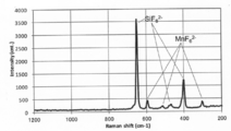
- FIG. 1 shows the Raman spectrum of the phosphor according to the embodiment and the assignment of its peak.
- the inventors of the present invention correspond to the Si—F bond appearing in the range of 650 ⁇ 10 cm ⁇ 1 of the peak detected in the Raman spectrum among the phosphors whose composition is represented by the formula (A).
- the ratio (I 1 / I 0) of the intensity of the peak corresponding to the Mn-F bond Raman shift appears in the range of 600 ⁇ 10cm -1 (I 1) is 0.09 or more 0
- a phosphor having a particle size of .22 or less has high external quantum efficiency and internal quantum efficiency. Specifically, in the phosphor according to the embodiment, the internal quantum efficiency is 80% or more.
- Non-Patent Document 1 peaks appearing in the range of Raman shift of 650 ⁇ 10 cm ⁇ 1 and 600 ⁇ 10 cm ⁇ 1 belong to the A1g mode, which is the stretching vibration of Si—F bond and Mn—F bond, respectively.
- A1g mode is the stretching vibration of Si—F bond and Mn—F bond, respectively.
- Non-Patent Document 1 the peak attributed to the Si—F bond appearing in the range of 480 ⁇ 10 cm ⁇ 1 and the peak attributed to the Mn—F bond appearing in the range of 520 ⁇ 10 cm ⁇ 1 both belong to the Eg mode. Both the peak attributed to the Si—F bond appearing in the range of 410 ⁇ 10 cm ⁇ 1 and the peak attributed to the Mn—F bond appearing in the range of 310 ⁇ 10 cm ⁇ 1 are both attributed to the F2g (T2g) mode. Yes.
- the total amount of Mn in the phosphor whose composition is represented by the formula (A) can be quantitatively determined by ICP emission spectroscopy, but is generally used for phosphors mainly composed of potassium silicofluoride.
- Such a synthesis method often contains Mn bonded to oxygen on the phosphor surface or the like, that is, MnO x, and it is difficult to detect only Mn related to light emission by ICP emission spectroscopy.
- the amount of Mn cannot be quantitatively determined in the Raman spectrum, but the Mn—F bond directly related to light emission can be determined as the intensity ratio of the Si—F bond.
- the external quantum efficiency ⁇ is a value calculated by multiplying the absorption rate ⁇ defined below and the internal quantum efficiency ⁇ ′.
- E ( ⁇ ) the entire spectrum of the excitation light source irradiated to the phosphor (photon number conversion)
- the external quantum efficiency ( ⁇ ) can be calculated by (I) ⁇ (II).
- External quantum efficiency, internal quantum efficiency, and absorption rate can be measured by, for example, a C9920-02G type absolute PL quantum yield measuring apparatus (trade name, manufactured by Hamamatsu Photonics Co., Ltd.).
- a C9920-02G type absolute PL quantum yield measuring apparatus (trade name, manufactured by Hamamatsu Photonics Co., Ltd.).
- blue light having a peak wavelength in the vicinity of 440 to 460 nm and a half width of 5 to 15 nm can be used.
- R A1g obtained from the Raman spectrum and the internal quantum efficiency and the relationship between R A1g and the external quantum efficiency are as shown in FIGS. 2 and 3 (details will be described later). It can be seen that the internal quantum efficiency and the external quantum efficiency are good when R A1g is in the range of 0.09 to 0.22.
- the phosphor according to the embodiment can be manufactured by an arbitrary method, and specifically, can be manufactured by the following method.
- an aqueous solution containing potassium permanganate and hydrogen fluoride is prepared as a reaction solution. And by making this reaction solution contact a silicon source, reaction advances on the surface of the silicon source, and fluorescent substance is formed.
- this reaction solution has a molar ratio of hydrogen fluoride to potassium permanganate (hereinafter referred to as “r H / K ”) of 87 or more (since there was a calculation error, the numerical value was corrected. ) Is 127 or less, preferably 90 or more and / or 120 or less.
- the concentration [HF] of hydrogen fluoride in the reaction solution is preferably 27% by mass or more and 40% by mass or less, and more preferably 28% by mass or more and 35% by mass or less.
- the phosphor according to an embodiment of the present invention has a crystal structure in which Mn is substituted for a part of the Si position in the K a SiF b matrix.
- the silicon source is oxidized by potassium permanganate and converted to silica, and the silica is fluorinated by HF.
- a K a SiF b matrix is produced by an ion exchange reaction.
- potassium permanganate becomes tetravalent Mn after oxidizing the silicon source, and is taken into the K a SiF b matrix.
- the reaction in which K a SiF b is produced from silica during this reaction process is very fast.
- the production reaction of tetravalent Mn is slower than the production rate of K a SiF b .
- the production rate of K a SiF b depends on the ratio of the proton [H + ] concentration to the [K + ] concentration in the reaction solution. That is, when the HF concentration increases, the dissolution rate of silica is accelerated, and the production reaction of K a SiF b is accelerated. On the other hand, since the valence change rate of Mn does not change, if the concentration of HF is too high, the amount of Mn taken into the K a SiF b matrix decreases. As a result, it is considered that the ratio of Mn—F bonds to Si—F bonds in the phosphor decreases.
- the concentration of HF contained in the reaction solution is high because the production of K a SiF b is promoted, an excessively high concentration reduces the [K +] concentration ratio in the reaction solution, so that the ion exchange reaction. It is considered that the yield of the phosphor is significantly reduced.
- a surface layer can also be formed on the surface of the phosphor particles thus produced by a coating process, for example, in order to improve moisture resistance and applicability during device fabrication.
- the material constituting the surface layer is selected from silicone resin, epoxy resin, fluororesin, tetraethoxysilane (TEOS), silica, zinc silicate, aluminum silicate, calcium polyphosphate, silicone oil, and silicone grease.
- TEOS tetraethoxysilane
- Zinc silicate and aluminum silicate are represented by, for example, ZnO ⁇ cSiO 2 (1 ⁇ c ⁇ 4) and Al 2 O 3 ⁇ dSiO 2 (1 ⁇ d ⁇ 10), respectively.
- the surface layer does not need to be completely covered with the phosphor particle surface, and a part of the particle surface may be exposed. If the surface layer made of the material as described above exists on a part of the surface of the phosphor particle, the effect can be obtained even if the entire surface is not completely covered.
- the surface layer is disposed by immersing phosphor particles in the dispersion or solution for a predetermined time and then drying by heating or the like. In order to obtain the effect of the surface layer without impairing the original function as the phosphor, the surface layer is preferably present in a volume ratio of 0.1 to 5% of the phosphor particles.
- the phosphor according to the embodiment can be classified according to the application method to the light emitting device to be used.
- the phosphor according to the embodiment of the present invention can be combined with a light emitting element having a light emission peak in the blue wavelength region to obtain the LED light emitting device according to the embodiment.
- the LED light emitting device according to the embodiment has higher emission intensity than the LED light emitting device using the conventional K 2 SiF 6 : Mn red phosphor.
- the phosphor according to the embodiment can be excited by an excitation light source having an emission peak in the ultraviolet to blue region.
- an excitation light source having an emission peak in the ultraviolet to blue region.
- a light emitting element having an emission peak in the wavelength region of 440 nm to 470 nm is used as an excitation light source. It is desirable to do. Use of a light emitting element having a light emission peak outside the above wavelength range is not preferable from the viewpoint of light emission efficiency.
- a solid light source element such as an LED chip or a laser diode can be used as the light emitting element.
- the phosphor according to the embodiment is a phosphor emitting red light. Therefore, a white light emitting device can be obtained by using in combination with a green light emitting phosphor and a yellow light emitting phosphor.
- the phosphor to be used can be arbitrarily selected according to the purpose of the light emitting device. For example, when a white light emitting device having a low color temperature is provided, a light emitting device having both efficiency and color rendering can be provided by combining the phosphor according to the embodiment and the yellow light emitting phosphor.
- the green light emitting phosphor and the yellow light emitting phosphor are phosphors having a main emission peak in a wavelength region of 520 nm or more and 570 nm or less.
- phosphors include silicate phosphors such as (Sr, Ca, Ba) 2 SiO 4 : Eu, Ca 3 (Sc, Mg) 2 Si 3 O 12 : Ce, (Y, Gd) 3 (Al, Ga) 5 O 12 : Ce, (Ca, Sr, Ba) Sulfide phosphors such as Ga 2 S 4 : Eu, (Ca, Sr, Ba) Si 2 O 2 N 2 : Eu, (Ca , Sr) - ⁇ SiAlON and the like alkaline earth oxynitride phosphors.
- the main emission peak is a wavelength at which the peak intensity of the emission spectrum is maximized, and the emission peak of the exemplified phosphor has been reported in the literature so far. Note that a change in emission peak of about 10 nm may be observed due to the addition of a small amount of elements or a slight compositional change during the preparation of the phosphor, and such a phosphor is also included in the phosphors exemplified above. Shall.
- a blue-green light emitting phosphor, an orange light emitting phosphor, and a red light emitting phosphor can be used depending on the application.
- silicate phosphors such as (Sr, Ca, Ba) 2 SiO 4 : Eu
- tungstate phosphors such as Li (Eu, Sm) W 2 O 8 , ( La, Gd, Y) 2 O 2 S: oxysulfide phosphors such as Eu, (Ca, Sr, Ba) S: sulfide phosphors such as Eu, (Sr, Ba, Ca) 2 Si 5 N 8 : Examples thereof include nitride phosphors such as Eu and (Sr, Ca) AlSiN 3 : Eu.
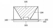
- FIG. 4 shows a cross section of a light emitting device according to an embodiment of the present invention.
- the light emitting device shown in the figure has a lead 100, a lead 101 and a stem 102, a semiconductor light emitting element 103, a reflecting surface 104, and a phosphor layer 105.
- a semiconductor light emitting element 103 is mounted with Ag paste or the like at the bottom center.
- the semiconductor light emitting element 103 an element that emits ultraviolet light or an element that emits light in the visible region can be used.
- semiconductor light emitting diodes such as GaAs and GaN.
- the arrangement of the lead 100 and the lead 101 can be changed as appropriate.
- the phosphor layer 105 is disposed in the recess of the light emitting device.
- the phosphor layer 105 can be formed by dispersing the phosphor according to the embodiment in a ratio of 5 wt% or more and 50 wt% or less in a resin layer 211 made of, for example, a silicone resin.
- the phosphor can be attached by various binders such as an organic material resin and an inorganic material glass.
- a transparent resin excellent in light resistance such as an epoxy resin and an acrylic resin is suitable in addition to the above-described silicone resin.
- Low-melting glass using alkaline earth borate or the like as a binder for inorganic materials, such as ultrafine silica, alumina, etc., for attaching phosphors with large particle diameter, alkaline earth phosphate obtained by precipitation method Salt etc. are suitable.
- These binders may be used alone or in combination of two or more.
- the phosphor used in the phosphor layer can be coated on the surface as necessary. This surface coating prevents the phosphor from being deteriorated by external factors such as heat, humidity, and ultraviolet rays. Further, the dispersibility of the phosphor can be adjusted, and the phosphor layer can be easily designed.
- an n-type substrate may be used for the semiconductor light emitting element 103 to have the following configuration. Specifically, an n-type electrode is formed on the back surface of the n-type substrate, a p-type electrode is formed on the upper surface of the semiconductor layer on the substrate, and the n-type electrode or the p-type electrode is mounted on a lead. The p-type electrode or the n-type electrode can be connected to the other lead by a wire.
- the size of the semiconductor light emitting element 103 and the dimensions and shape of the recesses can be changed as appropriate.
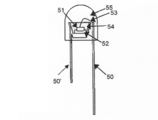
- FIG. 5 shows an example of a bullet-type light emitting device.
- the semiconductor light emitting element 51 is mounted on the lead 50 ′ via the mount material 52 and covered with the pre-dip material 54.
- a lead 50 is connected to the semiconductor light emitting element 51 by a wire 53 and is enclosed by a casting material 55.
- the pre-dip material 54 contains the phosphor according to the embodiment.
- the light emitting device according to the embodiment for example, the white LED is used not only for general illumination, but also as a light emitting device used in combination with a filter such as a color filter and the light emitting device, for example, a light source for a liquid crystal backlight. Is also optimal. Specifically, it can also be used as a red light emitting material for an inorganic electroluminescent device using a liquid crystal backlight source or a blue light emitting layer.
- Examples 1 to 3 A commercially available Si single crystal was prepared as a raw material. Further, 10.8 g of KMnO 4 powder, 250 ml of HF aqueous solution (49% by mass), and 150 ml of pure water were sufficiently mixed to obtain a reaction solution. The molar ratio of hydrogen fluoride to potassium permanganate in this reaction solution is 103, and the concentration of hydrogen fluoride [HF] is 31.5% by mass. Was allowed to react for 40 minutes. At this time, the reaction solution was stirred slowly to make the reaction solution uniform. As a result, a phosphor was formed on the surface of the Si single crystal, and the phosphor particles grown and enlarged were separated from the surface of the Si single crystal and deposited on the bottom of the container.
- the Raman spectrum of the obtained phosphor was measured, and R A1g was calculated. Furthermore, the internal quantum efficiency and the external quantum efficiency were measured with a C9920-02G type absolute PL quantum yield measuring apparatus (trade name, manufactured by Hamamatsu Photonics Co., Ltd.).
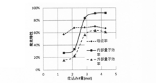
- the phosphors of Examples 2 and 3 and Comparative Examples 1 and 2 were prepared by changing the mixing ratio of the raw materials, and R A1g , internal quantum efficiency, and external quantum efficiency were similarly determined. The obtained results were as shown in Table 1 and FIGS.
- Examples 4 to 5 and Comparative Examples 3 to 7 Using KMnO 4 powder and an aqueous HF solution, the mixing ratio was changed to prepare reaction solutions shown in Table 2, and a phosphor was prepared in the same manner as in Example 1.
- Table 2 also shows the internal quantum efficiency, the external quantum efficiency, and the phosphor yield of the obtained phosphor.
- FIGS. 6 and 7 show the relationship between the absorption rate, the internal quantum efficiency, and the external quantum efficiency with respect to the [HF] concentration, and the phosphor yield with respect to the [HF] concentration.
- DESCRIPTION OF SYMBOLS 100 ... Lead; 101 ... Lead; 102 ... Stem; 103 ... Semiconductor light-emitting device; DESCRIPTION OF SYMBOLS 104 ... Reflecting surface; 105 ... Phosphor layer 50, 50 '... Lead; 51 ... Semiconductor light emitting element; 52 ... Mounting material 53 ... Bonding wire; 54 ... Pre-dip material;
Landscapes
- Chemical & Material Sciences (AREA)
- Inorganic Chemistry (AREA)
- Engineering & Computer Science (AREA)
- Materials Engineering (AREA)
- Organic Chemistry (AREA)
- Luminescent Compositions (AREA)
- Led Device Packages (AREA)
Priority Applications (4)
| Application Number | Priority Date | Filing Date | Title |
|---|---|---|---|
| KR1020167017423A KR20160092003A (ko) | 2013-12-09 | 2014-12-09 | 형광체, 그의 제조 방법, 및 상기 형광체를 사용한 발광 장치 |
| CN201480065679.0A CN105793388A (zh) | 2013-12-09 | 2014-12-09 | 荧光体及其制造方法、以及使用了该荧光体的发光装置 |
| KR1020177036905A KR101940439B1 (ko) | 2013-12-09 | 2014-12-09 | 형광체 및 그의 제조 방법, 및 상기 형광체를 포함하는 발광 장치 |
| US15/175,627 US10519368B2 (en) | 2013-12-09 | 2016-06-07 | Phosphor, manufacturing method thereof, and light-emitting device using the phosphor |
Applications Claiming Priority (2)
| Application Number | Priority Date | Filing Date | Title |
|---|---|---|---|
| JP2013254437A JP6342146B2 (ja) | 2013-12-09 | 2013-12-09 | 蛍光体、およびその製造方法、ならびにその蛍光体を用いた発光装置 |
| JP2013-254437 | 2013-12-09 |
Related Child Applications (1)
| Application Number | Title | Priority Date | Filing Date |
|---|---|---|---|
| US15/175,627 Continuation US10519368B2 (en) | 2013-12-09 | 2016-06-07 | Phosphor, manufacturing method thereof, and light-emitting device using the phosphor |
Publications (1)
| Publication Number | Publication Date |
|---|---|
| WO2015087861A1 true WO2015087861A1 (ja) | 2015-06-18 |
Family
ID=53371163
Family Applications (1)
| Application Number | Title | Priority Date | Filing Date |
|---|---|---|---|
| PCT/JP2014/082516 WO2015087861A1 (ja) | 2013-12-09 | 2014-12-09 | 蛍光体、およびその製造方法、ならびにその蛍光体を用いた発光装置 |
Country Status (6)
Cited By (1)
| Publication number | Priority date | Publication date | Assignee | Title |
|---|---|---|---|---|
| US9944848B2 (en) | 2014-09-30 | 2018-04-17 | Nichia Corporation | Fluoride fluorescent material, method for producing the same, and light emitting device |
Families Citing this family (9)
| Publication number | Priority date | Publication date | Assignee | Title |
|---|---|---|---|---|
| JP2016088950A (ja) * | 2014-10-30 | 2016-05-23 | 信越化学工業株式会社 | 赤色蛍光体 |
| CN105181671B (zh) * | 2015-09-21 | 2018-06-26 | 中国科学院长春光学精密机械与物理研究所 | 测试氮化物荧光粉老化程度的方法 |
| CN105331360A (zh) * | 2015-10-30 | 2016-02-17 | 烟台希尔德新材料有限公司 | Led红色荧光粉及其组合物的产业化制备方法以及产品和应用 |
| JP2018002813A (ja) | 2016-06-29 | 2018-01-11 | 株式会社東芝 | 蛍光体および発光装置 |
| US9929321B2 (en) | 2016-08-04 | 2018-03-27 | Kabushiki Kaisha Toshiba | Phosphor, producing method thereof and light-emitting device employing the phosphor |
| JP6812231B2 (ja) * | 2016-12-20 | 2021-01-13 | デンカ株式会社 | フッ化物蛍光体の製造方法 |
| JP2019044018A (ja) * | 2017-08-30 | 2019-03-22 | デンカ株式会社 | フッ化物蛍光体及び発光装置 |
| JP2019044017A (ja) * | 2017-08-30 | 2019-03-22 | デンカ株式会社 | フッ化物蛍光体及び発光装置 |
| US10608148B2 (en) * | 2018-05-31 | 2020-03-31 | Cree, Inc. | Stabilized fluoride phosphor for light emitting diode (LED) applications |
Citations (4)
| Publication number | Priority date | Publication date | Assignee | Title |
|---|---|---|---|---|
| WO2009119486A1 (ja) * | 2008-03-25 | 2009-10-01 | 国立大学法人群馬大学 | 蛍光体及びその製造方法並びに該蛍光体を用いた白色発光ダイオード |
| JP2010209311A (ja) * | 2008-09-05 | 2010-09-24 | Mitsubishi Chemicals Corp | 蛍光体及びその製造方法と、その蛍光体を用いた蛍光体含有組成物及び発光装置、並びに、その発光装置を用いた画像表示装置及び照明装置 |
| JP2013014715A (ja) * | 2011-07-06 | 2013-01-24 | Nichia Corp | フッ化物蛍光体及びそのフッ化物蛍光体を用いた発光装置 |
| WO2013137144A1 (ja) * | 2012-03-15 | 2013-09-19 | 株式会社 東芝 | 白色照明装置 |
Family Cites Families (7)
| Publication number | Priority date | Publication date | Assignee | Title |
|---|---|---|---|---|
| US7497973B2 (en) | 2005-02-02 | 2009-03-03 | Lumination Llc | Red line emitting phosphor materials for use in LED applications |
| KR101592836B1 (ko) | 2008-02-07 | 2016-02-05 | 미쓰비시 가가꾸 가부시키가이샤 | 반도체 발광 장치, 백라이트, 컬러 화상 표시 장치, 및 그들에 사용하는 형광체 |
| JP5105132B1 (ja) | 2011-06-02 | 2012-12-19 | 三菱化学株式会社 | 半導体発光装置、半導体発光システムおよび照明器具 |
| EP2663611B1 (en) * | 2011-12-16 | 2014-07-23 | Koninklijke Philips N.V. | Mn-activated hexafluorosilicates for led applications |
| JP2014177511A (ja) | 2013-03-13 | 2014-09-25 | Toshiba Corp | 蛍光体、およびその製造方法、ならびにその蛍光体を用いた発光装置 |
| JP2014177586A (ja) * | 2013-03-15 | 2014-09-25 | Toshiba Corp | 蛍光体、およびその製造方法、ならびにその蛍光体を用いた発光装置 |
| CN103540314B (zh) * | 2013-10-10 | 2015-01-14 | 上海师范大学 | 一种低温合成的氟硅酸盐纳米棒红色荧光粉及其制备方法 |
-
2013
- 2013-12-09 JP JP2013254437A patent/JP6342146B2/ja active Active
-
2014
- 2014-12-08 TW TW103142609A patent/TWI529978B/zh active
- 2014-12-09 CN CN202011484047.1A patent/CN112500855A/zh active Pending
- 2014-12-09 KR KR1020167017423A patent/KR20160092003A/ko not_active Ceased
- 2014-12-09 WO PCT/JP2014/082516 patent/WO2015087861A1/ja active Application Filing
- 2014-12-09 CN CN201480065679.0A patent/CN105793388A/zh active Pending
- 2014-12-09 KR KR1020177036905A patent/KR101940439B1/ko active Active
-
2016
- 2016-06-07 US US15/175,627 patent/US10519368B2/en active Active
Patent Citations (4)
| Publication number | Priority date | Publication date | Assignee | Title |
|---|---|---|---|---|
| WO2009119486A1 (ja) * | 2008-03-25 | 2009-10-01 | 国立大学法人群馬大学 | 蛍光体及びその製造方法並びに該蛍光体を用いた白色発光ダイオード |
| JP2010209311A (ja) * | 2008-09-05 | 2010-09-24 | Mitsubishi Chemicals Corp | 蛍光体及びその製造方法と、その蛍光体を用いた蛍光体含有組成物及び発光装置、並びに、その発光装置を用いた画像表示装置及び照明装置 |
| JP2013014715A (ja) * | 2011-07-06 | 2013-01-24 | Nichia Corp | フッ化物蛍光体及びそのフッ化物蛍光体を用いた発光装置 |
| WO2013137144A1 (ja) * | 2012-03-15 | 2013-09-19 | 株式会社 東芝 | 白色照明装置 |
Non-Patent Citations (1)
| Title |
|---|
| SADAO ADACHI ET AL.: "Direct synthesis and properties of K2SiF6:Mn4+ phosphor by wet chemical etching of Si wafer", JOURNAL OF APPLIED PHYSICS, vol. 104, 18 July 2008 (2008-07-18), pages 023512 * |
Cited By (2)
| Publication number | Priority date | Publication date | Assignee | Title |
|---|---|---|---|---|
| US9944848B2 (en) | 2014-09-30 | 2018-04-17 | Nichia Corporation | Fluoride fluorescent material, method for producing the same, and light emitting device |
| US10400166B2 (en) | 2014-09-30 | 2019-09-03 | Nichia Corporation | Fluoride fluorescent material and light emitting device |
Also Published As
| Publication number | Publication date |
|---|---|
| KR20180002893A (ko) | 2018-01-08 |
| KR101940439B1 (ko) | 2019-01-18 |
| US20160340577A1 (en) | 2016-11-24 |
| TWI529978B (zh) | 2016-04-11 |
| KR20160092003A (ko) | 2016-08-03 |
| TW201530830A (zh) | 2015-08-01 |
| CN112500855A (zh) | 2021-03-16 |
| US10519368B2 (en) | 2019-12-31 |
| JP2015113362A (ja) | 2015-06-22 |
| JP6342146B2 (ja) | 2018-06-13 |
| CN105793388A (zh) | 2016-07-20 |
Similar Documents
| Publication | Publication Date | Title |
|---|---|---|
| JP6342146B2 (ja) | 蛍光体、およびその製造方法、ならびにその蛍光体を用いた発光装置 | |
| JP5840540B2 (ja) | 白色照明装置 | |
| TWI650404B (zh) | 螢光體、及其製造方法以及使用該螢光體之發光裝置 | |
| JP6603458B2 (ja) | 蛍光体、およびその製造方法、ならびにその蛍光体を用いた発光装置 | |
| WO2014141851A1 (ja) | 蛍光体、およびその製造方法、ならびにその蛍光体を用いた発光装置 | |
| JP6486990B2 (ja) | 蛍光体、およびその製造方法、ならびにその蛍光体を用いた発光装置 | |
| JP5915801B1 (ja) | フッ化物蛍光体及びその製造方法並びに発光装置 | |
| WO2016136066A1 (ja) | フッ化物蛍光体複合体、およびその製造方法、ならびにその複合体を用いた発光装置 | |
| JP2018024870A (ja) | 蛍光体、及びその製造方法、並びにその蛍光体を用いた発光装置 | |
| JP6066003B2 (ja) | フッ化物蛍光体及びその製造方法並びに発光装置 | |
| TWI619799B (zh) | Phosphor, manufacturing method thereof, and illuminating device using the same | |
| US10032967B2 (en) | Phosphor and light-emitting device | |
| JP6344460B2 (ja) | フッ化物蛍光体の製造方法 | |
| JP2017052826A (ja) | 蛍光材料、およびその製造方法、ならびにその蛍光材料を用いた発光装置 |
Legal Events
| Date | Code | Title | Description |
|---|---|---|---|
| 121 | Ep: the epo has been informed by wipo that ep was designated in this application |
Ref document number: 14870458 Country of ref document: EP Kind code of ref document: A1 |
|
| NENP | Non-entry into the national phase |
Ref country code: DE |
|
| ENP | Entry into the national phase |
Ref document number: 20167017423 Country of ref document: KR Kind code of ref document: A |
|
| 122 | Ep: pct application non-entry in european phase |
Ref document number: 14870458 Country of ref document: EP Kind code of ref document: A1 |