WO2015083416A1 - 撮像装置及び内視鏡 - Google Patents
撮像装置及び内視鏡 Download PDFInfo
- Publication number
- WO2015083416A1 WO2015083416A1 PCT/JP2014/074547 JP2014074547W WO2015083416A1 WO 2015083416 A1 WO2015083416 A1 WO 2015083416A1 JP 2014074547 W JP2014074547 W JP 2014074547W WO 2015083416 A1 WO2015083416 A1 WO 2015083416A1
- Authority
- WO
- WIPO (PCT)
- Prior art keywords
- imaging device
- housing
- heat transfer
- transfer member
- main surface
- Prior art date
Links
Images


Classifications
-
- A—HUMAN NECESSITIES
- A61—MEDICAL OR VETERINARY SCIENCE; HYGIENE
- A61B—DIAGNOSIS; SURGERY; IDENTIFICATION
- A61B1/00—Instruments for performing medical examinations of the interior of cavities or tubes of the body by visual or photographical inspection, e.g. endoscopes; Illuminating arrangements therefor
- A61B1/04—Instruments for performing medical examinations of the interior of cavities or tubes of the body by visual or photographical inspection, e.g. endoscopes; Illuminating arrangements therefor combined with photographic or television appliances
- A61B1/05—Instruments for performing medical examinations of the interior of cavities or tubes of the body by visual or photographical inspection, e.g. endoscopes; Illuminating arrangements therefor combined with photographic or television appliances characterised by the image sensor, e.g. camera, being in the distal end portion
- A61B1/051—Details of CCD assembly
-
- A—HUMAN NECESSITIES
- A61—MEDICAL OR VETERINARY SCIENCE; HYGIENE
- A61B—DIAGNOSIS; SURGERY; IDENTIFICATION
- A61B1/00—Instruments for performing medical examinations of the interior of cavities or tubes of the body by visual or photographical inspection, e.g. endoscopes; Illuminating arrangements therefor
- A61B1/00064—Constructional details of the endoscope body
- A61B1/0011—Manufacturing of endoscope parts
-
- A—HUMAN NECESSITIES
- A61—MEDICAL OR VETERINARY SCIENCE; HYGIENE
- A61B—DIAGNOSIS; SURGERY; IDENTIFICATION
- A61B1/00—Instruments for performing medical examinations of the interior of cavities or tubes of the body by visual or photographical inspection, e.g. endoscopes; Illuminating arrangements therefor
- A61B1/00112—Connection or coupling means
- A61B1/00121—Connectors, fasteners and adapters, e.g. on the endoscope handle
- A61B1/00124—Connectors, fasteners and adapters, e.g. on the endoscope handle electrical, e.g. electrical plug-and-socket connection
-
- A—HUMAN NECESSITIES
- A61—MEDICAL OR VETERINARY SCIENCE; HYGIENE
- A61B—DIAGNOSIS; SURGERY; IDENTIFICATION
- A61B1/00—Instruments for performing medical examinations of the interior of cavities or tubes of the body by visual or photographical inspection, e.g. endoscopes; Illuminating arrangements therefor
- A61B1/005—Flexible endoscopes
-
- A—HUMAN NECESSITIES
- A61—MEDICAL OR VETERINARY SCIENCE; HYGIENE
- A61B—DIAGNOSIS; SURGERY; IDENTIFICATION
- A61B1/00—Instruments for performing medical examinations of the interior of cavities or tubes of the body by visual or photographical inspection, e.g. endoscopes; Illuminating arrangements therefor
- A61B1/12—Instruments for performing medical examinations of the interior of cavities or tubes of the body by visual or photographical inspection, e.g. endoscopes; Illuminating arrangements therefor with cooling or rinsing arrangements
- A61B1/128—Instruments for performing medical examinations of the interior of cavities or tubes of the body by visual or photographical inspection, e.g. endoscopes; Illuminating arrangements therefor with cooling or rinsing arrangements provided with means for regulating temperature
-
- G—PHYSICS
- G02—OPTICS
- G02B—OPTICAL ELEMENTS, SYSTEMS OR APPARATUS
- G02B23/00—Telescopes, e.g. binoculars; Periscopes; Instruments for viewing the inside of hollow bodies; Viewfinders; Optical aiming or sighting devices
- G02B23/24—Instruments or systems for viewing the inside of hollow bodies, e.g. fibrescopes
- G02B23/2476—Non-optical details, e.g. housings, mountings, supports
- G02B23/2492—Arrangements for use in a hostile environment, e.g. a very hot, cold or radioactive environment
-
- H—ELECTRICITY
- H04—ELECTRIC COMMUNICATION TECHNIQUE
- H04N—PICTORIAL COMMUNICATION, e.g. TELEVISION
- H04N23/00—Cameras or camera modules comprising electronic image sensors; Control thereof
- H04N23/50—Constructional details
- H04N23/52—Elements optimising image sensor operation, e.g. for electromagnetic interference [EMI] protection or temperature control by heat transfer or cooling elements
-
- H—ELECTRICITY
- H04—ELECTRIC COMMUNICATION TECHNIQUE
- H04N—PICTORIAL COMMUNICATION, e.g. TELEVISION
- H04N23/00—Cameras or camera modules comprising electronic image sensors; Control thereof
- H04N23/50—Constructional details
- H04N23/54—Mounting of pick-up tubes, electronic image sensors, deviation or focusing coils
-
- A—HUMAN NECESSITIES
- A61—MEDICAL OR VETERINARY SCIENCE; HYGIENE
- A61B—DIAGNOSIS; SURGERY; IDENTIFICATION
- A61B1/00—Instruments for performing medical examinations of the interior of cavities or tubes of the body by visual or photographical inspection, e.g. endoscopes; Illuminating arrangements therefor
- A61B1/00163—Optical arrangements
-
- H—ELECTRICITY
- H04—ELECTRIC COMMUNICATION TECHNIQUE
- H04N—PICTORIAL COMMUNICATION, e.g. TELEVISION
- H04N23/00—Cameras or camera modules comprising electronic image sensors; Control thereof
- H04N23/50—Constructional details
- H04N23/555—Constructional details for picking-up images in sites, inaccessible due to their dimensions or hazardous conditions, e.g. endoscopes or borescopes
Definitions
- the present invention relates to an imaging device in which an imaging device and a heat transfer member joined to the imaging device are housed in a housing, and an endoscope having the imaging device.
- the imaging element which consists of a semiconductor in which the light-receiving part was formed in the main surface is small, it is used for an electronic endoscope etc. However, when the temperature of the imaging device rises during operation, the imaging device may be degraded or the image quality may be deteriorated due to thermal noise.
- the imaging device which suppresses the temperature rise of an imaging device is reported by heat-transferring the heat
- one end of a flexible substrate is connected to a CCD (imaging element), and the other end of the flexible substrate is on the inner wall surface of a protective frame made of metal having high thermal conductivity.
- An electronic endoscope having an imaging device in close proximity is disclosed.
- the protective frame has a spring portion and reliably contacts the inner circumferential surface of the cylindrical portion. As a result, the heat generated from the CCD is dissipated to the protective frame.
- An object of the present invention is to provide an imaging device that efficiently dissipates heat generated by an imaging device, and an endoscope having the imaging device.
- An imaging device includes an imaging element having a first main surface and a second main surface, and a light receiving unit formed on the first main surface, and an external connection of the imaging element.
- a wiring board having a device electrode pad connected to a terminal, a wire connected to the device electrode pad and one end, and a bonding portion bonded to the second main surface of the imaging device;
- a heat transfer member made of a material having a thermal conductivity of 15 W / (m ⁇ K) or more, including a bent portion extended from the joint portion and a fixed portion extended from the bent portion;
- a housing made of metal is in contact with a part of the fixed part of the heat transfer member accommodated and the inner surface.
- an endoscope includes an imaging device having a first main surface and a second main surface, and a light receiving unit formed on the first main surface, A wiring board having an element electrode pad connected to the external connection terminal of the imaging element, and a wire connected to the element electrode pad and one end, and joined to the second main surface of the imaging element Heat transfer comprising a material having a thermal conductivity of 15 W / (m ⁇ K) or more, including a bonding portion, a bending portion extending from the bonding portion, and a fixing portion extending from the bending portion It has an imaging device which comprises a member, and a case which consists of metal which a part of said fixed parts of said heat transfer member stored inside and the inner surface contact.
- an imaging device that efficiently dissipates heat generated by an imaging device, and an endoscope having the imaging device.
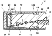
- the imaging device 1 according to the present embodiment is, for example, small in diameter and ultra-compact because the imaging device 1 is disposed at the tip of the electronic endoscope.
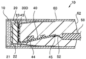
- the imaging device 1 includes a cover glass 10, an imaging element 20, a heat transfer member 30, a wiring board 40, a cable 50, and a housing 60.
- An imaging unit including the cover glass 10, the imaging element 20, the heat transfer member 30, and the wiring board 40 is housed inside the housing 60.
- the inside of the case 60 is filled with the resin 62, but it is not shown in FIG. 1 etc.
- the imaging element 20 exchanges electrical signals with a processor (not shown) connected to the cable 50 via the wiring board 40. That is, the plurality of external connection terminals 23 of the imaging element 20 are joined to the respective element electrode pads 42 (hereinafter referred to as “electrode pads 42") of one end of the wiring 43 of the wiring board 40 on which the electronic component 44 is mounted. There is.
- the plurality of cable electrode pads 45 (hereinafter referred to as “electrode pads 45”) at the other end of the wiring 43 are each connected to the conducting wire 52 of the signal cable 50.
- the imaging device 1 has a heat transfer member 30.
- the heat transfer member 30 is partially joined to the imaging device 20, and transfers heat generated by the imaging device 20 to the housing 60 in contact with the other portion.
- the imaging element 20 is a substantially rectangular chip in which the light receiving unit 21 formed of a solid-state imaging circuit is formed on the first main surface 20SA.
- the solid-state imaging circuit is formed of a CCD, a CMOS sensor or the like.
- the imaging device 20 may be a backside illumination type.
- An external connection terminal 23 for exchanging signals with the light receiving unit 21 is formed on the second main surface 20SB via the through wiring 22. That is, the plurality of external connection terminals 23 are arranged in an array on the second main surface 20SB.
- the first main surface 20SA has a wiring from the light receiving unit 21 to the through wiring 22, and the second main surface 20SB has a wiring from the through wiring 22 to the external connection terminal 23, but Absent.
- the cover glass 10 is bonded to the first main surface 20SA of the imaging device 20 via an adhesive layer (not shown). As will be described later, in the imaging device 1, the transparent wafer is bonded to a semiconductor wafer on which a plurality of light receiving portions and the like are formed, and then separated into pieces by dicing. It is the same as the planar view size of. Although the cover glass 10 has a protection function of the light receiving unit 21, it is not an essential component of the imaging device 1.
- the wiring board 40 is a flexible wiring board which uses a flexible resin such as polyimide as a base material and has a wiring 43 made of copper or the like.
- the wiring board 40 may be a single layer wiring board, or may be a multilayer wiring board in which wiring layers are formed on at least both surfaces.
- An electrode pad 42 is formed on the front end side of the wiring board 40, and an electrode pad 45 (see FIG. 2) is formed on the rear end side. The electrode pad 42 and the electrode pad 45 are electrically connected by the wiring 43.
- a connection pad (not shown) is formed on the wiring 43 of the wiring board 40, and an electronic component 44 such as a chip capacitor is mounted. That is, the wiring 43 constitutes an electronic circuit that processes a signal input from the imaging device 20 and outputs the processed signal to the signal cable 50.
- the wiring board 40 is bent halfway and is accommodated within the projection plane of the main surface of the imaging device 20.
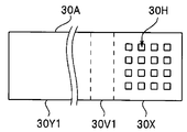
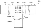
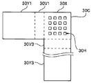
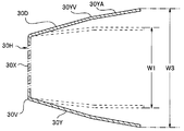
- the heat transfer member 30 includes a joint 30X joined to the second main surface 20SB of the imaging device 20, bent portions 30V1 and 30V2 extended from the joint 30X, and bent portions 30V1 and 30V2 respectively. And fixed portions 30Y1 and 30Y2 extended from the above.
- the last digit of the code may be omitted.
- each of the bending portions 30V1 and 30V2 is referred to as a bending portion 30V.
- the fixing portion 30Y is pressed against the inner surface of the housing 60 by the biasing force, and reliably abuts against the inner surface of the metal housing 60. . That is, the bending portion 30V, which is a spring, presses the fixing portion 30Y to the inner surface of the housing 60.
- the heat generated by the imaging element 20 is transferred to the housing 60 through the heat transfer member 30 having high thermal conductivity, so that the heat is efficiently dissipated. Therefore, the temperature of the image pickup device 20 does not excessively rise at the time of operation, so that the image pickup device 20 is not deteriorated or the image quality is not deteriorated by the thermal noise.
- the external connection terminal 23 is provided on the second main surface 20SB of the imaging element 20, the position facing the external connection terminal 23 of the heat transfer member 30, in other words, the electrode pad 42 of the wiring board 40 There is a through hole 30H at the opposite position.
- the plan view shape of the joint portion 30X of the heat transfer member 30 is substantially rectangular like the imaging device 20, and the bent portion 30V and the fixing portion 30Y are opposed among the four sides of the joint portion 30X. It extends from two sides. That is, although the heat transfer member 30 includes the plurality of extended bending portions 30V and the plurality of fixing portions 30Y, these are integrated, and the boundaries thereof are not clearly distinguishable.
- the heat transfer member 30 is a thin plate made of an elastic metal material having high thermal conductivity such as stainless steel, copper, phosphor bronze, copper alloy and the like. Then, as shown in FIG. 3, the bending portion 30 ⁇ / b> V is bent and plastically deformed before being accommodated inside the housing 60.
- the length of the end of the fixing portion 30Y1 of the heat transfer member 30 in which the bent portion 30V is plastically deformed and the end of the fixing portion 30Y2 is illustrated as W3.
- the length W3 is longer than the inner dimension W1 of the housing 60.
- the fixing portion 30Y when the fixing portion 30Y is housed inside the housing 60, the fixing portion 30Y is pressed against the inner surface of the housing 60 by the biasing force, and reliably abuts on the housing 60.
- the housing 60 may use a material having a high thermal conductivity ⁇ , for example, the same material as the material of the heat transfer member 30. However, as a material of the heat transfer member 30, it is preferable to use a material having a thermal conductivity ⁇ higher than that of the housing 60. For example, it is particularly preferable to configure the case 60 with stainless steel and the heat transfer member 30 with copper.
- the adhesive agent which consists of resin with high heat conductivity.
- the thermal conductivity of the bonding member is preferably 1 W / (m ⁇ K) or more, and particularly preferably 15 W / (m ⁇ K) or more.
- a plurality of imaging devices 20 each having a light receiving unit 21 are formed on a silicon substrate using a known semiconductor process. Then, after adhering to the formation surface of the light receiving unit 21 with a glass wafer of substantially the same size as the silicon substrate as a protective material, grinding is performed from the back surface side of the silicon substrate. After the thickness of the silicon substrate is reduced by grinding, through holes are formed from the back surface side by etching or the like. An insulating film is formed on the side wall of the formed through hole, and the inside is made conductive by a conductive paste, a plating method, a sputtering method or the like, whereby the through wiring 22 is formed. Thereafter, the silicon substrate to which the glass wafer is bonded is cut into pieces, whereby the imaging device 20 to which the cover glass 10 is bonded is manufactured.
- electrode pads 42, 45 and wiring 43 are manufactured by bonding and etching a copper foil and a polyimide as a base material or using a plating method or the like, and an electronic component 44 is mounted.
- the heat transfer member 30 is produced, for example, by pressing or etching a copper plate.
- local heat treatment or the like may be applied to only the bending portion 30V by laser irradiation or the like. Then, the bent portion 30V is bent and plastically deformed so that the length between the end of the fixed portion 30Y1 and the end of the fixed portion 30Y2 is W3.
- the length W3 may be larger than the inner size W1 of the housing 60, but it is 110% or more and 200% or less of W1 in consideration of the balance between the ease of insertion into the housing and the strength of the biasing force. Is preferred.
- a shape memory alloy such as a titanium nickel alloy may be used as the material of the heat transfer member 30. That is, after bending bent portion 30V of heat transfer member 30 storing the state in which bent portion 30V is deformed and fixing portion 30Y is largely opened, heat is applied to a predetermined temperature after housing fixed portion 30Y. The inner surface of the case 60 can be pressed by the biasing force.
- the bonding portion 30X of the heat transfer member 30 is bonded to the second main surface 20SB of the imaging element 20 by a bonding member. At this time, bonding is performed so that the external connection terminal 23 of the imaging element 20 is positioned inside the through hole 30H of the heat transfer member 30.
- the periphery of the bonding portion 30X may be resin-sealed so that the resin is injected into the through hole 30H.
- an imaging unit in which the cover glass 10, the imaging element 20, the heat transfer member 30, the wiring board 40, and the signal cable 50 are integrated is inserted into the inside of the housing 60.
- the plan view shape and the inner size of the housing 60 are substantially the same and slightly larger than the plan view shape and the outer size of the imaging device 20.
- the inner dimension W1 in the vertical direction of the housing 60 shown in FIG. 3 is substantially the same as the outer dimension W2 in the vertical direction of the imaging device 20.
- the inside of the housing 60 is filled with the resin 62 to complete the imaging device 1.
- the heat transfer member 30 is in contact with the metal case 60 while being pressed.
- the heat transfer member 30 is deformed by being pressed against the inner surface of the housing 60 by adjusting the thickness, size, shape, etc., using an elastic body as the material, and makes the surface contact with the housing 60 be able to.
- the surface contact makes it possible to transfer the heat generated by the imaging device 20 to the housing 60 more efficiently.
- the imaging device 1 can efficiently dissipate the heat generated by the imaging element 20.
- the heat transfer member 30 and the wiring board 40 are housed in a casing of the same inner size as the outer size of the imaging device 20, the diameter is small.
- the bending portions 30V1 and 30V2 and the fixing portions 30Y1 and 30Y2 extend from the two opposing sides of the bonding portion 30X.
- the bent portion 30V1 and the fixing portion 30Y1 extend from one side of the joint portion 30X.
- bent portions 30V1, 30V2, 30V3 and fixed portions 30Y1, 30Y2, 30Y3 extend from three sides of the joint portion 30X.
- the bent portions 30V1 and 30V3 and the fixing portions 30Y1 and 30Y3 extend from two orthogonal sides of the bonding portion 30X.
- the imaging devices of Modifications 1 to 3 including the heat transfer members 30A, 30B, and 30C also have the same effect as the imaging device 1 of the first embodiment.
- the shape of the heat transfer member is selected according to the arrangement of the wiring board 40, the electronic component 44, and the signal cable 50 disposed inside the housing 60, the amount of heat generation of the imaging device, that is, the amount of heat to be dissipated. Ru.
- an imaging device 1D according to a second embodiment will be described. Since the imaging device 1D is similar to the imaging device 1 and the like, the same components will be denoted by the same reference numerals and descriptions thereof will be omitted.
- the heat transfer member 30D of the imaging device 1D has a bending portion 30YV in the fixing portion 30Y.
- the bent portion 30YV is plastically deformed in advance so that the tip end portion 30YA of the fixed portion 30Y is parallel to the inner surface of the housing 60 when the heat transfer member 30D is accommodated in the housing 60. Therefore, the front end portion 30YA is in surface contact with the inner surface of the housing 60 on the entire surface.
- the imaging device 1D has the same effect as the imaging device 1 and the contact area between the heat transfer member 30D and the housing 60 is wide, the heat generated by the imaging element 20 can be dissipated more efficiently.
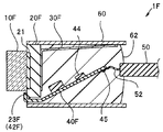
- an imaging device 1E according to a third embodiment will be described. Since the imaging device 1E is similar to the imaging device 1 and the like, the same components will be denoted by the same reference numerals and descriptions thereof will be omitted.
- a positioning portion 63 defining the position of the fixing portion 30Y in the inside of the housing 60E in the longitudinal direction, that is, the position of the imaging unit in the longitudinal direction It is arranged.
- the imaging unit in which the cover glass 10, the imaging element 20, the heat transfer member 30, the wiring board 40, and the signal cable 50 are integrated is inserted into the housing 60E from the front end side.
- the positioning position of the imaging unit in the longitudinal direction is defined by the positioning unit 63.
- the positioning portion 63 may be formed by arranging another member, or may be formed by processing a part of the housing 60E. In addition, a projection may be provided so that a part of the fixing portion 30Y is processed to be locked or engaged with the positioning portion 63.
- the imaging device 1E has effects of the imaging device 1 and the like, and can easily ensure the accuracy of the arrangement position of the imaging unit, for example, the imaging element 20.
- an elongated hole 60FH is formed in the contact surface of the heat transfer member 30F of the housing 60F. And, a part of the fixing portion 30Y of the heat transfer member 30F is processed into the convex portion 30FH so as to be fitted to the hole 60FH. That is, the hole 60FH of the housing 60F is a positioning portion having the function of a positioning member that defines the position of the fixing portion.
- heat transfer member 30F and housing 60F are fitted, material having high heat conductivity such as high thermal conductivity resin, solder, or Ag paste is injected into hole 60FH, and housing 60F and heat transfer member 30F The portion in contact may be fixed and sealed.
- material having high heat conductivity such as high thermal conductivity resin, solder, or Ag paste is injected into hole 60FH, and housing 60F and heat transfer member 30F The portion in contact may be fixed and sealed.
- the imaging device 1F of the modification has the effect of the imaging device 1E, and the hole 60H of the housing 60 and the convex portion 30FH of the fixed portion 30Y are fitted, so the contact area is large. Moreover, when the contact part of the housing
- an imaging device 1G according to a fourth embodiment will be described. Since the imaging device 1G is similar to the imaging device 1 and the like, the same components are denoted by the same reference numerals and descriptions thereof will be omitted.
- the external connection terminal 23G is disposed on the first main surface 20SA.
- the wiring board 40G is connected at one end to the external connection terminal 23G of the first main surface 20SA of the imaging element 20C, and the other end is disposed on the rear end side via the bent portion.
- the imaging device 1G has effects of the imaging device 1 and the like. Furthermore, the imaging device 20C without the through wiring is easy to manufacture. Moreover, there is no through hole 30H in the joint portion 30XG of the heat transfer member 30G. Therefore, the heat transfer member 30G can be easily manufactured. Furthermore, since the contact area between the imaging device 20G and the heat transfer member 30G is large, the heat generated by the imaging device 20 can be dissipated more efficiently.
- the endoscope 9 is an electronic endoscope having the imaging device 1 of the first embodiment at the distal end portion 2 of the insertion portion 3.
- the endoscope 9 includes an operation unit 4 disposed on the proximal end side of the insertion unit 3 and a universal cord 5 extending from the operation unit 4.
- the operation unit 4 is provided with various switches and the like operated by the operator while holding.
- the cable 50 of the imaging device 1 is connected to a main unit (not shown) that performs image processing and the like through the insertion portion 3 and the universal cord 5 and through the connector 6 disposed at the proximal end of the universal cord 5 Be done.
- the endoscope 9 having the imaging device 1 at its tip is minimally invasive. Then, in the endoscope 9, there is no possibility that the imaging device 1 is deteriorated due to an excessive temperature rise, or the image quality is not deteriorated due to the thermal noise.
- imaging device 2 endoscope 10: cover glass 20: imaging device 21: light receiving portion 30: heat transfer member 30V: bending portion 30X: bonding portion 30Y: fixing portion 42: element electrode pad 43: wiring 44: Electronic component 45: Cable electrode pad 50: Cable 60: Case
Abstract
【課題】、撮像素子20が発生した熱を効率的に放熱する撮像装置1を提供する。 【解決手段】撮像装置1は、受光部21が形成されている撮像素子20と、配線板40と、撮像素子20に接合されている接合部30Xと、接合部30Xから延設された屈曲部30Vと、屈曲部30Vから延設された固定部30Yとを含む、熱伝導率が、15W/(m・K)以上の材料からなる伝熱部材30と、内部に収容された伝熱部材30の固定部30Yの一部と内面が当接している金属からなる筐体60と、を具備する
Description
本発明は、撮像素子と前記撮像素子と接合された伝熱部材とが筐体内に収容されている撮像装置、及び、前記撮像装置を有する内視鏡に関する。
受光部が主面に形成された半導体からなる撮像素子は小型であるため、電子内視鏡等に使用されている。しかし、撮像素子の温度が作動時に上昇することで、撮像素子が劣化したり、熱ノイズにより画像品質が悪化したりすることがある。
このため、撮像素子が発生する熱を熱伝導性の高い部材で伝熱することで、撮像素子の温度上昇を抑制する撮像装置が報告されている。
例えば、日本国特開2011-200338号公報には、CCD(撮像素子)にフレキシブル基板の一端部が接続され、フレキシブル基板の他端が、熱伝導性が高い金属からなる保護枠の内壁面に密接されている撮像装置を有する電子内視鏡が開示されている。保護枠はバネ部を有し円筒部の内周面に確実に接触する。これによりCCDから発生した熱が保護枠に放熱される。
しかし、上記撮像装置では、撮像素子から保護枠への伝熱経路の途中に、熱伝導率の低い樹脂からなるフレキシブル基板を介している。このため、撮像素子が発生した熱が、保護枠へ十分には伝熱されないおそれがあった。
本発明は、撮像素子が発生した熱を効率的に放熱する撮像装置、及び、前記撮像装置を有する内視鏡を提供することを目的とする。
本発明の実施形態の撮像装置は、第1の主面と第2の主面とを有し、前記第1の主面に受光部が形成されている撮像素子と、前記撮像素子の外部接続端子と接続されている素子電極パッドと、前記素子電極パッドと一端が接続されている配線と、を有する配線板と、前記撮像素子の前記第2の主面に接合されている接合部と、前記接合部から延設された屈曲部と、前記屈曲部から延設された固定部とを含む、熱伝導率が、15W/(m・K)以上の材料からなる伝熱部材と、内部に収容された前記伝熱部材の前記固定部の一部と内面が当接している金属からなる筐体と、を具備する。
また、本発明の別の実施形態の内視鏡は、第1の主面と第2の主面とを有し、前記第1の主面に受光部が形成されている撮像素子と、前記撮像素子の外部接続端子と接続されている素子電極パッドと、前記素子電極パッドと一端が接続されている配線と、を有する配線板と、前記撮像素子の前記第2の主面に接合されている接合部と、前記接合部から延設された屈曲部と、前記屈曲部から延設された固定部とを含む、熱伝導率が、15W/(m・K)以上の材料からなる伝熱部材と、内部に収容された前記伝熱部材の前記固定部の一部と内面が当接している金属からなる筐体と、を具備する撮像装置を有する。
本発明の実施形態によれば、撮像素子が発生した熱を効率的に放熱する撮像装置、及び、前記撮像装置を有する内視鏡を提供できる。
<第1実施形態>
本実施の形態の撮像装置1は、例えば電子内視鏡の先端部に配設されるため細径で超小型である。
本実施の形態の撮像装置1は、例えば電子内視鏡の先端部に配設されるため細径で超小型である。
図1、図2、図3に示すように、撮像装置1は、カバーガラス10と、撮像素子20と、伝熱部材30と、配線板40と、ケーブル50と、筐体60と、を具備する。カバーガラス10と、撮像素子20と、伝熱部材30と、配線板40とを含む撮像ユニットは、筐体60の内部に収容されている。なお、図2等に示すように、筐体60の内部には樹脂62が充填されているが、図1等では図示していない。
撮像素子20は、配線板40を介してケーブル50と接続されているプロセッサ(不図示)と電気信号のやりとりをする。すなわち、撮像素子20の複数の外部接続端子23は、電子部品44が実装されている配線板40の配線43の一端のそれぞれの素子電極パッド42(以下「電極パッド42」という)と接合されている。配線43の他端の複数のケーブル電極用パッド45(以下「電極パッド45」という)は、それぞれが信号ケーブル50の導線52と接続されている。
そして、撮像装置1は伝熱部材30を有する。伝熱部材30は、一部が撮像素子20と接合されており、他の一部が当接している筐体60に撮像素子20が発生した熱を伝熱する。
以下、撮像装置1の構成要素について説明する。
撮像素子20は、第1の主面20SAに固体撮像回路からなる受光部21が形成されている略直方体のチップである。なお、固体撮像回路は、CCD、CMOSセンサ等からなる。撮像素子20は裏面照射型であってもよい。
受光部21と信号のやりとりをするための外部接続端子23は貫通配線22を介して第2の主面20SBに形成されている。すなわち複数の外部接続端子23はアレイ状に第2の主面20SBに配置されている。なお、第1の主面20SAには、受光部21から貫通配線22までの配線があり、第2の主面20SBには貫通配線22から外部接続端子23までの配線があるが、図示していない。
カバーガラス10は、撮像素子20の第1の主面20SAに接着層(不図示)を介して接着されている。後述するように、撮像装置1では、複数の受光部等が形成された半導体ウエハに透明ウエハを接着後に、ダイシングにより個片化されているため、撮像素子20の平面視寸法と、カバーガラス10の平面視寸法とは同じである。なお、カバーガラス10は受光部21の保護機能を有するが、撮像装置1の必須の構成要素ではない。
配線板40は、ポリイミド等の可撓性樹脂を基材とし、銅等からなる配線43を有するフレキシブル配線板である。配線板40は、単層配線板でもよいし、少なくとも両面に配線層が形成されている多層配線板であってもよい。配線板40の先端側には電極パッド42が、後端側には電極パッド45(図2参照)が形成されており、電極パッド42と電極パッド45とは配線43により電気的に接続されている。配線板40の配線43には接続パッド(不図示)が形成されており、チップコンデンサ等の電子部品44が実装されている。すなわち、配線43は撮像素子20から入力した信号を処理して信号ケーブル50に出力する電子回路を構成している。
なお、図1~図3等に示すように、配線板40は、途中で折り曲げられて、撮像素子20の主面の投影面内に納められている。
そして、伝熱部材30は、撮像素子20の第2の主面20SBに接合されている接合部30Xと、接合部30Xから延設された屈曲部30V1、30V2と、それぞれの屈曲部30V1、30V2から延設された固定部30Y1、30Y2とを含む。なお、以下、同じ機能の複数の構成要素をいうときには、その符号の最後の数字1文字を省略することがある。例えば、屈曲部30V1、30V2のそれぞれを、屈曲部30Vという。
伝熱部材30が筐体60の内部に収容されると、固定部30Yは、付勢力により筐体60の内面に押圧されている状態となり、確実に金属からなる筐体60の内面と当接する。すなわち、バネである屈曲部30Vは固定部30Yを筐体60の内面に押圧する。
撮像素子20が発生した熱は、熱伝導率が高い伝熱部材30を介して筐体60に伝熱されるので、効率的に放熱される。そのため、撮像素子20は、作動時に温度が過度に上昇することがないため、劣化したり、また熱ノイズにより画像品質が悪化したりすることがない。
なお、撮像装置1では、撮像素子20の第2の主面20SBに外部接続端子23があるため、伝熱部材30の外部接続端子23と対向する位置、言い換えれば、配線板40の電極パッド42と対向する位置に貫通孔30Hがある。
図4に示すように伝熱部材30の接合部30Xの平面視形状は、撮像素子20と同じように略矩形であり、屈曲部30V及び固定部30Yは接合部30Xの4辺のうち対向する2辺から延出している。すなわち、伝熱部材30は、延設された複数の屈曲部30V及び複数の固定部30Yを含むが、これらは一体であり、その境界は明瞭に区別できるものではない。
伝熱部材30は、ステンレス、銅、りん青銅、銅合金等の熱伝導率が高く、弾性のある金属材料からなる薄板である。そして、図3に示すように、屈曲部30Vは筐体60の内部に収容される前に、曲げられて塑性変形している。
図3では、屈曲部30Vが塑性変形した伝熱部材30の固定部30Y1の端部と固定部30Y2の端部との長さをW3として図示している。そして、長さW3は、筐体60の内寸W1よりも長い。
このため、筐体60の内部に収容されると、固定部30Yは、付勢力により筐体60の内面に押圧されている状態となり、確実に筐体60と当接する。
伝熱部材30の材料は、熱伝導率λが15W/(m・K)以上である。すなわち、伝熱部材30としては、例えば、銅(λ=398W/(m・K))、アルミニウム(λ=237W/(m・K))鉄(λ=84W/(m・K))、リン青銅(λ=60W/(m・K))、又は、ステンレス(λ=17W/(m・K))等を用いる。
筐体60には、熱伝導率λが高い材料、例えば伝熱部材30の材料と同じ材料を用いてもよい。しかし、伝熱部材30の材料には、筐体60よりも熱伝導率λが高い材料を用いることが好ましい。例えば、筐体60をステンレスで、伝熱部材30を銅で構成することが特に好ましい。
なお、伝熱部材30と撮像素子20とを接合する接合部材には、熱伝導率が高い樹脂からなる接着剤を用いることが好ましい。接合部材の熱伝導率は、1W/(m・K)以上が好ましく、15W/(m・K)以上であることが特に好ましい。
また、接合部材として、半田等の低融点金属を用いても良い。樹脂に比べてより熱伝導率の高い金属により接合することで、より効率的に伝熱できる。金属材料等の導電性材料を接合に用いた場合には、電気接続部との接触を防止する必要があることは言うまでも無い。
次に、撮像装置1の製造方法について説明する。
最初に、シリコン基板に公知の半導体プロセスを用いて受光部21を有する撮像素子20が複数形成される。そしてシリコン基板と略同サイズのガラスウエハを保護材として受光部21の形成面に接着後、シリコン基板の裏面側から研削加工が行われる。研削加工によりシリコン基板の厚さを薄くした後、裏面側からエッチング等により貫通孔を形成する。形成した貫通孔の側壁に絶縁膜を成膜し、内部を導電性ペーストやめっき法やスパッタ法等により導電化することで貫通配線22が形成される。その後、ガラスウエハが接着されたシリコン基板を切断により個片化することにより、カバーガラス10が接着された撮像素子20が作製される。
配線板40は銅箔と基材であるポリイミド等とを貼り合わせエッチングしたり、めっき法等を用いたりして電極パッド42、45、配線43が作製され、電子部品44が実装される。
伝熱部材30は、例えば、銅板をプレス加工したり、エッチング加工したりして作製される。屈曲部30Vの折り曲げ加工を容易にするように、屈曲部30Vだけにレーザー照射等により局所的熱処理等が施されていても良い。そして、固定部30Y1の端部と固定部30Y2の端部との長さがW3となるように、屈曲部30Vを折り曲げ加工し塑性変形する。
長さW3は、筐体60の内寸のW1よりも大きければ良いが、筐体内への挿入の容易さと、付勢力の強さとのバランスを考慮すると、W1の110%以上200%以下であることが好ましい。
なお、伝熱部材30の材料にチタンニッケル合金等の形状記憶合金を用いてもよい。すなわち、屈曲部30Vが変形し固定部30Yが大きく開いた状態を記憶した伝熱部材30の屈曲部30Vを折り曲げてから筐体内に収容した後に、所定温度に加熱することで、固定部30Yを付勢力により筐体60の内面に押圧できる。
撮像素子20の第2の主面20SBに、伝熱部材30の接合部30Xが接合部材により接合される。このとき、伝熱部材30の貫通孔30Hの内部に、撮像素子20の外部接続端子23が位置するように接合される。
次に、ケーブル50が接続された配線板40の電極パッド42と撮像素子20の外部接続端子23とが接合される。貫通孔30H内に樹脂が注入されるように、接合部30Xの周囲を樹脂封止してもよい。
そして、カバーガラス10と撮像素子20と伝熱部材30と配線板40と信号ケーブル50とが一体化した撮像ユニットが、筐体60の内部に挿入される。筐体60の平面視形状及び内寸は、撮像素子20の平面視形状及び外寸よりも略同じで僅かに大きい。例えば、図3に示す筐体60の縦方向の内寸W1は、撮像素子20の縦方向の外寸W2と略同じである。
そして、筐体60の内部に樹脂62が充填されることにより撮像装置1が完成する。
すでに説明したように、伝熱部材30は、金属からなる筐体60に押圧された状態で当接している。なお、伝熱部材30は、その材質として弾性体を用い、厚さ・寸法や形状等を調整することによって、筐体60の内面に押圧されることで変形し、筐体60と面接触させることができる。面接触させることで、撮像素子20で発生した熱をより効率的に筐体60へ伝熱させることが可能になる。
撮像装置1は、撮像素子20が発生した熱を効率的に放熱できる。また、伝熱部材30及び配線板40が撮像素子20の外寸と同じ内寸の筐体に収容されているため細径である。
<第1実施形態の変形例>
図4に示したように、撮像装置1の伝熱部材30は、接合部30Xの対向する2辺から、それぞれ屈曲部30V1、30V2、及び固定部30Y1、30Y2が延設していた。
図4に示したように、撮像装置1の伝熱部材30は、接合部30Xの対向する2辺から、それぞれ屈曲部30V1、30V2、及び固定部30Y1、30Y2が延設していた。
これに対して、図5に示す変形例1の伝熱部材30Aは接合部30Xの1辺から、屈曲部30V1及び固定部30Y1が延設している。
また、図6に示す変形例2の伝熱部材30Bは接合部30Xの3辺から、屈曲部30V1、30V2、30V3及び固定部30Y1、30Y2、30Y3が延設している。
また、図7に示す変形例3の伝熱部材30Cは接合部30Xの直交する2辺から、屈曲部30V1、30V3及び固定部30Y1、30Y3が延設している。
伝熱部材30A、30B、30Cを具備する変形例1~3の撮像装置も、第1実施形態の撮像装置1と同じ効果を有する。なお、筐体60の内部に配置される配線板40、電子部品44、及び信号ケーブル50の配置、撮像素子の発熱量、すなわち、放熱すべき熱量等に応じて伝熱部材の形状は選択される。
<第2実施形態>
次に第2実施形態の撮像装置1Dについて説明する。撮像装置1Dは撮像装置1等と類似しているので同じ構成要素には同じ符号を付し説明は省略する。
次に第2実施形態の撮像装置1Dについて説明する。撮像装置1Dは撮像装置1等と類似しているので同じ構成要素には同じ符号を付し説明は省略する。
図8及び図9に示すように撮像装置1Dの伝熱部材30Dは、固定部30Yに屈曲部30YVを有する。屈曲部30YVは、伝熱部材30Dが筐体60に収容されたときに、固定部30Yの先端部30YAが筐体60の内面と平行になるように予め塑性変形加工されている。このため、先端部30YAは全面が筐体60の内面と面接触している。
撮像装置1Dは、撮像装置1と同じ効果を有し、さらに伝熱部材30Dと筐体60との接触面積が広いために、撮像素子20が発生した熱をより効率的に放熱できる。
<第3実施形態>
次に第3実施形態の撮像装置1Eについて説明する。撮像装置1Eは撮像装置1等と類似しているので同じ構成要素には同じ符号を付し説明は省略する。
次に第3実施形態の撮像装置1Eについて説明する。撮像装置1Eは撮像装置1等と類似しているので同じ構成要素には同じ符号を付し説明は省略する。
図10に示すように、撮像装置1Eの筐体60Eの内面には、筐体60Eの内部における固定部30Yの長手方向の位置、すなわち撮像ユニットの長手方向の位置を、規定する位置決め部63が配設されている。
すでに説明したように、カバーガラス10と撮像素子20と伝熱部材30と配線板40と信号ケーブル50とが一体化した撮像ユニットが、筐体60Eの内部に先端側から挿入される。このとき撮像ユニットの長手方向の配設位置が、位置決め部63により規定される。
位置決め部63は、別部材を配置することで形成してもよいし、筐体60Eの一部を加工して形成してもよい。また、固定部30Yの一部を加工して、位置決め部63に係止または係合するように凸部を設けてもよい。
撮像装置1Eは、撮像装置1等の効果を有し、さらに、撮像ユニット、例えば撮像素子20の配置位置の精度を簡単に担保できる。
<第3実施形態の変形例>
図11に示す変形例の撮像装置1Fでは、筐体60Fの伝熱部材30Fの当接面に細長い孔60FHが形成されている。そして、伝熱部材30Fの固定部30Yの一部が孔60FHと嵌合するように凸部30FHに加工されている。すなわち、筐体60Fの孔60FHが固定部の位置を規定する位置決め部材の機能を有する位置決め部である。
図11に示す変形例の撮像装置1Fでは、筐体60Fの伝熱部材30Fの当接面に細長い孔60FHが形成されている。そして、伝熱部材30Fの固定部30Yの一部が孔60FHと嵌合するように凸部30FHに加工されている。すなわち、筐体60Fの孔60FHが固定部の位置を規定する位置決め部材の機能を有する位置決め部である。
なお、伝熱部材30Fと筐体60Fとを嵌合した後に、孔60FHに高熱伝導樹脂、半田、又はAgペーストなど伝熱性の高い材料を注入して、筐体60Fと伝熱部材30Fとが当接している部位を固定し封止しても良い。
変形例の撮像装置1Fは、撮像装置1Eの効果を有し、さらに筐体60の孔60Hと固定部30Yの凸部30FHとは嵌合しているため、接触面積が広い。また、筐体60と伝熱部材30Fの凸部30FHとの当接部が高熱伝導率材料で封止されている場合には、より効率的に伝熱される。
<第4実施形態>
次に第4実施形態の撮像装置1Gについて説明する。撮像装置1Gは撮像装置1等と類似しているので、同じ構成要素には同じ符号を付し説明は省略する。
次に第4実施形態の撮像装置1Gについて説明する。撮像装置1Gは撮像装置1等と類似しているので、同じ構成要素には同じ符号を付し説明は省略する。
図12に示すように、撮像装置1Gの撮像素子20Gは、第1の主面20SAに外部接続端子23Gが配設されている。そして、配線板40Gは一端部が撮像素子20Cの第1の主面20SAの外部接続端子23Gと接続され、他端部は、折り曲げ部を介して後端側に配置されている。
撮像装置1Gは、撮像装置1等の効果を有する。更に、貫通配線のない撮像素子20Cは作製が容易である。また、伝熱部材30Gの接合部30XGには、貫通孔30Hが無い。このため、伝熱部材30Gの作製が容易である。更に、撮像素子20Gと伝熱部材30Gとの接触面積が広いため、撮像素子20が発生した熱をより効率的に放熱できる。
<第5実施形態>
次に第5実施形態の内視鏡9について説明する。図13に示すように、内視鏡9は挿入部3の先端部2に第1実施形態の撮像装置1を有する電子内視鏡である。
次に第5実施形態の内視鏡9について説明する。図13に示すように、内視鏡9は挿入部3の先端部2に第1実施形態の撮像装置1を有する電子内視鏡である。
内視鏡9は、挿入部3の基端側に配設された操作部4と、操作部4から延出するユニバーサルコード5と、を具備する。操作部4は術者が把持しながら操作する各種のスイッチ等が配設されている。撮像装置1のケーブル50は、挿入部3及びユニバーサルコード5を挿通し、ユニバーサルコード5の基端部に配設されたコネクタ6を介して、画像処理等を行う本体部(不図示)と接続される。
撮像装置1は、細径で超小型であるため、撮像装置1を先端部に有する内視鏡9は、低侵襲である。そして、内視鏡9は、撮像装置1が過度の昇温によって劣化したり、また熱ノイズによって画像品質が悪化したりするおそれがない。
なお、第1実施形態の撮像装置1に替えて、上述した実施形態又は変形例の撮像装置1A~1Gを有する内視鏡であっても、本実施形態の内視鏡9と同じ効果を有することは言うまでも無い。
本発明は上述した実施形態又は変形例等に限定されるものではなく、本発明の要旨を変えない範囲において、種々の変更、改変等ができる。
1、1D~1F…撮像装置
2…内視鏡
10…カバーガラス
20…撮像素子
21…受光部
30…伝熱部材
30V…屈曲部
30X…接合部
30Y…固定部
42…素子電極パッド
43…配線
44…電子部品
45…ケーブル電極パッド
50…ケーブル
60…筐体
2…内視鏡
10…カバーガラス
20…撮像素子
21…受光部
30…伝熱部材
30V…屈曲部
30X…接合部
30Y…固定部
42…素子電極パッド
43…配線
44…電子部品
45…ケーブル電極パッド
50…ケーブル
60…筐体
Claims (16)
- 第1の主面と第2の主面とを有し、前記第1の主面に受光部が形成されている撮像素子と、
前記撮像素子の外部接続端子と接続されている素子電極パッドと、前記素子電極パッドと一端が接続されている配線と、を有する配線板と、
前記撮像素子の前記第2の主面に接合されている接合部と、前記接合部から延設された屈曲部と、前記屈曲部から延設された固定部とを含む、熱伝導率が、15W/(m・K)以上の材料からなる伝熱部材と、
内部に収容された前記伝熱部材の前記固定部の一部と内面が当接している金属からなる筐体と、を具備することを特徴とする撮像装置。 - 前記伝熱部材が弾性材料からなり、前記固定部が付勢力により前記筐体の前記内面に押圧されていることを特徴とする請求項1に記載の撮像装置。
- 前記伝熱部材が、複数の前記屈曲部及び複数の前記固定部を含むことを特徴とする請求項2に記載の撮像装置。
- 前記固定部が、前記筐体と面接触している平坦面を有することを特徴とする請求項2に記載の撮像装置。
- 前記筐体の内部における前記固定部の位置を規定する位置決め部が前記筐体にあることを特徴とする請求項1に記載の撮像装置。
- 前記固定部が、前記筐体と当接している凸部を有することを特徴とする請求項5に記載の撮像装置。
- 前記撮像素子が、前記第1の主面と前記第2の主面とを貫通する貫通配線を有し、前記外部接続端子が前記第2の主面に配設されており、
前記伝熱部材の前記外部接続端子と対向する位置に貫通孔があることを特徴とする請求項1に記載の撮像装置。 - 前記外部接続端子が前記撮像素子の前記第1の主面に配設されていることを特徴とする請求項1に記載の撮像装置。
- 請求項1に記載の撮像装置を有することを特徴とする内視鏡。
- 前記伝熱部材が弾性材料からなり、前記固定部が付勢力により前記筐体の前記内面に押圧されていることを特徴とする請求項9に記載の内視鏡。
- 前記伝熱部材が、複数の前記屈曲部及び複数の前記固定部を含むことを特徴とする請求項10に記載の内視鏡。
- 前記固定部が、前記筐体と面接触している平坦面を有することを特徴とする請求項10に記載の内視鏡。
- 前記筐体の内部における前記固定部の位置を規定する位置決め部が前記筐体にあることを特徴とする請求項9に記載の内視鏡。
- 前記固定部が、前記筐体と当接している凸部を有することを特徴とする請求項13に記載の内視鏡。
- 前記撮像素子が、前記第1の主面と前記第2の主面とを貫通する貫通配線を有し、前記外部接続端子が前記第2の主面に配設されており、
前記伝熱部材の前記外部接続端子と対向する位置に貫通孔があることを特徴とする請求項9に記載の内視鏡。 - 前記外部接続端子が前記撮像素子の前記第1の主面に配設されていることを特徴とする請求項9に記載の内視鏡。
Priority Applications (1)
| Application Number | Priority Date | Filing Date | Title |
|---|---|---|---|
| US15/172,203 US10485412B2 (en) | 2013-12-04 | 2016-06-03 | Image pickup apparatus and endoscope |
Applications Claiming Priority (2)
| Application Number | Priority Date | Filing Date | Title |
|---|---|---|---|
| JP2013251239A JP6411731B2 (ja) | 2013-12-04 | 2013-12-04 | 撮像装置及び内視鏡 |
| JP2013-251239 | 2013-12-04 |
Related Child Applications (1)
| Application Number | Title | Priority Date | Filing Date |
|---|---|---|---|
| US15/172,203 Continuation US10485412B2 (en) | 2013-12-04 | 2016-06-03 | Image pickup apparatus and endoscope |
Publications (1)
| Publication Number | Publication Date |
|---|---|
| WO2015083416A1 true WO2015083416A1 (ja) | 2015-06-11 |
Family
ID=53273193
Family Applications (1)
| Application Number | Title | Priority Date | Filing Date |
|---|---|---|---|
| PCT/JP2014/074547 WO2015083416A1 (ja) | 2013-12-04 | 2014-09-17 | 撮像装置及び内視鏡 |
Country Status (3)
| Country | Link |
|---|---|
| US (1) | US10485412B2 (ja) |
| JP (1) | JP6411731B2 (ja) |
| WO (1) | WO2015083416A1 (ja) |
Cited By (1)
| Publication number | Priority date | Publication date | Assignee | Title |
|---|---|---|---|---|
| WO2018116533A1 (ja) * | 2016-12-19 | 2018-06-28 | オリンパス株式会社 | 医療用撮像装置 |
Families Citing this family (6)
| Publication number | Priority date | Publication date | Assignee | Title |
|---|---|---|---|---|
| JP6681734B2 (ja) * | 2016-02-18 | 2020-04-15 | イリソ電子工業株式会社 | 電子機器用筐体 |
| JP6650378B2 (ja) * | 2016-09-08 | 2020-02-19 | 富士フイルム株式会社 | 内視鏡 |
| WO2018198158A1 (ja) | 2017-04-24 | 2018-11-01 | オリンパス株式会社 | 内視鏡、および、撮像モジュール |
| JP7043947B2 (ja) * | 2018-04-09 | 2022-03-30 | 株式会社島津製作所 | 治療支援装置 |
| DE102019129815B4 (de) * | 2019-11-05 | 2021-11-04 | Karl Storz Se & Co. Kg | Kühlvorrichtung für ein Endoskop oder Exoskop |
| EP4011270A1 (en) | 2020-12-08 | 2022-06-15 | Ambu A/S | Endoscope tip part with improved optical properties |
Citations (6)
| Publication number | Priority date | Publication date | Assignee | Title |
|---|---|---|---|---|
| JP2003305004A (ja) * | 2002-04-15 | 2003-10-28 | Olympus Optical Co Ltd | 固体撮像装置及び電子内視鏡 |
| JP2011200338A (ja) * | 2010-03-24 | 2011-10-13 | Fujifilm Corp | 電子内視鏡 |
| JP2011200401A (ja) * | 2010-03-25 | 2011-10-13 | Fujifilm Corp | 内視鏡 |
| JP2012050756A (ja) * | 2010-09-02 | 2012-03-15 | Fujifilm Corp | 内視鏡装置及びその撮像素子放熱方法 |
| JP2012071064A (ja) * | 2010-09-29 | 2012-04-12 | Fujifilm Corp | 内視鏡装置及びその撮像素子放熱方法 |
| JP2013233215A (ja) * | 2012-05-07 | 2013-11-21 | Fujifilm Corp | 内視鏡用撮像モジュール及び電子内視鏡装置 |
Family Cites Families (30)
| Publication number | Priority date | Publication date | Assignee | Title |
|---|---|---|---|---|
| US20050171408A1 (en) * | 1997-07-02 | 2005-08-04 | Parker Jeffery R. | Light delivery systems and applications thereof |
| US7306559B2 (en) * | 1997-07-02 | 2007-12-11 | Lumitex, Inc. | Illuminated surgical retractor |
| JP5063834B2 (ja) * | 2000-10-12 | 2012-10-31 | オリンパス株式会社 | 電子内視鏡システム |
| JP3875505B2 (ja) * | 2001-03-29 | 2007-01-31 | オリンパス株式会社 | 撮像装置 |
| US20070185379A1 (en) * | 2005-01-10 | 2007-08-09 | Perceptron, Inc. | Modular remote inspection device with digital imager |
| US8416291B2 (en) * | 2006-08-07 | 2013-04-09 | Innovative Medical Devices, Inc. | System to aid in the positioning, confirmation and documentation of an endotracheal tube |
| JP2010022815A (ja) * | 2008-06-18 | 2010-02-04 | Olympus Corp | 内視鏡装置 |
| TW201028125A (en) * | 2009-01-19 | 2010-08-01 | hui-yu Zhang | Micro image pick-up apparatus |
| US8106569B2 (en) * | 2009-05-12 | 2012-01-31 | Remphos Technologies Llc | LED retrofit for miniature bulbs |
| US9642513B2 (en) * | 2009-06-18 | 2017-05-09 | Endochoice Inc. | Compact multi-viewing element endoscope system |
| US20140296866A1 (en) * | 2009-06-18 | 2014-10-02 | Endochoice, Inc. | Multiple Viewing Elements Endoscope Having Two Front Service Channels |
| US9713417B2 (en) * | 2009-06-18 | 2017-07-25 | Endochoice, Inc. | Image capture assembly for use in a multi-viewing elements endoscope |
| WO2011010499A1 (ja) * | 2009-07-23 | 2011-01-27 | オリンパスメディカルシステムズ株式会社 | 内視鏡装置 |
| KR101101658B1 (ko) * | 2009-11-16 | 2011-12-30 | 삼성전기주식회사 | 내시경 카메라 모듈 패키지 및 그의 제조방법 |
| JP5452282B2 (ja) * | 2010-02-26 | 2014-03-26 | オリンパス株式会社 | 固体撮像装置 |
| JP5675151B2 (ja) * | 2010-04-07 | 2015-02-25 | オリンパス株式会社 | 撮像装置、電子内視鏡および撮像装置の製造方法 |
| US8698887B2 (en) * | 2010-04-07 | 2014-04-15 | Olympus Corporation | Image pickup apparatus, endoscope and manufacturing method for image pickup apparatus |
| EP3522215A1 (en) * | 2010-12-09 | 2019-08-07 | EndoChoice Innovation Center Ltd. | Flexible electronic circuit board for a multi-camera endoscope |
| EP3747343A1 (en) * | 2010-12-09 | 2020-12-09 | EndoChoice, Inc. | Flexible electronic circuit board multi-camera endoscope |
| JP5436470B2 (ja) * | 2011-01-31 | 2014-03-05 | 富士フイルム株式会社 | 撮像装置及びこれを備えた電子内視鏡 |
| TWM421800U (en) * | 2011-08-05 | 2012-02-01 | Limit Optics Co Ltd | Endoscope device having flexible printed circuit board |
| US9622649B2 (en) * | 2011-08-05 | 2017-04-18 | Ambu A/S | Endoscope with a T-shaped flexible circuit board |
| DE102011055526A1 (de) * | 2011-11-18 | 2013-05-23 | Invendo Medical Gmbh | Medizinisches Endoskop mit Kühlvorrichtung für eingebaute elektrische Bauteile |
| WO2013084547A1 (ja) * | 2011-12-07 | 2013-06-13 | オリンパスメディカルシステムズ株式会社 | 電子内視鏡 |
| US9999345B2 (en) * | 2014-01-28 | 2018-06-19 | Invuity, Inc. | Drop in surgical illuminator |
| US9357906B2 (en) * | 2014-04-16 | 2016-06-07 | Engineered Medical Solutions Company LLC | Surgical illumination devices and methods therefor |
| DE102014107205A1 (de) * | 2014-05-22 | 2015-11-26 | Karl Storz Gmbh & Co. Kg | Optisches medizinisches Instrument, insbesondere Endoskop oder Exoskop |
| DE102014209980B4 (de) * | 2014-05-26 | 2021-06-17 | Olympus Winter & Ibe Gmbh | Videoendoskop |
| EP3272272A4 (en) * | 2016-02-02 | 2019-02-20 | Olympus Corporation | IMAGING DEVICE WITH ENDOSCOPE |
| CN109068951A (zh) * | 2016-02-24 | 2018-12-21 | 安多卓思公司 | 用于使用cmos传感器的多观察元件内窥镜的电路板组件 |
-
2013
- 2013-12-04 JP JP2013251239A patent/JP6411731B2/ja active Active
-
2014
- 2014-09-17 WO PCT/JP2014/074547 patent/WO2015083416A1/ja active Application Filing
-
2016
- 2016-06-03 US US15/172,203 patent/US10485412B2/en active Active
Patent Citations (6)
| Publication number | Priority date | Publication date | Assignee | Title |
|---|---|---|---|---|
| JP2003305004A (ja) * | 2002-04-15 | 2003-10-28 | Olympus Optical Co Ltd | 固体撮像装置及び電子内視鏡 |
| JP2011200338A (ja) * | 2010-03-24 | 2011-10-13 | Fujifilm Corp | 電子内視鏡 |
| JP2011200401A (ja) * | 2010-03-25 | 2011-10-13 | Fujifilm Corp | 内視鏡 |
| JP2012050756A (ja) * | 2010-09-02 | 2012-03-15 | Fujifilm Corp | 内視鏡装置及びその撮像素子放熱方法 |
| JP2012071064A (ja) * | 2010-09-29 | 2012-04-12 | Fujifilm Corp | 内視鏡装置及びその撮像素子放熱方法 |
| JP2013233215A (ja) * | 2012-05-07 | 2013-11-21 | Fujifilm Corp | 内視鏡用撮像モジュール及び電子内視鏡装置 |
Cited By (3)
| Publication number | Priority date | Publication date | Assignee | Title |
|---|---|---|---|---|
| WO2018116533A1 (ja) * | 2016-12-19 | 2018-06-28 | オリンパス株式会社 | 医療用撮像装置 |
| JP6401427B1 (ja) * | 2016-12-19 | 2018-10-10 | オリンパス株式会社 | 医療用撮像装置 |
| US11644661B2 (en) | 2016-12-19 | 2023-05-09 | Olympus Corporation | Medical image pickup apparatus |
Also Published As
| Publication number | Publication date |
|---|---|
| JP2015107218A (ja) | 2015-06-11 |
| JP6411731B2 (ja) | 2018-10-24 |
| US10485412B2 (en) | 2019-11-26 |
| US20160278620A1 (en) | 2016-09-29 |
Similar Documents
| Publication | Publication Date | Title |
|---|---|---|
| WO2015083416A1 (ja) | 撮像装置及び内視鏡 | |
| JP6000859B2 (ja) | 半導体装置の製造方法、半導体装置、及び内視鏡 | |
| US8471392B2 (en) | Semiconductor apparatus and endoscope apparatus | |
| JP6021618B2 (ja) | 撮像装置、内視鏡及び撮像装置の製造方法 | |
| US9509890B2 (en) | Solid image pickup apparatus | |
| JP5730678B2 (ja) | 撮像装置及びこれを用いた電子機器 | |
| WO2018092318A1 (ja) | 内視鏡用撮像モジュール、および内視鏡 | |
| JP2011120065A (ja) | 撮像素子パッケージの放熱構造 | |
| JP2013123628A (ja) | 内視鏡用撮像ユニット | |
| JP2006339291A (ja) | 中空パッケージとこれを用いた半導体装置及び固体撮像装置 | |
| JP2014108282A (ja) | 撮像装置、内視鏡及び撮像装置の製造方法 | |
| JP2015217162A (ja) | 撮像モジュールおよび内視鏡 | |
| JP2014000314A (ja) | 内視鏡先端部の放熱構造 | |
| TWI557926B (zh) | 電路板裝置及影像感測器封裝結構 | |
| JP6605632B2 (ja) | 撮像装置および内視鏡 | |
| US9044135B2 (en) | Endoscope apparatus and electronic apparatus | |
| JP2006319124A (ja) | 固体撮像装置 | |
| WO2016157376A1 (ja) | 撮像装置および内視鏡 | |
| JP2001177023A (ja) | チップ素子の取付構造 | |
| JP2012023667A (ja) | 固体撮像装置 | |
| JP7149489B2 (ja) | 固体撮像装置 | |
| JP2014000208A (ja) | 撮像装置及びこの撮像装置を用いた内視鏡 | |
| JP2013254600A (ja) | コネクタ、回路モジュールおよび電子機器 | |
| JP2014060689A (ja) | 撮像装置、該撮像装置を具備する内視鏡 | |
| JP2014068675A (ja) | 撮像装置及びこの撮像装置を用いた内視鏡 |
Legal Events
| Date | Code | Title | Description |
|---|---|---|---|
| 121 | Ep: the epo has been informed by wipo that ep was designated in this application |
Ref document number: 14867507 Country of ref document: EP Kind code of ref document: A1 |
|
| NENP | Non-entry into the national phase |
Ref country code: DE |
|
| 122 | Ep: pct application non-entry in european phase |
Ref document number: 14867507 Country of ref document: EP Kind code of ref document: A1 |