WO2015080271A1 - 酸化物焼結体およびスパッタリングターゲット、並びにその製造方法 - Google Patents
酸化物焼結体およびスパッタリングターゲット、並びにその製造方法 Download PDFInfo
- Publication number
- WO2015080271A1 WO2015080271A1 PCT/JP2014/081642 JP2014081642W WO2015080271A1 WO 2015080271 A1 WO2015080271 A1 WO 2015080271A1 JP 2014081642 W JP2014081642 W JP 2014081642W WO 2015080271 A1 WO2015080271 A1 WO 2015080271A1
- Authority
- WO
- WIPO (PCT)
- Prior art keywords
- sintered body
- oxide sintered
- oxide
- ingao
- atomic
- Prior art date
Links
Images
Classifications
-
- H—ELECTRICITY
- H01—ELECTRIC ELEMENTS
- H01J—ELECTRIC DISCHARGE TUBES OR DISCHARGE LAMPS
- H01J37/00—Discharge tubes with provision for introducing objects or material to be exposed to the discharge, e.g. for the purpose of examination or processing thereof
- H01J37/32—Gas-filled discharge tubes
- H01J37/34—Gas-filled discharge tubes operating with cathodic sputtering
- H01J37/3411—Constructional aspects of the reactor
- H01J37/3414—Targets
- H01J37/3426—Material
- H01J37/3429—Plural materials
-
- C—CHEMISTRY; METALLURGY
- C04—CEMENTS; CONCRETE; ARTIFICIAL STONE; CERAMICS; REFRACTORIES
- C04B—LIME, MAGNESIA; SLAG; CEMENTS; COMPOSITIONS THEREOF, e.g. MORTARS, CONCRETE OR LIKE BUILDING MATERIALS; ARTIFICIAL STONE; CERAMICS; REFRACTORIES; TREATMENT OF NATURAL STONE
- C04B35/00—Shaped ceramic products characterised by their composition; Ceramics compositions; Processing powders of inorganic compounds preparatory to the manufacturing of ceramic products
- C04B35/01—Shaped ceramic products characterised by their composition; Ceramics compositions; Processing powders of inorganic compounds preparatory to the manufacturing of ceramic products based on oxide ceramics
- C04B35/453—Shaped ceramic products characterised by their composition; Ceramics compositions; Processing powders of inorganic compounds preparatory to the manufacturing of ceramic products based on oxide ceramics based on zinc, tin, or bismuth oxides or solid solutions thereof with other oxides, e.g. zincates, stannates or bismuthates
- C04B35/457—Shaped ceramic products characterised by their composition; Ceramics compositions; Processing powders of inorganic compounds preparatory to the manufacturing of ceramic products based on oxide ceramics based on zinc, tin, or bismuth oxides or solid solutions thereof with other oxides, e.g. zincates, stannates or bismuthates based on tin oxides or stannates
-
- C—CHEMISTRY; METALLURGY
- C04—CEMENTS; CONCRETE; ARTIFICIAL STONE; CERAMICS; REFRACTORIES
- C04B—LIME, MAGNESIA; SLAG; CEMENTS; COMPOSITIONS THEREOF, e.g. MORTARS, CONCRETE OR LIKE BUILDING MATERIALS; ARTIFICIAL STONE; CERAMICS; REFRACTORIES; TREATMENT OF NATURAL STONE
- C04B35/00—Shaped ceramic products characterised by their composition; Ceramics compositions; Processing powders of inorganic compounds preparatory to the manufacturing of ceramic products
- C04B35/622—Forming processes; Processing powders of inorganic compounds preparatory to the manufacturing of ceramic products
- C04B35/64—Burning or sintering processes
- C04B35/645—Pressure sintering
-
- C—CHEMISTRY; METALLURGY
- C04—CEMENTS; CONCRETE; ARTIFICIAL STONE; CERAMICS; REFRACTORIES
- C04B—LIME, MAGNESIA; SLAG; CEMENTS; COMPOSITIONS THEREOF, e.g. MORTARS, CONCRETE OR LIKE BUILDING MATERIALS; ARTIFICIAL STONE; CERAMICS; REFRACTORIES; TREATMENT OF NATURAL STONE
- C04B37/00—Joining burned ceramic articles with other burned ceramic articles or other articles by heating
- C04B37/02—Joining burned ceramic articles with other burned ceramic articles or other articles by heating with metallic articles
- C04B37/023—Joining burned ceramic articles with other burned ceramic articles or other articles by heating with metallic articles characterised by the interlayer used
- C04B37/026—Joining burned ceramic articles with other burned ceramic articles or other articles by heating with metallic articles characterised by the interlayer used consisting of metals or metal salts
-
- C—CHEMISTRY; METALLURGY
- C23—COATING METALLIC MATERIAL; COATING MATERIAL WITH METALLIC MATERIAL; CHEMICAL SURFACE TREATMENT; DIFFUSION TREATMENT OF METALLIC MATERIAL; COATING BY VACUUM EVAPORATION, BY SPUTTERING, BY ION IMPLANTATION OR BY CHEMICAL VAPOUR DEPOSITION, IN GENERAL; INHIBITING CORROSION OF METALLIC MATERIAL OR INCRUSTATION IN GENERAL
- C23C—COATING METALLIC MATERIAL; COATING MATERIAL WITH METALLIC MATERIAL; SURFACE TREATMENT OF METALLIC MATERIAL BY DIFFUSION INTO THE SURFACE, BY CHEMICAL CONVERSION OR SUBSTITUTION; COATING BY VACUUM EVAPORATION, BY SPUTTERING, BY ION IMPLANTATION OR BY CHEMICAL VAPOUR DEPOSITION, IN GENERAL
- C23C14/00—Coating by vacuum evaporation, by sputtering or by ion implantation of the coating forming material
- C23C14/06—Coating by vacuum evaporation, by sputtering or by ion implantation of the coating forming material characterised by the coating material
- C23C14/08—Oxides
- C23C14/086—Oxides of zinc, germanium, cadmium, indium, tin, thallium or bismuth
-
- C—CHEMISTRY; METALLURGY
- C23—COATING METALLIC MATERIAL; COATING MATERIAL WITH METALLIC MATERIAL; CHEMICAL SURFACE TREATMENT; DIFFUSION TREATMENT OF METALLIC MATERIAL; COATING BY VACUUM EVAPORATION, BY SPUTTERING, BY ION IMPLANTATION OR BY CHEMICAL VAPOUR DEPOSITION, IN GENERAL; INHIBITING CORROSION OF METALLIC MATERIAL OR INCRUSTATION IN GENERAL
- C23C—COATING METALLIC MATERIAL; COATING MATERIAL WITH METALLIC MATERIAL; SURFACE TREATMENT OF METALLIC MATERIAL BY DIFFUSION INTO THE SURFACE, BY CHEMICAL CONVERSION OR SUBSTITUTION; COATING BY VACUUM EVAPORATION, BY SPUTTERING, BY ION IMPLANTATION OR BY CHEMICAL VAPOUR DEPOSITION, IN GENERAL
- C23C14/00—Coating by vacuum evaporation, by sputtering or by ion implantation of the coating forming material
- C23C14/22—Coating by vacuum evaporation, by sputtering or by ion implantation of the coating forming material characterised by the process of coating
- C23C14/34—Sputtering
- C23C14/3407—Cathode assembly for sputtering apparatus, e.g. Target
- C23C14/3414—Metallurgical or chemical aspects of target preparation, e.g. casting, powder metallurgy
-
- H—ELECTRICITY
- H01—ELECTRIC ELEMENTS
- H01J—ELECTRIC DISCHARGE TUBES OR DISCHARGE LAMPS
- H01J37/00—Discharge tubes with provision for introducing objects or material to be exposed to the discharge, e.g. for the purpose of examination or processing thereof
- H01J37/32—Gas-filled discharge tubes
- H01J37/34—Gas-filled discharge tubes operating with cathodic sputtering
- H01J37/3488—Constructional details of particle beam apparatus not otherwise provided for, e.g. arrangement, mounting, housing, environment; special provisions for cleaning or maintenance of the apparatus
- H01J37/3491—Manufacturing of targets
-
- C—CHEMISTRY; METALLURGY
- C04—CEMENTS; CONCRETE; ARTIFICIAL STONE; CERAMICS; REFRACTORIES
- C04B—LIME, MAGNESIA; SLAG; CEMENTS; COMPOSITIONS THEREOF, e.g. MORTARS, CONCRETE OR LIKE BUILDING MATERIALS; ARTIFICIAL STONE; CERAMICS; REFRACTORIES; TREATMENT OF NATURAL STONE
- C04B2235/00—Aspects relating to ceramic starting mixtures or sintered ceramic products
- C04B2235/02—Composition of constituents of the starting material or of secondary phases of the final product
- C04B2235/30—Constituents and secondary phases not being of a fibrous nature
- C04B2235/32—Metal oxides, mixed metal oxides, or oxide-forming salts thereof, e.g. carbonates, nitrates, (oxy)hydroxides, chlorides
- C04B2235/3284—Zinc oxides, zincates, cadmium oxides, cadmiates, mercury oxides, mercurates or oxide forming salts thereof
-
- C—CHEMISTRY; METALLURGY
- C04—CEMENTS; CONCRETE; ARTIFICIAL STONE; CERAMICS; REFRACTORIES
- C04B—LIME, MAGNESIA; SLAG; CEMENTS; COMPOSITIONS THEREOF, e.g. MORTARS, CONCRETE OR LIKE BUILDING MATERIALS; ARTIFICIAL STONE; CERAMICS; REFRACTORIES; TREATMENT OF NATURAL STONE
- C04B2235/00—Aspects relating to ceramic starting mixtures or sintered ceramic products
- C04B2235/02—Composition of constituents of the starting material or of secondary phases of the final product
- C04B2235/30—Constituents and secondary phases not being of a fibrous nature
- C04B2235/32—Metal oxides, mixed metal oxides, or oxide-forming salts thereof, e.g. carbonates, nitrates, (oxy)hydroxides, chlorides
- C04B2235/3286—Gallium oxides, gallates, indium oxides, indates, thallium oxides, thallates or oxide forming salts thereof, e.g. zinc gallate
-
- C—CHEMISTRY; METALLURGY
- C04—CEMENTS; CONCRETE; ARTIFICIAL STONE; CERAMICS; REFRACTORIES
- C04B—LIME, MAGNESIA; SLAG; CEMENTS; COMPOSITIONS THEREOF, e.g. MORTARS, CONCRETE OR LIKE BUILDING MATERIALS; ARTIFICIAL STONE; CERAMICS; REFRACTORIES; TREATMENT OF NATURAL STONE
- C04B2235/00—Aspects relating to ceramic starting mixtures or sintered ceramic products
- C04B2235/02—Composition of constituents of the starting material or of secondary phases of the final product
- C04B2235/30—Constituents and secondary phases not being of a fibrous nature
- C04B2235/32—Metal oxides, mixed metal oxides, or oxide-forming salts thereof, e.g. carbonates, nitrates, (oxy)hydroxides, chlorides
- C04B2235/3293—Tin oxides, stannates or oxide forming salts thereof, e.g. indium tin oxide [ITO]
-
- C—CHEMISTRY; METALLURGY
- C04—CEMENTS; CONCRETE; ARTIFICIAL STONE; CERAMICS; REFRACTORIES
- C04B—LIME, MAGNESIA; SLAG; CEMENTS; COMPOSITIONS THEREOF, e.g. MORTARS, CONCRETE OR LIKE BUILDING MATERIALS; ARTIFICIAL STONE; CERAMICS; REFRACTORIES; TREATMENT OF NATURAL STONE
- C04B2235/00—Aspects relating to ceramic starting mixtures or sintered ceramic products
- C04B2235/65—Aspects relating to heat treatments of ceramic bodies such as green ceramics or pre-sintered ceramics, e.g. burning, sintering or melting processes
- C04B2235/656—Aspects relating to heat treatments of ceramic bodies such as green ceramics or pre-sintered ceramics, e.g. burning, sintering or melting processes characterised by specific heating conditions during heat treatment
- C04B2235/6562—Heating rate
-
- C—CHEMISTRY; METALLURGY
- C04—CEMENTS; CONCRETE; ARTIFICIAL STONE; CERAMICS; REFRACTORIES
- C04B—LIME, MAGNESIA; SLAG; CEMENTS; COMPOSITIONS THEREOF, e.g. MORTARS, CONCRETE OR LIKE BUILDING MATERIALS; ARTIFICIAL STONE; CERAMICS; REFRACTORIES; TREATMENT OF NATURAL STONE
- C04B2235/00—Aspects relating to ceramic starting mixtures or sintered ceramic products
- C04B2235/65—Aspects relating to heat treatments of ceramic bodies such as green ceramics or pre-sintered ceramics, e.g. burning, sintering or melting processes
- C04B2235/656—Aspects relating to heat treatments of ceramic bodies such as green ceramics or pre-sintered ceramics, e.g. burning, sintering or melting processes characterised by specific heating conditions during heat treatment
- C04B2235/6567—Treatment time
-
- C—CHEMISTRY; METALLURGY
- C04—CEMENTS; CONCRETE; ARTIFICIAL STONE; CERAMICS; REFRACTORIES
- C04B—LIME, MAGNESIA; SLAG; CEMENTS; COMPOSITIONS THEREOF, e.g. MORTARS, CONCRETE OR LIKE BUILDING MATERIALS; ARTIFICIAL STONE; CERAMICS; REFRACTORIES; TREATMENT OF NATURAL STONE
- C04B2235/00—Aspects relating to ceramic starting mixtures or sintered ceramic products
- C04B2235/70—Aspects relating to sintered or melt-casted ceramic products
- C04B2235/74—Physical characteristics
- C04B2235/77—Density
-
- C—CHEMISTRY; METALLURGY
- C04—CEMENTS; CONCRETE; ARTIFICIAL STONE; CERAMICS; REFRACTORIES
- C04B—LIME, MAGNESIA; SLAG; CEMENTS; COMPOSITIONS THEREOF, e.g. MORTARS, CONCRETE OR LIKE BUILDING MATERIALS; ARTIFICIAL STONE; CERAMICS; REFRACTORIES; TREATMENT OF NATURAL STONE
- C04B2235/00—Aspects relating to ceramic starting mixtures or sintered ceramic products
- C04B2235/70—Aspects relating to sintered or melt-casted ceramic products
- C04B2235/74—Physical characteristics
- C04B2235/78—Grain sizes and shapes, product microstructures, e.g. acicular grains, equiaxed grains, platelet-structures
- C04B2235/786—Micrometer sized grains, i.e. from 1 to 100 micron
-
- C—CHEMISTRY; METALLURGY
- C04—CEMENTS; CONCRETE; ARTIFICIAL STONE; CERAMICS; REFRACTORIES
- C04B—LIME, MAGNESIA; SLAG; CEMENTS; COMPOSITIONS THEREOF, e.g. MORTARS, CONCRETE OR LIKE BUILDING MATERIALS; ARTIFICIAL STONE; CERAMICS; REFRACTORIES; TREATMENT OF NATURAL STONE
- C04B2235/00—Aspects relating to ceramic starting mixtures or sintered ceramic products
- C04B2235/70—Aspects relating to sintered or melt-casted ceramic products
- C04B2235/80—Phases present in the sintered or melt-cast ceramic products other than the main phase
-
- C—CHEMISTRY; METALLURGY
- C04—CEMENTS; CONCRETE; ARTIFICIAL STONE; CERAMICS; REFRACTORIES
- C04B—LIME, MAGNESIA; SLAG; CEMENTS; COMPOSITIONS THEREOF, e.g. MORTARS, CONCRETE OR LIKE BUILDING MATERIALS; ARTIFICIAL STONE; CERAMICS; REFRACTORIES; TREATMENT OF NATURAL STONE
- C04B2237/00—Aspects relating to ceramic laminates or to joining of ceramic articles with other articles by heating
- C04B2237/02—Aspects relating to interlayers, e.g. used to join ceramic articles with other articles by heating
- C04B2237/12—Metallic interlayers
-
- C—CHEMISTRY; METALLURGY
- C04—CEMENTS; CONCRETE; ARTIFICIAL STONE; CERAMICS; REFRACTORIES
- C04B—LIME, MAGNESIA; SLAG; CEMENTS; COMPOSITIONS THEREOF, e.g. MORTARS, CONCRETE OR LIKE BUILDING MATERIALS; ARTIFICIAL STONE; CERAMICS; REFRACTORIES; TREATMENT OF NATURAL STONE
- C04B2237/00—Aspects relating to ceramic laminates or to joining of ceramic articles with other articles by heating
- C04B2237/30—Composition of layers of ceramic laminates or of ceramic or metallic articles to be joined by heating, e.g. Si substrates
- C04B2237/32—Ceramic
- C04B2237/34—Oxidic
-
- C—CHEMISTRY; METALLURGY
- C04—CEMENTS; CONCRETE; ARTIFICIAL STONE; CERAMICS; REFRACTORIES
- C04B—LIME, MAGNESIA; SLAG; CEMENTS; COMPOSITIONS THEREOF, e.g. MORTARS, CONCRETE OR LIKE BUILDING MATERIALS; ARTIFICIAL STONE; CERAMICS; REFRACTORIES; TREATMENT OF NATURAL STONE
- C04B2237/00—Aspects relating to ceramic laminates or to joining of ceramic articles with other articles by heating
- C04B2237/30—Composition of layers of ceramic laminates or of ceramic or metallic articles to be joined by heating, e.g. Si substrates
- C04B2237/40—Metallic
- C04B2237/407—Copper
Definitions
- the present invention relates to an oxide sintered body used when a thin film transistor (TFT, Thin Film Transistor) oxide semiconductor thin film used for a display device such as a liquid crystal display or an organic EL display is formed by a sputtering method, and a sputtering target. , And its manufacturing method.
- TFT Thin Film Transistor
- An amorphous (amorphous) oxide semiconductor used for a TFT has a higher carrier mobility than a general-purpose amorphous silicon (a-Si), has a large optical band gap, and can be formed at a low temperature. Therefore, it is expected to be applied to next-generation displays that require large size, high resolution, and high-speed driving, and resin substrates with low heat resistance.
- an oxide semiconductor composition suitable for these applications an In-containing amorphous oxide semiconductor has been proposed.
- an In—Ga—Zn-based oxide semiconductor, an In—Ga—Zn—Sn-based oxide semiconductor, an In—Ga—Sn-based oxide semiconductor, and the like are attracting attention.
- a sputtering method of sputtering a sputtering target (hereinafter also referred to as “target material”) made of the same material as the thin film is preferably used.
- the sputtering target is used in a state where the oxide sintered body is bonded to the backing plate, but the oxide sintered body may break in the process of bonding the oxide sintered body to the backing plate. .
- Patent Document 1 discloses indium element (In) and gallium element (Ga) as oxide semiconductor films suitable for a patterning process in manufacturing a semiconductor element, and oxide sintered bodies that can form the semiconductor films. And tin element (Sn) of 0.10 ⁇ In / (In + Ga + Sn) ⁇ 0.60, 0.10 ⁇ Ga / (In + Ga + Sn) ⁇ 0.55, 0.0001 ⁇ Sn / (In + Ga + Sn) ⁇ 0.60 An oxide sintered body containing an atomic ratio is disclosed.
- Patent Document 2 includes, as a technique for reducing abnormal discharge during sputtering, indium element (In), gallium element (Ga), zinc element (Zn), and tin element (Sn), and Ga 2 In 6 Sn 2 O.
- An oxide sintered body containing a compound represented by 16 or (Ga, In) 2 O 3 is disclosed.
- Patent Document 3 uses a sputtering target and a target material that are excellent in sputtering operability such as an increase in sputtering rate, prevention of nodules, prevention of cracking, etc., and can form a transparent conductive film having a particularly low resistance on a low-temperature substrate.
- a high density ITO sintered body having a sintered density of 90% to 100% and a sintered particle diameter of 1 ⁇ m to 20 ⁇ m is disclosed.
- the sputtering target used for manufacturing an oxide semiconductor thin film for a display device and the oxide sintered body that is a material of the sputtering target suppress cracking of the sputtering target in the sputtering process. Needless to say, it is further required to suppress cracking of the oxide sintered body in the bonding process.
- the present invention has been made in view of the above circumstances, and an object thereof is an oxide sintered body suitably used for manufacturing an oxide semiconductor thin film for a display device, and a sputtering target, which are cracked in a bonding process. It is in providing the oxide sintered compact which can suppress generation
- the oxide sintered body of the present invention that has solved the above problems is an oxide sintered body obtained by sintering indium oxide, gallium oxide, and tin oxide, and the oxide sintered body.
- the content of indium, gallium, and tin with respect to all metal elements excluding oxygen is 90% or more and the average crystal grain size of the oxide sintered body is 10 ⁇ m or less.
- the ratio (atomic%) of [In], [Ga], and [Sn] is satisfied, the following formulas (1) to (3) are satisfied, and the oxide sintered body is subjected to X-ray diffraction
- the InGaO 3 phase has a gist where it satisfies the following formula (4).
- [InGaO 3 ] (I (InGaO 3 ) / (I (InGaO 3 ) + I (In 2 O 3 ) + I (SnO 2 ))
- I (InGaO 3 ), I (In 2 O 3 ), and I (SnO 2 ) are the diffraction intensities of the InGaO 3 phase, In 2 O 3 phase, and SnO 2 phase specified by X-ray diffraction, respectively. It is a measured value.
- the proportion of coarse crystal grains in which the crystal grain size of the oxide sintered body exceeds 15 ⁇ m is 10% or less.
- the Ga 3-x n 5 + x Sn 2 O 16 phase is not included.
- the oxide sintered body when the oxide sintered body is subjected to X-ray diffraction, the (Ga, In) 2 O 3 phase is not included.
- the sputtering target of the present invention that has solved the above-mentioned problems is a sputtering target obtained using any of the oxide sintered bodies described above, and has a specific resistance of 1 ⁇ ⁇ cm or less.
- a preferred method for producing the oxide sintered body of the present invention is to mix indium oxide, gallium oxide, and tin oxide, set in a mold, and then raise the sintering temperature to 850 to 1250 ° C.
- the main point is that sintering is performed at a holding pressure in the temperature range of 0.1 to 5 hours and a pressure of 59 MPa or less.
- the average rate of temperature rise to the sintering temperature is 600 ° C./hr or less.
- an oxide sintered body capable of suppressing the occurrence of cracks during bonding work, a sputtering target using the oxide sintered body, and a method for manufacturing the same.
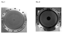
- FIG. 1 and No. 2 is a photograph showing the presence or absence of a black deposit in FIG.
- the inventors of the present invention will be described later as an oxide semiconductor thin film excellent in TFT mobility evaluated by high carrier mobility compared to a conventional In—Ga—Zn-based oxide semiconductor thin film (IGZO).
- IGZO In—Ga—Zn-based oxide semiconductor thin film
- An In—Ga—Sn-based oxide semiconductor thin film (IGTO) having a specific ratio of metal elements was invented and filed earlier.
- an oxide sintered body which is a material of a sputtering target used for manufacturing an In—Ga—Sn-based oxide semiconductor thin film (IGTO), is considered to be oxide sintered in the bonding process in consideration of productivity and manufacturing cost. It is also important to further suppress the cracking of the bonded body, and for that purpose, it is necessary to improve the oxide sintered body.
- IGTO In—Ga—Sn-based oxide semiconductor thin film
- the present inventors have studied an oxide sintered body, which is a material for an In—Ga—Sn-based sputtering target suitable for forming the oxide semiconductor thin film, in order to suppress cracking during bonding. It has been repeated.
- the oxide sintered body When the oxide sintered body is diffracted by X-ray diffraction, it has an effect of suppressing cracking of the oxide sintered body during bonding by controlling the proportion of the InGaO 3 phase; The effect of suppressing cracking of the oxide sintered body during bonding can be further improved by increasing the thickness of the oxide sintered body, and (c) the effect of suppressing cracking of the oxide sintered body when the average crystal grain size of the oxide sintered body is made finer. Has been found to be able to be further improved, leading to the present invention.
- the ratio of the content (atomic%) of each metal element (indium, gallium, tin) to the total metal elements excluding oxygen contained in the oxide sintered body is [In], [Ga], [ Sn], control is performed so as to satisfy the following formulas (1) to (3).
- [Ga] not only reduces oxygen deficiency, stabilizes the amorphous structure of the oxide semiconductor thin film, but also improves stress resistance (particularly resistance to light + negative bias stress). However, when [Ga] is too high, mobility decreases. Accordingly, [Ga] is 20 atom% or more, preferably 22 atom% or more, more preferably 24 atom% or more, and 30 atom% or less, preferably 29 atom% or less, more preferably 28 atom% or less. .
- [Sn] Sn / (In + Ga + Sn)) in all metal elements.
- [Sn] has an effect of improving chemical resistance of the oxide semiconductor thin film such as wet etching. However, since the etching rate becomes slower as the chemical resistance is improved, if [Sn] is too high, the etching processability is lowered. Accordingly, [Sn] is 25 atom% or more, preferably 26 atom% or more, more preferably 27 atom% or more, and 45 atom% or less, preferably 40 atom% or less, more preferably 35 atom% or less. .
- the metal element is composed of the above-mentioned ratios of In, Ga, and Sn, and does not contain Zn.
- the compositional deviation between the IGZO target and the IGZO film increases, and the surface of the IGZO target This is because it has been found that a black deposit composed of Zn and O is produced.
- the black deposit peels off from the target surface during sputtering and becomes particles, which causes arcing and causes a serious problem in film formation.
- the main reason why the above problem occurs when an IGZO target is used is that the vapor pressure of Zn is higher than that of Ga and In.
- Zn is reduced during the pre-sputtering, the vapor pressure of Zn is high, so that it easily evaporates and adheres to the target surface, producing a black deposit.
- compositional deviation between the target and the film is caused, and the atomic ratio of Zn in the film is greatly reduced as compared with the target.
- the oxide sintered body of the present invention is preferably composed of indium oxide satisfying the above-mentioned predetermined metal element content; gallium oxide; and tin oxide, and the remainder is an oxide that is inevitably produced in production. Impurities such as objects.
- the InGaO 3 phase detected when the oxide sintered body is X-ray diffracted will be described.
- the InGaO 3 phase is an oxide formed by combining In and Ga constituting the oxide sintered body of the present invention.
- the InGaO 3 phase has an effect of suppressing cracking due to stress during bonding in the oxide sintered body of the present invention.
- ICDD International Center for Diffraction Data
- ICDD International Center for Diffraction Data cards 21-0334, 71-2194, 77-0447 for diffraction peaks obtained by X-ray diffraction of the oxide sintered body. It has a crystal structure (corresponding to InGaO 3 phase, In 2 O 3 phase, and SnO 2 phase, respectively).
- the present invention is characterized in that when the oxide sintered body is subjected to X-ray diffraction, the InGaO 3 phase is contained at a predetermined ratio. If the peak intensity ratio ([InGaO 3 ]) of the InGaO 3 phase is small, the oxide sintered body is liable to crack during bonding, so it must be 0.05 or more. Preferably it is 0.06 or more, More preferably, it is 0.07 or more, More preferably, it is 0.1 or more.
- the upper limit is preferably as high as possible from the above viewpoint, and may be 1, for example, but considering the thermal equilibrium state, it is preferably 0.84 or less, more preferably 0.67 or less, and still more preferably 0.5. It is as follows.
- the InGaO 3 phase is a unique phase that is produced by manufacturing under predetermined sintering conditions described later, while the content of the metal element is controlled within the above range. Even when the types of metal elements constituting the oxide sintered body are the same, the crystal phases obtained are different when the content of metal elements and the production conditions are different. For example, the Ga 3-x n 5 + x Sn 2 O 16 phase formed in Patent Document 1 (In—Ga—Sn-based oxide sintered body) is not formed in the present invention.
- the crystal phases obtained also differ when the types of metal elements constituting the oxide sintered body are different.
- the (Ga, In) 2 O 3 phase formed in Patent Document 2 is similar in notation to the present invention, but is different from the ICDD card. It is a phase with a different crystal structure.
- the (Ga, In) 2 O 3 phase is not formed.
- the relative density of the oxide sintered body of the present invention is 90% or more. By increasing the relative density of the oxide sintered body, the effect of suppressing cracking during bonding can be further improved. In order to obtain such an effect, the oxide sintered body of the present invention needs to have a relative density of at least 90% or more, preferably 95% or more, and more preferably 98% or more.
- the upper limit is not particularly limited and may be 100%, but 99% is preferable in consideration of manufacturing costs.
- the average crystal grain size of the oxide sintered body crystal grains is refined. Specifically, a scanning electron microscope (SEM, Scanning Electron Microscope) in a fracture surface of an oxide sintered body (an oxide sintered body is cut in the thickness direction at an arbitrary position, and an arbitrary position on the cut surface).
- SEM Scanning Electron Microscope
- a preferable average crystal grain size is 8 ⁇ m or less, more preferably 6 ⁇ m or less.
- the lower limit of the average crystal grain size is not particularly limited, but the preferred lower limit of the average crystal grain size is about 0.05 ⁇ m from the balance between refinement of the average crystal grain size and production cost.
- the coarse crystal grains having a crystal grain size exceeding 15 ⁇ m cause cracking of the oxide sintered body at the time of bonding. Therefore, it is better that the coarse crystal grains are as small as possible, and the coarse crystal grains are preferably 10% or less, more preferably Is 8% or less, more preferably 6% or less, still more preferably 4% or less, and most preferably 0%.
- the oxide sintered body of the present invention is obtained by mixing and sintering indium oxide, gallium oxide, and tin oxide.
- the sputtering target of this invention can be manufactured by processing the said oxide sintered compact.
- the oxide powder was obtained by sintering by (a) mixing / pulverization ⁇ (b) drying / granulation ⁇ (c) preforming ⁇ (d) degreasing ⁇ (e) hot pressing.
- the oxide sintered body can be (f) processed ⁇ (g) bonded to obtain a sputtering target.
- the present invention is characterized in that (e) hot press sintering conditions are appropriately controlled as described in detail below, and other steps are not particularly limited, and usually used steps. It can be selected appropriately.
- this invention is not the meaning limited to this.
- indium oxide powder, gallium oxide powder, and tin oxide powder are mixed in a predetermined ratio, mixed and pulverized.
- the purity of each raw material powder used is preferably about 99.99% or more. This is because the presence of a small amount of an impurity element may impair the semiconductor characteristics of the oxide semiconductor thin film. It is preferable to control the blending ratio of each raw material powder to be within the above range.
- the mixing / pulverization is preferably performed by using a ball mill or a bead mill and adding the raw material powder together with water.
- the balls and beads used in these steps are preferably made of materials such as nylon, alumina, zirconia, and the like.
- a binder or a binder may be mixed in order to ensure the ease of the subsequent molding process.
- the mixing time is preferably 2 hours or more, more preferably 10 hours or more, and further preferably 20 hours or more.
- the powder after drying and granulation is filled in a mold having a predetermined size, and preformed by a mold press. This pre-molding is performed for the purpose of improving the handleability when being set in a predetermined mold in the hot press process, and therefore, a compact may be formed by applying a pressing force of about 49 to 98 MPa.
- the powder may be directly loaded into the mold and pressure-sintered without performing the preforming with a mold press.
- the heating conditions are not particularly limited as long as the purpose of degreasing can be achieved.
- the heating conditions may be maintained at about 500 ° C. in the atmosphere for about 5 hours.
- the molded body After degreasing, the molded body is set in a mold so that a desired shape is obtained.
- Sintering is performed by hot pressing.
- the mold during sintering either a mold or a graphite mold can be used depending on the sintering temperature, but it is preferable to use a graphite mold having excellent heat resistance at a high temperature of 900 ° C. or higher.
- the molded body is heated to a sintering temperature: 850 to 1250 ° C., and then sintered at a holding time at the temperature: 0.1 to 5 hours.
- a sintering temperature 850 to 1250 ° C.
- the sintering temperature is 850 ° C. or higher, preferably 875 ° C. or higher, more preferably 900 ° C. or higher, and 1250 ° C. or lower, preferably 1200 ° C. or lower.
- the holding time at the sintering temperature is too long, the crystal grains grow and become coarse, so that the average crystal grain size of the crystal grains cannot be controlled within a predetermined range.
- the holding time is too short, the above InGaO 3 phase cannot be formed in the above-mentioned proportion, and it cannot be sufficiently densified. Accordingly, the holding time is 0.1 hour or longer, preferably 0.5 hour or longer, and desirably 5 hours or shorter.
- the average rate of temperature rise up to the above sintering temperature is 600 ° C./hr or less after preforming.
- the average heating rate exceeds 600 ° C./hr, abnormal growth of crystal grains occurs, and the ratio of coarse crystal grains increases. Also, the relative density cannot be increased sufficiently.
- a more preferable average heating rate is 500 ° C./hr or less, and further preferably 400 ° C./hr or less.
- the lower limit of the average heating rate is not particularly limited, but is preferably 10 ° C./hr or more, more preferably 20 ° C./hr or more from the viewpoint of productivity.
- the pressurizing condition at the time of hot pressing is not particularly limited, but it is desirable to apply a pressure of 59 MPa or less, for example, a surface pressure (pressurizing pressure). If the pressure is too high, the graphite mold may be damaged, the densification promoting effect is saturated, and the press equipment must be enlarged. On the other hand, if the pressure is too low, densification may not proceed sufficiently.
- Preferable pressure conditions are 10 MPa or more and 39 MPa or less.
- the sintering atmosphere is preferably an inert gas atmosphere or a vacuum atmosphere in order to suppress oxidation and disappearance of graphite that is preferably used as a mold.
- the atmosphere control method is not particularly limited.
- the atmosphere may be adjusted by introducing Ar gas or N 2 gas into the furnace.
- the atmospheric gas pressure is preferably atmospheric pressure in order to suppress evaporation of a metal having a high vapor pressure.
- the oxide sintered body obtained as described above has a relative density of 90% or more.
- the sputtering target of the present invention is obtained by performing (f) processing ⁇ (g) bonding by a conventional method.
- the processing method of oxide sinter is not specifically limited, What is necessary is just to process to the shape according to various uses by a well-known method.
- a sputtering target can be manufactured by joining the processed oxide sintered body to a backing plate with a bonding material.
- the kind of material of the backing plate is not particularly limited, pure copper or copper alloy having excellent thermal conductivity is preferable.
- the type of the bonding material is not particularly limited, and various known bonding materials having electrical conductivity can be used. Examples thereof include an In-based solder material and an Sn-based solder material.
- the bonding method is also not particularly limited. For example, the oxide sintered body and the backing plate are heated and melted at a temperature at which the bonding material dissolves, for example, about 140 to 220 ° C., and the dissolved bonding material is applied to the bonding surface of the backing plate. And after bonding each bonding surface and crimping
- the sputtering target obtained by using the oxide sintered body of the present invention is free from cracking due to stress generated by impact or thermal history during bonding work, and has a very good specific resistance. Is 1 ⁇ ⁇ cm or less, more preferably 10 ⁇ 1 ⁇ ⁇ cm or less, and further preferably 10 ⁇ 2 ⁇ ⁇ cm or less.
- the sputtering target of the present invention it becomes possible to form a film that further suppresses abnormal discharge during sputtering and cracking of the sputtering target material, and physical vapor deposition (sputtering method) using the sputtering target is performed on the production line of the display device. It can be done efficiently.
- the obtained oxide semiconductor thin film also shows good TFT characteristics.
- Example 1 (Preparation of sputtering target) Table 1 shows indium oxide powder (In 2 O 3 ) having a purity of 99.99%, gallium oxide powder (Ga 2 O 3 ) having a purity of 99.99%, and tin oxide powder (SnO 2 ) having a purity of 99.99%. It mix
- a dispersing agent polycarboxylic acid ammonium
- the powder thus obtained was preformed with a die press under the following conditions, then heated to 500 ° C. under atmospheric pressure at atmospheric pressure, and held at that temperature for 5 hours for degreasing. (Preform conditions) Molding pressure: 1.0 ton / cm 2 When the thickness is t, the compact size: ⁇ 110mm x t13mm
- the obtained molded body was set in a graphite mold and hot pressed under the conditions A to F shown in Table 2. At this time, N 2 gas was introduced into the hot press furnace and sintered in an N 2 atmosphere.
- the obtained oxide sintered body was machined to finish ⁇ 100 mm ⁇ t5 mm. After heating the oxide sintered body and the Cu backing plate to 180 ° C. over 10 minutes, the oxide sintered body is bonded to the backing plate using a bonding material (indium) to produce a sputtering target. did.
- the relative density was determined by subtracting the porosity measured as follows. First, a sample was prepared by mirror-polishing the fracture surface of an oxide sintered body (the oxide sintered body was cut in the thickness direction at an arbitrary position, and the arbitrary position on the cut surface). Next, a photograph was taken at 1000 times using a scanning electron microscope (SEM), and the area ratio (%) of pores in a 50 ⁇ m square region was measured to obtain the porosity. About the said sample, the same operation was performed about 20 places in total and the average was made into the average porosity (%) of the said sample. The average relative density was calculated by [100 ⁇ average porosity], and the result is shown as “relative density (%)” in Table 4. In this example, the average relative density thus obtained was evaluated as 90% or more.
- the “average crystal grain size ( ⁇ m)” described in Table 4 was measured as follows. First, a sample was prepared by mirror-polishing the fracture surface of an oxide sintered body (the oxide sintered body was cut in the thickness direction at an arbitrary position, and the arbitrary position on the cut surface). Next, the structure was photographed with a scanning electron microscope (SEM) at a magnification of 400 times, a straight line having a length of 100 ⁇ m was drawn in an arbitrary direction, and the number of crystal grains contained in the straight line (N) The value calculated from [100 / N] was defined as the “crystal grain size on a straight line”.
- SEM scanning electron microscope
- the “ratio of coarse crystal grains (%)” shown in Table 4 was measured as follows. First, similarly to the above average crystal grain size, the fracture surface of the oxide sintered body is observed with an SEM, a straight line having a length of 100 ⁇ m is drawn in an arbitrary direction, and a crystal having a length of 15 ⁇ m or more cut on the straight line is drawn. The grains were coarse crystal grains. The length L of the coarse crystal grains occupying the straight line (when there are a plurality thereof, the sum thereof: ⁇ m) is obtained, and the value calculated from [L / 100] is used as the “ratio of coarse crystal grains on the straight line” ( %).
- ratio of coarse crystal grains on each straight line was calculated.
- ratio of coarse crystal grains of oxide sintered body (%).
- the oxide sintered body obtained in this way was evaluated as passing if the ratio of coarse crystal grains was 10% or less.
- InGaO 3 phase ratio “InGaO 3 phase (%)” shown in Table 4 was measured as follows. First, the sputtering target obtained by sputtering was removed from the backing plate, a 10 mm square test piece was cut out, and the intensity (diffraction peak) of the diffraction line of the crystal phase was measured and determined by the following X-ray diffraction.
- Analysis device “X-ray diffractometer RINT-1500” manufactured by Rigaku Corporation Analysis conditions: Target: Cu Monochromatic: Uses a monochrome mate (K ⁇ ) Target output: 40kV-200mA (Continuous firing measurement) ⁇ / 2 ⁇ scanning Slit: Divergence 1/2 °, Scattering 1/2 °, Received light 0.15 mm Monochromator light receiving slit: 0.6mm Scanning speed: 2 ° / min Sampling width: 0.02 ° Measurement angle (2 ⁇ ): 5 to 90 °
- the [InGaO 3 ] obtained in this way was evaluated as acceptable if it was 0.05 or more.
- the sputtering targets 1 to 6 were not subject to cracking during the bonding operation as well as during sputtering. Moreover, the relative density and specific resistance of the sputtering target thus obtained were also good.
- Sample No. 7 is an example using the steel type d of Table 1 which has a high ratio of [Sn] and does not satisfy the provisions of the present invention regarding the composition of the oxide sintered body.
- Table 4 the average crystal grain size was large, the preferred ratio of coarse crystal grains was high, and the peak intensity ratio of the InGaO 3 phase was also low.
- the oxide sintered body was cracked during the bonding operation.
- Sample No. 8 is an example in which the production condition D of Table 2 having a low holding temperature at the time of sintering was adopted, although the steel type a of Table 1 satisfying the provisions of the present invention was used as the composition of the oxide sintered body. As a result, as shown in Table 4, the relative density was lowered and the peak intensity ratio of the InGaO 3 phase was also low. In this example, the oxide sintered body was cracked during the bonding operation.
- Sample No. 9 the composition of the oxide sintered body used the steel type a in Table 1 that satisfies the provisions of the present invention, but the temperature rising rate to the sintering temperature is fast and the holding temperature during sintering is high.
- This is an example employing the manufacturing condition E.
- Table 4 the average crystal grain size was large and the preferable ratio of coarse crystal grains was high.
- the oxide sintered body was cracked during the bonding operation.
- Sample No. No. 10 is an example in which the production conditions F in Table 2 having a high holding temperature at the time of sintering were adopted, although the composition of the oxide sintered body used the steel type a in Table 1 that satisfies the provisions of the present invention. As a result, as shown in Table 4, the average crystal grain size was large and the preferable ratio of coarse crystal grains was high. In this example, the oxide sintered body was cracked during the bonding operation.
- Example 2 in order to demonstrate the usefulness of the In—Ga—Sn oxide sintered body (IGTO) defined in the present invention compared to the conventional In—Ga—Zn oxide sintered body (IGZO), The following experiment was conducted.
- IGTO In—Ga—Sn oxide sintered body
- IGZO In—Ga—Zn oxide sintered body
- DC (direct current) magnetron sputtering substrate temperature room temperature
- Deposition power density 2.5 W / cm 2
- Pre-sputtering time 10 minutes
- Table 1 shows indium oxide powder (In 2 O 3 ) having a purity of 99.99%, gallium oxide powder (Ga 2 O 3 ) having a purity of 99.99%, and zinc oxide powder (ZnO 2 ) having a purity of 99.99%. It mix
- the powder thus obtained was preformed with a die press under the following conditions, then heated to 500 ° C. under atmospheric pressure at atmospheric pressure, and held at that temperature for 5 hours for degreasing. (Preform conditions) Molding pressure: 1.0 ton / cm 2 When the thickness is t, the compact size: ⁇ 110mm x t13mm
- the obtained molded body was set in a graphite mold and hot pressed under the condition G shown in Table 2. At this time, N 2 gas was introduced into the hot press furnace and sintered in an N 2 atmosphere.
- the obtained oxide sintered body was machined to finish ⁇ 100 mm ⁇ t5 mm. After heating the oxide sintered body and the Cu backing plate to 180 ° C. over 10 minutes, the oxide sintered body is bonded to the backing plate using a bonding material (indium) to produce a sputtering target. did.
Abstract
Description
30原子%≦[In]≦50原子%・・・(1)
20原子%≦[Ga]≦30原子%・・・(2)
25原子%≦[Sn]≦45原子%・・・(3)
[InGaO3]≧0.05・・・(4)
但し、[InGaO3]=(I(InGaO3)/(I(InGaO3)+I(In2O3)+I(SnO2))
式中、I(InGaO3)、I(In2O3)、およびI(SnO2)はそれぞれ、X線回折で特定されたInGaO3相、In2O3相、SnO2相の回折強度の測定値である。
30原子%≦[In]≦50原子%・・・(1)
20原子%≦[Ga]≦30原子%・・・(2)
25原子%≦[Sn]≦45原子%・・・(3)
[InGaO3]≧0.05・・・(4)
但し、[InGaO3]=(I(InGaO3)/(I(InGaO3)+I(In2O3)+I(SnO2))
式中、I(InGaO3)、I(In2O3)、およびI(SnO2)はそれぞれ、X線回折で特定されたInGaO3相、In2O3相、SnO2相の回折強度の測定値を意味する。
(スパッタリングターゲットの作製)
純度99.99%の酸化インジウム粉末(In2O3)、純度99.99%の酸化ガリウム粉末(Ga2O3)、純度99.99%の酸化錫粉末(SnO2)を表1に示す質量比率および原子比率で配合し、水と分散剤(ポリカルボン酸アンモニウム)を加えてナイロンボールミルで20時間混合した。次に、上記工程で得られた混合粉末を乾燥して造粒を行った。
(予備成形の条件)
成形圧力:1.0ton/cm2
厚みをtとしたとき、成形体サイズ:φ110mm×t13mm
相対密度は、以下のようにして測定した気孔率を引き算することにより求めた。まず、酸化物焼結体の破断面(酸化物焼結体を任意の位置で厚み方向に切断し、その切断面表面の任意の位置)を鏡面研削した試料を用意した。次に、走査型電子顕微鏡(SEM)を用いて1000倍で写真撮影し、50μm角の領域に占める気孔の面積率(%)を測定して気孔率とした。上記試料について、同様の操作を合計20箇所について行い、その平均を当該試料の平均気孔率(%)とした。平均相対密度は、[100-平均気孔率]により算出し、その結果を表4に「相対密度(%)」として記載した。本実施例では、このようにして得られた平均相対密度が90%以上のものを合格と評価した。
表4に記載の「平均結晶粒径(μm)」は以下のようにして測定した。まず、酸化物焼結体の破断面(酸化物焼結体を任意の位置で厚み方向に切断し、その切断面表面の任意の位置)を鏡面研削した試料を用意した。次に、その組織を走査型電子顕微鏡(SEM)を用いて倍率400倍で写真撮影し、任意の方向で100μmの長さの直線を引き、この直線内に含まれる結晶粒の数(N)を求め、[100/N]から算出される値を当該「直線上での結晶粒径」とした。同様に粗大結晶粒が重複しない間隔(少なくとも20μm以上の間隔)で直線を20本作成して各直線上での結晶粒径を算出した。そして、[各直線上での結晶粒径の合計/20]から算出される値を「酸化物焼結体の平均結晶粒径」とした。本実施例では、このようにして得られた酸化物焼結体の平均結晶粒径が10μm以下のものを合格と評価した。
表4に記載の「粗大結晶粒の割合(%)」は以下のようにして測定した。まず、上記平均結晶粒径と同様、酸化物焼結体の破断面をSEM観察して、任意の方向に100μmの長さの直線を引き、この直線上で切り取られる長さが15μm以上の結晶粒を粗大な結晶粒とした。この粗大な結晶粒が直線上に占める長さL(複数ある場合はその総和:μm)を求め、[L/100]から算出される値を当該「直線上での粗大結晶粒の割合」(%)とした。同様に粗大結晶粒が重複しない間隔(少なくとも20μm以上の間隔)で直線を20本作成して各直線上での粗大結晶粒の割合を算出した。そして、[各直線上での粗大結晶粒の割合の合計/20]から算出される値を「酸化物焼結体の粗大結晶粒の割合」(%)とした。本実施例では、このようにして得られた酸化物焼結体の粗大結晶粒の割合が10%以下のものを合格と評価した。
表4に記載の「InGaO3相(%)」は以下のようにして測定した。まず、スパッタリングして得られたスパッタリングターゲットをバッキングプレートから取り外して10mm角の試験片を切出し、以下のX線回折により、結晶相の回折線の強度(回折ピーク)を測定して求めた。
分析装置:理学電機社製「X線回折装置RINT-1500」
分析条件:
ターゲット:Cu
単色化:モノクロメートを使用(Kα)
ターゲット出力:40kV-200mA
(連続焼測定)θ/2θ走査
スリット:発散1/2°、散乱1/2°、受光0.15mm
モノクロメータ受光スリット:0.6mm
走査速度:2°/min
サンプリング幅:0.02°
測定角度(2θ):5~90°
[InGaO3]=I(InGaO3)/(I(InGaO3)+I(In2O3)+I(SnO2))
表4に記載の「ボンディング時の割れ」の有無は以下のようにして測定した。上記機械加工した酸化物焼結体を加熱し、バッキングプレートにボンディングした後、酸化物焼結体表面に割れが生じていないか目視で確認した。酸化物焼結体表面に1mmを超えるクラックが確認された場合を「割れ」があると判断した。ボンディング作業を10回行い、1回でも割れがある場合を不合格と評価して、表4中に「有」と記載した。一方、10回中、1回も割れがない場合を合格と評価して、表4中に「無」と記載した。


本実施例では、従来のIn-Ga-Zn酸化物焼結体(IGZO)に比べて、本発明で規定するIn-Ga-Sn酸化物焼結体(IGTO)の有用性を実証するため、以下の実験を行った。
スパッタリング装置:株式会社アルバック製「CS-200」
DC(直流)マグネトロンスパッタリング法
基板温度:室温
(1)プリスパッタ
ガス圧:1mTorr
酸素分圧:100×O2/(Ar+O2)=0体積%
成膜パワー密度:2.5W/cm2
プリスパッタ時間:10分
(2)本成膜
ガス圧:1mTorr
酸素分圧:100×O2/(Ar+O2)=4体積%
成膜パワー密度:2.5W/cm2
膜厚:40nm
純度99.99%の酸化インジウム粉末(In2O3)、純度99.99%の酸化ガリウム粉末(Ga2O3)、純度99.99%の酸化亜鉛粉末(ZnO2)を表1に示す質量比率および原子比率で配合し、水と分散剤(ポリカルボン酸アンモニウム)とバインダーを加えてボールミルで20時間混合した。次に、上記工程で得られた混合粉末を乾燥して造粒を行った。
(予備成形の条件)
成形圧力:1.0ton/cm2
厚みをtとしたとき、成形体サイズ:φ110mm×t13mm


Claims (7)
- 酸化インジウムと;酸化ガリウムと;酸化錫とを焼結して得られる酸化物焼結体であって、
前記酸化物焼結体の相対密度が90%以上、
前記酸化物焼結体の平均結晶粒径が10μm以下であり、
前記酸化物焼結体に含まれる酸素を除く全金属元素に対する、インジウム、ガリウム、錫の含有量の割合(原子%)を夫々、[In]、[Ga]、[Sn]としたとき、下記式(1)~(3)を満足すると共に、
前記酸化物焼結体をX線回折したとき、InGaO3相は下記式(4)を満足するものであることを特徴とする酸化物焼結体。
30原子%≦[In]≦50原子%・・・(1)
20原子%≦[Ga]≦30原子%・・・(2)
25原子%≦[Sn]≦45原子%・・・(3)
[InGaO3]≧0.05・・・(4)
但し、[InGaO3]=(I(InGaO3)/(I(InGaO3)+I(In2O3)+I(SnO2))
式中、I(InGaO3)、I(In2O3)、およびI(SnO2)はそれぞれ、X線回折で特定されたInGaO3相、In2O3相、SnO2相の回折強度の測定値である。 - 前記酸化物焼結体の結晶粒径が15μmを超える粗大結晶粒の割合は10%以下である請求項1に記載の酸化物焼結体。
- 前記酸化物焼結体をX線回折したとき、Ga3-xn5+xSn2O16相は含まれないものである請求項1または2に記載の酸化物焼結体。
- 前記酸化物焼結体をX線回折したとき、(Ga、In)2O3相は含まれないものである請求項1または2に記載の酸化物焼結体。
- 請求項1または2に記載の酸化物焼結体を用いて得られるスパッタリングターゲットであって、比抵抗が1Ω・cm以下であることを特徴とするスパッタリングターゲット。
- 請求項1または2に記載の酸化物焼結体の製造方法であって、酸化インジウムと;酸化ガリウムと;酸化錫とを混合し、成形型にセットした後、焼結温度850~1250℃まで昇温した後、該温度域での保持時間0.1~5時間、加圧圧力59MPa以下で焼結することを特徴とする酸化物焼結体の製造方法。
- 前記焼結温度までの平均昇温速度が600℃/hr以下である請求項6に記載の酸化物焼結体の製造方法。
Priority Applications (3)
| Application Number | Priority Date | Filing Date | Title |
|---|---|---|---|
| KR1020157033548A KR101622530B1 (ko) | 2013-11-29 | 2014-11-28 | 산화물 소결체 및 스퍼터링 타깃, 및 그 제조 방법 |
| CN201480030142.0A CN105246855B (zh) | 2013-11-29 | 2014-11-28 | 氧化物烧结体和溅射靶、以及其制造方法 |
| US14/894,718 US10515787B2 (en) | 2013-11-29 | 2014-11-28 | Oxide sintered body and sputtering target, and method for producing same |
Applications Claiming Priority (2)
| Application Number | Priority Date | Filing Date | Title |
|---|---|---|---|
| JP2013247763 | 2013-11-29 | ||
| JP2013-247763 | 2013-11-29 |
Publications (1)
| Publication Number | Publication Date |
|---|---|
| WO2015080271A1 true WO2015080271A1 (ja) | 2015-06-04 |
Family
ID=53199206
Family Applications (1)
| Application Number | Title | Priority Date | Filing Date |
|---|---|---|---|
| PCT/JP2014/081642 WO2015080271A1 (ja) | 2013-11-29 | 2014-11-28 | 酸化物焼結体およびスパッタリングターゲット、並びにその製造方法 |
Country Status (6)
| Country | Link |
|---|---|
| US (1) | US10515787B2 (ja) |
| JP (1) | JP5796812B2 (ja) |
| KR (1) | KR101622530B1 (ja) |
| CN (1) | CN105246855B (ja) |
| TW (1) | TWI515167B (ja) |
| WO (1) | WO2015080271A1 (ja) |
Cited By (1)
| Publication number | Priority date | Publication date | Assignee | Title |
|---|---|---|---|---|
| JP2017019668A (ja) * | 2015-07-07 | 2017-01-26 | 株式会社コベルコ科研 | 酸化物焼結体およびスパッタリングターゲット、並びにそれらの製造方法 |
Families Citing this family (11)
| Publication number | Priority date | Publication date | Assignee | Title |
|---|---|---|---|---|
| JP6254308B2 (ja) | 2016-04-19 | 2017-12-27 | 株式会社コベルコ科研 | 酸化物焼結体およびスパッタリングターゲット、並びにそれらの製造方法 |
| US11728390B2 (en) * | 2017-02-01 | 2023-08-15 | Idemitsu Kosan Co., Ltd. | Oxide semiconductor film, thin film transistor, oxide sintered body, and sputtering target |
| JP6364561B1 (ja) * | 2017-05-18 | 2018-07-25 | 株式会社コベルコ科研 | 酸化物焼結体およびスパッタリングターゲット |
| JP6364562B1 (ja) * | 2017-05-19 | 2018-07-25 | 株式会社コベルコ科研 | 酸化物焼結体およびスパッタリングターゲット |
| CN107623040A (zh) * | 2017-09-05 | 2018-01-23 | 华南理工大学 | 一种铟镓锌氧化物薄膜晶体管及其制造方法 |
| JP6724057B2 (ja) * | 2018-03-30 | 2020-07-15 | Jx金属株式会社 | スパッタリングターゲット部材 |
| JP6722736B2 (ja) * | 2018-09-21 | 2020-07-15 | Jx金属株式会社 | 焼結体および、スパッタリングターゲット |
| TWI725685B (zh) * | 2018-12-28 | 2021-04-21 | 日本商出光興產股份有限公司 | 燒結體 |
| JP7250723B2 (ja) * | 2020-03-31 | 2023-04-03 | Jx金属株式会社 | スパッタリングターゲット及びスパッタリングターゲットの製造方法 |
| WO2023091330A1 (en) * | 2021-11-22 | 2023-05-25 | Corning Incorporated | Amorphous transparent conductive oxide films and methods of fabricating the same |
| CN116813310A (zh) * | 2023-06-01 | 2023-09-29 | 先导薄膜材料(广东)有限公司 | 一种稀土元素掺杂氧化铟锡镓靶材及其制备方法 |
Citations (3)
| Publication number | Priority date | Publication date | Assignee | Title |
|---|---|---|---|---|
| JP2000077358A (ja) * | 1998-08-27 | 2000-03-14 | Asahi Glass Co Ltd | 透明導電膜、スパッタリングターゲットおよび透明導電膜付き基体 |
| WO2011105047A1 (ja) * | 2010-02-24 | 2011-09-01 | 出光興産株式会社 | In-Ga-Sn系酸化物焼結体、ターゲット、酸化物半導体膜、及び半導体素子 |
| WO2013027391A1 (ja) * | 2011-08-22 | 2013-02-28 | 出光興産株式会社 | In-Ga-Sn系酸化物焼結体 |
Family Cites Families (7)
| Publication number | Priority date | Publication date | Assignee | Title |
|---|---|---|---|---|
| JP3457969B2 (ja) | 1992-05-11 | 2003-10-20 | 東ソー株式会社 | 高密度ito焼結体及びスパッタリングターゲット |
| US6042752A (en) * | 1997-02-21 | 2000-03-28 | Asahi Glass Company Ltd. | Transparent conductive film, sputtering target and transparent conductive film-bonded substrate |
| US20040222089A1 (en) * | 2001-09-27 | 2004-11-11 | Kazuyoshi Inoue | Sputtering target and transparent electroconductive film |
| JP5522889B2 (ja) | 2007-05-11 | 2014-06-18 | 出光興産株式会社 | In−Ga−Zn−Sn系酸化物焼結体、及び物理成膜用ターゲット |
| US20120279856A1 (en) * | 2009-10-15 | 2012-11-08 | Medvedovski Eugene | Tin Oxide Ceramic Sputtering Target and Method of Producing It |
| JP5883367B2 (ja) * | 2012-09-14 | 2016-03-15 | 株式会社コベルコ科研 | 酸化物焼結体およびスパッタリングターゲット、並びにその製造方法 |
| JP5883368B2 (ja) * | 2012-09-14 | 2016-03-15 | 株式会社コベルコ科研 | 酸化物焼結体およびスパッタリングターゲット |
-
2014
- 2014-11-28 US US14/894,718 patent/US10515787B2/en active Active
- 2014-11-28 KR KR1020157033548A patent/KR101622530B1/ko active IP Right Grant
- 2014-11-28 JP JP2014241480A patent/JP5796812B2/ja active Active
- 2014-11-28 CN CN201480030142.0A patent/CN105246855B/zh active Active
- 2014-11-28 WO PCT/JP2014/081642 patent/WO2015080271A1/ja active Application Filing
- 2014-12-01 TW TW103141601A patent/TWI515167B/zh active
Patent Citations (3)
| Publication number | Priority date | Publication date | Assignee | Title |
|---|---|---|---|---|
| JP2000077358A (ja) * | 1998-08-27 | 2000-03-14 | Asahi Glass Co Ltd | 透明導電膜、スパッタリングターゲットおよび透明導電膜付き基体 |
| WO2011105047A1 (ja) * | 2010-02-24 | 2011-09-01 | 出光興産株式会社 | In-Ga-Sn系酸化物焼結体、ターゲット、酸化物半導体膜、及び半導体素子 |
| WO2013027391A1 (ja) * | 2011-08-22 | 2013-02-28 | 出光興産株式会社 | In-Ga-Sn系酸化物焼結体 |
Cited By (1)
| Publication number | Priority date | Publication date | Assignee | Title |
|---|---|---|---|---|
| JP2017019668A (ja) * | 2015-07-07 | 2017-01-26 | 株式会社コベルコ科研 | 酸化物焼結体およびスパッタリングターゲット、並びにそれらの製造方法 |
Also Published As
| Publication number | Publication date |
|---|---|
| KR101622530B1 (ko) | 2016-05-18 |
| TW201538431A (zh) | 2015-10-16 |
| US20160111264A1 (en) | 2016-04-21 |
| TWI515167B (zh) | 2016-01-01 |
| US10515787B2 (en) | 2019-12-24 |
| CN105246855B (zh) | 2017-05-31 |
| CN105246855A (zh) | 2016-01-13 |
| KR20150136552A (ko) | 2015-12-07 |
| JP2015127293A (ja) | 2015-07-09 |
| JP5796812B2 (ja) | 2015-10-21 |
Similar Documents
| Publication | Publication Date | Title |
|---|---|---|
| JP5796812B2 (ja) | 酸化物焼結体およびスパッタリングターゲット、並びにその製造方法 | |
| JP5883367B2 (ja) | 酸化物焼結体およびスパッタリングターゲット、並びにその製造方法 | |
| JP5952891B2 (ja) | 酸化物焼結体、およびスパッタリングターゲットの製造方法 | |
| JP5883368B2 (ja) | 酸化物焼結体およびスパッタリングターゲット | |
| WO2012118156A1 (ja) | 酸化物焼結体およびスパッタリングターゲット | |
| TWI574935B (zh) | 氧化物燒結體、濺鍍用靶、及使用其而得之氧化物半導體薄膜 | |
| JP2012066968A (ja) | 酸化物焼結体およびスパッタリングターゲット | |
| JP6277977B2 (ja) | 酸化物焼結体、スパッタリング用ターゲット、及びそれを用いて得られる酸化物半導体薄膜 | |
| TWI557246B (zh) | An oxide sintered body, a sputtering target, and an oxide semiconductor thin film obtained therefrom | |
| TWI669283B (zh) | 氧化物燒結體及濺鍍靶材以及它們的製造方法 | |
| WO2013065784A1 (ja) | 酸化物焼結体およびスパッタリングターゲット、並びにその製造方法 | |
| TWI622568B (zh) | 氧化物燒結體及濺鍍用靶 | |
| JP6364561B1 (ja) | 酸化物焼結体およびスパッタリングターゲット | |
| JP2017019668A (ja) | 酸化物焼結体およびスパッタリングターゲット、並びにそれらの製造方法 | |
| JP6364562B1 (ja) | 酸化物焼結体およびスパッタリングターゲット | |
| JP5750064B2 (ja) | 酸化物焼結体およびスパッタリングターゲット |
Legal Events
| Date | Code | Title | Description |
|---|---|---|---|
| 121 | Ep: the epo has been informed by wipo that ep was designated in this application |
Ref document number: 14865778 Country of ref document: EP Kind code of ref document: A1 |
|
| ENP | Entry into the national phase |
Ref document number: 20157033548 Country of ref document: KR Kind code of ref document: A |
|
| WWE | Wipo information: entry into national phase |
Ref document number: 14894718 Country of ref document: US |
|
| NENP | Non-entry into the national phase |
Ref country code: DE |
|
| 122 | Ep: pct application non-entry in european phase |
Ref document number: 14865778 Country of ref document: EP Kind code of ref document: A1 |