WO2015072228A1 - スピン電子メモリ、情報記録方法及び情報再生方法 - Google Patents
スピン電子メモリ、情報記録方法及び情報再生方法 Download PDFInfo
- Publication number
- WO2015072228A1 WO2015072228A1 PCT/JP2014/074796 JP2014074796W WO2015072228A1 WO 2015072228 A1 WO2015072228 A1 WO 2015072228A1 JP 2014074796 W JP2014074796 W JP 2014074796W WO 2015072228 A1 WO2015072228 A1 WO 2015072228A1
- Authority
- WO
- WIPO (PCT)
- Prior art keywords
- layer
- spin
- alloy layer
- electronic memory
- recording
- Prior art date
- Legal status (The legal status is an assumption and is not a legal conclusion. Google has not performed a legal analysis and makes no representation as to the accuracy of the status listed.)
- Ceased
Links
Images



Classifications
-
- G—PHYSICS
- G11—INFORMATION STORAGE
- G11C—STATIC STORES
- G11C11/00—Digital stores characterised by the use of particular electric or magnetic storage elements; Storage elements therefor
- G11C11/56—Digital stores characterised by the use of particular electric or magnetic storage elements; Storage elements therefor using storage elements with more than two stable states represented by steps, e.g. of voltage, current, phase, frequency
- G11C11/5607—Digital stores characterised by the use of particular electric or magnetic storage elements; Storage elements therefor using storage elements with more than two stable states represented by steps, e.g. of voltage, current, phase, frequency using magnetic storage elements
-
- G—PHYSICS
- G06—COMPUTING OR CALCULATING; COUNTING
- G06F—ELECTRIC DIGITAL DATA PROCESSING
- G06F3/00—Input arrangements for transferring data to be processed into a form capable of being handled by the computer; Output arrangements for transferring data from processing unit to output unit, e.g. interface arrangements
- G06F3/06—Digital input from, or digital output to, record carriers, e.g. RAID, emulated record carriers or networked record carriers
- G06F3/0601—Interfaces specially adapted for storage systems
- G06F3/0602—Interfaces specially adapted for storage systems specifically adapted to achieve a particular effect
- G06F3/0625—Power saving in storage systems
-
- G—PHYSICS
- G06—COMPUTING OR CALCULATING; COUNTING
- G06F—ELECTRIC DIGITAL DATA PROCESSING
- G06F3/00—Input arrangements for transferring data to be processed into a form capable of being handled by the computer; Output arrangements for transferring data from processing unit to output unit, e.g. interface arrangements
- G06F3/06—Digital input from, or digital output to, record carriers, e.g. RAID, emulated record carriers or networked record carriers
- G06F3/0601—Interfaces specially adapted for storage systems
- G06F3/0628—Interfaces specially adapted for storage systems making use of a particular technique
- G06F3/0655—Vertical data movement, i.e. input-output transfer; data movement between one or more hosts and one or more storage devices
- G06F3/0659—Command handling arrangements, e.g. command buffers, queues, command scheduling
-
- G—PHYSICS
- G06—COMPUTING OR CALCULATING; COUNTING
- G06F—ELECTRIC DIGITAL DATA PROCESSING
- G06F3/00—Input arrangements for transferring data to be processed into a form capable of being handled by the computer; Output arrangements for transferring data from processing unit to output unit, e.g. interface arrangements
- G06F3/06—Digital input from, or digital output to, record carriers, e.g. RAID, emulated record carriers or networked record carriers
- G06F3/0601—Interfaces specially adapted for storage systems
- G06F3/0668—Interfaces specially adapted for storage systems adopting a particular infrastructure
- G06F3/0671—In-line storage system
- G06F3/0683—Plurality of storage devices
- G06F3/0688—Non-volatile semiconductor memory arrays
-
- G—PHYSICS
- G11—INFORMATION STORAGE
- G11C—STATIC STORES
- G11C11/00—Digital stores characterised by the use of particular electric or magnetic storage elements; Storage elements therefor
- G11C11/02—Digital stores characterised by the use of particular electric or magnetic storage elements; Storage elements therefor using magnetic elements
- G11C11/16—Digital stores characterised by the use of particular electric or magnetic storage elements; Storage elements therefor using magnetic elements using elements in which the storage effect is based on magnetic spin effect
- G11C11/161—Digital stores characterised by the use of particular electric or magnetic storage elements; Storage elements therefor using magnetic elements using elements in which the storage effect is based on magnetic spin effect details concerning the memory cell structure, e.g. the layers of the ferromagnetic memory cell
-
- G—PHYSICS
- G11—INFORMATION STORAGE
- G11C—STATIC STORES
- G11C11/00—Digital stores characterised by the use of particular electric or magnetic storage elements; Storage elements therefor
- G11C11/02—Digital stores characterised by the use of particular electric or magnetic storage elements; Storage elements therefor using magnetic elements
- G11C11/16—Digital stores characterised by the use of particular electric or magnetic storage elements; Storage elements therefor using magnetic elements using elements in which the storage effect is based on magnetic spin effect
- G11C11/165—Auxiliary circuits
- G11C11/1673—Reading or sensing circuits or methods
-
- G—PHYSICS
- G11—INFORMATION STORAGE
- G11C—STATIC STORES
- G11C11/00—Digital stores characterised by the use of particular electric or magnetic storage elements; Storage elements therefor
- G11C11/02—Digital stores characterised by the use of particular electric or magnetic storage elements; Storage elements therefor using magnetic elements
- G11C11/16—Digital stores characterised by the use of particular electric or magnetic storage elements; Storage elements therefor using magnetic elements using elements in which the storage effect is based on magnetic spin effect
- G11C11/165—Auxiliary circuits
- G11C11/1675—Writing or programming circuits or methods
-
- G—PHYSICS
- G11—INFORMATION STORAGE
- G11C—STATIC STORES
- G11C11/00—Digital stores characterised by the use of particular electric or magnetic storage elements; Storage elements therefor
- G11C11/18—Digital stores characterised by the use of particular electric or magnetic storage elements; Storage elements therefor using Hall-effect devices
-
- G—PHYSICS
- G11—INFORMATION STORAGE
- G11C—STATIC STORES
- G11C13/00—Digital stores characterised by the use of storage elements not covered by groups G11C11/00, G11C23/00, or G11C25/00
- G11C13/0002—Digital stores characterised by the use of storage elements not covered by groups G11C11/00, G11C23/00, or G11C25/00 using resistive RAM [RRAM] elements
- G11C13/0004—Digital stores characterised by the use of storage elements not covered by groups G11C11/00, G11C23/00, or G11C25/00 using resistive RAM [RRAM] elements comprising amorphous/crystalline phase transition cells
-
- G—PHYSICS
- G11—INFORMATION STORAGE
- G11C—STATIC STORES
- G11C13/00—Digital stores characterised by the use of storage elements not covered by groups G11C11/00, G11C23/00, or G11C25/00
- G11C13/04—Digital stores characterised by the use of storage elements not covered by groups G11C11/00, G11C23/00, or G11C25/00 using optical elements ; using other beam accessed elements, e.g. electron or ion beam
-
- H—ELECTRICITY
- H10—SEMICONDUCTOR DEVICES; ELECTRIC SOLID-STATE DEVICES NOT OTHERWISE PROVIDED FOR
- H10N—ELECTRIC SOLID-STATE DEVICES NOT OTHERWISE PROVIDED FOR
- H10N50/00—Galvanomagnetic devices
- H10N50/10—Magnetoresistive devices
-
- H—ELECTRICITY
- H10—SEMICONDUCTOR DEVICES; ELECTRIC SOLID-STATE DEVICES NOT OTHERWISE PROVIDED FOR
- H10N—ELECTRIC SOLID-STATE DEVICES NOT OTHERWISE PROVIDED FOR
- H10N50/00—Galvanomagnetic devices
- H10N50/80—Constructional details
-
- H—ELECTRICITY
- H10—SEMICONDUCTOR DEVICES; ELECTRIC SOLID-STATE DEVICES NOT OTHERWISE PROVIDED FOR
- H10N—ELECTRIC SOLID-STATE DEVICES NOT OTHERWISE PROVIDED FOR
- H10N50/00—Galvanomagnetic devices
- H10N50/80—Constructional details
- H10N50/85—Materials of the active region
-
- H—ELECTRICITY
- H10—SEMICONDUCTOR DEVICES; ELECTRIC SOLID-STATE DEVICES NOT OTHERWISE PROVIDED FOR
- H10N—ELECTRIC SOLID-STATE DEVICES NOT OTHERWISE PROVIDED FOR
- H10N70/00—Solid-state devices having no potential barriers, and specially adapted for rectifying, amplifying, oscillating or switching
- H10N70/20—Multistable switching devices, e.g. memristors
- H10N70/231—Multistable switching devices, e.g. memristors based on solid-state phase change, e.g. between amorphous and crystalline phases, Ovshinsky effect
- H10N70/235—Multistable switching devices, e.g. memristors based on solid-state phase change, e.g. between amorphous and crystalline phases, Ovshinsky effect between different crystalline phases, e.g. cubic and hexagonal
-
- H—ELECTRICITY
- H10—SEMICONDUCTOR DEVICES; ELECTRIC SOLID-STATE DEVICES NOT OTHERWISE PROVIDED FOR
- H10N—ELECTRIC SOLID-STATE DEVICES NOT OTHERWISE PROVIDED FOR
- H10N70/00—Solid-state devices having no potential barriers, and specially adapted for rectifying, amplifying, oscillating or switching
- H10N70/801—Constructional details of multistable switching devices
- H10N70/821—Device geometry
- H10N70/826—Device geometry adapted for essentially vertical current flow, e.g. sandwich or pillar type devices
-
- H—ELECTRICITY
- H10—SEMICONDUCTOR DEVICES; ELECTRIC SOLID-STATE DEVICES NOT OTHERWISE PROVIDED FOR
- H10N—ELECTRIC SOLID-STATE DEVICES NOT OTHERWISE PROVIDED FOR
- H10N70/00—Solid-state devices having no potential barriers, and specially adapted for rectifying, amplifying, oscillating or switching
- H10N70/801—Constructional details of multistable switching devices
- H10N70/881—Switching materials
- H10N70/882—Compounds of sulfur, selenium or tellurium, e.g. chalcogenides
- H10N70/8828—Tellurides, e.g. GeSbTe
Definitions
- the present invention relates to a spin electronic memory capable of memory operation of multi-value information using electron spin, an information recording method and an information reproducing method using the spin electronic memory.
- One solution is to operate the electronic device at an extremely low temperature to suppress the scattering of electrons.
- using a superconductor corresponds to that.
- the electron scattering is zero, so there is no electrical resistance and no Joule heat is generated. Therefore, the electron scattering does not occur.
- the electronic device when this method is used, the electronic device must be cooled to a temperature of several Kelvin, and the energy consumed for this purpose must not be forgotten.
- the topological insulator is an insulator that uses a special electronic state generated on the surface or interface of an object.
- the topological insulator is a relativistic phenomenon that occurs because the inner core electrons of an element with a relatively large atomic number move at a speed close to the speed of light. This will be explained based on the effect. In other words, this electron action (spin-orbit interaction) adds a term for the spin-orbit interaction to the Hamiltonian of the band structure formed by the electron, and changes the band structure and energy eigenvalue.
- the uppermost band of the valence band on the vacuum surface and the lowermost band of the conduction band are combined, but the band remains open inside the substance.
- a special band structure may be formed.
- a special physical property that has not been known so far appears which becomes a conductor on the surface or interface of the substance, but becomes an insulator because of a band inside.
- a substance having such characteristics is referred to as a “topological insulator” (see Non-Patent Document 1).
- the special electronic band structure possessed by the topological insulator is strange that electrons existing on the surface or interface of the material are separated into two electron spin currents with different spins and continue to flow without applying voltage due to time reversal symmetry. It has the characteristic. This is the same as having the important property of not being subjected to the electron scattering due to the impurities or the like if reversed. Also, for example, if there is no external magnetic field that breaks the time-reversal symmetry, this characteristic is preserved very firmly.
- the name of the topological insulator is derived from the fact that the characteristics of the electronic band structure are similar to the mathematical topology polyhedron theory (see Non-Patent Document 1).
- the present inventors have a crystal alloy layer composed of germanium-tellurium and a crystal alloy layer composed of antimony-tellurium for reducing the power consumption of the phase change solid-state memory regardless of the topological insulator.
- Proposed superlattice type phase change solid-state memory has been proposed (see Patent Documents 1 and 2 and Non-Patent Document 3).
- this superlattice phase change solid state memory can be an ideal topological insulator. This is because, as seen in Non-Patent Document 1, a crystal alloy layer (Sb 2 Te 3 crystal alloy layer) having an atomic ratio of antimony to tellurium of 2: 3 is used as the topological insulator, but the present inventor In the above proposal, a structure in which a plurality of crystal alloy layers are arranged and separated by a crystal alloy layer (GeTe crystal alloy layer) having a band gap of germanium and tellurium at a 1: 1 atomic ratio is exactly the above. This is because the recording layer of the superlattice phase change solid-state memory is used.
- a point (gamma point) in the reciprocal lattice space is crossed at one point so that the bottom band of the conduction band and the top band of the valence band are in contact with each other in the vicinity of the Fermi band.
- This phenomenon is a unique feature of the topological insulator, and this gamma point corresponds to the central symmetry point of the GeTe crystal alloy layer in real space. That is, it was confirmed that this layer was a non-scattering layer for the electrons, and that the electrons could move freely in two dimensions (see Patent Document 3).
- the inventors have found that the Sb 2 Te 3 crystal alloy layer has 1 It was found that the blocks do not show the band cross characteristic of the topological insulator, and that at least two blocks or more are necessary. However, in a layer thinner than two blocks, instead of becoming a topological insulator, the so-called Rashba effect appears in which the band degeneracy is resolved at the gamma point in the reciprocal lattice space and split into two spin bands having different energy states. I discovered that.
- the superlattice phase change film with the thickness of the Sb 2 Te 3 crystal alloy layer being changed is formed on a silicon wafer, an external magnetic field is applied in the direction perpendicular to the plane, and the split spin electron density is changed.
- the Rashba effect is remarkable in the case of the Sb 2 Te 3 crystal alloy layer thinner than 2 nm, and at a thickness larger than that, reflection due to spin splitting is observed. The difference in rate is small. In other words, it can be concluded that the superlattice phase change film having a thickness greater than this has a small Rashba effect and is the topological insulator.
- the stacked film including the GeTe crystal alloy layer and the Sb 2 Te 3 crystal alloy layer having a thickness of less than 2 nm becomes the spin current generation layer having the Rashba effect, and the GeTe crystal alloy layer has a thickness of 2 nm or more.
- the laminated film made of the Sb 2 Te 3 crystal alloy layer can be a spin current accumulation layer capable of accumulating a spin current.
- an object of the present invention is to provide a spin electronic memory capable of recording multi-value information and capable of greatly increasing the memory capacity, an information recording method and an information reproducing method using the spin electronic memory.
- Means for solving the problems are as follows. That is, ⁇ 1> A first electrode having at least a pair of electrodes and one of SbTe, Sb 2 Te 3 , BiTe, Bi 2 Te 3 , BiSe, and Bi 2 Se 3 and having a thickness of 2 nm to 10 nm. And a recording layer disposed between the electrodes, and a magnetic material, and a second alloy layer formed mainly of an alloy represented by the following general formula (1): And a spin injection layer for injecting spin into the recording layer in a state where the magnetic material is magnetized.
- M represents an atom of Ge, Al, or Si
- x represents a numerical value of 0.5 or more and less than 1.
- the spin electronic memory according to ⁇ 1> wherein at least two recording layers are stacked and arranged.
- the first alloy layer has a hexagonal crystal structure
- the second alloy layer has a cubic crystal structure
- the c-axis of the first alloy layer is oriented in the stacking direction.
- ⁇ 4> The spin electronic memory according to any one of ⁇ 1> to ⁇ 3>, wherein the second alloy layer is formed using GeTe as a main component.
- ⁇ 5> The spin electronic memory according to any one of ⁇ 1> to ⁇ 4>, wherein the thickness of the second alloy layer is more than 0 and 4 nm or less.
- ⁇ 6> Any one of the items ⁇ 1> to ⁇ 5>, which has an orientation layer that is arranged as a base of the second alloy layer and orients a laminated surface of the second alloy layer laminated thereon to a (111) plane.
- ⁇ 7> The spin electronic memory according to ⁇ 6>, wherein the orientation layer has the same composition as the first alloy layer and has the same crystal structure.
- ⁇ 8> The semiconductor device according to any one of ⁇ 1> to ⁇ 7>, wherein a magnetic field that forms a magnetic field perpendicular to the surface of the spin injection layer and has a magnetic part that injects spin into the recording layer through the spin injection layer.
- Spin electronic memory ⁇ 9> An information recording method using the spin electronic memory according to any one of ⁇ 1> to ⁇ 8>, wherein n is an integer of at least 1 and An information recording method comprising a step of applying a voltage at a voltage value divided into n steps as a voltage value necessary for accumulating spins in a saturated state for each recording layer.
- n is an integer of at least 1 and the resistance value of the n recording layers stacked
- An information reproducing method comprising the step of measuring any state value of light reflectance and determining the number of recording layers in which information is recorded among the recording layers according to the state value.
- the above-described problems in the prior art can be solved, multi-value information can be recorded, and the memory capacity can be greatly increased, an information recording method using the spin electronic memory, and An information reproducing method can be provided.
- the spin electronic memory of the present invention has at least a pair of electrodes, a recording layer, and a spin injection layer, and has members such as an alignment layer and a magnetic part as necessary.
- the recording layer is formed by laminating a first alloy layer and a second alloy layer, and is disposed between the pair of electrodes.
- This recording layer can accumulate spins for each layer, and the spin electronic memory can record and reproduce multi-value information according to the number of recording layers stacked. Therefore, the recording layer may be a single layer, but multi-level information of binary or higher can be recorded by laminating at least two or more layers.
- the first alloy layer is formed mainly of any one of SbTe, Sb 2 Te 3 , BiTe, Bi 2 Te 3 , BiSe, and Bi 2 Se 3 and has a thickness of 2 nm to 10 nm.
- the first alloy layer thus formed acts as the topological insulator, and the spin injected from the spin injection layer can be present on the surface or interface thereof.
- “main component” indicates an element that forms a basic unit cell of a layer.
- the first alloy layer is not particularly limited, but preferably has a hexagonal crystal structure and its c-axis is oriented in the stacking direction. With such a crystal structure, the next layer to be stacked serves as a template for generating orientation with this layer as a base, and a superlattice structure of these stacked bodies is easily obtained.
- the method for forming the first alloy layer is not particularly limited. However, since the c-axis oriented crystal structure can be easily obtained, for example, sputtering, molecular beam epitaxy, ALD (Atomic Layer Deposition), A CVD (Chemical Vapor Deposition) method or the like is preferable.
- the second alloy layer is formed mainly of an alloy represented by the following general formula (1).
- the second alloy layer has a phase difference between a first crystal phase having a structure having a space reversal symmetry at the center of the layer and a second crystal phase in which the space reversal symmetry is broken. It can be changed.
- the second crystal phase has the magnetic properties of a ferromagnetic material and can accumulate the spin.
- the second alloy layer can be changed in phase from the first crystal phase to the second crystal phase by applying a relatively weak voltage.
- the magnetic characteristics of the second alloy layer can be increased by applying a relatively strong voltage. It is possible to change the phase to the first crystal phase that is not present. By utilizing this characteristic, it is possible to perform a memory operation in which the second crystal phase capable of accumulating the spin is set in a set state and the first crystal phase in which the spin is released is reset.
- M represents an atom of Ge, Al, or Si
- x represents a numerical value of 0.5 or more and less than 1.
- GeTe is preferable because of its large dielectric constant.
- the thickness of the second alloy layer is not particularly limited, but is preferably more than 0 and 4 nm or less. When the thickness exceeds 4 nm, independent and unique characteristics may be exhibited, and the characteristics as the recording layer which is a laminated structure with the first alloy layer may be affected.
- the next layer to be stacked serves as a template for generating orientation with this layer as a base, and a superlattice structure of these stacked bodies is easily obtained.
- the method for forming the second alloy layer is not particularly limited, but a sputtering method, a molecular beam epitaxy method, an ALD method, a CVD method, and the like are preferable because the c-axis oriented crystal structure is easily obtained. .
- the spin injection layer is formed of a magnetic material, and is configured as a layer for injecting the spin into the recording layer in a state where the magnetic material is magnetized.
- the spin refers to spin-polarized electrons.
- a voltage is applied in a magnetized state, whereby the spin characteristics of electrons conducted to the recording layer are polarized by the magnetic material.
- the material used as a magnetic layer formation material of a well-known magnetic memory can be mentioned, Specifically, TbFeCo, FeCo, MnCr, MnPt etc. are mentioned.
- the thickness of the spin injection layer is not particularly limited, but is preferably 1 nm to 10 nm. If the thickness is less than 1 nm, sufficient spin orientation may not be obtained, and if it exceeds 10 nm, the magnetization becomes too strong and it may be difficult to erase data.
- the method for forming the spin injection layer is not particularly limited, and examples thereof include a sputtering method, a molecular beam epitaxy method, an ALD method, and a CVD method.
- the spin injection layer is disposed on the side where the electrode for allowing electrons to flow into the recording layer is disposed with respect to the recording layer in order to inject the spin into the recording layer. .
- Electrode> There is no restriction
- the electrode used for a well-known semiconductor element can be arranged and formed by a well-known method.
- the crystal structure of the first alloy layer is oriented in the c-axis, and the (111) plane of the crystal structure of the second alloy layer is oriented in a plane adjacent to the first alloy layer.
- the topological insulator and the phase change characteristic can be easily obtained.
- the first alloy layer can be easily obtained as a c-axis oriented body without any limitation on the base, but the superlattice structure can be obtained if the second alloy layer is not laminated with the c-axis oriented body as a base. Hateful.
- the second alloy layer when the second alloy layer is not formed using the first alloy layer as a base, the second alloy layer is disposed as a base of the recording layer (the second alloy layer). It is preferable to provide the orientation layer that orients the laminated surface of the second alloy layer to the (111) plane.
- the alignment layer is not particularly limited as long as it has such a role, but from the viewpoint of simplifying the manufacturing process, it has the same composition as the first alloy layer and has the same crystal structure. Is preferred. That is, the orientation layer is formed mainly of any one of SbTe, Sb 2 Te 3 , BiTe, Bi 2 Te 3 , BiSe and Bi 2 Se 3 , has a hexagonal crystal structure, and the crystal orientation Is preferably a crystal alloy layer oriented in the c-axis.
- the thickness of the alignment layer is preferably 3 nm or more, and more preferably 5 nm or more. When the thickness is less than 3 nm, the orientation strength to the c-axis may not be sufficiently obtained depending on the forming method.
- the orientation layer is used to stabilize the crystal structure of these layers. It is preferable that the second alloy layer is laminated with the substrate as a base.
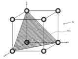
- FIGS. 1 (a) and 1 (b) are explanatory views showing the crystal structure of the first alloy layer of hexagonal crystal and the orientation layer
- FIG. 1B is the crystal of the second alloy layer of cubic crystal. It is explanatory drawing which shows a structure.
- the adjacent surface 51a becomes a hexagon. Therefore, when the cubic crystal alloy layer 52 is deposited as the second alloy layer on the surface of the crystal alloy layer 51, the (111) plane shown in FIG. 1B becomes the adjacent surface 52a. That is, since the cubic (111) plane is triangular, it aligns with the adjacent surface 52a of the c-axis oriented crystal alloy layer 51. Therefore, if a cubic crystal alloy layer 52 is deposited on the surface of the c-axis oriented crystal alloy layer 51, these adjacent surfaces 52a can be the (111) plane of the crystal alloy layer 52.
- the crystal alloy layer 52 is formed without the crystal alloy layer 51, the crystal alloy layer 52 is oriented, for example, in the (100) plane, and as a result, a superlattice formed of these laminates. Lattice disturbance is likely to occur in the structure.
- ⁇ Magnetic part> In the spin electron memory, from the viewpoint of injecting the spin into the recording layer, after forming the spin injection layer, a magnetic field perpendicular to the surface of the spin injection layer is applied to magnetize the spin injection layer. The role of aligning the spin orientation is imparted.
- the magnetic part may be disposed in the spin electronic memory, or may be removed after the spin injection layer is formed and its magnetization state is fixed. In the former case, further, from the viewpoint of reinforcing the strength of the magnetic field formed by the spin injection layer, by arranging as a layer laminated in parallel with the spin injection layer, the magnetized spin injection layer is The injection of the spin into the recording layer may be assisted.
- the magnetic part is configured as a magnetic layer that forms a magnetic field perpendicular to the surface of the spin injection layer and injects spins into the recording layer via the spin injection layer.
- the spin is injected into the recording layer by a magnetic field formed by the spin injection layer whose magnetization state is fixed.
- the magnetic part can comprise with a well-known permanent magnet, an electromagnet, etc.
- the spin electronic memory may have other members as necessary in addition to the orientation layer and the magnetic part.
- the other members are not particularly limited as long as the effects of the present invention are not impaired, and include members used in known semiconductor memories.
- a spin electronic circuit can be configured by integrating a plurality of the spin electronic memories. There is no restriction
- FIG. 2 is a cross-sectional view showing the layer configuration of the spin electronic memory according to one embodiment of the present invention.
- the spin electronic memory 10 has a configuration in which a semiconductor substrate 2, an alignment layer 3, three recording layers 6a to 6c, a spin injection layer 7, and a layered upper electrode 8 are arranged in this order on a layered lower electrode 1. Is done.
- Each of the three recording layers 6 a to 6 c has a structure in which the first alloy layer 5 is laminated on the second alloy layer 4.
- the configuration of the spin electronic memory 10 is an example, and the lower electrode 1 may be disposed on the semiconductor substrate 2, and the alignment layer 3 is disposed directly on the lower electrode 1 without using the semiconductor substrate 2. May be.
- the spin injection layer 7 may be disposed on the side where the upper electrode 8 for allowing electrons to flow into the recording layers 6a to 6c is disposed with respect to the recording layers 6a to 6c. May be disposed on the upper electrode 8.
- the first alloy layer 5 of the recording layers 6a to 6c acts as the topological insulator, and conducts the spin to the second alloy layer 4.
- the second alloy layer 4 has the first crystal phase composed of the structure having the spatial inversion symmetry at the center of the layer and the spatial inversion symmetry collapsed by the arrangement of germanium atoms, aluminum atoms, or silicon atoms. And having the second crystal phase.
- the inventor has found that the second crystal phase exhibits the Rashba effect and magnetic characteristics and acts as a ferromagnetic material capable of retaining the spin. Further, it was confirmed that a relatively weak voltage should be applied in order to preferentially express the second crystal phase.
- this voltage can be confirmed by measuring the characteristics in advance. Now, a relatively weak voltage is applied, the second alloy layer 4 in the mixed phase is brought into a state (set state) in which the second crystal phase is preferentially developed, and a voltage is applied to the spin electronic memory 10 from an external power source. Depending on the voltage value, electrons polarized by the spin injection layer 7 flow into the recording layers 6a to 6c, and spins can be accumulated in the recording layers 6a to 6c. This spin is held by the first alloy layer 5 acting as the topological insulator and the second alloy layer 4 in the set state.
- the accumulation of the spins in the recording layers 6a to 6c is started in order from the recording layer 6a closest to the electrode side into which electrons flow, and the accumulation of the spins in the recording layer 6a becomes saturated.
- the recording layer 6b is the next closest recording layer, and finally the recording layer 6c is used.
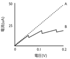
- FIG. 3A is an explanatory diagram for explaining current-voltage characteristics of a spin electronic memory according to an embodiment of the present invention
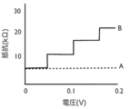
- FIG. 3B is a spin electronic memory according to an embodiment of the present invention. It is explanatory drawing explaining the resistance voltage characteristic.
- symbol A shows the characteristic when a magnetic field is not added
- symbol B shows the characteristic when a magnetic field is added.
- the current value increases in proportion to the voltage value, but in the characteristic indicated by the symbol B, the current value decreases stepwise as the voltage value increases. .
- the current value is stepped according to the stepwise accumulation of the spins in the recording layers 6a to 6c. Decline. Further, as shown in FIG. 3B, in the characteristic indicated by A, the resistance value increases in proportion to the voltage value, but in the characteristic indicated by B, the resistance value increases with increasing voltage value. It becomes the target. That is, when a magnetic field is applied by an electromagnet, the resistance value increases stepwise according to the stepwise accumulation of the spins in the recording layers 6a to 6c.
- the voltage applied to the recording layers 6 a to 6 c is set to a predetermined value by utilizing such a stepwise current value decrease phenomenon and a state value change phenomenon such as an increase in resistance value.
- the spin accumulation state is controlled so that multi-valued information can be recorded and reproduced.
- the recording layer is composed of three layers so that four-value information can be recorded / reproduced.
- the memory is multi-valued with a larger number. be able to.
- the spin electronic memory 10 by applying a relatively strong voltage, the second crystal phase of the second alloy layer 4 changes to the first crystal phase, and the magnetism is lost.
- the recording information in the recording layers 6a to 6c based on the accumulation state can be erased (reset state).
- This reset state can be returned to the set state by applying a relatively weak voltage again, and the spin electronic memory 10 can repeatedly record and erase information.
- the specific value of the voltage for the reset state can be confirmed by measuring the characteristics in advance.
- the information recording method of the present invention is an information recording method using the spin electronic memory, wherein n is an integer of at least 1 or more, and n layers of the recording layer are stacked for each recording layer. Including a step of applying a voltage with a voltage value divided into n steps as a voltage value necessary for accumulating in a saturated state.
- the spin electronic memory the spins are injected and accumulated in the order closest to the recording layer on the spin-in side. When the spin is saturated, the spin is accumulated in the next recording layer.
- the voltage for accumulating the spins in the respective recording layers in a saturated state can be grasped as a voltage value at each stage where a current-voltage characteristic is measured in advance and a stepwise decrease in current value occurs. Therefore, the voltage value of each step is divided into n steps according to the number of stacked recording layers, as a voltage value necessary for accumulating the spin in a saturated state for each layer of the recording layer, By applying a voltage with a voltage value, the spin can be selectively accumulated in the recording layer, and information corresponding to the number of recording layers can be recorded.
- the set state in which the recording can be performed can be made, and from the state in which the recording has been performed, the spin electronic memory can be made.
- a relatively strong voltage to the recording medium it is possible to obtain a reset state in which the recording is erased, and repetitive recording is possible.
- the information reproducing method of the present invention is an information reproducing method using the spin electronic memory, wherein n is an integer of at least 1 or any one of a resistance value and a light reflectance of the recording layer stacked by n layers. Measuring the state value and determining the number of the recording layers in which information is recorded among the recording layers according to the state value.
- the spin electronic memory can reproduce information from the spin accumulation state in the recording layer by the information recording method.
- the state in which information is recorded on the recording layer that is, the spin accumulation state, can be determined by the resistance value of the recording layer (see FIG. 3B) and the light reflectance.
- the recording layer in a state where information is recorded is measured. From the resistance value and the state value of the light reflectance, the voltage value corresponding to the state value, and further, the number of the recording layers on which the information is recorded are determined, and the information based on the number of layers is determined. Playback is possible. Note that when the resistance value is read as the state value, the voltage level applied to the spin electronic memory is sufficiently small so that the recording state of the recording layer is maintained at the time of reading, so that the recording level is the lowest. The resistance value is read out without affecting the spin accumulation state in the first-stage recording layer (the recording layer closest to the spin injection layer).
- sputtering is performed on a Si substrate having a clean surface using a sputtering apparatus (manufactured by ULVAC, helicon wave type sputtering apparatus) with Sb and Te as targets (composition ratio 2: 3), and Sb 2 Te.
- An alignment layer composed of three crystal alloy layers and having a c-axis crystal orientation aligned in the stacking direction was stacked with a thickness of 5 nm.
- sputtering using Ge and Te as a target (composition ratio 1: 1) is performed using the sputtering apparatus with the alignment layer as a base, and is composed of a crystalline alloy layer of GeTe.
- a second alloy layer oriented at a surface adjacent to the orientation layer was laminated with a thickness of 1 nm.
- sputtering is performed using the sputtering apparatus with Sb and Te as targets (composition ratio 2: 3), which is composed of a crystalline alloy layer of Sb 2 Te 3 and has a c-axis.
- a first alloy layer in which the crystal orientation was oriented in the stacking direction was stacked with a thickness of 5 nm.
- a layer formed by a laminated structure of the first alloy layer and the second alloy layer was used as a recording layer, and further, seven recording layers were formed, and a total of eight recording layers were laminated.
- the conditions for forming the alignment layer, the first alloy layer, and the second alloy layer were a vacuum state, and the sputtering temperature was 250 ° C.
- the crystal structure of the orientation layer, the first alloy layer, and the second alloy layer can be analyzed by comparing the first-principles calculation result based on the model and the X-ray diffraction result, and finally the cross section.
- sputtering using Te, Ge, and Co as targets composition ratio 1: 1: 1) is performed on the uppermost layer of the recording layer using the sputtering apparatus, and a TeFeCo crystal alloy layer as a spin injection layer A magnetic layer made of 2 nm in thickness was laminated.
- sputtering using Ti and N as a target (composition ratio 1: 1) was performed on the magnetic layer using the sputtering apparatus, and a TiN layer as an upper electrode was formed to a thickness of 40 nm. Further, a TiN layer as a lower electrode having a thickness of 40 nm was formed on the surface of the Si substrate opposite to the surface on which the alignment layer was laminated, in the same manner as the upper electrode. Thus, the spin electronic memory according to the example was manufactured.
- An external power source is connected to the spin electronic memory according to Example 1, a voltage is applied between the upper and lower electrodes, and the spin injection layer is magnetized by an electromagnet, and 0.4 T (Tesla) in the stacking direction of the recording layer.
- the current flowing through the memory was measured while gradually increasing the voltage value.
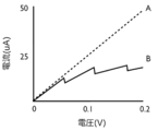
- the measurement result of this current-voltage characteristic is shown in FIG.
- symbol A indicates current-voltage characteristics when a 0.4 T magnetic field is not applied
- symbol B indicates current-voltage characteristics when a 0.4 T magnetic field is applied.
- FIG. 4 (a) when a 0.4T magnetic field is not applied (reference A in the figure), the current value increases in proportion to the increase in voltage value, but a 0.4T magnetic field is added.
- the symbol A indicates the current-voltage characteristic when a 0.4T magnetic field is not applied
- the symbol B indicates the current-voltage characteristic when a 0.4T magnetic field is applied.
- FIG. 4B when a 0.4T magnetic field is not applied (symbol A in the figure), the resistance value increases in proportion to the increase in voltage value, but a 0.4T magnetic field is added.
- the resistance value increased stepwise as the voltage value increased. This indicates that the spin is accumulated in a stepwise manner from the second alloy layer on the side close to the magnetic layer, as in FIG. There is a phenomenon that the resistance value increases according to the above.
- the number of spin-accumulated second alloy layers can be controlled, and the number of layers can be read from the resistance value of the memory. it can. As a result, it is possible to realize a memory for multilevel recording corresponding to the number of second alloy layers that are spin-accumulated, and to reproduce recorded multilevel information.
- the spin electronic memory according to the first embodiment can be a memory capable of repeatedly recording and reproducing multi-value information by repeating the set state and the reset state.
Landscapes
- Engineering & Computer Science (AREA)
- Computer Hardware Design (AREA)
- Theoretical Computer Science (AREA)
- Chemical & Material Sciences (AREA)
- Crystallography & Structural Chemistry (AREA)
- Human Computer Interaction (AREA)
- Physics & Mathematics (AREA)
- General Engineering & Computer Science (AREA)
- General Physics & Mathematics (AREA)
- Semiconductor Memories (AREA)
- Mram Or Spin Memory Techniques (AREA)
- Hall/Mr Elements (AREA)
Abstract
Description
このため、コンピューターには、冷却用のファンが必要である。また、前記ジュール熱によって入力エネルギーの一部が情報の記録・消去には利用できず、エネルギーロスが発生する。つまり、前記電子の散乱を抑制することが、前記電子デバイスの省電力化に向けた中心的な技術開発課題であることは疑う余地はない。
しかし、この方法を用いた場合には、前記電子デバイスを数ケルビンの温度まで冷却する必要があり、このために費やすエネルギーを忘れてはならない。また、このような極低温状態を利用する電子デバイスを一般化して実用化することは、困難である。そのため、室温で前記電子散乱を抑えられる手段としては、満足できるものが存在していない状況にある。
即ち、この電子の作用(スピン-軌道相互作用)によって、前記電子が形成するバンド構造のハミルトニアンにスピン-軌道相互作用の項が追加され、バンド構造とエネルギー固有値に変化が生じる。このとき、ある特殊な物質においては、真空表面での価電子帯の最上層部のバンドと伝導帯の最下部のバンドとが結合するが、他方、前記物質の内部ではバンドが開いたままの特殊なバンド構造が形成されることがある。
その結果、前記物質の表面あるいは界面では伝導体となるが、内部ではバンドがあるため絶縁体となるという、それまでに知られていなかった特殊な物性が出現する。このような特性をもつ物質を「トポロジカル絶縁体」と称す (非特許文献1参照)。
しかし、2ブロックより薄い層では、前記トポロジカル絶縁体にならない代わりに、逆格子空間内のガンマ点においてバンドの縮退が解れ、異なるエネルギー状態を持つ二つのスピンバンドに分裂する、いわゆるラシュバ効果が現れることを発見した。
この超格子型相変化膜がもつ前記ラシュバ効果は、これまで知られていた如何なる材料に比較して驚くほど大きく、前記第一原理計算によるシミュレーションでは、それらのスピンバンドの差で200meVにも達する。この大きさは、室温でさえスピン特性の違いを観測できるほど大きい(非特許文献4参照)。
つまり、前記GeTe結晶合金層と、厚みが2nmより薄い前記Sb2Te3結晶合金層からなる積層膜は、前記ラシュバ効果を持つスピン流発生層となり、前記GeTe結晶合金層と、厚みが2nm以上の前記Sb2Te3結晶合金層からなる積層膜は、スピン流を蓄積できるスピン流蓄積層となり得る。これらの二種類の結晶合金層を積層し、例えば、垂直方向に電場を加え、電子を注入すれば、スピン制御が可能であるばかりか、蓄積も可能なスピン電子メモリを提供できる(特許文献3参照)。
<1> 少なくとも、一対の電極と、SbTe、Sb2Te3、BiTe、Bi2Te3、BiSe及びBi2Se3のいずれかを主成分として形成され、厚みが2nm以上10nm以下である第1の合金層と、下記一般式(1)で表される合金を主成分として形成される第2の合金層とを積層させて形成され、前記電極間に配される記録層と、磁性材料で形成され、前記磁性材料が磁化された状態で前記記録層にスピンを注入するスピン注入層と、を有することを特徴とするスピン電子メモリ。
<2> 記録層が少なくとも2層以上積層されて配される前記<1>に記載のスピン電子メモリ。
<3> 第1の合金層が六方晶の結晶構造を有するとともに第2の合金層が立方晶の結晶構造を有し、前記第1の合金層のc軸が積層方向に配向され、前記第2の合金層の(111)面が前記第1の合金層との隣接面に配向される前記<1>から<2>のいずれかに記載のスピン電子メモリ。
<4> 第2の合金層がGeTeを主成分として形成される前記<1>から<3>のいずれかに記載のスピン電子メモリ。
<5> 第2の合金層の厚みが0を超え4nm以下である前記<1>から<4>のいずれかに記載のスピン電子メモリ。
<6> 第2の合金層の下地として配され、これに積層される前記第2の合金層の積層面を(111)面に配向させる配向層を有する前記<1>から<5>のいずれかに記載のスピン電子メモリ。
<7> 配向層が第1の合金層と同じ組成を有し、かつ、同じ結晶構造を有する前記<6>に記載のスピン電子メモリ。
<8> スピン注入層の面に対して垂直方向の磁場を形成し、前記スピン注入層を介して記録層にスピンを注入する磁性部を有する前記<1>から<7>のいずれかに記載のスピン電子メモリ。
<9> 前記<1>から<8>のいずれかに記載のスピン電子メモリを用いた情報記録方法であって、nを少なくとも1以上の整数として、n層積層される記録層に対し、前記記録層の一層ごとにスピンを飽和状態で蓄積させるのに必要な電圧値としてn段階の大きさに段階分けされた電圧値で電圧を加える工程を含むことを特徴とする情報記録方法。
<10> 前記<1>から<8>のいずれかに記載のスピン電子メモリを用いた情報再生方法であって、nを少なくとも1以上の整数として、n層積層される記録層の抵抗値及び光反射率のいずれかの状態値を測定し、前記状態値に応じて前記記録層のうち情報が記録された前記記録層の層数を判定する工程を含むことを特徴とする情報再生方法。
本発明のスピン電子メモリは、少なくとも、一対の電極と、記録層と、スピン注入層とを有し、必要に応じて、配向層、磁性部等の部材を有する。
前記記録層は、第1の合金層と、第2の合金層を積層させて形成され、前記一対の電極間に配される。この記録層は、一層ごとにスピンを蓄積させることができ、前記スピン電子メモリは、前記記録層の積層数に応じて多値の情報を記録し再生することができる。
したがって、前記記録層としては、1層であってもよいが、少なくとも2層以上積層することで2値以上の多値情報を記録することができる。
このように形成される前記第1の合金層は、前記トポロジカル絶縁体として作用し、前記スピン注入層から注入される前記スピンをその表面あるいは界面に存在させることができる。
なお、本明細書において「主成分」とは、層の基本単位格子を形成する元素であることを示す。
このような結晶構造を有すると、その次に積層される層が、この層を下地として配向を生み出すテンプレートとなって、これら積層体の超格子構造が得られやすい。
前記第1の合金層の形成方法としては、特に制限はないが、c軸配向の前記結晶構造が得られやすいことから、例えば、スパッタリング法、分子線エピタキシー法、ALD(Atomic Layer Deposition)法、CVD(Chemical Vapor Deposition)法などが好ましい。
この第2の合金層は、Mの配置によって、層の中心に空間反転対称性をもった構造からなる第1の結晶相と、前記空間反転対称性が崩れた第2の結晶相とに相変化可能とされる。前記第2の結晶相においては、強磁性体の磁気特性を有し、前記スピンを蓄積させることができる。
前記第2の合金層は、比較的弱い電圧を加えることで前記第1の結晶相から前記第2の結晶相に相変化可能とされる一方、比較的強い電圧を加えることで前記磁気特性のない第1の結晶相に相変化可能とされる。この特性を利用することで、前記スピンを蓄積可能な前記第2の結晶相をセット状態とし、前記スピンが解放された前記第1の結晶相をリセット状態としたメモリ動作が可能となる。

前記一般式(1)で表される合金としては、中でも、誘電率の大きさから、GeTeが好ましい。
前記厚みが4nmを超えると、独立した固有の特性を示すことがあり、前記第1の合金層との積層構造体である前記記録層としての特性に影響を及ぼすことがある。
このような結晶構造を有すると、その次に積層される層が、この層を下地として配向を生み出すテンプレートとなって、これら積層体の超格子構造が得られやすい。
前記第2の合金層の形成方法としては、特に制限はないが、c軸配向の前記結晶構造が得られやすいことから、例えば、スパッタリング法、分子線エピタキシー法、ALD法、CVD法等が好ましい。
前記スピン注入層は、磁性材料で形成され、前記磁性材料が磁化された状態で前記記録層に前記スピンを注入する層として構成される。なお、前記スピンとは、スピン偏極した電子を示し、前記スピン注入層では、磁化された状態で電圧を加えることにより、前記記録層に伝導される電子のスピン特性を前記磁性材料により偏極させる役割を持つ。
前記磁性材料としては、特に制限はなく、公知の磁性メモリの磁性層形成材料として用いられる材料を挙げることができ、具体的には、TbFeCo、FeCo、MnCr、MnPt等が挙げられる。これらは強磁性体であり、前記スピンの配向が磁性層としての前記スピン注入層の面に対して垂直となる磁場を形成し、前記スピン注入層と並行して配される前記記録層に対して、前記スピンの配向を揃えた状態で伝導させる目的として利用できる。
前記厚みが1nm未満であると、十分なスピン配向性が得られないことがあり、10nmを超えると、磁化が強くなり過ぎて、データの消去が困難となることがある。
また、前記スピン注入層の形成方法としては、特に制限はなく、スパッタリング法、分子線エピタキシー法、ALD法、CVD法等が挙げられる。
また、前記スピン注入層を配する位置としては、前記スピンを前記記録層に注入するため、前記記録層に対して、前記記録層に電子を流入させる前記電極が配される側に配される。
前記電極としては、特に制限はなく、目的に応じて適宜選択することができ、公知の半導体素子に用いられる電極を公知の方法により配して形成することができる。
前記スピン電子メモリにおいては、前記第1の合金層の結晶構造がc軸に配向され、前記第2の合金層の結晶構造の(111)面が前記第1の合金層との隣接面に配向される超格子構造を有すると、前記トポロジカル絶縁体及び前記相変化特性が得られやすい。
前記第1の合金層は、下地に制限なく、c軸配向体として得られやすいが、前記第2の合金層は、このc軸配向体を下地として積層させないと、前記超格子構造が得られにくい。 そのため、前記第2の合金層を前記第1の合金層を下地として形成しない場合には、前記記録層(前記第2の合金層)の下地として配され、これに積層される前記記録層の第2の合金層の積層面を(111)面に配向させる前記配向層を設けることが好ましい。
前記配向層の厚みとしては、3nm以上が好ましく、5nm以上がより好ましい。前記厚みが3nm未満であると、形成方法によっては、c軸への配向強度が十分に得られないことがある。
なお、こうした観点から、前記スピン電子メモリとしては、前記第1の合金層を下地として、前記第2の合金層を積層させるよりも、これらの層の結晶構造を安定化させるため、前記配向層を下地として前記第2の合金層を積層させて製造することが好ましい。
前記スピン電子メモリにおいては、前記スピンを前記記録層に注入する観点から、前記スピン注入層の形成後、前記スピン注入層の面に垂直の磁場を加えることで、前記スピン注入層を磁化させて、前記スピンの配向を揃える役割を付与する。この磁性部としては、前記スピン電子メモリに配することとしてもよいし、前記スピン注入層の形成後、その磁化状態を固定させた後、外してもよい。
前者の場合、更に、前記スピン注入層が形成する磁場の強さを補強する観点から、前記スピン注入層と並行して積層される層として配することで、磁化された前記スピン注入層の前記記録層に対する前記スピンの注入を補助させることとしてもよい。この場合、前記磁性部は、前記スピン注入層の面に対して垂直方向の磁場を形成し、前記スピン注入層を介して前記記録層にスピンを注入する磁性層として構成される。
また、後者の場合では、磁化状態が固定された前記スピン注入層が形成する磁場により前記スピンが前記記録層に注入される。
なお、前記磁性部としては、特に制限はなく、公知の永久磁石、電磁石等で構成することができる。
また、前記スピン電子メモリは、複数集積化させることで、スピン電子回路を構成することができる。前記スピン電子回路の回路構成としては、特に制限はなく、目的に応じて適宜選択することができ、公知の半導体回路を用いた回路構成とすることができる。
スピン電子メモリ10は、層状の下部電極1上に、半導体基板2、配向層3、3層の記録層6a~6c、スピン注入層7、層状の上部電極8がこの順で配された構成とされる。
また、3層の記録層6a~6cの各層は、第2の合金層4上に第1の合金層5が積層された構造とされる。
記録層6a~6cの第1の合金層5は、前記トポロジカル絶縁体として作用し、前記スピンを第2の合金層4に伝導させる。第2の合金層4は、ゲルマニウム原子、アルミニウム原子又はシリコン原子の配置によって、層の中心に前記空間反転対称性をもった構造からなる前記第1の結晶相と、前記空間反転対称性が崩れた前記第2の結晶相を有する。本発明者は、この第2の結晶相が前記ラシュバ効果や磁性特性を発現し、前記スピンを保持可能な強磁性体として作用することを見出した。また、前記第2の結晶相を優先的に発現させるためには、比較的弱い電圧を加えればよいことを確認した。この電圧の具体的な値は、予め特性を測定しておくことで確認することができる。
今、比較的弱い電圧を印加し、混合相の第2の合金層4を前記第2の結晶相が優先的に発現した状態(セット状態)とし、外部電源からスピン電子メモリ10に電圧を加えると、その電圧値に応じて、スピン注入層7によりスピン偏極された電子が記録層6a~6cに流入し、記録層6a~6cにスピンが蓄積可能とされる。このスピンは、前記トポロジカル絶縁体として作用する第1の合金層5及び前記セット状態の第2の合金層4により保持される。
この時、記録層6a~6cへの前記スピンの蓄積は、電子が流入される電極側に最も近い記録層6aから順々に開始され、記録層6aでの前記スピンの蓄積が飽和状態となると、次に近い記録層6bで行われ、最後に記録層6cで行われる。
図3(a)に示すように、符号Aの特性では、電圧値に比例して電流値が大きくなるが、符号Bの特性では、電圧値の上昇に対し、電流値が段階的に低下する。即ち、電磁石により、スピン注入層7を磁化させつつ、記録層6a~6cの積層方向に磁場を加えた場合、記録層6a~6cへの前記スピンの段階的な蓄積に応じて電流値が段階的に低下する。また、図3(b)に示すように、符号Aの特性では、電圧値に比例して抵抗値が大きくなるが、符号Bの特性では、電圧値の上昇に対し、抵抗値の上昇が段階的となる。即ち、電磁石により、磁場を加えた場合、記録層6a~6cへの前記スピンの段階的な蓄積に応じて抵抗値が段階的に増大する。
スピン電子メモリ10では、こうした段階的な電流値の低下現象、抵抗値の増大等の状態値変化現象を利用して、加える電圧を所定の値とすることで、記録層6a~6cへの前記スピンの蓄積状態を制御し、多値化された情報を記録再生可能とする。
なお、本例では、前記記録層を3層として4値の情報を記録再生可能な構成としたが、前記記録層の層数を増やすことで、より大きな数で多値化させたメモリとすることができる。
本発明の情報記録方法は、前記スピン電子メモリを用いた情報記録方法であって、nを少なくとも1以上の整数として、n層積層される前記記録層に対し、前記記録層の一層ごとにスピンを飽和状態で蓄積させるのに必要な電圧値としてn段階の大きさに段階分けされた電圧値で電圧を加える工程を含む。
図3(a)及び図3(b)を用いて説明したように、前記スピン電子メモリでは、前記スピンが流入される側の前記記録層から最も近い順に、前記スピンが注入され、蓄積した前記スピンが飽和状態となると、次に近い前記記録層で前記スピンが蓄積されていく。
この時、それぞれの前記記録層に前記スピンを飽和状態で蓄積させる電圧は、電流電圧特性を予め測定し、段階的な電流値の低下が生じる各段階の電圧値として把握することができる。
そこで、各段階の電圧値を前記記録層の一層ごとに前記スピンを飽和状態で蓄積させるのに必要な電圧値として、前記記録層の積層数に応じたn段階の大きさに段階分けし、電圧値で電圧を加えることで、前記記録層に対して選択的に前記スピンを蓄積させ、その記録層数に応じた情報を記録することが可能とされる。
なお、前記記録を行う前に、前記スピン電子メモリに比較的弱い電圧を加えることで、前記記録が可能なセット状態とすることができ、また、前記記録が行われた状態から前記スピン電子メモリに比較的強い電圧を加えることで、前記記録が消去されたリセット状態とすることができ、繰り返しの記録が可能とされる。
本発明の情報再生方法は、前記スピン電子メモリを用いた情報再生方法であって、nを少なくとも1以上の整数として、n層積層される前記記録層の抵抗値及び光反射率のいずれかの状態値を測定し、前記状態値に応じて前記記録層のうち情報が記録された前記記録層の層数を判定する工程を含む。
前記スピン電子メモリは、前記情報記録方法による前記記録層への前記スピンの蓄積状態から情報を再生することができる。
前記記録層に情報が記録された状態、即ち、前記スピンの蓄積状態は、前記記録層の前記抵抗値(図3(b)参照)や前記光反射率により判定することができる。即ち、予め、前記記録に用いた前記電圧値と、その時の前記記録層の前記抵抗値及び前記光反射率を対応させて測定しておくことにより、情報が記録された状態の前記記録層の前記抵抗値及び前記光反射率の状態値から、その状態値に対応した前記電圧値、延いては、前記情報が記録された前記記録層の層数を判定し、この層数に基づく情報の再生が可能とされる。
なお、前記状態値として、前記抵抗値を読み出す場合には、読み出し時に前記記録層の記録状態が保持されるよう、前記スピン電子メモリに加える電圧値を十分小さくすることで、記録レベルが最も小さい1段階目の前記記録層(前記スピン注入層に最も近い記録層)における前記スピンの蓄積状態に影響を与えない状態で前記抵抗値を読み出すようにする。
次に、前記配向層を下地として、前記スパッタリング装置を用いて、GeとTeをターゲット(組成比1:1)とするスパッタリングを行い、GeTeの結晶合金層からなり、結晶の(111)面が前記配向層との隣接面に配向された第2の合金層を1nmの厚みで積層させた。
次に、前記第2の合金層上に、前記スパッタリング装置を用いて、SbとTeをターゲット(組成比2:3)とするスパッタリングを行い、Sb2Te3の結晶合金層からなり、c軸の結晶方位が積層方向に配向された第1の合金層を5nmの厚みで積層させた。
これら第1の合金層と第2の合金層の積層構造で形成される層を記録層とし、更に、この記録層を7層形成して、合計8層の記録層を積層させた。
なお、前記配向層、前記第1の合金層及び前記第2の合金層を形成する条件としては、真空状態とし、スパッタ温度は、250℃とした。また、前記配向層、前記第1の合金層及び前記第2の合金層の結晶構造の解析は、モデルに基づく第一原理計算結果とX線回折結果を比較すること、また、最終的に断面を高分解能透過電子線像を撮影して観察することで行った。
次に、前記記録層の最上層上に、前記スパッタリング装置を用いて、TeとGeとCoをターゲット(組成比1:1:1)とするスパッタリングを行い、スピン注入層としてTeFeCoの結晶合金層からなる磁性層を2nmの厚みで積層させた。
次に、前記磁性層上に、前記スパッタリング装置を用いて、TiとNをターゲット(組成比1:1)とするスパッタリングを行い、上部電極としてのTiN層を40nmの厚みで形成した。また、前記Si基板の前記配向層が積層される面と反対側の面上に、前記上部電極と同様にして、下部電極としてのTiN層を40nmの厚みで形成した。
以上により、実施例に係るスピン電子メモリを製造した。
図4(a)に示されるように、0.4Tの磁場を加えない場合(図中の符号A)、電圧値の上昇に比例して電流値が上昇するが、0.4Tの磁場を加えた場合(図中の符号B)、電圧値の上昇に対し、段階的に電流値が上昇することが確認された。
このことは、先ず、スピンを注入する前記磁性層に最も近い前記記録層における前記第2の合金層にスピンが次第に蓄積し、そのスピンの蓄積が飽和すると、次に、2番目に近い前記第2の合金層にスピンが蓄積し、順次、前記磁性層に近い側の前記第2の合金層から段階的に前記スピンが蓄積されることを示している。即ち、一層の前記第2の合金層にスピン蓄積が飽和するごとに、段階的に電流値が一旦低下する現象が見られる。
また、この時の抵抗電圧特性の測定結果を図4(b)に示す。なお、図4(a)と同様に、符号Aは、0.4Tの磁場を加えない場合の電流電圧特性を示し、符号Bは、0.4Tの磁場を加えた場合の電流電圧特性を示す。
図4(b)に示されるように、0.4Tの磁場を加えない場合(図中の符号A)、電圧値の上昇に比例して抵抗値が上昇するが、0.4Tの磁場を加えた場合(図中の符号B)、電圧値の上昇に対し、段階的に抵抗値が上昇することが確認された。
このことは、図4(a)と同様に、前記磁性層に近い側の前記第2の合金層から段階的に前記スピンが蓄積されることを示しており、段階的に生じる電流値の低下に応じて、抵抗値が上昇する現象が見られる。
したがって、前記電極間に印加する電圧を一定の値とすることによって、スピン蓄積される第2の合金層の層数を制御することができ、その層数は、メモリの抵抗値から読み出すことができる。これにより、スピン蓄積される第2の合金層の層数に応じた多値記録のメモリを実現することができるとともに、記録された多値情報を再生することができる。
その後、改めて0.3Vで500nsの比較的弱い電流パルスを流し、前記第2の合金層が磁性特性を持つように相変化させたセット状態を回復させた。
次いで、前記セット状態の実施例1に係るスピン電子メモリに外部電源を接続し、上下電極間に0.15Vの電圧を加え、また、電磁石により、前記記録層の積層方向に0.4T(テスラ)の磁場を加えた後、電圧印加を停止した。
この状態から、電磁石をオフ状態とすることで該電磁石が形成する磁場を除いて、再び0.02Vの電圧を加えてメモリの抵抗値を測定したところ、図4(b)の測定結果と同様、0.15Vで磁場を加えたときに得られた16kΩの抵抗値が再び測定された。
したがって、実施例1に係るスピン電子メモリにおいては、前記セット状態、前記リセット状態を繰り返すことで多値情報を繰り返し記録再生可能なメモリとすることができる。
2 半導体基板
3 配向層
4 第2の合金層
5 第1の合金層
6a,6b,6c 記録層
7 スピン注入層
8 上部電極
10 スピン電子メモリ
Claims (10)
- 少なくとも、一対の電極と、
SbTe、Sb2Te3、BiTe、Bi2Te3、BiSe及びBi2Se3のいずれかを主成分として形成され、厚みが2nm以上10nm以下である第1の合金層と、下記一般式(1)で表される合金を主成分として形成される第2の合金層とを積層させて形成され、前記電極間に配される記録層と、
磁性材料で形成され、前記磁性材料が磁化された状態で前記記録層にスピンを注入するスピン注入層と、
を有することを特徴とするスピン電子メモリ。

- 記録層が少なくとも2層以上積層されて配される請求項1に記載のスピン電子メモリ。
- 第1の合金層が六方晶の結晶構造を有するとともに第2の合金層が立方晶の結晶構造を有し、前記第1の合金層のc軸が積層方向に配向され、前記第2の合金層の(111)面が前記第1の合金層との隣接面に配向される請求項1から2のいずれかに記載のスピン電子メモリ。
- 第2の合金層がGeTeを主成分として形成される請求項1から3のいずれかに記載のスピン電子メモリ。
- 第2の合金層の厚みが0を超え4nm以下である請求項1から4のいずれかに記載のスピン電子メモリ。
- 第2の合金層の下地として配され、これに積層される前記第2の合金層の積層面を(111)面に配向させる配向層を有する請求項1から5のいずれかに記載のスピン電子メモリ。
- 配向層が第1の合金層と同じ組成を有し、かつ、同じ結晶構造を有する請求項6に記載のスピン電子メモリ。
- スピン注入層の面に対して垂直方向の磁場を形成し、前記スピン注入層を介して記録層にスピンを注入する磁性部を有する請求項1から7のいずれかに記載のスピン電子メモリ。
- 請求項1から8のいずれかに記載のスピン電子メモリを用いた情報記録方法であって、
nを少なくとも1以上の整数として、n層積層される記録層に対し、前記記録層の一層ごとにスピンを飽和状態で蓄積させるのに必要な電圧値としてn段階の大きさに段階分けされた電圧値で電圧を加える工程を含むことを特徴とする情報記録方法。 - 請求項1から8のいずれかに記載のスピン電子メモリを用いた情報再生方法であって、
nを少なくとも1以上の整数として、n層積層される記録層の抵抗値及び光反射率のいずれかの状態値を測定し、前記状態値に応じて前記記録層のうち情報が記録された前記記録層の層数を判定する工程を含むことを特徴とする情報再生方法。
Priority Applications (3)
| Application Number | Priority Date | Filing Date | Title |
|---|---|---|---|
| JP2015547678A JP6124320B2 (ja) | 2013-11-15 | 2014-09-19 | スピン電子メモリ、情報記録方法及び情報再生方法 |
| KR1020167015846A KR101894828B1 (ko) | 2013-11-15 | 2014-09-19 | 정보 기록 장치, 정보 기록 방법 및 정보 재생 방법 |
| US15/036,666 US9984745B2 (en) | 2013-11-15 | 2014-09-19 | Spin electronic memory, information recording method and information reproducing method |
Applications Claiming Priority (2)
| Application Number | Priority Date | Filing Date | Title |
|---|---|---|---|
| JP2013236847 | 2013-11-15 | ||
| JP2013-236847 | 2013-11-15 |
Publications (1)
| Publication Number | Publication Date |
|---|---|
| WO2015072228A1 true WO2015072228A1 (ja) | 2015-05-21 |
Family
ID=53057172
Family Applications (1)
| Application Number | Title | Priority Date | Filing Date |
|---|---|---|---|
| PCT/JP2014/074796 Ceased WO2015072228A1 (ja) | 2013-11-15 | 2014-09-19 | スピン電子メモリ、情報記録方法及び情報再生方法 |
Country Status (5)
| Country | Link |
|---|---|
| US (1) | US9984745B2 (ja) |
| JP (1) | JP6124320B2 (ja) |
| KR (1) | KR101894828B1 (ja) |
| TW (1) | TWI598875B (ja) |
| WO (1) | WO2015072228A1 (ja) |
Cited By (4)
| Publication number | Priority date | Publication date | Assignee | Title |
|---|---|---|---|---|
| JP2017038032A (ja) * | 2015-08-14 | 2017-02-16 | 国立研究開発法人理化学研究所 | 電子デバイス、トポロジカル絶縁体、トポロジカル絶縁体の製造方法およびメモリ装置 |
| WO2019225160A1 (ja) * | 2018-05-23 | 2019-11-28 | 国立研究開発法人産業技術総合研究所 | スピン蓄積装置 |
| JPWO2020012916A1 (ja) * | 2018-07-10 | 2021-07-15 | 国立研究開発法人産業技術総合研究所 | 積層構造体及びその製造方法並びに半導体デバイス |
| JPWO2023012930A1 (ja) * | 2021-08-04 | 2023-02-09 |
Families Citing this family (8)
| Publication number | Priority date | Publication date | Assignee | Title |
|---|---|---|---|---|
| CN104392931B (zh) * | 2014-12-03 | 2018-06-22 | 京东方科技集团股份有限公司 | 薄膜晶体管及其制备方法、阵列基板、显示装置 |
| CN104362298B (zh) | 2014-12-03 | 2018-11-06 | 京东方科技集团股份有限公司 | 一种电极片及其制备方法、储能装置 |
| CN106960904B (zh) * | 2016-01-09 | 2019-05-31 | 清华大学 | 全相变自旋非易失存储单元 |
| DE102017122053A1 (de) * | 2017-09-22 | 2019-03-28 | Infineon Technologies Ag | Magnetisches Phasenwechselmaterial zur Wärmeabfuhr |
| US10405465B2 (en) * | 2017-11-16 | 2019-09-03 | The Boeing Company | Topological insulator thermal management systems |
| JP6487579B1 (ja) * | 2018-01-09 | 2019-03-20 | 浜松ホトニクス株式会社 | 膜厚計測装置、膜厚計測方法、膜厚計測プログラム、及び膜厚計測プログラムを記録する記録媒体 |
| US11176979B2 (en) | 2019-02-28 | 2021-11-16 | Regents Of The University Of Minnesota | Computational random access memory (CRAM) based on spin-orbit torque devices |
| CN111811701B (zh) * | 2020-07-20 | 2021-10-29 | 中国科学院重庆绿色智能技术研究院 | 一种多级微结构栅薄膜晶体管柔性压力传感器及其制备方法 |
Citations (3)
| Publication number | Priority date | Publication date | Assignee | Title |
|---|---|---|---|---|
| JP2011138924A (ja) * | 2009-12-28 | 2011-07-14 | Hitachi Ltd | 磁気メモリセル及び磁気メモリ |
| JP2013051245A (ja) * | 2011-08-30 | 2013-03-14 | Elpida Memory Inc | 結晶性化合物及びこれを用いた可変抵抗素子並びに電子デバイス |
| WO2013125101A1 (ja) * | 2012-02-21 | 2013-08-29 | 独立行政法人産業技術総合研究所 | スピン電子メモリ及びスピン電子回路 |
Family Cites Families (5)
| Publication number | Priority date | Publication date | Assignee | Title |
|---|---|---|---|---|
| JP4952985B2 (ja) * | 2006-08-10 | 2012-06-13 | 独立行政法人科学技術振興機構 | 磁気抵抗効果素子及び不揮発性ランダムアクセス磁気メモリ |
| JP4621897B2 (ja) | 2007-08-31 | 2011-01-26 | 独立行政法人産業技術総合研究所 | 固体メモリ |
| JP4635236B2 (ja) | 2008-10-30 | 2011-02-23 | 独立行政法人産業技術総合研究所 | 固体メモリの製造方法 |
| JP2014049497A (ja) * | 2012-08-29 | 2014-03-17 | Toshiba Corp | 不揮発性半導体記憶装置及びその動作方法 |
| EP2741295B1 (en) * | 2012-12-04 | 2016-03-02 | Imec | Spin transfer torque magnetic memory device |
-
2014
- 2014-09-19 KR KR1020167015846A patent/KR101894828B1/ko not_active Expired - Fee Related
- 2014-09-19 WO PCT/JP2014/074796 patent/WO2015072228A1/ja not_active Ceased
- 2014-09-19 US US15/036,666 patent/US9984745B2/en not_active Expired - Fee Related
- 2014-09-19 JP JP2015547678A patent/JP6124320B2/ja not_active Expired - Fee Related
- 2014-11-03 TW TW103138101A patent/TWI598875B/zh not_active IP Right Cessation
Patent Citations (3)
| Publication number | Priority date | Publication date | Assignee | Title |
|---|---|---|---|---|
| JP2011138924A (ja) * | 2009-12-28 | 2011-07-14 | Hitachi Ltd | 磁気メモリセル及び磁気メモリ |
| JP2013051245A (ja) * | 2011-08-30 | 2013-03-14 | Elpida Memory Inc | 結晶性化合物及びこれを用いた可変抵抗素子並びに電子デバイス |
| WO2013125101A1 (ja) * | 2012-02-21 | 2013-08-29 | 独立行政法人産業技術総合研究所 | スピン電子メモリ及びスピン電子回路 |
Non-Patent Citations (1)
| Title |
|---|
| JUNJI TOMINAGA: "Topological insulating and spin-properties emerged inGeTe/Sb_2Te_3 superlatticed phase change memory", ABSTRACTS OF THE MEETING OF THE PHYSICAL SOCIETY OF JAPAN, vol. 68, no. 2, 26 August 2013 (2013-08-26), pages 603 * |
Cited By (9)
| Publication number | Priority date | Publication date | Assignee | Title |
|---|---|---|---|---|
| JP2017038032A (ja) * | 2015-08-14 | 2017-02-16 | 国立研究開発法人理化学研究所 | 電子デバイス、トポロジカル絶縁体、トポロジカル絶縁体の製造方法およびメモリ装置 |
| WO2017029976A1 (ja) * | 2015-08-14 | 2017-02-23 | 国立研究開発法人理化学研究所 | 電子デバイス、トポロジカル絶縁体、トポロジカル絶縁体の製造方法およびメモリ装置 |
| WO2019225160A1 (ja) * | 2018-05-23 | 2019-11-28 | 国立研究開発法人産業技術総合研究所 | スピン蓄積装置 |
| JPWO2019225160A1 (ja) * | 2018-05-23 | 2020-12-17 | 国立研究開発法人産業技術総合研究所 | スピン蓄積装置 |
| JPWO2020012916A1 (ja) * | 2018-07-10 | 2021-07-15 | 国立研究開発法人産業技術総合研究所 | 積層構造体及びその製造方法並びに半導体デバイス |
| JP7416382B2 (ja) | 2018-07-10 | 2024-01-17 | 国立研究開発法人産業技術総合研究所 | 積層構造体及びその製造方法並びに半導体デバイス |
| JPWO2023012930A1 (ja) * | 2021-08-04 | 2023-02-09 | ||
| WO2023012930A1 (ja) * | 2021-08-04 | 2023-02-09 | 国立大学法人東北大学 | 相変化材料および相変化型メモリ素子 |
| JP7687722B2 (ja) | 2021-08-04 | 2025-06-03 | 国立大学法人東北大学 | 相変化材料および相変化型メモリ素子 |
Also Published As
| Publication number | Publication date |
|---|---|
| KR101894828B1 (ko) | 2018-09-04 |
| US20160284394A1 (en) | 2016-09-29 |
| JP6124320B2 (ja) | 2017-05-10 |
| US9984745B2 (en) | 2018-05-29 |
| KR20160086402A (ko) | 2016-07-19 |
| JPWO2015072228A1 (ja) | 2017-03-16 |
| TWI598875B (zh) | 2017-09-11 |
| TW201523604A (zh) | 2015-06-16 |
Similar Documents
| Publication | Publication Date | Title |
|---|---|---|
| JP6124320B2 (ja) | スピン電子メモリ、情報記録方法及び情報再生方法 | |
| JP6238495B2 (ja) | 結晶配向層積層構造体、電子メモリ及び結晶配向層積層構造体の製造方法 | |
| Zhang et al. | Recent progress and challenges in magnetic tunnel junctions with 2D materials for spintronic applications | |
| JP7227614B2 (ja) | 磁性体とBiSbの積層構造の製造方法、磁気抵抗メモリ、純スピン注入源 | |
| JP5750791B2 (ja) | スピン電子メモリ及びスピン電子回路 | |
| KR20220029381A (ko) | 쌍극자 결합 스핀 궤도 토크 구조 | |
| JP6424999B1 (ja) | スピン素子の安定化方法及びスピン素子の製造方法 | |
| EP3761384B1 (en) | Stabilization method for spin elements and production method for spin elements | |
| Liang et al. | Ruderman–Kittel–Kasuya–Yosida-type interlayer Dzyaloshinskii–Moriya interaction in synthetic magnets | |
| Cao et al. | Efficient tuning of the spin–orbit torque via the magnetic phase transition of FeRh | |
| Thapa et al. | A Review on Novel Low‐Dimensional Materials based Magnetic Tunnel Junctions: Opportunities, Challenges, and Applications | |
| JP6466564B2 (ja) | マルチフェロイック素子の初期化方法 | |
| TWI643367B (zh) | 形成磁性裝置的自由層的材料組成、自由層與磁性元件 | |
| JP2013051245A (ja) | 結晶性化合物及びこれを用いた可変抵抗素子並びに電子デバイス | |
| Zhao et al. | All two-dimensional van der Waals magnetic tunneling junctions | |
| CN117998970A (zh) | 磁性随机存取存储器堆叠体、其制造方法、和磁性随机存取存储器阵列 | |
| Noh et al. | DFT-NEGF Simulation Study of Co 2 FeAl-MgO-Co 2 FeAl Magnetic Tunnel Junctions Under Biaxial Strain | |
| CN117769902A (zh) | 通过使用播种自旋轨道扭矩切换磁性材料中的磁矩的方法 | |
| Li et al. | Electronic structures of ge2sb2te5/co2fex (x: Al, si) interfaces for phase change spintronics | |
| Rawal et al. | Spintronic Devices Based on Heterostructure Thin Films | |
| Thompson | Applications of Spin Polarization in Nanomaterials and Devices | |
| TW202437889A (zh) | 磁性隨機存取記憶體(mram)堆疊、其製造方法及mram陣列 | |
| KR20230145155A (ko) | 이방성 향상 더스트 층을 포함하는 전압 제어형 자기 이방성 메모리 디바이스 및 이를 형성하기 위한 방법들 | |
| Ionescu et al. | Study of the spin valves based on materials with high magnetocrystalline anisotropy used in spintronics |
Legal Events
| Date | Code | Title | Description |
|---|---|---|---|
| 121 | Ep: the epo has been informed by wipo that ep was designated in this application |
Ref document number: 14862876 Country of ref document: EP Kind code of ref document: A1 |
|
| ENP | Entry into the national phase |
Ref document number: 2015547678 Country of ref document: JP Kind code of ref document: A |
|
| WWE | Wipo information: entry into national phase |
Ref document number: 15036666 Country of ref document: US |
|
| NENP | Non-entry into the national phase |
Ref country code: DE |
|
| ENP | Entry into the national phase |
Ref document number: 20167015846 Country of ref document: KR Kind code of ref document: A |
|
| 122 | Ep: pct application non-entry in european phase |
Ref document number: 14862876 Country of ref document: EP Kind code of ref document: A1 |