WO2015072060A1 - バスバー、およびそれを用いた電力変換装置 - Google Patents
バスバー、およびそれを用いた電力変換装置 Download PDFInfo
- Publication number
- WO2015072060A1 WO2015072060A1 PCT/JP2014/004841 JP2014004841W WO2015072060A1 WO 2015072060 A1 WO2015072060 A1 WO 2015072060A1 JP 2014004841 W JP2014004841 W JP 2014004841W WO 2015072060 A1 WO2015072060 A1 WO 2015072060A1
- Authority
- WO
- WIPO (PCT)
- Prior art keywords
- electrode
- potential electrode
- bus bar
- switching element
- power conversion
- Prior art date
- Legal status (The legal status is an assumption and is not a legal conclusion. Google has not performed a legal analysis and makes no representation as to the accuracy of the status listed.)
- Ceased
Links
Images




Classifications
-
- H—ELECTRICITY
- H02—GENERATION; CONVERSION OR DISTRIBUTION OF ELECTRIC POWER
- H02M—APPARATUS FOR CONVERSION BETWEEN AC AND AC, BETWEEN AC AND DC, OR BETWEEN DC AND DC, AND FOR USE WITH MAINS OR SIMILAR POWER SUPPLY SYSTEMS; CONVERSION OF DC OR AC INPUT POWER INTO SURGE OUTPUT POWER; CONTROL OR REGULATION THEREOF
- H02M7/00—Conversion of AC power input into DC power output; Conversion of DC power input into AC power output
- H02M7/42—Conversion of DC power input into AC power output without possibility of reversal
- H02M7/44—Conversion of DC power input into AC power output without possibility of reversal by static converters
- H02M7/48—Conversion of DC power input into AC power output without possibility of reversal by static converters using discharge tubes with control electrode or semiconductor devices with control electrode
- H02M7/53—Conversion of DC power input into AC power output without possibility of reversal by static converters using discharge tubes with control electrode or semiconductor devices with control electrode using devices of a triode or transistor type requiring continuous application of a control signal
- H02M7/537—Conversion of DC power input into AC power output without possibility of reversal by static converters using discharge tubes with control electrode or semiconductor devices with control electrode using devices of a triode or transistor type requiring continuous application of a control signal using semiconductor devices only, e.g. single switched pulse inverters
- H02M7/5387—Conversion of DC power input into AC power output without possibility of reversal by static converters using discharge tubes with control electrode or semiconductor devices with control electrode using devices of a triode or transistor type requiring continuous application of a control signal using semiconductor devices only, e.g. single switched pulse inverters in a bridge configuration
-
- H—ELECTRICITY
- H02—GENERATION; CONVERSION OR DISTRIBUTION OF ELECTRIC POWER
- H02M—APPARATUS FOR CONVERSION BETWEEN AC AND AC, BETWEEN AC AND DC, OR BETWEEN DC AND DC, AND FOR USE WITH MAINS OR SIMILAR POWER SUPPLY SYSTEMS; CONVERSION OF DC OR AC INPUT POWER INTO SURGE OUTPUT POWER; CONTROL OR REGULATION THEREOF
- H02M1/00—Details of apparatus for conversion
- H02M1/32—Means for protecting converters other than automatic disconnection
- H02M1/34—Snubber circuits
- H02M1/348—Passive dissipative snubbers
Definitions
- the present disclosure relates to a bus bar and a power conversion device using the bus bar.
- Patent Document 1 discloses a power conversion device that includes two SW elements connected in series of an upper arm and a lower arm and converts the voltage and current from a DC power source to supply power to a load. ).
- the power conversion device disclosed in Patent Document 1 is a power conversion device used for an automobile motor drive device, and U, V, W as a bridge circuit including two SW elements connected in series of an upper arm and a lower arm. It is the power converter device provided with the three-phase inverter circuit.
- a square plate-like parallel conductor in which a positive electrode input terminal and a negative electrode input terminal are bonded together with an insulating film interposed therebetween is used as an input terminal.
- an input bus bar (hereinafter referred to as a positive input bus bar) constituting a part of the positive electrode side wiring and an input bus bar (hereinafter referred to as a negative input bus bar) constituting a part of the negative electrode side wiring, They are installed parallel to each other at a predetermined interval.
- the positive input bus bar has three-phase upper arm power semiconductor elements (SW elements) arranged at equal intervals, and the negative input bus bar has three phase lower arm power semiconductor elements (SW elements). It is arranged at equal intervals.
- the three-phase output bus bars are installed perpendicular to the positive and negative input bus bars so as to connect the upper arm and the lower arm of each phase. An alternating current is supplied to the load via the output bus bar.
- SW elements that supply power have a large current, high voltage, and high speed switching. (Hereinafter referred to as high-speed SW) is underway.
- SW loss switching loss
- SW loss switching loss
- the current increases, it is also necessary to improve the heat dissipation of the SW element.
- EMC heat dissipation of the SW element.
- the magnitude of the surge voltage due to the switching of the SW element is not only the SW element inside the module constituting the power conversion device and the smoothing capacitor on the DC power supply side, but also the floating voltage caused by the bus bar for electrically connecting them. It also depends on the inductance. When the value of the stray inductance is large, the surge voltage becomes high.
- each part constituting the positive electrode side wiring and each part constituting the negative electrode side wiring are constituted by flat parallel conductors as much as possible. It is effective to allow current to flow in the reverse direction. This is because it is possible to cause magnetic cancellation between the positive electrode side wiring and the negative electrode side wiring, and a reduction in inductance can be achieved.
- the area that is a flat parallel conductor is limited to the input terminal, and the reduction in inductance is insufficient.
- the positive input bus bar connected to the positive input terminal and the negative input bus bar connected to the negative input terminal are arranged at different positions in the plane, and are not formed as flat parallel conductors. For this reason, in the power converter device of patent document 1, the magnetic cancellation effect by a positive electrode input bus bar and a negative electrode input bus bar is small, and cannot reduce an inductance.
- the first object of the present disclosure is to provide a bus bar that can further suppress a surge voltage caused by switching of the SW element and ringing associated therewith.
- Another object of the present invention is to provide a power converter that can suppress surge voltage and ringing optimally using the bus bar.
- WHEREIN It has the 1st switching element which comprises an upper arm, and the 2nd switching element which comprises a lower arm, a 1st switching element and a 2nd switching element are connected in series, and it is from DC power supply.
- a bus bar having a planar shape is used for a power conversion device that converts a voltage and a current of the first switching element and supplies power to a load from a connection point of the first switching element and the second switching element and is resin-molded to constitute a module.
- One end connected to the high potential side of the DC power source, the other end connected to the positive electrode side of the first switching element, and one end connected to the low potential side of the DC power source Has a low potential electrode connected to the negative electrode side of the second switching element and an insulating layer.
- the high-potential electrode and the low-potential electrode are arranged so that at least a part thereof overlaps with each other in the thickness direction of the flat plate shape with an insulating layer interposed therebetween.
- a snubber circuit composed of a surface mount type capacitive element is electrically connected between the high potential electrode and the low potential electrode.
- the arrangement relationship between the high potential electrode and the low potential electrode in the flat bus bar is for reducing the inductance Ld of the power supply circuit and suppressing the surge voltage ⁇ V.
- the high-potential electrode and the low-potential electrode that are arranged so that at least part of them overlap each other have the current flowing in the opposite direction, and the effect of reducing inductance by canceling the magnetic flux occurs. Due to this inductance reduction effect, in the bus bar, the surge voltage ⁇ V can be suppressed by reducing the inductance Ld of the power supply circuit related to the bus bar. Further, since the magnetic energy stored in the inductance Ld is reduced, the resonance with the parasitic capacitance component hidden in the Ld path is quickly braked, and as a result, the period during which ringing occurs can be shortened.
- a snubber circuit composed of a surface-mount type capacitive element is electrically connected between the high potential electrode and the low potential electrode.
- the power conversion device includes a bus bar according to the first aspect, a first switching element, a second switching element, and a resin mold.
- the bus bar, the first switching element, and the second switching element are resin-molded into a flat rectangular parallelepiped shape so that a part of the high potential electrode and the low potential electrode are exposed, and the module is configured. .
- Part of the high-potential electrode and the low-potential electrode is drawn out from one side surface (S1) of the flat rectangular parallelepiped.
- the power conversion device using the bus bar described above can be a power conversion device that has excellent heat dissipation and can suppress surge voltage and ringing optimally as compared with conventional power conversion devices.
- FIG. 1 is an example of a patent-pending power converter, and is a circuit diagram of a power converter provided with a three-phase inverter circuit that drives a three-phase AC motor.
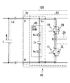
- FIG. 2 is a diagram illustrating an example of a bus bar according to the present disclosure and a power converter using the bus bar, and is a circuit diagram illustrating a part of the power converter using the bus bar.
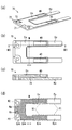
- FIG. 3A is a diagram showing a specific example of the bus bar 70 shown in FIG. 2, a perspective view showing the overall appearance of the bus bar, and FIG. 3B is a top view of the bus bar.
- FIG. 3 (c) is a cross-sectional view taken along the alternate long and short dash line IIIC-IIIC in FIG. 3 (b), and FIG. 3 (d) is a top view showing the positional relationship between the P electrode Ep and the N electrode En.
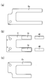
- 4A is an exploded top view showing the components of the bus bar shown in FIG. 3, which is a P electrode Ep, and FIG. 4B is an insulating layer and a surface-mount type capacitive element.
- 4 is a snubber circuit configured
- FIG. 4C is an N electrode En.
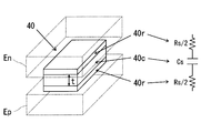
- FIG. 5 is a diagram showing an example of the snubber circuit configured by the surface-mount type capacitive element shown in FIG.
- FIG. 3 shows a perspective view of the structure of the snubber circuit connected between the P electrode Ep and the N electrode En.
- 6 (a) to 6 (d) are diagrams showing an example of a method for manufacturing the snubber circuit shown in FIG. 5, and are schematic perspective views for each manufacturing process.
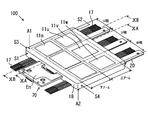
- FIG. 7 is a diagram showing a specific example of the power conversion device shown in the circuit diagram of FIG. 2, and is a perspective view showing an appearance of the resin-molded power conversion device using a bus bar
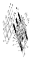
- FIG. 8 is an exploded perspective view showing each component before resin molding of the power conversion device shown in FIG.
- FIG. 9 is a diagram showing a final process of assembling each component shown in FIG.
- FIG. 8 is a diagram showing a state before assembling the heat sinks 11p, 11u to 11w at the top of the diagram
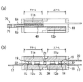
- FIG. 10A is a diagram schematically showing a cross section taken along the alternate long and short dash line XA-XA shown in FIG. 7
- FIG. 10B is a diagram schematically showing the cross section taken along the alternate long and short dash line XB-XB.
- FIG. 11A is a view showing a modification of the bus bar, which is a top view of the bus bar
- FIG. 11B is a cross-sectional view taken along one-dot chain line XIB-XIB in FIG.
- FIG. 12 is a view showing a modification of the bus bar and is a cross-sectional view of the bus bar.
- the semiconductor device has a semiconductor chip (SW element) for each of the upper arm and the lower arm, and a heat dissipating plate disposed on each of the front side and the back side of the semiconductor chip.
- SW element semiconductor chip
- the extraction conductor part which has the parallel conductor by which the positive electrode terminal and the negative electrode terminal were opposingly arranged on both sides of the insulating film.
- the positive terminal of the lead conductor is connected to the heat sink connected to the positive side of the semiconductor chip of the upper arm, and the negative terminal is connected to the heat sink connected to the negative side of the semiconductor chip of the lower arm.
- the resin mold part comprised so that a semiconductor chip might be covered, exposing one surface of a heat sink and a part of positive electrode terminal and negative electrode terminal is provided.
- the semiconductor device is excellent in heat dissipation, and the positive-side wiring and the negative-side wiring are configured with parallel conductors in a wider range, thereby further reducing the inductance. Yes.
- the present disclosure provides a new bus bar that can be applied to the power conversion device for which the above-mentioned patent application has been applied, and can further suppress a surge voltage caused by switching of the SW element and ringing associated therewith. Moreover, the power converter device which can suppress a surge voltage and ringing optimally using this bus bar is provided.
- the present disclosure relates to a bus bar and a power conversion device using the bus bar.
- the bus bar according to the present disclosure includes two SW elements connected in series of an upper arm and a lower arm, converts voltage and current from a DC power supply, and supplies power to a load from a connection point of the two SW elements. Used for power converters.
- the power conversion device to which the bus bar is applied is resin-molded to form a module.
- FIG. 1 is a circuit diagram of a power converter 90 provided with a three-phase inverter circuit 10 for driving a three-phase AC motor, which is an example of a patent-pending power converter described in the problem column.
- a power conversion device 90 surrounded by a dotted line in FIG. 1 includes an inverter circuit 10 surrounded by a one-dot chain line, and a bus bar 60 and an output terminal 20 surrounded by a two-dot chain line.
- the inverter circuit 10 converts the voltage and current from the DC power supply 2 and supplies power to the three-phase AC motor 3 that is a load.
- a DC power supply 2 and a smoothing capacitor 4 are connected in parallel to the inverter circuit 10 via a bus bar 60, and a constant power supply voltage is supplied while suppressing a reduction in ripple during switching and an influence of noise.
- the inverter circuit 10 has a configuration in which two SW elements 1H and 1L connected in series in an upper arm and a lower arm are connected in parallel for three phases.
- the SW elements 1H and 1L shown in the circuit diagram of FIG. 1 are IGBTs (insulated gate bipolar transistors), but MOSFETs (MOS field effect transistors) may be used.
- reflux FWDs (flywheel diodes) 2H and 2L are connected in antiparallel to the SW elements 1H and 1L, respectively. Then, the SW elements 1H and 1L of the upper and lower arms of each phase are controlled on and off in a predetermined order, and the intermediate potentials of the upper and lower arms are set to the U phase, V phase, and W phase of the three-phase AC motor 3. A three-phase alternating current is generated while sequentially switching to each phase. The generated three-phase AC current is output via the output terminal 20, and the three-phase AC motor 3 can be driven.
- the bus bar 60 is an input unit of the power converter 90 and inputs a constant power supply voltage via the DC power supply 2 and the smoothing capacitor 4 to the inverter circuit 10.
- the bus bar 60 includes a P terminal (high potential terminal) connected to the high potential side of the DC power supply 2 and an N terminal (low potential terminal) connected to the low potential side of the DC power supply 2.
- the P terminal is connected to the positive electrode side (+, high potential side) of the SW element 1H of the upper arm in the inverter circuit 10
- the N terminal is connected to the negative electrode side ( ⁇ , V) of the SW element 1L of the lower arm in the inverter circuit 10. Connected to the low potential side).
- the output terminal 20 is an output part of the power converter 90, and the three-phase alternating current generated by the inverter circuit 10 is transmitted from the terminals corresponding to the U-phase, V-phase, and W-phase to the three-phase. Supply to the AC motor 3.
- a portion surrounded by a one-dot chain line of reference numeral 10 includes a flat rectangular parallelepiped including the inverter circuit 10 and a part of the bus bar 60 and the output terminal 20 constituting the connection point with the inverter circuit 10 as described later. It is also a part that is resin-molded in the shape Therefore, the power conversion device 90 of FIG. 1 is a so-called 6-in-1 module in which six SW elements 1H and 1L of the U-phase, V-phase, and W-phase upper arm and lower arm are integrally molded by resin molding. is there.
- the circuit diagram of the power converter 90 shown in FIG. 1 has the following problems.
- the surge voltage ⁇ V generated in the power conversion device 90 of FIG. 1 has the relationship of the following formula 1 when the inductance of the power supply circuit indicated by the broken line in the drawing is Ld and the current change rate is dI / dt.
- the increase in power density (increase in current) and reduction in power loss (increase in high-speed SW) in the power conversion device described in the problem column are directions for increasing the current change rate dI / dt on the right side in Equation 1. Therefore, in order to suppress the surge voltage ⁇ V, it is necessary to make the inductance Ld of the power supply circuit as small as possible.
- the power conversion device 90 in which a patent application is pending, the arrangement relationship between the components of the power conversion device and the semiconductor chip on which the SW element is formed is fundamentally reviewed as will be described later. Then, the high potential electrode (hereinafter referred to as P electrode) and the low potential electrode (hereinafter referred to as N electrode) of the bus bar 60 are configured by parallel conductors in a wider range to reduce the inductance.
- the P electrode and the N electrode formed of parallel conductors have opposite current flow directions, and an inductance reduction effect due to magnetic flux cancellation occurs. Due to the effect of reducing the inductance, the power converter 90 can reduce the inductance Ld of the power supply circuit and suppress the surge voltage ⁇ V.
- the resonance with the parasitic capacitance component hidden in the Ld path is quickly braked, and the ringing suppression that shortens the period during which the ringing occurs is suppressed. An effect can be obtained.
- a snubber circuit before the inverter circuit 10 in order to further reduce the surge voltage caused by the switching of the SW element as well as the effect of reducing the inductance due to the magnetic flux cancellation.
- the portion surrounded by the alternate long and short dash line is resin-molded into a flat rectangular parallelepiped shape. Therefore, when a snubber circuit is additionally connected to the power converter 90 of FIG. 1, the following method is usually considered.
- This disclosure provides a novel bus bar in which a snubber circuit is built in the bus bar 60 of the power conversion device 90 shown in FIG.
- a bus bar with a built-in snubber circuit with different characteristics can be prepared in advance, and a power conversion device can be manufactured with a resin mold similar to the conventional one. Can do.
- FIG. 2 is a diagram illustrating an example of the bus bar according to the present disclosure and a power conversion device using the bus bar, and is a circuit diagram illustrating a part of the power conversion device 100 using the bus bar 70. 2 is obtained by replacing the bus bar 60 of the power conversion device 90 of FIG. 1 with a new bus bar 70. The same reference numerals are used for the same parts as those of the power conversion device 90 of FIG. Was attached.
- a bus bar 70 surrounded by a two-dot chain line in FIG. 2 includes a capacitor Cs and a resistor Rs (connected in two parts) connected in series to the bus bar 60 surrounded by a two-dot chain line in FIG.
- a snubber circuit 40 surrounded by a dotted line is additionally connected.
- the snubber circuit 40 built in the bus bar 70 in FIG. 2 is an RC snubber circuit in which a resistor Rs is connected in series to a capacitor Cs.
- the present invention is not limited to this, and is a C snubber circuit having only a capacitor Cs. However, the effect of reducing the constant surge voltage ⁇ V can be obtained. Further, it may be an RCD snubber circuit in which a diode is connected in parallel with the resistor Rs.
- the first term on the right side related to the inductance Ld of the power supply circuit is a term in ⁇
- the first term on the right side relates to the inductance Ls of the snubber circuit by using a capacitive element having a predetermined capacitance value. It can be smaller than the second term on the right side.
- the snubber circuit 40 built in the bus bar 70 is connected between the P electrode and the N electrode formed of parallel conductors in the vicinity of the inverter circuit 10. Therefore, as shown in FIG.
- Equation 2 since the length of the wiring (loop) is short, the inductance Ls of the snubber circuit is sufficiently smaller than the inductance Ld of the power circuit, and the second term on the right side of Equation 2 Is a value sufficiently smaller than the right side of Equation 1.
- the direction of current flow is reversed between the P electrode and the N electrode constituted by the parallel conductors of the bus bar 70, and the effect of reducing the inductance Ld due to magnetic flux cancellation described above occurs. ing. Therefore, the first term on the right side of Formula 2 can be made smaller than the second term with a capacitive element having a relatively small capacitance value Cs. Further, since the snubber circuit 40 is connected between the P electrode and the N electrode configured by the parallel conductors of the bus bar 70, the snubber circuit 40 can be configured with the shortest wiring length. As a result, the inductance Ls of the snubber circuit in the second term on the right side of Equation 2 can be minimized, and the effect of the snubber circuit connection can be maximized.
- the resistance value Rs of the resistor connected in series with the capacitive element there is an appropriate value for the resistance value Rs of the resistor connected in series with the capacitive element. If the resistance value Rs is too small, the surge to be reduced cannot be suppressed much. That is, since the parasitic inductance and the capacitive element of the snubber circuit alone do not consume current (stored as parasitic inductance), a resistor that consumes the current is required. Further, if the resistance value Rs is too small, there is a problem that the above-described LC resonance is likely to occur. On the other hand, if the resistance value Rs is too large, the surge generated in the SW element is not bypassed to the snubber circuit side, so that the snubber circuit does not function.
- the attenuation coefficient ⁇ of Equation 3 has a value of about 0.5 at which slight resonance occurs. preferable.
- FIG. 3A is a diagram showing a specific example of the bus bar 70 shown in FIG. 2, and is a perspective view showing the overall appearance of the bus bar 70.
- 3 (b) is a top view of the bus bar 70
- FIG. 3 (c) is a cross-sectional view taken along one-dot chain line IIIC-IIIC in FIG. 3 (b)
- FIG. It is the top view which showed the arrangement
- FIG. 4A is an exploded top view of the components of the bus bar 70 shown in FIG. 3 and shows a P electrode Ep, and FIG. 4B shows an insulating layer 71 and a surface mount type.
- FIG. 4C shows the N electrode En.
- the bus bar 70 shown in FIGS. 3 (a) to 3 (d) includes SW elements 1H and 1L in which an upper arm and a lower arm are connected in series. It is used in a power conversion device that converts voltage and current and supplies power to a load from a connection point of SW elements 1H and 1L.
- the bus bar 70 is formed in a U-shaped flat plate divided into two portions corresponding to a 6-in-1 module, which will be described later, and a P with an insulating layer 71 interposed therebetween. It has an electrode Ep and an N electrode En.
- the material of the insulating layer 71 that separates the P electrode Ep and the N electrode En is preferably made of a thermoplastic resin such as polyetheretherketone or liquid crystal polymer that is excellent in electrical insulation and easy to mold.
- the present invention is not limited to this, and it may be a thermosetting resin such as an epoxy resin, a ceramic material such as Al 2 O 3 , Si 3 N 4 , AlN, glass, or a mixed material in which a ceramic filler is mixed with an organic resin. May be.
- Each of the P electrode Ep and the N electrode En is made of a metal plate capable of passing a large current. In order to maximize the effect of reducing the inductance by canceling the magnetic flux, the P electrode Ep and the N electrode En The metal plates are arranged in parallel to each other.
- the P electrode Ep and the N electrode En are formed by using, for example, a material mainly composed of Cu, Al, Fe or the like and plating the surface for connection.
- one end of the P electrode Ep is connected to the high potential side of the DC power supply, and the other end is connected to the positive electrode side (+) of the SW element 1H of the upper arm.
- the portion surrounded by the alternate long and short dash line P1 is a portion connected to the positive electrode side (+) of the SW element 1H of the upper arm, and the portion surrounded by the alternate long and short dash line P2 This is the part connected to the potential side.
- the N electrode En has one end connected to the low potential side of the DC power supply and the other end connected to the negative electrode side ( ⁇ ) of the SW element 1L of the lower arm.
- the portion surrounded by the two-dot chain line N1 is a portion connected to the negative electrode side ( ⁇ ) of the SW element 1L of the lower arm, and the portion surrounded by the two-dot chain line N2 is a DC power source. It is a part connected to the low potential side.
- reference numeral 72 of the bus bar 70 shown in FIG. 3A is a through hole for positioning the P electrode Ep, the insulating layer 71, and the N electrode En at the time of manufacture, and reference numeral 73 is the P electrode Ep and the N electrode En. Is a through-hole for bolts for connecting to the respective wires on the DC power supply side.
- the P electrode Ep and the N electrode En are arranged so that at least a part thereof overlaps with each other in the thickness direction of the flat bus bar 70 with the insulating layer 71 interposed therebetween. Is arranged.
- the portion indicated by cross hatching is an overlapping region.
- the right side of the dotted line M is a portion that is resin-molded inside the module, and the left side of the dotted line M is a portion that is exposed to the outside of the module. is there.
- the U-shaped bus bar 70 is divided into two forks at the position covered with the mold resin.
- the bus bar 70 has the following configuration in order to reduce the inductance by configuring the P electrode Ep and the N electrode En as wide as possible with parallel conductors.
- the element-side P electrode portion Eps of the P electrode on the right side of the dotted line M resin-molded inside the module and the element-side N electrode portion Ens of the N electrode have different lengths. It has a strip shape.
- the shorter strip is arranged so as to overlap the longer strip with the insulating layer 71 interposed therebetween.
- the P electrode By arranging the SW elements of the upper arm and the lower arm along the long side direction of the element side P electrode portion Eps and the element side N electrode portion Ens which are arranged so as to overlap in this strip shape, the P electrode can be formed with the shortest length. And the N electrode can be pulled out. More specifically, the longer strip of the element-side P electrode portion Eps and the element-side N electrode portion Ens has a configuration in which the shorter strip is covered in the thickness direction. In the bus bar 70 shown in FIGS. 3A to 3D, the element side P electrode portion Eps which is a longer strip covers the element side N electrode portion Ens which is a shorter strip. According to this, the P electrode and the N electrode can be drawn out in a state where the parallel conductor range is maximized.
- the portion of the bus bar 70 exposed to the outside of the module on the left side of the dotted line M is configured such that the insulating layer 71 is slightly larger than the P electrode Ep and the N electrode En. ing.
- the outer edge portion of the P electrode Ep or N electrode En enters inside the outer edge portion of the insulating layer 71, and the insulating layer 71 protrudes from the P electrode Ep or N electrode En.
- the dimension design of the insulating layer 71 is to increase the creeping distance between the P electrode Ep and the N electrode En and improve the withstand voltage.
- the bus bar 70 has the following configuration in order to facilitate connection to the power supply side. As shown in FIG. 3 (d), in the thickness direction in the power supply side P electrode portion Epe of the P electrode on the left side of the dotted line M exposed to the outside of the module and the power supply side N electrode portion Ene of the N electrode, The cutouts Kp and Kn are provided so that parts do not overlap each other. A through hole 73 is formed in each of a part of the power supply side P electrode part Epe and a part of the power supply side N electrode part Epn that are configured not to overlap each other, and is connected to the DC power supply side using bolts and nuts. Wiring connection is possible.
- the snubber circuit 40 composed of the surface mount type capacitive element is formed in a part of the overlapping portion of the P electrode Ep and the N electrode En.
- the insulating layer 71 is inserted and electrically connected between the P electrode and the N electrode.
- the snubber circuit 40 may be disposed anywhere within the overlapping region shown by cross-hatching in FIG. 3D, and can be accommodated even when a large-capacity capacitive element is required because a large area can be obtained. It is.
- the snubber circuit 40 is preferably connected as close as possible to the SW elements 1H and 1L, and inside the module on the right side of the dotted line M in FIG. It is preferable to arrange in the part to be resin molded. Further, the snubber circuit 40 built in the flat bus bar 70 needs to be formed in a flat plate shape with a small thickness, as shown in FIG. Therefore, it is preferable that the surface-mount type capacitive element constituting the snubber circuit 40 has a flat rectangular parallelepiped shape with a small thickness aspect.
- symbol 74 of the insulating layer 71 shown in FIG.4 (b) is a through-hole formed in order to insert the snubber circuit 40.
- thermoplastic resin such as polyether ether ketone or liquid crystal polymer described above
- a metal paste or the like is applied to the upper and lower surfaces of the snubber circuit 40, and the bus bar 70 is formed by batch press firing. Can be manufactured.
- the bus bar 70 may be manufactured by a two-stage method in which a thermoplastic resin is injection molded using a mold after the snubber circuit 40 is connected between the P electrode Ep and the N electrode En by a metal paste or the like. Is possible.
- the bus bar 70 shown in FIGS. 3A to 3D is formed in a flat plate shape, and the P electrode Ep and the N electrode En have the insulating layer 71 in order to suppress the surge voltage.
- a structure in which at least a part of the layers overlaps each other in the thickness direction is adopted. That is, as shown in FIG. 3D, when the P electrode Ep and the N electrode En are projected onto one surface in the thickness direction of the flat bus bar 70, at least a part is overlapped.
- the arrangement relationship between the P electrode Ep and the N electrode En in the flat bus bar 70 is for reducing the surge voltage ⁇ V by reducing the inductance Ld of the power supply circuit described in Equation 1 of FIG. That is, the P electrode Ep and the N electrode En that are arranged so that at least a part thereof is overlapped with each other have opposite current flow directions in the overlapping portion, and an inductance reduction effect due to magnetic flux cancellation occurs. Due to this inductance reduction effect, in the bus bar 70, the inductance Ld of the power supply circuit can be reduced to suppress the surge voltage ⁇ V. Further, since the magnetic energy stored in the inductance Ld is reduced, the resonance with the parasitic capacitance component hidden in the Ld path is quickly braked, and as a result, the period during which ringing occurs can be shortened.
- the bus bar 70 shown in FIGS. 3A to 3D is configured by a surface-mount type capacitive element in place of the insulating layer 71 in a part of the overlapping portion of the P electrode Ep and the N electrode En.
- the snubber circuit 40 is electrically connected between the P electrode Ep and the N electrode En.
- the snubber circuit 40 is configured to connect the P electrode Ep and the N electrode En in the flat bus bar 70 with the shortest current path. Therefore, the inductance Ls of the snubber circuit 40 described in Equation 2 is also reduced, and the surge voltage ⁇ V is also suppressed by this.
- FIG. 5 is a diagram showing an example of a snubber circuit composed of the surface-mount type capacitive elements shown in FIGS. 3A to 3D, and is connected between the P electrode Ep and the N electrode En.
- 3 is a schematic perspective view showing the structure of the snubber circuit 40 in a perspective manner.
- 6 (a) to 6 (d) are diagrams showing an example of a method for manufacturing the snubber circuit 40 shown in FIG. 5, and are schematic perspective views according to manufacturing steps. 6A to 6D correspond to the state where the snubber circuit 40 shown in FIG. 5 is rotated by 90 °.
- the resistance layer 40r is laminated on the electrode layers (not shown) on both sides of the surface-mounted capacitive element 40c. As shown in the circuit diagram on the right side, the resistor Rs / 2 by the resistor layer 40r is connected in series to the capacitor Cs by the capacitor 40c.
- the capacitive element of the snubber circuit 40 built in the flat bus bar 70 shown in FIGS. 3A to 3D is a flat rectangular parallelepiped (thickness t) like the capacitive element 40c shown in FIG. It is preferable to form the electrode layer on both flat surfaces of the rectangular parallelepiped.
- a resistive layer is stacked on at least one electrode layer of the capacitive element as in the resistive layer 40r shown in FIG.
- the capacitance element 40c usually needs a capacitance value of about 0.05 to 0.5 ⁇ F.
- a capacitance value In order to earn a capacitance value, a large overlapping area of the P electrode Ep and the N electrode En of the bus bar 70 shown by cross hatching in FIG.
- the interval between the P electrode Ep and the N electrode En needs to be designed with a narrow gap.
- the snubber circuit 40 of the bus bar 70 has a configuration in which the cross-sectional area of the current path is large and the current path length is short. For this reason, the resistance value of the resistance layer 40r tends to be very small. Therefore, the material used for the resistance layer 40r is preferably a material having a specific resistance of 10 ⁇ 2 to 10 0 ⁇ m, and it is desirable to use a RuO 2 -based material or SnO 2 having a high glass ratio.
- the surge voltage ⁇ V It is equivalent as an effect of suppressing the above.
- a predetermined resistance value Rs is divided into two, and a resistance layer 40r having a resistance value of Rs / 2 is laminated on both electrode layers of the capacitive element 40c. It is preferable that the configuration is made. According to this, the heat generated in the two resistance layers 40r can be released to different P electrodes Ep and N electrodes En, respectively.
- the manufacturing method shown in FIGS. 6A to 6D can be employed.
- a dielectric sheet Lc on which the electrode layer Ei is printed is prepared, and the internal electrode layers Ei are alternately extended left and right. Laminate as follows.
- a titanium oxide system having a stable temperature and withstand voltage a barium titanate system having a high dielectric constant, or the like can be used.
- a Ni paste that can withstand baking at 1000 to 1300 ° C. can be used.
- the laminate is cut into a desired size (thickness t) and then baked.
- the electrode layer Eo is printed on the right and left of the said laminated body, and it bakes. As a result, the surface-mounted capacitive element 40c can be formed.
- the resistance layer 40r is printed on the fired electrode layer Eo and fired.
- a metal paste such as Cu that can withstand firing of the next resistance layer 40r can be used.
- a material having a high specific resistance such as RuO 2 or SnO 2 that can be fired at about 850 ° C. can be used.
- an electrode layer E is formed on the fired resistance layer 40r by vapor deposition, sputtering, plating, or the like. As a result, it is possible to serially connect a resistor composed of the resistance layer 40r to the capacitive element 40c.
- a metal suitable for connection with the P electrode material and the N electrode material is selected.
- the snubber circuit 40 having the structure of FIG. 5 can be manufactured.
- the manufacture of the snubber circuit 40 illustrated and described above uses an inorganic (ceramic) material. Not only this but the snubber circuit 40 which has the structure of FIG. 5 can also be manufactured even if it uses an organic (film) type material.
- an organic material such as a polyphenylene sulfide film is used as the dielectric sheet Lc shown in FIGS. 6A to 6D, and a low melting point metal such as Al is vapor-deposited as the electrode layer Ei to form a laminate.
- a polymer resistor paste that can be cured at low temperature can be used.
- a liquid material in which a metal thin film oxide can be obtained by firing using MOD metal organic compound decomposition method
- an MOD material dissolved in an organic solvent after an organic compound may be used.
- the MOD material includes TiO 2 as a dielectric and SnO 2 as a resistor. A large sheet (lamination) is formed using these, and these are cut and fired to obtain the structure of FIG.
- the snubber circuit 40 having the above can be manufactured.
- FIG. 7 is a diagram showing a specific example of the power conversion device 100 shown in the circuit diagram of FIG. 2, and is a perspective view showing the appearance of the resin-molded power conversion device 100 using the bus bar 70.
- FIG. 8 is an exploded perspective view showing each component before resin molding of the power conversion apparatus 100 shown in FIG.
- FIG. 9 is a diagram showing a final process of assembling each component shown in FIG. 8, and is a diagram showing a state before assembling the radiator plates 11p and 11u to 11w in the upper part of the figure. 8 and 9, the control terminal 17 is described as being integrated in a lead frame state, and the second heat radiation plates 12p, 12u, 12v, and 12w are also integrated. As shown in FIG. 7, the control terminal 17 is divided when the final product is formed, and each signal line becomes independent.
- FIG. 10A is a diagram schematically showing a cross section taken along the alternate long and short dash line XA-XA shown in FIG. 7, and FIG. 10B is a schematic diagram showing the cross section taken along the alternate long and short dash line XB-XB. It is the figure shown in.
- the mold resin 18 is indicated by a broken line in order to make the drawings easy to see.
- cross-sectional positions corresponding to FIGS. 7, 10 ⁇ / b> A, and 10 ⁇ / b> B are indicated by alternate long and short dashed lines XA-XA and alternate long and short dashed lines XB-XB, respectively.
- a power conversion device 100 shown in FIG. 7 is a power conversion device using the bus bar 70 of FIGS. 3 (a) to 3 (d).
- the P electrode Ep and the N electrode En of the bus bar 70 are partially exposed so that each of the U, V, and W phases shown in FIG.
- An inverter circuit 10 composed of six corresponding SW elements is resin-molded.
- the mold resin 18 is made of an insulating resin material such as an epoxy resin, and is formed by sealing (transferring) the component parts to be resin-molded in the mold.
- the mold resin 18 is formed into a flat rectangular parallelepiped shape and modularized. The interior of the mold resin 18 is partitioned into six blocks, each of which has six SW elements corresponding to the upper, lower, and U, V, and W phases, as indicated by the dotted lines in the figure. Yes.
- the power conversion device 100 shown in FIG. 7 includes a so-called 6-in-1 module in which each of U, V, and W phases and the six SW elements of the upper arm and the lower arm are integrated by resin molding. It has become.
- a part of the P electrode Ep and N electrode En of the bus bar 70 (the power supply side P electrode part Epe and the power supply side N electrode part En shown in FIG. 3D) is drawn out from one side surface S1 of the flat rectangular parallelepiped. It is.
- three output terminals 20 corresponding to the U, V, and W phases are drawn from the side face S2 facing the side face S1 from which the bus bar 70 is drawn.
- control terminals 17 for controlling the three SW elements 1L of the lower arm corresponding to the respective phases of U, V, and W are drawn out, and from the side surface S2, three of the upper arms are pulled out. Control terminals 17 for controlling the respective SW elements 1H are drawn out.
- the two SW elements 1H and 1L of the upper arm and the lower arm are along side surfaces S3 and S4 orthogonal to the side surface S1 from which the P electrode Ep and N electrode En of the bus bar 70 are drawn. They are arranged side by side.
- the P-electrode (element-side P-electrode portion) in the flat bus bar 70 is arranged along the direction in which the upper-arm SW element 1H and the lower-arm SW element 1L are aligned.
- Eps) and the N electrode (element side N electrode portion Ens) can be drawn out. Thereby, the range which comprises the P electrode Ep and the N electrode En by a parallel conductor can be maximized.
- one surface of the first heat radiation plates 11u, 11v, 11w, and 11n is exposed on the upper surface A1 of the mold resin 18 formed into a flat rectangular parallelepiped.
- the 1st heat sink 11u, 11v, 11w of an upper arm is made into a different body in each phase of U, V, W, and the 1st heat sink 11n of a lower arm is U , V, W are integrated heat sinks.
- Output terminals 20 of U, V, and W phases are drawn out from the first heat radiation plates 11u, 11v, and 11w of the upper arm, respectively.
- the second heat radiating plate 12p of the upper arm is an integrated heat radiating plate that connects the U, V, and W phases, and the second heat radiating plates 12u, 12v, 12w of the lower arm are used. Are separated from each other in U, V and W phases.
- the second heat dissipating plate 12p of the upper arm and the first heat dissipating plate 11n of the lower arm are each formed as an integrated heat dissipating plate that connects the U, V, and W phases. Not only this but the 2nd heat sink of an upper arm and the 1st heat sink of a lower arm should also be electrically connected. You may make it comprise as a separate heat sink for every U, V, and W phase.
- the first heat radiation plates 11u, 11v, 11w, and 11n and the second heat radiation plates 12p, 12u, 12v, and 12w correspond to heat sinks.
- a material mainly composed of Cu, Al, Fe, or the like is used on the surface. It is formed by plating for connection.
- the module of the power converter 100 employs the following configuration.
- a negative electrode and a control pad are formed on the first surface (upper surface in the figure) of the semiconductor chip, and a positive electrode is formed on the second surface (lower surface in the figure).
- the formed vertical element is adopted.
- the negative electrode is the source of the MOSFET and the emitter of the IGBT
- the positive electrode is the drain of the MOSFET and the collector of the IGBT
- the control pad is a wiring connected to the gate electrode.
- the semiconductor chips of the SW elements 1H and 1L are formed using Si, SiC, GaN or the like as a base material substrate. Each of the semiconductor chips of the SW elements 1H and 1L is between the first heat radiation plates 11u, 11v, 11w, and 11n exposed on the upper surface A1 of the mold resin 18 and the second heat radiation plates 12p, 12u, 12v, and 12w exposed on the lower surface A2. In addition, the second surface is disposed downward.
- power converter 100 in order to increase the allowable current, in each block of U, V, and W and the upper arm and the lower arm shown by dotted lines in FIG. 1L is composed of two semiconductor chips connected in parallel.
- FWD2H and 2L semiconductor chips connected in antiparallel to the SW elements 1H and 1L are arranged near the SW elements 1H and 1L in each block.
- each of the semiconductor chips of the SW elements 1H, 1L and FWD2H, 2L is formed as a separate chip.
- each block corresponding to each phase of U, V, W and upper and lower arms. These semiconductor chips may be formed by a single chip.
- the semiconductor chips of the SW elements 1H and 1L and the FWDs 2H and 2L are joined to the second heat radiation plates 12p, 12u, 12v, and 12w directly below using a joining material such as solder.
- a relay electrode 19 for height adjustment is provided with a bonding material such as solder to be bonded to the first heat radiating plates 11u, 11v, 11w, and 11n immediately above the semiconductor chips of the SW elements 1H and 1L and the FWDs 2H and 2L. To be joined.
- a relay terminal 21 for electrically connecting the two is provided by solder or the like. Bonded using a bonding material.
- the relay electrode 19 and the relay terminal 21 are similar to the first heat radiating plates 11u, 11v, 11w, and 11n and the second heat radiating plates 12p, 12u, 12v, and 12w, and are made of, for example, a material mainly composed of Cu, Al, Fe, or the like. Used, the surface is formed by plating for connection.
- the bonding material may be any metal bonding material that has conductivity and has a thermal conductivity of 30 to 400 W / mK, for example. In addition to solder, Ag paste or the like can be used.
- the positive electrodes formed on the lower surfaces of the SW elements 1H and 1L of the upper arm and the lower arm are respectively connected to the second heat radiation plates 12p, 12u
- Electrical connection is made to 12v and 12w using a bonding material such as solder.
- the negative electrodes formed on the upper surfaces of the SW elements 1H, 1L of the upper arm and the lower arm are respectively soldered to the upper first heat radiation plates 11u, 11v, 11w, 11n via the relay electrodes 19, respectively. Electrical connection is made using the bonding material.
- the control pads formed on the upper surfaces of the SW elements 1H and 1L are electrically connected to the control terminal 17 via the bonding wires 22.
- first heat radiation plates 11u, 11v, 11w above the upper arm SW element 1H and the second heat radiation plates 12p, 12u, 12v directly below the lower arm SW element 1L are connected to the relay terminal 21, respectively. Then, electrical connection is made using a bonding material such as solder.
- the P electrode Ep of the bus bar 70 is connected to the second heat radiating plate 12p immediately below the SW element 1H of the upper arm, and the first heat radiating plate above the SW element 1L of the lower arm.
- the N electrode En of the bus bar 70 is connected to 11n using a bonding material such as solder.
- control terminal 17 shown in FIG. 10B serves as a signal line terminal constituting various signal lines such as the gate wiring of the SW elements 1H and 1L.
- the control terminal 17 is electrically connected to a pad connected to the gate electrode formed on the surface side of the semiconductor chip of the SW elements 1H and 1L via a bonding wire 22 made of Au, Al, or the like.
- An end portion of the control terminal 17 opposite to the semiconductor chip is exposed from the mold resin 18 and is configured to be connected to the outside through the exposed portion.
- the current paths constituting the inductance Ld of the power supply circuit that terminates the smoothing capacitor 4 shown in FIG. 2 are in the following order in the cross-sectional views of FIGS. 10 (a) and 10 (b). .
- 10A and 10B describe the U-phase current path, the V-phase and W-phase current paths are basically the same as the U-phase current path.
- the bus bar 70 of the power conversion device 100 is provided with a snubber circuit 40 composed of a surface mount type capacitive element, and the current path from the P electrode Ep to the N electrode En of the bus bar 70 described above is a snubber circuit. Shorted by circuit 40. Therefore, the inductance Ls of the snubber circuit that terminates the snubber circuit 40 shown in FIG. 2 can be set to a very small value as compared with the inductance Ld of the power supply circuit described above.
- the inductance reduction effect by canceling the magnetic flux occurs in the portion where the P electrode Ep and the N electrode En of the bus bar 70 shown as cross-hatching in FIG. To do. For this reason, the inductance Ld of the power supply circuit can be made extremely small. Further, since the inductance Ld of the power supply circuit is small, surge energy due to the inductance is small, and the capacitance value of the capacitor of the snubber circuit 40 required to absorb it can be small.
- the snubber circuit 40 composed of the surface mount type capacitive element is molded with resin inside the rectangular parallelepiped of the mold resin 18 so that the P electrodes Ep and N of the bus bar 70 The structure is arranged between the electrodes En. Thereby, the capacitive element of the snubber circuit 40 is arranged at a position close to the two SW elements 1H and 1L. For this reason, as described in Expression 2, it goes without saying that the snubber circuit 40 is not arranged, and the inductance Ls of the snubber circuit 40 shown in FIG. 2 is also compared with the case where the snubber circuit 40 is arranged outside the rectangular parallelepiped. It can be made smaller.
- the second heat sink 12p of the upper arm and the first heat sink 11n of the lower arm connect the U, V, and W phases, respectively. It is formed as an integrated heat sink. Then, in an intermediate region of each block surrounded by the dotted lines of the second heat radiating plate 12p and the first heat radiating plate 11n, the P electrode and the N electrode divided into two portions of the bus bar 70 (element side P electrode portion in FIG. 3D) Eps and the element side N electrode portion Ens) are joined to each other. With this configuration, it is possible to supply current from the DC power supply to the U, V, and W phases without variation in wiring resistance.
- the power conversion device 100 configured as described above exposes the heat generated in each of the semiconductor chips of the SW elements 1H and 1L to the first heat radiating plate exposed to the upper surface of the mold resin 18 formed into a flat rectangular parallelepiped and to the lower surface. Heat can be radiated from both surfaces via the second heat radiating plate. Furthermore, not only the heat generated in the SW elements 1H and 1L but also the heat generated in the snubber circuit 40 as shown in FIG. 10A can be radiated through the first heat radiating plate and the second heat radiating plate. It is. More specifically, the SW loss generated in the snubber circuit 40 is relatively large, accounting for about 20 to 40% of the entire SW loss, and most of it is consumed as heat by the resistance component.
- the snubber circuit 40 has a structure that easily dissipates heat.
- the snubber circuit 40 inserted between the P electrode Ep and the N electrode En is divided into two on both sides of the surface mount type capacitive element 40c as shown in FIG. Are stacked.
- the shape of the resistance layer 40r is characterized in that the aspect of the path through which current flows (in this case, the thickness direction) is extremely small and the cross-sectional area of the current path is large. By adopting such a shape, it becomes possible to sufficiently dissipate heat generated in the resistance layer 40r and transmit it to the P electrode Ep and the N electrode En, respectively.
- FIG. 10A since the P electrode Ep and the N electrode En are connected to the second heat radiating plate 12p and the first heat radiating plate 11n, respectively, the heat generated in the resistance layer 40r is generated by these heat radiating plates. Can escape.
- the heat generated in the SW elements 1H and 1L and the heat generated in the snubber circuit 40 and transmitted to the P electrode Ep and the N electrode En are connected.
- the heat is dissipated at each position of the first heat sink and the second heat sink directly above and below. Accordingly, in each of the first heat radiating plate and the second heat radiating plate, the heat transfer path of the heat generated in the SW elements 1H and 1L and the heat transfer path of the heat generated in the snubber circuit 40 do not intersect each other. For this reason, heat radiation generated in the SW elements 1H and 1L and the snubber circuit 40 is not interfered with and hindered, and efficient heat radiation is possible.
- the power conversion device 100 having the above configuration effectively uses the heat radiation from both surfaces via the first heat radiation plate and the second heat radiation plate, so that the module is connected to the water-cooled cooler via the insulating layer. It is preferable that the structure be sandwiched between. As a result, the heat generated by the SW element and the heat generated by the capacitive element and resistance of the snubber circuit are transmitted from the heat sink exposed on the outer surface of the module to the water-cooled cooler via the insulating layer, thereby achieving a high cooling effect. It can be demonstrated.
- FIGS. 7 to 10 show examples of the power conversion device 100 that is a 6-in-1 module.
- the bus bar and the power conversion device using the bus bar according to the present disclosure are not limited to this, and a module including a plurality of sets of two SW elements in which an upper arm and a lower arm are connected in series, such as a 2 in 1 structure module or a 4 in 1 structure module. It may be.
- a 2in1 module or a 4in1 structure module instead of the bifurcated U-shaped bus bar 70 shown in FIGS.
- An I-shaped bus bar consisting only of is used.
- a comb-shaped bus bar is preferable.
- FIG. 11A to FIG. 12 are diagrams showing modifications of the bus bar 70, respectively.
- FIG. 11A is a top view of the bus bar 70a
- FIG. 11B is a cross-sectional view taken along one-dot chain line XIA-XIA in FIG.
- FIG. 12 is a cross-sectional view of the bus bar 70b.
- FIG. 11A, FIG. 11B, and the bus bars 70a and 70b shown in FIG. 12 the same parts as those of the bus bar 70 shown in FIG.
- FIG. 11B, and the bus bars 70a and 70b shown in FIG. 12 the same parts as those of the bus bar 70 shown in FIG.
- the bus bar 70a shown in FIGS. 11 (a) and 11 (b) is similar to the bus bar 70 shown in FIGS. 3 (a) to 3 (d), and the P electrode Ep and the N electrode En are arranged in a wide range as much as possible.
- the following configuration is adopted. That is, the element side P electrode part Eps and the element side N electrode part Ens resin-molded inside the module have a strip shape with different lengths. Of the element side P electrode part Eps and the element side N electrode part Ens, the shorter side strip is insulated from the element side P electrode part Eps, which is the longer side strip. In this configuration, the layers 71 are arranged so as to overlap each other. As shown in FIG.
- the SW elements 1H and 1L of the upper arm and the lower arm are arranged along the long side direction of the element side P electrode portion Eps and the element side N electrode portion Ens arranged so as to overlap in the strip shape.
- the P electrode and the N electrode can be drawn out with the shortest length.
- the snubber circuit 40 composed of the surface-mount type capacitive element has an insulating layer in a part of the overlapping portion of the P electrode Ep and the N electrode En. It was inserted instead of 71 and was electrically connected between the P electrode and the N electrode.
- the snubber circuit 41a is mounted on the element side P electrode portion Eps of the longer strip that does not sandwich the insulating layer 71. .
- the P electrode Ep and the N electrode En are electrically connected via a connection fitting 42a that connects the upper electrode of the snubber circuit 41a and the N electrode En.
- the empty space on the long element side P electrode part Eps protruding from the insulating layer 71 and the element side N electrode part Ens is used for mounting the snubber circuit 41a.
- the snubber circuit 40 is inserted in place of the insulating 71 layer in part of the overlapping portion of the P electrode Ep and the N electrode En as in the bus bar 70 of FIGS. 3A to 3D.
- the size restriction of the snubber circuit 41a is reduced.
- the bonding wires 42b made of Al, Cu or the like are used for the connection between the upper electrode of the snubber circuit 41b and the N electrode En, as shown in FIGS. 11 (a) and 11 (b).
- the bus bar 70b in FIG. 12 is similar to the bus bar 70a in FIGS. 11A and 11B, and is larger in size of the snubber circuit 41b than the bus bar 70 in FIGS. 3A to 3D. Needless to say, the constraints on the system become smaller.
- FIG. 3A the joining of the first heat radiating plate 11n and the N electrode En is shown in FIG. 3A. This is performed on the upper surface of the N electrode En in the same manner as the bus bar 70 of 3 (d). Therefore, in order to prevent cutting of the bonding wire 42b due to contact with the first heat radiating plate 11n, as shown in FIG. 12, the upper surface of the N electrode En for bonding is lowered so that the bonding wire 42b is connected to the first heat radiating plate 11n. It is preferable not to contact.
- the power conversion device using the above-described bus bar can be a power conversion device that has excellent heat dissipation and can suppress surge voltage and ringing optimally as compared with the conventional power conversion device.
- the power conversion device requires a power conversion device with high power density and low power loss, and it is a problem to suppress surge voltage as the SW element increases in current, voltage and speed. It is suitable for in-vehicle use.
- the above disclosure includes the following aspects.
- WHEREIN It has the 1st switching element which comprises an upper arm, and the 2nd switching element which comprises a lower arm, a 1st switching element and a 2nd switching element are connected in series, and it is from DC power supply.
- a bus bar having a planar shape is used for a power conversion device that converts a voltage and a current of the first switching element and supplies power to a load from a connection point of the first switching element and the second switching element and is resin-molded to constitute a module.
- One end connected to the high potential side of the DC power source, the other end connected to the positive electrode side of the first switching element, and one end connected to the low potential side of the DC power source Has a low potential electrode connected to the negative electrode side of the second switching element and an insulating layer.
- the high-potential electrode and the low-potential electrode are arranged so that at least a part thereof overlaps with each other in the thickness direction of the flat plate shape with an insulating layer interposed therebetween.
- a snubber circuit composed of a surface mount type capacitive element is electrically connected between the high potential electrode and the low potential electrode.
- the bus bar is formed in a flat plate shape, and adopts a structure in which a high potential electrode and a low potential electrode are arranged so that at least a part thereof overlaps with each other in the thickness direction of the flat bus bar with an insulating layer interposed therebetween. is doing. That is, when the high-potential electrode and the low-potential electrode are projected on one surface in the thickness direction of the flat-plate bus bar, at least a part thereof overlaps.
- the arrangement relationship between the high potential electrode and the low potential electrode in the flat bus bar is for reducing the inductance Ld of the power supply circuit and suppressing the surge voltage ⁇ V.
- the high-potential electrode and the low-potential electrode that are arranged so that at least part of them overlap each other have the current flowing in the opposite direction, and the effect of reducing inductance by canceling the magnetic flux occurs. Due to this inductance reduction effect, in the bus bar, the surge voltage ⁇ V can be suppressed by reducing the inductance Ld of the power supply circuit related to the bus bar. Further, since the magnetic energy stored in the inductance Ld is reduced, the resonance with the parasitic capacitance component hidden in the Ld path is quickly braked, and as a result, the period during which ringing occurs can be shortened.
- a snubber circuit composed of a surface-mount type capacitive element is electrically connected between the high potential electrode and the low potential electrode.
- the snubber circuit may be inserted between overlapping portions of the high potential electrode and the low potential electrode.
- This configuration is a configuration in which a high potential electrode and a low potential electrode in a flat bus bar are connected by a shortest current path. Accordingly, the inductance Ls of the snubber circuit is also reduced, and the surge voltage ⁇ V is also suppressed by this.
- the above-mentioned bus bar preferably has the following configuration in order to reduce the inductance by configuring the high potential electrode and the low potential electrode as wide as possible with parallel conductors. That is, as an alternative, the high-potential electrode may have an element-side high-potential electrode portion that is resin-molded inside the module.
- the low potential electrode may have an element side low potential electrode portion resin-molded inside the module.
- the element-side high potential electrode part and the element-side low potential electrode part have strip shapes with different lengths. Of the element side high potential electrode part and the element side low potential electrode part, the shorter strip is arranged so as to overlap the longer strip with the insulating layer interposed therebetween.
- the high-potential electrode may have an element-side high-potential electrode portion that is resin-molded inside the module.
- the low potential electrode may have an element side low potential electrode portion resin-molded inside the module.
- the element-side high potential electrode part and the element-side low potential electrode part have strip shapes with different lengths.
- the shorter strip is arranged so as to overlap the longer strip with the insulating layer interposed therebetween.
- the snubber circuit is mounted on a long strip that does not sandwich the insulating layer. In this configuration, the size restriction of the snubber circuit is reduced as compared with the configuration in which the snubber circuit is inserted instead of the insulating layer in a part of the overlapping portion of the high potential electrode and the low potential electrode.
- the longer strip of the element side high potential electrode portion and the element side low potential electrode portion may cover the shorter strip in the thickness direction. According to this, it is possible to draw out the high potential electrode and the low potential electrode with the parallel conductor range maximized.
- each of the high potential electrode and the low potential electrode may be formed of a metal plate.
- the metal plates of the high potential electrode and the low potential electrode are arranged in parallel to each other.
- the high-potential electrode and the low-potential electrode of the bus bar are each made of a metal plate capable of passing a large current, and the inductance reduction effect due to magnetic flux cancellation is maximized.
- the capacitive element may have a flat rectangular parallelepiped shape. Electrode layers are formed on both flat surfaces of the rectangular parallelepiped. Further, as an alternative, a resistance layer may be stacked on the electrode layer of at least one of the capacitor elements. The resistance by the resistance layer is connected in series to the capacitive element. There is an appropriate value for the resistance value Rs of the resistor connected in series to the capacitive element. If the resistance value Rs is too small, the surge to be reduced cannot be suppressed. That is, since the parasitic inductance and the capacitive element of the snubber circuit alone do not consume current (stored as parasitic inductance), a resistor that consumes the current is required.
- the resistance layer may be laminated on both electrode layers of the capacitive element.
- the insulating layer may be made of a thermoplastic resin.
- the high potential electrode may have a power supply side high potential electrode portion exposed to the outside of the module.
- the low potential electrode may have a power supply side low potential electrode portion exposed to the outside of the module.
- the power supply side high potential electrode portion and the power supply side low potential electrode portion are configured such that parts thereof do not overlap each other in the thickness direction.
- the power conversion device includes a bus bar according to the first aspect, a first switching element, a second switching element, and a resin mold.
- the bus bar, the first switching element, and the second switching element are resin-molded into a flat rectangular parallelepiped shape so that a part of the high potential electrode and the low potential electrode are exposed, and the module is configured. .
- Part of the high-potential electrode and the low-potential electrode is drawn out from one side surface (S1) of the flat rectangular parallelepiped.
- the arrangement relationship between the high potential electrode and the low potential electrode in the flat bus bar is for reducing the inductance Ld of the power supply circuit and suppressing the surge voltage ⁇ V.
- the high-potential electrode and the low-potential electrode that are arranged so that at least part of them overlap each other have the current flowing in the opposite direction, and the effect of reducing inductance by canceling the magnetic flux occurs. Due to this inductance reduction effect, in the bus bar, the surge voltage ⁇ V can be suppressed by reducing the inductance Ld of the power supply circuit related to the bus bar. Further, since the magnetic energy stored in the inductance Ld is reduced, the resonance with the parasitic capacitance component hidden in the Ld path is quickly braked, and as a result, the period during which ringing occurs can be shortened.
- a snubber circuit composed of a surface-mount type capacitive element is electrically connected between the high potential electrode and the low potential electrode.
- the power conversion device using the bus bar described above can be a power conversion device that has excellent heat dissipation and can suppress surge voltage and ringing optimally as compared with conventional power conversion devices.
- the snubber circuit may be disposed between the high potential electrode and the low potential electrode of the bus bar so as to be resin-molded inside the rectangular parallelepiped. According to this, the inductance Ls of the snubber circuit can be further reduced as compared with the case where the capacitive element is disposed at a position close to the two SW elements and the capacitive element is located outside the rectangular parallelepiped.
- each of the first switching element and the second switching element is a vertical element in which a negative electrode and a control pad are formed on the first surface of the semiconductor chip and a positive electrode is formed on the second surface.
- the semiconductor chip of the first switching element and the semiconductor chip of the second switching element are respectively placed below the second surface between the first heat radiating plate exposed on the upper surface of the flat rectangular parallelepiped and the second heat radiating plate exposed on the lower surface.
- the positive electrode of the first switching element and the positive electrode of the second switching element are each electrically connected to the second heat radiating plate located immediately below.
- the negative electrode of the first switching element and the negative electrode of the second switching element are each electrically connected to the first heat radiation plate located above.
- the first heat radiating plate above the first switching element and the second heat radiating plate just below the second switching element are electrically connected via a relay terminal.
- a high potential electrode of the bus bar is connected to a second heat radiating plate directly below the first switching element.
- a low potential electrode of the bus bar is connected to a first heat radiating plate directly above the second switching element.
- heat can be radiated from both surfaces via the first heat radiating plate exposed on the upper surface of the flat rectangular parallelepiped and the second heat radiating plate exposed on the lower surface.
- heat generated in the snubber circuit can be dissipated through the first heat radiating plate and the second heat radiating plate.
- the heat transfer path of the heat generated in the SW element and the heat transfer path of the heat generated in the snubber circuit do not intersect each other. For this reason, heat radiation generated by the SW element and the snubber circuit is not interfered with each other and hindered, and efficient heat radiation is possible.
- first switching element and the second switching element may be arranged side by side along a side surface orthogonal to one side surface of the flat rectangular parallelepiped.
- the high-potential electrode and the low-potential electrode in the flat bus bar can be drawn out along the alignment direction of the SW element of the upper arm and the SW element of the lower arm. It is possible to maximize the range in which the low-potential electrode is composed of parallel conductors.
- the module may be sandwiched between water-cooled coolers via an insulating layer.
- the power conversion device may be for in-vehicle use.
Landscapes
- Engineering & Computer Science (AREA)
- Power Engineering (AREA)
- Inverter Devices (AREA)
Abstract
上アームとしての第一スイッチング素子(1H)と下アームとしての第二スイッチング素子(1L)が直列接続され、直流電源(2)からの電圧および電流を変換して負荷(3)に電力を供給する電力変換装置(100)に用いられるバスバー(70)は、前記直流電源の高電位側と前記第一スイッチング素子の正電極側とを接続する高電位電極(Ep)と、前記直流電源の低電位側と前記第二スイッチング素子の負電極側とを接続する低電位電極(En)と、絶縁層(71)とを有する。高電位電極と低電位電極は、絶縁層を挟んで、一部が互いに重なっている。スナバ回路(40)が、前記高電位電極と低電位電極の間に電気接続されている。
Description
本開示は、2013年11月12日に出願された日本出願番号2013-234261号に基づくもので、ここにその記載内容を援用する。
本開示は、バスバー、およびそれを用いた電力変換装置に関するものである。
上アームと下アームの直列接続された2つのSW素子を備え、直流電源からの電圧および電流を変換して負荷に電力を供給する電力変換装置が、例えば、特許第3793407号公報(特許文献1)に開示されている。
特許文献1に開示された電力変換装置は、自動車用モータ駆動装置に用いられる電力変換装置で、上アームと下アームの直列接続された2つのSW素子からなるブリッジ回路として、U,V,Wの三相のインバータ回路が備えられた電力変換装置である。
特許文献1に記載された電力変換装置では、入力端子として、絶縁膜を挟んで正極入力端子と負極入力端子とを貼り合わせた四角平板状の平行導体が用いられている。この平行導体の一辺には、正極側配線の一部を構成する入力バスバー(以下、正極入力バスバーという)と負極側配線の一部を構成する入力バスバー(以下、負極入力バスバーという)とが、互いに所定間隔離間した状態で平行に設置されている。また、正極入力バスバーには三相分の上アームのパワー半導体素子(SW素子)が等間隔に配置されると共に、負極入力バスバーには三相分の下アームのパワー半導体素子(SW素子)が等間隔に配置されている。そして、各相の上アームと下アームとを連結するように、三相分の出力バスバーが、正極と負極の入力バスバーに対して垂直に設置された構成とされている。そして、この出力バスバーを介して、負荷に交流電流が供給される。
車両で用いられる電力変換装置は、パワー密度が高く(小型大電流)、電力損失の小さな電力変換装置が求められており、電力を供給するSW素子の大電流化や高電圧化および高速スイッチング化(以下、高速SW化と記載)が進められている。これらSW素子の大電流化、高電圧化および高速SW化が進められると、スイッチング時に発生するサージ電圧が増大する。スイッチング損失(以下、SW損失と記載)を低減するためには、このサージ電圧の抑制が必要不可欠である。また、大電流化に伴って、SW素子の放熱性も高める必要がある。さらには、EMC確保のため、サージ電圧だけでなく、それに付随したFM帯ノイズ等となるリンギングについても抑制する必要がある。
SW素子のスイッチングに起因したサージ電圧の大きさは、電力変換装置を構成するモジュール内部のSW素子や直流電源側の平滑コンデンサだけでなく、それらを電気的に接続するためのバスバーに起因した浮遊インダクタンスにも依存する。この浮遊インダクタンスの値が大きい場合には、サージ電圧が高くなってしまう。浮遊インダクタンスを低減するには、インバータ回路を備える電力変換装置において、正極側配線を構成する各部と負極側配線を構成する各部をできる限り平板状の平行導体で構成し、正極と負極とで互いに逆方向に電流が流れるようにするのが有効である。これにより、正極側配線と負極側配線とで磁気相殺を生じさせることが可能となり、低インダクタンス化が図れるからである。
しかしながら、上記した特許文献1の電力変換装置では、平板状の平行導体とされている領域が入力端子に限られており、低インダクタンス化が不十分である。具体的には、正極入力端子に接続された正極入力バスバーと負極入力端子に接続された負極入力バスバーとが、平面内で異なる位置に配置されており、平板状の平行導体とされていない。このため、特許文献1の電力変換装置では、正極入力バスバーおよび負極入力バスバーによる磁気相殺効果が小さく、低インダクタンス化を図ることができない。
本開示は、SW素子のスイッチングに起因したサージ電圧やそれに伴うリンギングをさらに抑制可能なバスバーを提供することを、第1の目的としている。また、該バスバーを用いて、サージ電圧やリンギングを最適に抑制しうる電力変換装置を提供することを、第2の目的としている。
本開示の第一の態様において、上アームを構成する第一スイッチング素子と下アームを構成する第二スイッチング素子とを有し、第一スイッチング素子と第二スイッチング素子は直列接続され、直流電源からの電圧および電流を変換して、第一スイッチング素子と第二スイッチング素子の接続点から負荷に電力を供給し、樹脂モールドされてモジュールを構成する電力変換装置に用いられ、平面形状を有するバスバーは、一端が前記直流電源の高電位側に接続され、もう一端が前記第一スイッチング素子の正電極側に接続される高電位電極と、一端が前記直流電源の低電位側に接続され、もう一端が前記第二スイッチング素子の負電極側に接続される低電位電極と、絶縁層とを有する。高電位電極と低電位電極は、絶縁層を挟んで、前記平板形状の厚さ方向において、少なくとも一部が互いに重なるように配置されてなる。表面実装型の容量素子で構成されたスナバ回路が、前記高電位電極と低電位電極の間に電気接続されてなる。
上記平板状のバスバーにおける高電位電極と低電位電極の配置関係は、電源回路のインダクタンスLdを小さくして、サージ電圧ΔVを抑制するためのものである。すなわち、少なくとも一部が互いに重なるように配置された高電位電極と低電位電極は、該重なり部分において電流の流れる向きが逆であり、磁束打消しによるインダクタンスの低減効果が発生する。このインダクタンスの低減効果によって、上記バスバーにおいては、該バスバーに係る電源回路のインダクタンスLdを小さくして、サージ電圧ΔVを抑制することができる。また、インダクタンスLdに蓄えられる磁気エネルギーが低減するため、Ld経路に潜む寄生容量成分との共振が早く制動し、結果リンギングが発生する期間を短くすることができる。
また、上記バスバーにおいては、表面実装型の容量素子で構成されたスナバ回路が、高電位電極と低電位電極の間に電気接続されている。上記スナバ回路を接続することによって、上記バスバーにおいては、先の電源回路のインダクタンスLdに蓄積されるエネルギーをスナバ回路の容量素子に吸収させ、サージ電圧ΔVをより低減することが可能である。
本開示の第二の態様において、電力変換装置は、第一の態様によるバスバーと、第一スイッチング素子と第二スイッチング素子と、樹脂モールドとを有する。前記高電位電極と低電位電極の一部を露出するようにして、前記バスバーと前記第一スイッチング素子と第二スイッチング素子が扁平な直方体の形状に樹脂モールドされて、前記モジュールが構成されてなる。前記高電位電極と低電位電極の一部が、前記扁平な直方体の一つの側面(S1)から引き出されてなる。
上述したバスバーを用いる上記電力変換装置は、従来の電力変換装置に較べて、放熱性に優れ、サージ電圧やリンギングを最適に抑制しうる電力変換装置とすることができる。
本開示についての上記目的およびその他の目的、特徴や利点は、添付の図面を参照しながら下記の詳細な記述により、より明確になる。その図面は、
図1は、特許出願中の電力変換装置の例で、三相交流モータの駆動を行う三相のインバータ回路が備えられた電力変換装置の回路図であり、
図2は、本開示に係るバスバー、およびそれを用いた電力変換装置の一例を示す図で、バスバーを用いた電力変換装置の一部を示す回路図であり、
図3(a)は、図2に示したバスバー70の具体化例を示す図であり、バスバーの全体の外観を示した斜視図であり、図3(b)は、バスバーの上面図であり、図3(c)は、(b)における一点鎖線IIIC-IIICでの断面図であり、図3(d)は、P電極EpとN電極Enの配置関係を示した上面図であり、
図4(a)は、図3に示したバスバーの構成要素を分解して示した上面図であり、P電極Epであり、図4(b)は、絶縁層と表面実装型の容量素子で構成されるスナバ回路であり、図4(c)は、N電極Enであり、
図5は、図3に示した表面実装型の容量素子で構成されるスナバ回路の一例を示す図で、P電極EpとN電極Enの間に接続されるスナバ回路の構造を透視して示した模式的な斜視図であり、
図6(a)から図6(d)は、図5に示したスナバ回路の製造方法の一例を示す図で、製造工程別の模式的な斜視図であり、
図7は、図2の回路図に示した電力変換装置の具体化例を示す図で、バスバーを用い、樹脂モールドされた電力変換装置の外観を示した斜視図であり、
図8は、図7に示した電力変換装置の樹脂モールド前において、各構成要素を分解して示した斜視図であり、
図9は、図8に示した各構成要素の組み付けの最終工程を示す図で、図の上方の放熱板11p,11u~11wを組み付ける前の状態を示した図であり、
図10(a)は、図7に示した一点鎖線XA-XAでの断面を模式的に示した図であり、図10(b)は、一点鎖線XB-XBでの断面を模式的に示した図であり、
図11(a)は、バスバーの変形例を示す図で、バスバーの上面図であり、図11(b)は、図11(a)における一点鎖線XIB-XIBでの断面図である。
図12は、バスバーの変形例を示す図で、バスバーの断面図である。
本発明者は、電力変換装置の構成要素と配置関係を根本的に見直して、以下の新規な構成を有する半導体装置(電力変換装置)を開示し、特許出願中(特願2012-147426)である。該半導体装置は、上アームおよび下アームそれぞれの半導体チップ(SW素子)と、該半導体チップの表面側および裏面側それぞれに配置された放熱板とを有している。また、絶縁膜を挟んで正極端子と負極端子とが対向配置させられた平行導体を有する引出導体部を有している。該引出導体部の正極端子は、上アームの半導体チップの正極側に接続された放熱板に対して接続され、負極端子は、下アームの半導体チップの負極側に接続された放熱板に対して接続される。そして、放熱板の一面と正極端子および負極端子の一部を露出させつつ、半導体チップを覆うように構成された樹脂モールド部とを備えている。上記半導体装置は、特許文献1に開示された電力変換装置に較べて、放熱性に優れ、正極側配線と負極側配線をより広範囲に平行導体で構成し、さらなる低インダクタンス化が可能となっている。
本開示は、上記特許出願中の電力変換装置にも適用可能な新規なバスバーであって、SW素子のスイッチングに起因したサージ電圧やそれに伴うリンギングをさらに抑制可能なバスバーを提供する。また、該バスバーを用いて、サージ電圧やリンギングを最適に抑制しうる電力変換装置を提供する。
本開示は、バスバー、およびそれを用いた電力変換装置に関する。本開示に係るバスバーは、上アームと下アームの直列接続された2つのSW素子を備え、直流電源からの電圧および電流を変換して、該2つのSW素子の接続点から負荷に電力を供給する電力変換装置に用いられる。また、該バスバーの適用対象とする電力変換装置は、樹脂モールドされて、モジュールが構成されるものである。以下、本開示に係るバスバー、およびそれを用いた電力変換装置の実施形態を、図に基づいて説明する。
最初に、本開示に係るバスバーの適用対象とする電力変換装置について、簡単に説明しておく。
図1は、課題欄で説明した特許出願中の電力変換装置の例で、三相交流モータの駆動を行う三相のインバータ回路10が備えられた電力変換装置90の回路図である。
図1において点線で囲って示した電力変換装置90は、一点鎖線で囲って示したインバータ回路10、および二点鎖線で囲って示したバスバー60と出力端子20とで構成されている。
インバータ回路10は、直流電源2からの電圧および電流を変換して、負荷である三相交流モータ3に電力を供給する。インバータ回路10には、バスバー60を介して、直流電源2と平滑コンデンサ4が並列接続されており、スイッチング時のリップルの低減やノイズの影響を抑制して、一定の電源電圧が供給される。インバータ回路10は、上アームと下アームの直列接続された2つのSW素子1H,1Lが、三相分並列接続された構成とされている。図1の回路図に示すSW素子1H,1Lは、IGBT(絶縁ゲート型バイポーラトランジスタ)であるが、MOSFET(MOS型電界効果トランジスタ)を用いてもよい。また、SW素子1H,1Lには、還流用のFWD(フライホイールダイオード)2H,2Lが、それぞれ、逆並列に接続されている。そして、各相の上アームと下アームのSW素子1H,1Lを所定の順番でオンオフ制御して、上アームと下アームの中間電位を三相交流モータ3のU相、V相、W相の各相に順番に入れ替えながら、三相の交流電流を生成する。この生成した三相の交流電流を、出力端子20を介して出力し、三相交流モータ3の駆動を可能としている。
バスバー60は、電力変換装置90の入力部で、直流電源2と平滑コンデンサ4を介した一定の電源電圧を、インバータ回路10に入力する。バスバー60は、直流電源2の高電位側に接続するP端子(高電位端子)と直流電源2の低電位側に接続するN端子(低電位端子)とからなる。P端子は、インバータ回路10における上アームのSW素子1Hの正電極側(+、高電位側)に接続され、N端子は、インバータ回路10における下アームのSW素子1Lの負電極側(-、低電位側)に接続される。また、出力端子20は、電力変換装置90の出力部で、インバータ回路10で生成される三相の交流電流を、U相、V相、W相の各相に対応した各端子から、三相交流モータ3に対して供給する。
図1において符号10の一点鎖線で囲った部分は、後述するように、インバータ回路10、並びにインバータ回路10との接続点を構成するバスバー60および出力端子20の一部を含めて、扁平な直方体の形状に樹脂モールドされる部分でもある。従って、図1の電力変換装置90は、U相、V相、W相の上アームと下アームの6個のSW素子1H,1Lを樹脂モールドして一体化した、所謂、6in1構造のモジュールである。
図1に示した電力変換装置90の回路図では、以下のような課題がある。
図1の電力変換装置90において発生するサージ電圧ΔVは、図中に破線で示した電源回路のインダクタンスをLdとし、電流変化率をdI/dtとしたとき、次の数式1の関係にある。
(数1) ΔV=Ld×(dI/dt)
課題欄で説明した電力変換装置におけるパワー密度の上昇(大電流化)と電力損失の低減(高速SW化)は、数式1において、右辺の電流変化率dI/dtを大きくする方向である。従って、サージ電圧ΔVを抑制するためには、電源回路のインダクタンスLdをできるだけ小さくする必要がある。この課題に対して、特許出願中の電力変換装置90では、後述するように、電力変換装置の構成要素とSW素子が形成された半導体チップの配置関係を根本的に見直している。そして、バスバー60の高電位電極(以下、P電極と記載)と低電位電極(以下、N電極と記載)をより広範囲に平行導体で構成し、低インダクタンス化を図っている。すなわち、平行導体で構成されたP電極とN電極は、電流の流れる向きが逆であり、磁束打消しによるインダクタンスの低減効果が発生する。このインダクタンスの低減効果によって、電力変換装置90においては、電源回路のインダクタンスLdを小さくして、サージ電圧ΔVを抑制することができる。また、インダクタンスLdが小さくなることで、インダクタンスLdに蓄えられる磁気エネルギーが低減するため、Ld経路に潜む寄生容量成分との共振が早く制動し、リンギングが発生している期間を短くするリンギングの抑制効果を得ることができる。
(数1) ΔV=Ld×(dI/dt)
課題欄で説明した電力変換装置におけるパワー密度の上昇(大電流化)と電力損失の低減(高速SW化)は、数式1において、右辺の電流変化率dI/dtを大きくする方向である。従って、サージ電圧ΔVを抑制するためには、電源回路のインダクタンスLdをできるだけ小さくする必要がある。この課題に対して、特許出願中の電力変換装置90では、後述するように、電力変換装置の構成要素とSW素子が形成された半導体チップの配置関係を根本的に見直している。そして、バスバー60の高電位電極(以下、P電極と記載)と低電位電極(以下、N電極と記載)をより広範囲に平行導体で構成し、低インダクタンス化を図っている。すなわち、平行導体で構成されたP電極とN電極は、電流の流れる向きが逆であり、磁束打消しによるインダクタンスの低減効果が発生する。このインダクタンスの低減効果によって、電力変換装置90においては、電源回路のインダクタンスLdを小さくして、サージ電圧ΔVを抑制することができる。また、インダクタンスLdが小さくなることで、インダクタンスLdに蓄えられる磁気エネルギーが低減するため、Ld経路に潜む寄生容量成分との共振が早く制動し、リンギングが発生している期間を短くするリンギングの抑制効果を得ることができる。
一方、上記した磁束打消しによるインダクタンスの低減効果だけでなく、SW素子のスイッチングに起因したサージ電圧をさらに低減するためには、インバータ回路10の前段にスナバ回路を電気接続することが好ましい。しかしながら、先に説明したように、図1の電力変換装置90において、一点鎖線で囲った部分は、扁平な直方体の形状に樹脂モールドされている。従って、図1の電力変換装置90にスナバ回路を追加接続する場合には、通常、次のような方法が考えられる。インバータ回路10の前段にスナバ回路を接続した後で樹脂モールドする方法、または、モールド樹脂から突出しているバスバー60のP端子とN端子の間にスナバ回路を外付けする方法である。しかしながら、前者の方法は、各種の電力変換装置毎に全体設計が必要となり、後者の方法は、1個ずつの電力変換装置毎にスナバ回路の組み付けが必要となる。
本開示は、図1に示す電力変換装置90のバスバー60にスナバ回路を内蔵させた、新規なバスバーを提供するものである。これを用いれば、サージ電圧やそれに伴うリンギングをさらに抑制できるだけでなく、特性の異なるスナバ回路を内蔵させたバスバーを予め準備することができ、従来と同様の樹脂モールドで電力変換装置を製造することができる。
図2は、本開示に係るバスバー、およびそれを用いた電力変換装置の一例を示す図で、バスバー70を用いた電力変換装置100の一部を示す回路図である。尚、図2に示す電力変換装置100は、図1の電力変換装置90のバスバー60を新規なバスバー70で置き換えたものであり、図1の電力変換装置90と同様の部分については、同じ符号を付した。
図2において二点鎖線で囲って示したバスバー70は、図1において二点鎖線で囲って示したバスバー60に対して、直列接続された容量Csと抵抗Rs(2分割して接続)からなる点線で囲って示したスナバ回路40が追加接続されている。尚、図2のバスバー70に内蔵されるスナバ回路40は、容量Csに抵抗Rsが直列接続されたRCスナバ回路となっているが、これに限らず、容量CsだけのCスナバ回路であっても、一定のサージ電圧ΔVの低減効果が得られる。また、抵抗Rsと並列にダイオードが接続される、RCDスナバ回路であってもよい。
最初に、図2に示す電力変換装置100の回路構成において、バスバー70に内蔵されるスナバ回路40の容量Csだけで得られるサージ電圧ΔVの低減効果について、以下に説明する。
上記スナバ回路を接続することによって、当該電力変換装置においては、先の電源回路のインダクタンスLdに蓄積されるエネルギーをスナバ回路の容量素子に吸収させ、先に示した数式1のサージ電圧ΔVを、以下のように低減することが可能である。
スナバ回路を付加した電力変換装置では、図2に示すように、スナバ回路のインダクタンスをLsとし、スナバ回路の容量素子の容量値をCsとしたとき、電力変換装置において発生するサージ電圧ΔVは、次の数式2の関係となる。
(数2) ΔV=I×√(Ld/Cs)+Ls×(dI/dt)
スナバ回路を接続した数式2のサージ電圧ΔVは、スナバ回路を接続していない先の数式1のサージ電圧ΔVに較べて、十分に小さな値に抑制可能である。すなわち、数式2において、電源回路のインダクタンスLdに係る右辺第1項は、√内の項となり、所定の容量値の容量素子を用いることで、右辺第1項は、スナバ回路のインダクタンスLsに係る右辺第2項より小さくできる。また、バスバー70に内蔵されるスナバ回路40は、インバータ回路10の近くで、平行導体で構成されるP電極とN電極の間に接続される。従って、図2に示すように、配線(ループ)の長さが短いことから、スナバ回路のインダクタンスLsは、電源回路のインダクタンスLdに較べて十分に小さな値であり、数式2の右辺第2項は、数式1の右辺より十分に小さな値となる。
(数2) ΔV=I×√(Ld/Cs)+Ls×(dI/dt)
スナバ回路を接続した数式2のサージ電圧ΔVは、スナバ回路を接続していない先の数式1のサージ電圧ΔVに較べて、十分に小さな値に抑制可能である。すなわち、数式2において、電源回路のインダクタンスLdに係る右辺第1項は、√内の項となり、所定の容量値の容量素子を用いることで、右辺第1項は、スナバ回路のインダクタンスLsに係る右辺第2項より小さくできる。また、バスバー70に内蔵されるスナバ回路40は、インバータ回路10の近くで、平行導体で構成されるP電極とN電極の間に接続される。従って、図2に示すように、配線(ループ)の長さが短いことから、スナバ回路のインダクタンスLsは、電源回路のインダクタンスLdに較べて十分に小さな値であり、数式2の右辺第2項は、数式1の右辺より十分に小さな値となる。
より詳細には、上記電力変換装置では、バスバー70の平行導体で構成されるP電極とN電極で電流の流れる向きが逆となり、先に説明した磁束打消しによるインダクタンスLdの低減効果が発生している。従って、比較的小さな容量値Csの容量素子で、数式2の右辺第1項を、第2項より小さくすることができる。また、バスバー70の平行導体で構成されるP電極とN電極の間にスナバ回路40を接続するため、スナバ回路40を最短の配線長さで構成することができる。これによって、数式2の右辺第2項におけるスナバ回路のインダクタンスLsも最小にすることができ、スナバ回路接続の効果を最大限に発揮させることができる。
次に、図2に示す電力変換装置100の回路構成において、スナバ回路40の容量Csに抵抗Rsを直列接続する効果について、以下に説明する。
図2に示す電力変換装置100において、スナバ回路40の容量Csに抵抗が直列接続されていない場合には、電源回路のインダクタンスLdとスナバ回路40の容量素子Cdの間でLC共振が起こり、リンギングが大きくなる。容量素子に直列接続する上記抵抗の抵抗値をRsとすると、上記LC共振の減衰係数ζは、次の数式3で記述される。
(数3) ζ=(Rs/2)×√(Cs/Ld)
数式3において、スナバ回路40の容量素子に抵抗を直列接続しない場合、右辺のRs=0で、減衰係数ζ=0である(減衰が起こらない)。
(数3) ζ=(Rs/2)×√(Cs/Ld)
数式3において、スナバ回路40の容量素子に抵抗を直列接続しない場合、右辺のRs=0で、減衰係数ζ=0である(減衰が起こらない)。
容量素子に直列接続する抵抗の抵抗値Rsには、適切な値がある。抵抗値Rsが小さすぎると、低減したいサージがあまり抑制できない。すなわち、寄生インダクタンスとスナバ回路の容量素子だけでは電流を消費しないので(寄生インダクタンスで蓄えてしまっている)、それを消費する抵抗が必要となる。また、抵抗値Rsが小さすぎると、上記したLC共振が起き易くなるといった問題もある。一方、抵抗値Rsが大きすぎると、SW素子で発生するサージがスナバ回路側へバイパスされないため、スナバ回路が機能しなくなってしまう。
上記のように、容量素子に直列接続する抵抗の抵抗値Rsの大小によって、トレードオフの関係が発生するため、数式3の減衰係数ζは、僅かな共振が発生する0.5程度の値が好ましい。減衰係数ζ=0.5で設計すると、Cs,Rsは、例えばスナバ回路を介した電圧の持ち上がり分δV(数式2の右辺第1項)を用いて、次の数式4,5で決定することができる。
(数4) Cs=Ld×(I/δV)2
(数5) Rs=√(Ld/Cs)
以上のようして、適切な容量値の容量Csとそれに直列接続する適切な抵抗値の抵抗Rsを有したスナバ回路40が接続された図2の電力変換装置100は、図1の電力変換装置90に較べて、より効果的にサージ電圧ΔVとリンギングを抑制することができる。
(数4) Cs=Ld×(I/δV)2
(数5) Rs=√(Ld/Cs)
以上のようして、適切な容量値の容量Csとそれに直列接続する適切な抵抗値の抵抗Rsを有したスナバ回路40が接続された図2の電力変換装置100は、図1の電力変換装置90に較べて、より効果的にサージ電圧ΔVとリンギングを抑制することができる。
次に、図2の回路図に示したバスバー70の具体的な構成を説明する。
図3(a)は、図2に示したバスバー70の具体化例を示す図で、バスバー70の全体の外観を示した斜視図である。また、図3(b)は、バスバー70の上面図であり、図3(c)は、図3(b)における一点鎖線IIIC-IIICでの断面図であり、図3(d)は、P電極EpとN電極Enの配置関係を示した上面図である。
また、図4(a)は、図3に示したバスバー70の構成要素を分解して示した上面図であり、P電極Epであり、図4(b)は、絶縁層71と表面実装型の容量素子で構成されるスナバ回路40であり、図4(c)は、N電極Enである。
図3(a)から図3(d)に示すバスバー70は、図2の回路図に示したように、上アームと下アームの直列接続されたSW素子1H,1Lを備え、直流電源からの電圧および電流を変換して、SW素子1H,1Lの接続点から負荷に電力を供給する電力変換装置に用いられる。
図3(a)に示すように、バスバー70は、後述する6in1構造のモジュールに対応して、二股に分かれたU字形状の平板状に形成されており、絶縁層71を間に挟んだP電極EpとN電極Enを有している。P電極EpとN電極Enを分離する絶縁層71の材料には、電気絶縁性に優れ、成形が容易である、ポリエーテルエーテルケトンや液晶ポリマー等の熱可塑性樹脂からなることが好ましい。しかしながら、これに限らず、エポキシ樹脂等の熱硬化性樹脂やAl2O3、Si3N4、AlN、ガラス等のセラミック材料、もしくはセラミックからなるフィラーを有機樹脂に混ぜた混合材料等であってもよい。また、P電極EpとN電極Enは、それぞれ、大電流を通電可能な金属板で構成されており、磁束打消しによるインダクタンスの低減効果を最大化するため、該P電極EpとN電極Enの金属板を互いに平行に配置する構成としている。P電極EpとN電極Enは、例えばCu、Al、Fe等を主成分とした材料を用い、表面に接続用のメッキを施して形成されている。
図2の回路図からわかるように、P電極Epは、一端が直流電源の高電位側に接続され、もう一端が上アームのSW素子1Hの正電極側(+)に接続される。図3(d)において、一点鎖線P1で囲った部分が、上アームのSW素子1Hの正電極側(+)に接続される部分であり、一点鎖線P2で囲った部分が、直流電源の高電位側に接続される部分である。また、N電極Enは、一端が直流電源の低電位側に接続され、もう一端が下アームのSW素子1Lの負電極側(-)に接続される。図3(d)において、二点鎖線N1で囲った部分が、下アームのSW素子1Lの負電極側(-)に接続される部分であり、二点鎖線N2で囲った部分が、直流電源の低電位側に接続される部分である。尚、図3(a)に示すバスバー70の符号72は、製造時におけるP電極Ep、絶縁層71、N電極Enの位置決め用の貫通穴であり、符号73は、P電極EpとN電極Enを直流電源側の各配線にそれぞれ接続するためのボルト用の貫通穴である。
図3(c),図3(d)に示すように、P電極EpとN電極Enは、絶縁層71を挟んで、平板状のバスバー70の厚さ方向において、少なくとも一部が互いに重なるように配置されている。図3(d)の図に示したP電極EpとN電極Enの配置関係において、クロスハッチングで示した部分が重なり領域である。また、図3(b),図3(d)の各図において、点線Mの右側が、モジュールの内部に樹脂モールドされる部分であり、点線Mの左側が、モジュールの外部に露出する部分である。このように、U字形状のバスバー70は、モールド樹脂に覆われる位置において、二股に分かれている。
そして、バスバー70は、P電極EpとN電極Enをできるだけ広範囲に平行導体で構成して低インダクタンス化するため、次のような構成としている。図3(d)に示すように、モジュールの内部に樹脂モールドされる点線Mより右側のP電極の素子側P電極部Eps、およびN電極の素子側N電極部Ensを、互いに異なる長さの短冊形状に構成している。そして、素子側P電極部Epsと素子側N電極部Ensのうち、短いほうの短冊が、長いほうの短冊に対して、絶縁層71を挟んで重なるように配置されている。この短冊形状で重なるように配置された素子側P電極部Epsと素子側N電極部Ensの長辺方向に沿って上アームと下アームのSW素子を配置することにより、最短長さでP電極とN電極の引き出しが可能となる。また、より詳細には、素子側P電極部Epsと素子側N電極部Ensのうち、長いほうの短冊が、厚さ方向において、短いほうの短冊を覆う配置関係にある構成としている。図3(a)から図3(d)のバスバー70では、長いほうの短冊である素子側P電極部Epsが、短いほうの短冊である素子側N電極部Ensを覆う構成である。これによれば、平行導体範囲を最大化した状態で、P電極とN電極の引き出しが可能となる。
また、図3(b)に示すように、バスバー70における点線Mの左側のモジュールの外部に露出する部分は、絶縁層71がP電極EpやN電極Enに対して一回り大きなサイズで構成されている。言い換えれば、P電極EpやN電極Enの外縁部が絶縁層71の外縁部の内側に入り込み、絶縁層71がP電極EpやN電極Enからはみ出した状態となっている。この絶縁層71の寸法設計は、P電極EpとN電極Enとの間の沿面距離を長くして、絶縁耐圧を向上させるためである。
また、バスバー70は、電源側への接続を容易にするため、次のような構成としている。図3(d)に示すように、モジュールの外部に露出する点線Mより左側のP電極の電源側P電極部Epe、およびN電極の電源側N電極部Eneにおいて、それぞれ、厚さ方向において、一部が互いに重ならないように、切り欠けKp,Knを設けた構成としている。そして、互いに重ならないように構成された電源側P電極部Epeの一部と電源側N電極部Epnの一部において、それぞれ貫通穴73を形成し、ボルトとナットを用いた直流電源側への配線接続を可能としている。
そして、図3(a)~(c)に示すように、バスバー70においては、表面実装型の容量素子で構成されたスナバ回路40が、P電極EpとN電極Enの重なり部分の一部において、絶縁層71に代えて挿入され、P電極とN電極の間に電気接続されている。該スナバ回路40は、図3(d)においてクロスハッチングで示した重なり領域内であればどこに配置してもよく、大きな面積を稼げる事から、大容量の容量素子が必要な場合においても対応可能である。但し、小容量の容量素子で十分な場合には、スナバ回路40は、SW素子1H,1Lのできるだけ近くに接続することが好ましく、図3(d)の点線Mの右側で、モジュールの内部に樹脂モールドされる部分に配置することが好ましい。また、平板状のバスバー70に内蔵されるスナバ回路40は、図3(c)に示すように、厚さの小さい平板状に形成する必要がある。従って、スナバ回路40を構成する表面実装型の容量素子は、厚みのアスペクトが小さい、扁平な直方体の形状とすることが好ましい。尚、図4(b)に示す絶縁層71の符号74は、スナバ回路40を挿入するために形成した貫通穴である。
絶縁層71として先に説明したポリエーテルエーテルケトンや液晶ポリマー等の熱可塑性樹脂を用いる場合には、スナバ回路40の上下面に金属ペースト等を塗布し、一括プレス焼成することで、バスバー70を製造することができる。また、スナバ回路40をP電極EpとN電極Enの間に金属ペースト等で接続した後で、金型を用い、熱可塑性樹脂を射出成形する2段階の方法で、バスバー70を製造することも可能である。
以上のように、図3(a)から図3(d)に示すバスバー70は、平板状に形成されており、サージ電圧を抑制するため、P電極EpとN電極Enが、絶縁層71を挟んで、厚さ方向において少なくとも一部が互いに重なるように配置された構造を採用している。すなわち、図3(d)に示すように、P電極EpとN電極Enを平板状のバスバー70の厚さ方向において一つの面に投影した時、少なくとも一部が重なる配置関係である。
上記平板状のバスバー70におけるP電極EpとN電極Enの配置関係は、図1の数式1で説明した電源回路のインダクタンスLdを小さくして、サージ電圧ΔVを抑制するためのものである。すなわち、少なくとも一部が互いに重なるように配置されたP電極EpとN電極Enは、該重なり部分において電流の流れる向きが逆であり、磁束打消しによるインダクタンスの低減効果が発生する。このインダクタンスの低減効果によって、バスバー70においては、電源回路のインダクタンスLdを小さくして、サージ電圧ΔVを抑制することができる。また、インダクタンスLdに蓄えられる磁気エネルギーが低減するため、Ld経路に潜む寄生容量成分との共振が早く制動し、結果リンギングが発生する期間を短くすることができる。
また、図3(a)から図3(d)に示すバスバー70においては、P電極EpとN電極Enの重なり部分の一部において、絶縁層71に代えて、表面実装型の容量素子で構成されたスナバ回路40が、P電極EpとN電極Enの間に電気接続されている。スナバ回路40を接続することによって、図3(a)から図3(d)のバスバー70においては、先の電源回路のインダクタンスLdに蓄積されるエネルギーをスナバ回路40の容量素子に吸収させ、サージ電圧ΔVをより低減することが可能である。また、スナバ回路40は、平板状のバスバー70におけるP電極EpとN電極Enの間を、最短の電流経路で接続する構成である。従って、数式2で説明したスナバ回路40のインダクタンスLsも小さくなって、これによっても、サージ電圧ΔVが抑制される。
図5は、図3(a)から図3(d)に示した表面実装型の容量素子で構成されるスナバ回路の一例を示す図で、P電極EpとN電極Enの間に接続されるスナバ回路40の構造を透視して示した模式的な斜視図である。
また、図6(a)から図6(d)は、図5に示したスナバ回路40の製造方法の一例を示す図で、製造工程別の模式的な斜視図である。尚、図6(a)~図6(d)の各図は、図5に示したスナバ回路40を90°回転した状態に対応している。
図5に示すスナバ回路40の例では、表面実装型の容量素子40cの両側の電極層(図示省略)上に、抵抗層40rが積層されている。そして、右側の回路図に示すように、抵抗層40rによる抵抗Rs/2が、容量素子40cによる容量Csに対して、それぞれ直列接続された構成となっている。
図3(a)から図3(d)に示した平板状のバスバー70に内蔵されるスナバ回路40の容量素子は、図5に示す容量素子40cのように、扁平な直方体(厚さt)の形状に形成し、その直方体の扁平な両表面に電極層を形成することが好ましい。そして、該容量素子に抵抗を直列接続する場合には、図5に示す抵抗層40rのように、該容量素子の少なくとも一方の電極層上に、抵抗層を積層する。
容量素子40cは、通常、0.05~0.5μF程度の容量値が必要となる。容量値を稼ぐ上において、スナバ回路40を配置可能とする図3(d)にクロスハッチングで示したバスバー70のP電極EpとN電極Enの大きな面積の重なり領域が、有利に働く。但し、電源回路のインダクタンスLdを小さくするためには、P電極EpとN電極Enの間隔は、狭ギャップで設計する必要がある。このように、バスバー70のスナバ回路40は、電流経路の断面積が大きく、電流経路長が短い構成となる。このため、抵抗層40rの抵抗値は、非常に小さいものになりやすい。従って、抵抗層40rに用いられる材料は、10-2~100Ωmの比抵抗の材料がよく、ガラス比率の高いRuO2系材料やSnO2等を用いることが望ましい。
図2に示したバスバー70の回路図において、容量素子の両側に抵抗値Rs/2の抵抗を接続しても、容量素子の片側だけに抵抗値Rsの抵抗を接続しても、サージ電圧ΔVを抑制する効果としては同等である。しかしながら、図5に示したように、特に、所定の抵抗値Rsを2つに分割して、容量素子40cの両方の電極層上に、それぞれRs/2の抵抗値を有する抵抗層40rが積層されてなる構成とすることが好ましい。これによれば、該2つ抵抗層40rにおける発熱を、それぞれ別のP電極EpとN電極Enに逃がすことができる。
図5の構造を有したスナバ回路40を製造する場合、例えば、図6(a)から図6(d)に示した製造方法を採用することができる。
最初に、容量素子40cを形成するため、図6(a)に示すように、電極層Eiが印刷された誘電体シートLcを準備し、内部の電極層Eiが左右交互に張り出した構成となるように積層する。誘電体シートLcの材料には、例えば、温度・耐電圧が安定な酸化チタン系や、誘電率の高いチタン酸バリウム系等を用いることができる。また、電極層Eiの材料には、例えば、1000~1300℃焼成に耐えるNiペースト等を用いることができる。
次に、図6(b)に示すように、上記積層体を所望の大きさ(厚さt)にカットした後、焼成を行う。
次に、図6(c)に示すように、内部の電極層Ei間を結線するため、上記積層体の左右に電極層Eoを印刷し、焼成する。これによって、表面実装型の容量素子40cを形成することができる。次に、焼成した電極層Eo上に抵抗層40rを印刷し、焼成する。電極層Eoの材料には、例えば、次の抵抗層40rの焼成に耐えるCu等の金属ペーストを用いることができる。また、抵抗層40rの材料には、例えば、RuO2やSnO2等の比抵抗の高い材料で、850℃程度で焼成可能な材料を用いることができる。
最後に、図6(d)に示すように、焼成した抵抗層40r上に、蒸着・スパッタ・めっき等によって電極層Eを形成する。これによって、抵抗層40rからなる抵抗を容量素子40cに直列接続することができる。尚、電極層Eの材料には、P電極材およびN電極材との接続に適した金属を選定する。
以上で、図5の構造を有したスナバ回路40を製造することができる。
以上に例示して説明したスナバ回路40の製造は、無機(セラミック)系の材料を用いたものである。これに限らず、有機(フィルム)系の材料を用いても、図5の構造を有したスナバ回路40を製造することができる。例えば、図6(a)から図6(d)に示す誘電体シートLcとしてポリフェニレンスルフィドフィルム等の有機系材料を用い、電極層EiとしてAl等の低融点金属を蒸着して、積層体を形成する。また、抵抗層40rとしては、低温硬化が可能なポリマー型抵抗体ペーストを用いることができる。他にも、MOD(金属有機化合物分解法)を利用した焼成することで金属薄膜酸化物が得られる液体材料で、有機化合物とした後、有機溶媒に溶かしたMOD材を用いてもよい。MOD材には、誘電体としてTiO2等、抵抗体としてSnO2等があり、これらを用いて大型のシート体(積層)を形成し、これらをカットして焼成することで、図5の構造を有したスナバ回路40を製造することができる。
次に、図3(a)から図3(d)のバスバー70を用いた本開示に係る電力変換装置について説明する。
図7は、図2の回路図に示した電力変換装置100の具体化例を示す図で、バスバー70を用い、樹脂モールドされた電力変換装置100の外観を示した斜視図である。
図8は、図7に示した電力変換装置100の樹脂モールド前において、各構成要素を分解して示した斜視図である。また、図9は、図8に示した各構成要素の組み付けの最終工程を示す図で、図の上方の放熱板11p,11u~11wを組み付ける前の状態を示した図である。尚、図8と図9では、制御端子17をリードフレーム状態で一体化されたものとして記載してあり、第2放熱板12p,12u,12v,12wとも一体化された状態とされている。この制御端子17は、図7に示すように、最終製品とされる際に分断され、各信号線が独立した状態となる。
また、図10(a)は、図7に示した一点鎖線XA-XAでの断面を模式的に示した図であり、図10(b)は、一点鎖線XB-XBでの断面を模式的に示した図である。尚、図10(a)から図10(b)では、図を見易くするために、モールド樹脂18を破線で示している。また、図9においても、図7および図10(a),図10(b)対応する断面位置を、それぞれ、一点鎖線XA-XAおよび一点鎖線XB-XBで示してある。
図7に示す電力変換装置100は、図3(a)から図3(d)のバスバー70を用いた電力変換装置である。図7の電力変換装置100では、バスバー70のP電極EpとN電極Enの一部を露出するようにして、図1に示したU,V,Wの各相および上アームと下アームにそれぞれ対応する6つSW素子からなるインバータ回路10が、樹脂モールドされている。モールド樹脂18は、エポキシ樹脂等の絶縁樹脂材料からなり、樹脂モールドする各構成部品を成形型内に配置したのち、成形型内に封止(トランスファー)することで成形される。図7の電力変換装置100は、モールド樹脂18が扁平な直方体の形状に成形されて、モジュール化されている。モールド樹脂18の内部は、図中に点線で示したように、上アームと下アームおよびU,V,Wの各相に対応した6つSW素子をそれぞれ配置する、6つのブロックに区画されている。
このように、図7に示す電力変換装置100は、U,V,Wの各相および上アームと下アームの6個のSW素子を樹脂モールドして一体化した、所謂、6in1構造のモジュールとなっている。そして、バスバー70のP電極EpとN電極Enの一部(図3(d)に示した電源側P電極部Epeと電源側N電極部Ene)が、扁平な直方体の一つの側面S1から引き出されている。一方、バスバー70が引き出される側面S1と対向した側面S2からは、U,V,Wの各相に対応した3つの出力端子20が引き出されている。また、側面S1からは、U,V,Wの各相に対応した下アームの3個のSW素子1Lをそれぞれ制御するための制御端子17が引き出され、側面S2からは、上アームの3個のSW素子1Hをそれぞれ制御するための制御端子17が引き出されている。
図7の電力変換装置100において、上アームと下アームの2つのSW素子1H,1Lは、バスバー70のP電極EpとN電極Enが引き出される側面S1と直交する側面S3,S4に沿って、並べて配置されている。この場合には、図3(d)で説明したように、上アームのSW素子1Hと下アームのSW素子1Lの並び方向に沿って、平板状のバスバー70におけるP電極(素子側P電極部Eps)とN電極(素子側N電極部Ens)の引き出しが可能となる。これによって、P電極EpとN電極Enを平行導体で構成する範囲を最大化することができる。
また、図7の電力変換装置100では、扁平な直方体に成形されたモールド樹脂18の上面A1に、第1放熱板11u,11v,11w,11nの一表面が露出している。尚、図8に示すように、上アームの第1放熱板11u,11v,11wは、U,V,Wの各相で別体とされており、下アームの第1放熱板11nは、U,V,Wの各相を連結する一体化された放熱板が用いられる。上アームの第1放熱板11u,11v,11wからは、それぞれ、U,V,Wの各相の出力端子20が引き出されている。また、図7に示すモールド樹脂18の下面A2においても、図8に示す第2放熱板12p,12u,12v,12wの一表面が露出している。図8に示すように、上アームの第2放熱板12pは、U,V,Wの各相を連結する一体化された放熱板が用いられ、下アームの第2放熱板12u,12v,12wは、U,V,Wの各相で別体とされている。
上記のように、上アームの第2放熱板12pと下アームの第1放熱板11nは、それぞれ、U,V,Wの各相を連結する一体化された放熱板として形成されている。これに限らず、上アームの第2放熱板と下アームの第1放熱板についても、電気的に接続されていれば。U,V,W相毎に別体の放熱板として構成するようにしてもよい。第1放熱板11u,11v,11w,11nと第2放熱板12p,12u,12v,12wは、ヒートシンクに相当するもので、例えばCu、Al、Fe等を主成分とした材料を用い、表面に接続用のメッキを施して形成されている。
次に、図7に示す電力変換装置100の内部構造について、図8~図10(b)を参照して説明する。
電力変換装置100のモジュールにおいては、次のような構成を採用している。
図8に示す上アームと下アームのSW素子1H,1Lは、半導体チップの第1表面(図の上面)に負電極と制御パッドが形成され、第2表面(図の下面)に正電極が形成された縦型の素子を採用している。例えば、負電極は、MOSFETのソースやIGBTのエミッタであり、正電極は、MOSFETのドレインやIGBTのコレクタであり、制御パッドは、ゲート電極に接続する配線等である。
SW素子1H,1Lの半導体チップは、Si,SiC,GaN等を母材基板として形成されている。SW素子1H,1Lの各半導体チップは、モールド樹脂18の上面A1に露出する第1放熱板11u,11v,11w,11nと下面A2に露出する第2放熱板12p,12u,12v,12wの間に、上記第2表面を下にして配置している。尚、電力変換装置100では、許容電流を大きくするため、図8中に点線で囲って示したU,V,Wの各相および上アームと下アームに対応する各ブロックにおいて、SW素子1H,1Lを並列接続される2個の半導体チップで構成している。また、各ブロックのSW素子1H,1Lの半導体チップの近くには、該SW素子1H,1Lに逆並列に接続するFWD2H,2Lの半導体チップが配置されている。尚、本実施形態では、SW素子1H,1LとFWD2H,2Lの各半導体チップを別々のチップとして形成しているが、U,V,Wの各相および上アームと下アームに対応する各ブロックの半導体チップを、1個のチップで形成するようにしてもよい。
図9に示すように、SW素子1H,1LとFWD2H,2Lの各半導体チップは、直下の第2放熱板12p,12u,12v,12wに、半田等の接合材を用いて接合される。SW素子1H,1LとFWD2H,2Lの各半導体チップの直上には、第1放熱板11u,11v,11w,11nと接合するため、高さ調整用の中継電極19が、半田等の接合材を用いて接合される。また、第2放熱板12p,12u,12vにおいて、それぞれの厚さ方向における第1放熱板11u,11v,11wとの重なり領域には、両者を電気接続するための中継端子21が、半田等の接合材を用いて接合される。中継電極19と中継端子21は、第1放熱板11u,11v,11w,11nおよび第2放熱板12p,12u,12v,12wと同様で、例えばCu、Al、Fe等を主成分とした材料を用い、表面に接続用のメッキを施して形成されている。また、接合材としては、導電性を有していて、例えば熱伝導率が30~400W/mKの金属接合材料であれば良く、半田の他、Agペーストなどを用いることができる。
図10(b)に示すように、より詳細には、上アームと下アームのSW素子1H,1Lの下面に形成されている正電極を、それぞれ、直下にある第2放熱板12p,12u,12v,12wに半田等の接合材を用いて電気接続する。また、上アームと下アームのSW素子1H,1Lの上面に形成されている負電極を、それぞれ、中継電極19を介して、上方にある第1放熱板11u,11v,11w,11nに半田等の接合材を用いて電気接続する。そして、SW素子1H,1Lの上面に形成されている制御パッドを、ボンディングワイヤ22を介して、制御端子17に電気接続する。また、上アームのSW素子1Hの上方にある第1放熱板11u,11v,11wと、下アームのSW素子1Lの直下にある第2放熱板12p,12u,12vを、それぞれ、中継端子21を介して、半田等の接合材を用いて電気接続する。
そして、図10(a)に示すように、上アームのSW素子1Hの直下にある第2放熱板12pにバスバー70のP電極Epを、下アームのSW素子1Lの上方にある第1放熱板11nにバスバー70のN電極Enを、半田等の接合材を用いて接続する。
尚、図10(b)に示す制御端子17は、SW素子1H,1Lのゲート配線等の各種信号線を構成する信号線端子となるものある。例えば、制御端子17は、SW素子1H,1Lの半導体チップの表面側に形成されたゲート電極に接続するパッドに、AuやAl等からなるボンディングワイヤ22を介して、電気的に接続されている。制御端子17における半導体チップとは反対側の端部は、モールド樹脂18から露出させられており、この露出部分を通じて外部との接続が行えるように構成されている。
電力変換装置100において、図2に示した平滑コンデンサ4を終端する電源回路のインダクタンスLdを構成する電流経路は、図10(a),図10(b)の断面図では、以下の順番となる。すなわち、図10(a)バスバー70のP電極Ep→第2放熱板12p→図10(b)第2放熱板12p→SW素子1H→中継電極19→第1放熱板11u→中継端子21→第2放熱板12u→SW素子1L→中継電極19→第1放熱板11n→図10(a)第1放熱板11n→バスバー70のN電極En、の順である。尚、図10(a),図10(b)はU相の電流経路について記載されているが、V相とW相の電流経路も、上記U相の電流経路と基本的に同じである。
また、電力変換装置100のバスバー70には、表面実装型の容量素子で構成されたスナバ回路40が備えられており、上記したバスバー70のP電極EpからN電極Enに至る電流経路が、スナバ回路40で短絡される。従って、図2に示したスナバ回路40を終端するスナバ回路のインダクタンスLsは、上記した電源回路のインダクタンスLdに較べて、非常に小さな値にすることができる。
電力変換装置100では、前述したように、図3(d)にクロスハッチングで示したバスバー70のP電極EpとN電極Enが平行導体とされる部分で磁束打消しによるインダクタンスの低減効果が発生する。このため、上記電源回路のインダクタンスLdを極めて小さくすることが可能である。また、電源回路のインダクタンスLdが小さいので、インダクタンスによるサージエネルギーが小さく、それを吸収するのに必要なスナバ回路40のコンデンサの容量値が小さくて済む。
また、図10(b)に示すように、表面実装型の容量素子で構成されたスナバ回路40は、モールド樹脂18の直方体の内部に樹脂モールドされるように、バスバー70のP電極EpとN電極Enの間に配置される構成となっている。これによって、スナバ回路40の容量素子が2つのSW素子1H,1Lに近い位置に配置される。このため、数式2で説明したように、スナバ回路40を配置しない場合は言うまでもなく、スナバ回路40を直方体の外部に配置する場合に較べても、図2に示したスナバ回路40のインダクタンスLsをより小さくすることができる。従って、サージ電圧ΔVを十分に抑制することができ、インダクタンスに蓄えられる磁気エネルギーが低減するため、電流経路に潜む寄生容量成分との共振が早く制動し、結果リンギングが発生する期間を短くすることができる。
また、図8と図9に示したように、電力変換装置100では、上アームの第2放熱板12pと下アームの第1放熱板11nが、それぞれ、U,V,Wの各相を連結する一体化された放熱板として形成されている。そして、この第2放熱板12pと第1放熱板11nの点線で囲った各ブロックの中間領域において、バスバー70の二股に分かれたP電極とN電極(図3(d)の素子側P電極部Epsと素子側N電極部Ens)が、それぞれ接合される構成となっている。この構成によって、直流電源からの電流供給を、U,V,Wの各相に対して配線抵抗のバラツキなく行うことができる。
また、上記構成による電力変換装置100は、SW素子1H,1Lの各半導体チップで発生する熱を、扁平な直方体に成形されたモールド樹脂18の上面に露出する第1放熱板と下面に露出する第2放熱板を介して、両表面から放熱することができる。さらに、SW素子1H,1Lで発生する熱だけでなく、図10(a)に示すように、スナバ回路40で発生する熱についても、第1放熱板と第2放熱板を介した放熱が可能である。より詳細に説明すると、スナバ回路40で発生するSW損失は比較的大きく、SW損失全体の2~4割程度を占め、その多くが抵抗成分にて熱として消費される。従って、スナバ回路40は、放熱しやすい構造にあることが極めて重要になる。上記したバスバー70において、P電極EpとN電極Enの間に挿入されるスナバ回路40は、図5に示したように、表面実装型の容量素子40cの両側に2分割されて、抵抗層40rが積層されている。抵抗層40rの形状は、電流が流れる経路(この場合厚み方向)のアスペクトが極めて小さく、電流経路の断面積が大きいことが特徴である。このような形状を取ることで、抵抗層40rでの発熱を十分に分散して、それぞれ、P電極EpとN電極Enに伝達することが可能となる。そして、図10(a)に示すように、P電極EpとN電極Enは、それぞれ第2放熱板12pと第1放熱板11nに接続されているため、抵抗層40rでの発熱をこれら放熱板から逃がすことができる。
また、電力変換装置100では、図9に示すように、SW素子1H,1Lで発生する熱と、スナバ回路40で発生しP電極EpとN電極Enに伝達される熱は、それらが接続されている直上および直下の第1放熱板と第2放熱板の各位置で放熱される。従って、第1放熱板と第2放熱板のそれぞれにおいて、SW素子1H,1Lで発生する熱の伝熱経路とスナバ回路40で発生する熱の伝熱経路とは、互いに交わることがない。このため、SW素子1H,1Lとスナバ回路40で発生する熱の放熱が互いに干渉して阻害されることがなく、効率的な放熱が可能である。
このように、上記構成の電力変換装置100は、第1放熱板と第2放熱板を介した両表面からの放熱を効果的に利用するため、モジュールが、絶縁層を介して、水冷冷却器で挟まれた構成とすることが好ましい。これによって、SW素子で発生する熱およびスナバ回路の容量素子や抵抗で発生する熱が、モジュールの外面に露出している放熱板から絶縁層を介して水冷冷却器に伝達され、高い冷却効果を発揮させることができる。
図7~図10(b)では、6in1構造のモジュールとなっている電力変換装置100の例を示した。しかしながら、本開示に係るバスバーとそれを用いる電力変換装置はこれに限らず、2in1構造のモジュールや4in1構造のモジュール等、上アームと下アームの直列接続された2つのSW素子を複数組備えるモジュールであってもよい。尚、2in1構造のモジュールや4in1構造のモジュールの場合には、図3(a)から図3(d)の二股に分かれたU字形状のバスバー70に代えて、二股に分かれたU字の一方だけからなる、I字形状のバスバーが用いられる。また、上アームと下アームの2つのSW素子をn組(n≧3)備えるモジュールの場合には、(n-1)個の上記I字形状のバスバーをモールド樹脂の外部で連結して、櫛歯形状のバスバーとすることが好ましい。
次に、図7~図10(b)に示した電力変換装置100においてバスバー70に代えて適用可能な、図3(a)から図3(d)のバスバー70の変形例について説明する。
図11(a)から図12は、それぞれ、上記バスバー70の変形例を示す図である。図11(a)は、バスバー70aの上面図であり、図11(b)は、図11(a)における一点鎖線XIA-XIAでの断面図である。また、図12は、バスバー70bの断面図である。尚、図11(a)、図11(b)と図12に示すバスバー70a,70bにおいて、図3に示したバスバー70と同様の部分については、同じ符号を付した。また、以下では、図3(a)から図3(d)に示したバスバー70および図7~図10(b)に示した電力変換装置100の各部の符号も参照しながら、図11(a)、図11(b)と図12のバスバー70a,70bについて説明する。
図11(a)、図11(b)に示すバスバー70aは、図3(a)から図3(d)に示したバスバー70と同様で、P電極EpとN電極Enをできるだけ広範囲に平行導体で構成して低インダクタンス化するため、次の構成となっている。すなわち、モジュールの内部に樹脂モールドされる素子側P電極部Epsと素子側N電極部Ensとが、互いに異なる長さの短冊形状である。そして、素子側P電極部Epsと素子側N電極部Ensのうち、短いほうの短冊であると素子側N電極部Ensが、長いほうの短冊である素子側P電極部Epsに対して、絶縁層71を挟んで重なるように配置されてなる構成である。この短冊形状で重なるように配置された素子側P電極部Epsと素子側N電極部Ensの長辺方向に沿って、図9に示したように上アームと下アームのSW素子1H,1Lを配置することにより、最短長さでP電極とN電極の引き出しが可能となる。
一方、図3(a)から図3(d)のバスバー70では、表面実装型の容量素子で構成されたスナバ回路40が、P電極EpとN電極Enの重なり部分の一部において、絶縁層71に代えて挿入され、P電極とN電極の間に電気接続されていた。これに対して、図11(a)、図11(b)のバスバー70aでは、スナバ回路41aを、絶縁層71を挟んでいない長いほうの短冊の素子側P電極部Eps上に搭載している。そして、スナバ回路41aの上面電極とN電極Enを接続する接続金具42aを介して、P電極EpとN電極Enの間に電気接続するようにしている。この構成は、絶縁層71と素子側N電極部Ensから突き出した長い素子側P電極部Eps上の空きスペースを、スナバ回路41aの搭載に利用するものである。この構成では、図3(a)から図3(d)のバスバー70のようにP電極EpとN電極Enの重なり部分の一部にスナバ回路40を絶縁71層に代えて挿入する構成に較べて、スナバ回路41aのサイズ上の制約が小さくなる。尚、図11(a)、図11(b)のバスバー70aを図7~図10(b)に示した電力変換装置100に適用する場合、第1放熱板11nとN電極Enの接合は、所定厚さに調節された第1放熱板11nに対して、接続金具42aの上面で行われる。
また、図12に示すバスバー70bでは、スナバ回路41bの上面電極とN電極Enの接続にAl,Cu等のボンディングワイヤ42bを用いている点で、図11(a)、図11(b)のバスバー70aと異なっている。図12のバスバー70bについても、図11(a)、図11(b)のバスバー70aと同様で、図3(a)から図3(d)のバスバー70に較べて、スナバ回路41bのサイズ上の制約が小さくなることは言うまでもない。尚、図12のバスバー70bを図7~図10(b)に示した電力変換装置100に適用する場合には、第1放熱板11nとN電極Enの接合は、図3(a)から図3(d)のバスバー70と同様に、N電極Enの上面で行われる。従って、第1放熱板11nとの接触によるボンディングワイヤ42bの切断を防止するため、図12に示すように、ボンディングのN電極Enの上面を低くして、ボンディングワイヤ42bが第1放熱板11nと接触しないようにすることが好ましい。
以上のようにして、上述したバスバーを用いる上記電力変換装置は、従来の電力変換装置に較べて、放熱性に優れ、サージ電圧やリンギングを最適に抑制しうる電力変換装置とすることができる。
従って、上記電力変換装置は、パワー密度が高く電力損失の小さな電力変換装置が必要とされており、SW素子の大電流化、高電圧化および高速SW化に伴って、サージ電圧の抑制が課題となっている、車載用として好適である。
上記の開示は、下記の態様を含む。
本開示の第一の態様において、上アームを構成する第一スイッチング素子と下アームを構成する第二スイッチング素子とを有し、第一スイッチング素子と第二スイッチング素子は直列接続され、直流電源からの電圧および電流を変換して、第一スイッチング素子と第二スイッチング素子の接続点から負荷に電力を供給し、樹脂モールドされてモジュールを構成する電力変換装置に用いられ、平面形状を有するバスバーは、一端が前記直流電源の高電位側に接続され、もう一端が前記第一スイッチング素子の正電極側に接続される高電位電極と、一端が前記直流電源の低電位側に接続され、もう一端が前記第二スイッチング素子の負電極側に接続される低電位電極と、絶縁層とを有する。高電位電極と低電位電極は、絶縁層を挟んで、前記平板形状の厚さ方向において、少なくとも一部が互いに重なるように配置されてなる。表面実装型の容量素子で構成されたスナバ回路が、前記高電位電極と低電位電極の間に電気接続されてなる。
上記バスバーは、平板状に形成されており、高電位電極と低電位電極が、絶縁層を挟んで、平板状のバスバーの厚さ方向において少なくとも一部が互いに重なるように配置された構造を採用している。すなわち、上記高電位電極と低電位電極を平板状のバスバーの厚さ方向において一つの面に投影した時、少なくとも一部が重なる配置関係とする。
上記平板状のバスバーにおける高電位電極と低電位電極の配置関係は、電源回路のインダクタンスLdを小さくして、サージ電圧ΔVを抑制するためのものである。すなわち、少なくとも一部が互いに重なるように配置された高電位電極と低電位電極は、該重なり部分において電流の流れる向きが逆であり、磁束打消しによるインダクタンスの低減効果が発生する。このインダクタンスの低減効果によって、上記バスバーにおいては、該バスバーに係る電源回路のインダクタンスLdを小さくして、サージ電圧ΔVを抑制することができる。また、インダクタンスLdに蓄えられる磁気エネルギーが低減するため、Ld経路に潜む寄生容量成分との共振が早く制動し、結果リンギングが発生する期間を短くすることができる。
また、上記バスバーにおいては、表面実装型の容量素子で構成されたスナバ回路が、高電位電極と低電位電極の間に電気接続されている。上記スナバ回路を接続することによって、上記バスバーにおいては、先の電源回路のインダクタンスLdに蓄積されるエネルギーをスナバ回路の容量素子に吸収させ、サージ電圧ΔVをより低減することが可能である。
代案として、前記スナバ回路は、前記高電位電極と低電位電極の重なり部分の間に挿入されていてもよい。この構成は、平板状のバスバーにおける高電位電極と低電位電極の間を、最短の電流経路で接続する構成である。従って、スナバ回路のインダクタンスLsも小さくなって、これによっても、サージ電圧ΔVが抑制される。
上記バスバーは、高電位電極と低電位電極をできるだけ広範囲に平行導体で構成して低インダクタンス化するため、次のような構成とすることが好ましい。すなわち、代案として、前記高電位電極は、前記モジュールの内部に樹脂モールドされる素子側高電位電極部を有してもよい。前記低電位電極は、前記モジュールの内部に樹脂モールドされる素子側低電位電極部を有してもよい。素子側高電位電極部と素子側低電位電極部は、互いに異なる長さの短冊形状である。前記素子側高電位電極部と前記素子側低電位電極部のうち、短いほうの短冊が、長いほうの短冊に対して、前記絶縁層を挟んで重なるように配置されてなる。この短冊形状で重なるように配置された素子側高電位電極部と素子側低電位電極部の長辺方向に沿って上アームと下アームのSW素子を配置することにより、最短長さで高電位電極と低電位電極の引き出しが可能となる。
代案として、前記高電位電極は、前記モジュールの内部に樹脂モールドされる素子側高電位電極部を有してもよい。前記低電位電極は、前記モジュールの内部に樹脂モールドされる素子側低電位電極部を有してもよい。素子側高電位電極部と素子側低電位電極部は、互いに異なる長さの短冊形状である。前記素子側高電位電極部と前記素子側低電位電極部のうち、短いほうの短冊が、長いほうの短冊に対して、前記絶縁層を挟んで重なるように配置されてなる。前記スナバ回路が、前記絶縁層を挟んでいない長いほうの短冊上に搭載されている。この構成では、先の高電位電極と低電位電極の重なり部分の一部にスナバ回路を絶縁層に代えて挿入する構成に較べて、スナバ回路のサイズ上の制約が小さくなる。
代案として、前記素子側高電位電極部と前記素子側低電位電極部のうち、長いほうの短冊が、前記厚さ方向において、短いほうの短冊を覆っていてもよい。これによれば、平行導体範囲を最大化した状態で、高電位電極と低電位電極の引き出しが可能となる。
代案として、高電位電極と低電位電極が、それぞれ、金属板で構成されていてもよい。前記高電位電極と低電位電極の金属板が、互いに平行に配置されてなる。この場合、上記バスバーの高電位電極と低電位電極は、それぞれ、大電流を通電可能な金属板で構成し、磁束打消しによるインダクタンスの低減効果を最大化される。
代案として、前記容量素子が、扁平な直方体の形状を有していてもよい。前記直方体の扁平な両表面に、電極層が形成されてなる。さらに、代案として、少なくとも一方の前記容量素子の電極層上に、抵抗層が積層されてもよい。前記抵抗層による抵抗が、前記容量素子に直列接続されてなる。容量素子に直列接続する抵抗の抵抗値Rsには、適切な値がある。抵抗値Rsが小さすぎると、低減したいサージが抑制できない。すなわち、寄生インダクタンスとスナバ回路の容量素子だけでは電流を消費しないので(寄生インダクタンスで蓄えてしまっている)、それを消費する抵抗が必要となる。また、電源回路のインダクタンスLdとスナバ回路の容量素子の間でLC共振が起き易くなるといった問題もある。 一方、抵抗値Rsが大きすぎると、SW素子で発生するサージがスナバ回路側へバイパスされないため、スナバ回路が機能しなくなってしまう。上記バスバーにおいて、容量素子に抵抗を直列接続してスナバ回路を構成する場合には、特に、所定の抵抗値Rsを2つに分割して、容量素子の両方の電極層上に、それぞれRs/2の抵抗値を有する抵抗層が積層されてなる構成とすることが好ましい。これによれば、該2つ抵抗層における発熱を、それぞれ別の高電位電極と低電位電極に逃がすことができる。
代案として、容量素子の両方の電極層上に、前記抵抗層が積層されてなってもよい。
代案として、前記絶縁層が、熱可塑性樹脂からなってもよい。
代案として、前記高電位電極は、前記モジュールの外部に露出する電源側高電位電極部を有してもよい。前記低電位電極は、前記モジュールの外部に露出する電源側低電位電極部を有してもよい。電源側高電位電極部と電源側低電位電極部は、前記厚さ方向において、一部が互いに重ならないように構成されてなる。
本開示の第二の態様において、電力変換装置は、第一の態様によるバスバーと、第一スイッチング素子と第二スイッチング素子と、樹脂モールドとを有する。前記高電位電極と低電位電極の一部を露出するようにして、前記バスバーと前記第一スイッチング素子と第二スイッチング素子が扁平な直方体の形状に樹脂モールドされて、前記モジュールが構成されてなる。前記高電位電極と低電位電極の一部が、前記扁平な直方体の一つの側面(S1)から引き出されてなる。
上記平板状のバスバーにおける高電位電極と低電位電極の配置関係は、電源回路のインダクタンスLdを小さくして、サージ電圧ΔVを抑制するためのものである。すなわち、少なくとも一部が互いに重なるように配置された高電位電極と低電位電極は、該重なり部分において電流の流れる向きが逆であり、磁束打消しによるインダクタンスの低減効果が発生する。このインダクタンスの低減効果によって、上記バスバーにおいては、該バスバーに係る電源回路のインダクタンスLdを小さくして、サージ電圧ΔVを抑制することができる。また、インダクタンスLdに蓄えられる磁気エネルギーが低減するため、Ld経路に潜む寄生容量成分との共振が早く制動し、結果リンギングが発生する期間を短くすることができる。
また、上記バスバーにおいては、表面実装型の容量素子で構成されたスナバ回路が、高電位電極と低電位電極の間に電気接続されている。上記スナバ回路を接続することによって、上記バスバーにおいては、先の電源回路のインダクタンスLdに蓄積されるエネルギーをスナバ回路の容量素子に吸収させ、サージ電圧ΔVをより低減することが可能である。
上述したバスバーを用いる上記電力変換装置は、従来の電力変換装置に較べて、放熱性に優れ、サージ電圧やリンギングを最適に抑制しうる電力変換装置とすることができる。
代案として、前記スナバ回路が、前記直方体の内部に樹脂モールドされるように、前記バスバーの高電位電極と低電位電極の間に配置されてなってもよい。これによれば、容量素子が2つのSW素子に近い位置に配置され、容量素子が直方体の外部に位置する場合に較べて、スナバ回路のインダクタンスLsをより小さくすることができる。
代案として、前記第一スイッチング素子と第二スイッチング素子の各々は、半導体チップの第1表面に負電極と制御パッドが形成され、第2表面に正電極が形成されてなる縦型の素子であってもよい。前記第一スイッチング素子の半導体チップと第二スイッチング素子の半導体チップが、それぞれ、前記扁平な直方体の上面に露出する第1放熱板と下面に露出する第2放熱板の間に、前記第2表面を下にして配置されてなる。前記第一スイッチング素子の正電極と第二スイッチング素子の正電極が、それぞれ、直下にある前記第2放熱板に電気接続される。前記第一スイッチング素子の負電極と第二スイッチング素子の負電極が、それぞれ、上方にある前記第1放熱板に電気接続されてなる。前記第一スイッチング素子の上方にある第1放熱板と、第二スイッチング素子の直下にある第2放熱板とが、中継端子を介して、電気接続されてなる。前記第一スイッチング素子の直下にある第2放熱板に、前記バスバーの高電位電極が接続される。第二スイッチング素子の直上にある第1放熱板に、前記バスバーの低電位電極が接続されてなる。
上記構成によれば、2つのSW素子の各半導体チップにおいて、扁平な直方体の上面に露出する第1放熱板と下面に露出する第2放熱板を介した両表面からの放熱が可能となる。また、スナバ回路で発生する熱についても、第1放熱板と第2放熱板を介した放熱が可能である。さらには、第1放熱板と第2放熱板のそれぞれにおいて、SW素子で発生する熱の伝熱経路とスナバ回路で発生する熱の伝熱経路とは、互いに交わることがない。このため、SW素子とスナバ回路で発生する熱の放熱が互いに干渉して阻害されることがなく、効率的な放熱が可能である。
代案として、前記第一スイッチング素子と第二スイッチング素子が、前記扁平な直方体の一つの側面と直交する側面に沿って、並べて配置されてなってもよい。この場合には、前述したように、上アームのSW素子と下アームのSW素子の並び方向に沿って、平板状のバスバーにおける高電位電極と低電位電極の引き出しが可能となり、高電位電極と低電位電極を平行導体で構成する範囲を最大化することができる。
代案として、前記モジュールが、絶縁層を介して、水冷冷却器で挟まれていてもよい。
代案として、前記電力変換装置が、車載用であってもよい。
本開示は、実施例に準拠して記述されたが、本開示は当該実施例や構造に限定されるものではないと理解される。本開示は、様々な変形例や均等範囲内の変形をも包含する。加えて、様々な組み合わせや形態、さらには、それらに一要素のみ、それ以上、あるいはそれ以下、を含む他の組み合わせや形態をも、本開示の範疇や思想範囲に入るものである。
Claims (17)
- 上アームを構成する第一スイッチング素子(1H)と下アームを構成する第二スイッチング素子(1L)とを有し、第一スイッチング素子と第二スイッチング素子は直列接続され、直流電源(2)からの電圧および電流を変換して、第一スイッチング素子と第二スイッチング素子の接続点から負荷(3)に電力を供給し、樹脂モールドされてモジュールを構成する電力変換装置(100)に用いられ、平面形状を有するバスバー(70)であって、
一端が前記直流電源の高電位側に接続され、もう一端が前記第一スイッチング素子(1H)の正電極側に接続される高電位電極(Ep)と、
一端が前記直流電源の低電位側に接続され、もう一端が前記第二スイッチング素子の負電極側に接続される低電位電極(En)と、
絶縁層(71)とを有し、
高電位電極と低電位電極は、絶縁層を挟んで、前記平板形状の厚さ方向において、少なくとも一部が互いに重なるように配置されてなり、
表面実装型の容量素子(40c)で構成されたスナバ回路(40)が、前記高電位電極と低電位電極の間に電気接続されてなるバスバー。 - 前記スナバ回路は、
前記高電位電極と低電位電極の重なり部分の間に挿入されている、
請求項1に記載のバスバー。 - 前記高電位電極は、前記モジュールの内部に樹脂モールドされる素子側高電位電極部(Eps)を有し、
前記低電位電極は、前記モジュールの内部に樹脂モールドされる素子側低電位電極部(Ens)を有し、
素子側高電位電極部と素子側低電位電極部は、互いに異なる長さの短冊形状であり、
前記素子側高電位電極部と前記素子側低電位電極部のうち、短いほうの短冊が、長いほうの短冊に対して、前記絶縁層を挟んで重なるように配置されてなる、
請求項2に記載のバスバー。 - 前記高電位電極は、前記モジュールの内部に樹脂モールドされる素子側高電位電極部(Eps)を有し、
前記低電位電極は、前記モジュールの内部に樹脂モールドされる素子側低電位電極部(Ens)を有し、
素子側高電位電極部と素子側低電位電極部は、互いに異なる長さの短冊形状であり、
前記素子側高電位電極部と前記素子側低電位電極部のうち、短いほうの短冊が、長いほうの短冊に対して、前記絶縁層を挟んで重なるように配置されてなり、
前記スナバ回路が、前記絶縁層を挟んでいない長いほうの短冊上に搭載されている、
請求項1に記載のバスバー。 - 前記素子側高電位電極部と前記素子側低電位電極部のうち、長いほうの短冊が、前記厚さ方向において、短いほうの短冊を覆っている、
請求項3または4に記載のバスバー。 - 前記高電位電極と低電位電極が、それぞれ、金属板で構成されてなり、
前記高電位電極と低電位電極の金属板が、互いに平行に配置されてなる、
請求項1乃至5のいずれか一項に記載のバスバー。 - 前記容量素子(40c)が、扁平な直方体の形状を有してなり、
前記直方体の扁平な両表面に、電極層が形成されてなる、
請求項1乃至6のいずれか一項に記載のバスバー。 - 少なくとも一方の前記容量素子の電極層上に、抵抗層(40r)が積層されてなり、
前記抵抗層による抵抗が、前記容量素子に直列接続されてなる、
請求項7に記載のバスバー。 - 前記容量素子の両方の電極層上に、前記抵抗層が積層されてなる、
請求項8に記載のバスバー。 - 前記絶縁層が、熱可塑性樹脂からなる、
請求項1乃至9のいずれか一項に記載のバスバー。 - 前記高電位電極は、前記モジュールの外部に露出する電源側高電位電極部(Epe)を有し、
前記低電位電極は、前記モジュールの外部に露出する電源側低電位電極部(Ene)を有し、
電源側高電位電極部と電源側低電位電極部は、前記厚さ方向において、一部が互いに重ならないように構成されてなる、
請求項1乃至10のいずれか一項に記載のバスバー。 - 請求項1乃至11のいずれか一項に記載のバスバーと、
第一スイッチング素子と第二スイッチング素子と、
樹脂モールドとを有する電力変換装置であって、
前記高電位電極と低電位電極の一部を露出するようにして、前記バスバーと前記第一スイッチング素子と第二スイッチング素子が扁平な直方体の形状に樹脂モールドされて、前記モジュールが構成されてなり、
前記高電位電極と低電位電極の一部が、前記扁平な直方体の一つの側面(S1)から引き出されてなる、
電力変換装置。 - 前記スナバ回路が、前記直方体の内部に樹脂モールドされるように、前記バスバーの高電位電極と低電位電極の間に配置されてなる、
請求項12に記載の電力変換装置。 - 前記第一スイッチング素子と第二スイッチング素子の各々は、半導体チップの第1表面に負電極と制御パッドが形成され、第2表面に正電極が形成されてなる縦型の素子であり、
前記第一スイッチング素子の半導体チップと第二スイッチング素子の半導体チップが、それぞれ、前記扁平な直方体の上面(A1)に露出する第1放熱板(11u,11v,11w,11n)と下面(A2)に露出する第2放熱板(12p,12u,12v,12w)の間に、前記第2表面を下にして配置されてなり、
前記第一スイッチング素子の正電極と第二スイッチング素子の正電極が、それぞれ、直下にある前記第2放熱板に電気接続され、
前記第一スイッチング素子の負電極と第二スイッチング素子の負電極が、それぞれ、上方にある前記第1放熱板に電気接続されてなり、
前記第一スイッチング素子の上方にある第1放熱板(11u,11v,11w)と、第二スイッチング素子の直下にある第2放熱板(12u,12v,12w)とが、中継端子(21)を介して、電気接続されてなり、
前記第一スイッチング素子の直下にある第2放熱板(12p)に、前記バスバーの高電位電極が接続され、
第二スイッチング素子の直上にある第1放熱板(11n)に、前記バスバーの低電位電極が接続されてなる、
請求項12または13に記載の電力変換装置。 - 前記第一スイッチング素子と第二スイッチング素子が、前記扁平な直方体の一つの側面と直交する側面(S3,S4)に沿って、並べて配置されてなる、
請求項14に記載の電力変換装置。 - 前記モジュールが、絶縁層を介して、水冷冷却器で挟まれている、
請求項14または15に記載の電力変換装置。 - 前記電力変換装置が、車載用である、
請求項12乃至16のいずれか一項に記載の電力変換装置。
Applications Claiming Priority (2)
| Application Number | Priority Date | Filing Date | Title |
|---|---|---|---|
| JP2013234261A JP6318563B2 (ja) | 2013-11-12 | 2013-11-12 | バスバー、およびそれを用いた電力変換装置 |
| JP2013-234261 | 2013-11-12 |
Publications (1)
| Publication Number | Publication Date |
|---|---|
| WO2015072060A1 true WO2015072060A1 (ja) | 2015-05-21 |
Family
ID=53057016
Family Applications (1)
| Application Number | Title | Priority Date | Filing Date |
|---|---|---|---|
| PCT/JP2014/004841 Ceased WO2015072060A1 (ja) | 2013-11-12 | 2014-09-22 | バスバー、およびそれを用いた電力変換装置 |
Country Status (2)
| Country | Link |
|---|---|
| JP (1) | JP6318563B2 (ja) |
| WO (1) | WO2015072060A1 (ja) |
Cited By (1)
| Publication number | Priority date | Publication date | Assignee | Title |
|---|---|---|---|---|
| CN115224959A (zh) * | 2021-04-21 | 2022-10-21 | 西门子交通有限公司 | 用于变流器的电路布置 |
Families Citing this family (11)
| Publication number | Priority date | Publication date | Assignee | Title |
|---|---|---|---|---|
| WO2017187577A1 (ja) * | 2016-04-27 | 2017-11-02 | 三菱電機株式会社 | インバータ装置 |
| JP6409027B2 (ja) | 2016-07-07 | 2018-10-17 | 株式会社豊田中央研究所 | 電力変換装置 |
| JP6559728B2 (ja) | 2017-04-04 | 2019-08-14 | 株式会社豊田中央研究所 | 半導体装置及び電力変換装置 |
| JP6730222B2 (ja) * | 2017-04-10 | 2020-07-29 | 株式会社Soken | バスバセット |
| KR101964334B1 (ko) * | 2017-08-31 | 2019-04-01 | 현대엘리베이터주식회사 | 높은 커패시턴스를 갖는 DC-Link 버스바 |
| DE112018007125T5 (de) * | 2018-02-20 | 2020-11-05 | Mitsubishi Electric Corporation | Leistungshalbleitermodul und leistungswandler mit demselben |
| JP7183591B2 (ja) * | 2018-07-02 | 2022-12-06 | 富士電機株式会社 | 半導体装置 |
| JP7038632B2 (ja) * | 2018-09-12 | 2022-03-18 | 三菱電機株式会社 | 半導体装置、及び、半導体装置の製造方法 |
| JP7632011B2 (ja) * | 2021-04-09 | 2025-02-19 | 株式会社デンソー | パワーカード |
| JP7841241B2 (ja) * | 2021-12-06 | 2026-04-07 | 株式会社レゾナック | バスバー、及びバスバーの製造方法 |
| JP2024010414A (ja) * | 2022-07-12 | 2024-01-24 | 株式会社日立インダストリアルプロダクツ | 電気機器の配線部材と電力変換装置 |
Citations (5)
| Publication number | Priority date | Publication date | Assignee | Title |
|---|---|---|---|---|
| JP2007053839A (ja) * | 2005-08-17 | 2007-03-01 | Toshiba Corp | スナバ回路及びこれを用いた電力変換装置 |
| JP2007209141A (ja) * | 2006-02-02 | 2007-08-16 | Denso Corp | バスバーモジュール |
| JP2008092695A (ja) * | 2006-10-03 | 2008-04-17 | Toyota Motor Corp | 接続導体およびインバータ装置 |
| JP2012010426A (ja) * | 2010-06-22 | 2012-01-12 | Denso Corp | 電力変換装置 |
| JP2013021008A (ja) * | 2011-07-07 | 2013-01-31 | Toyota Motor Corp | 素子モジュール |
Family Cites Families (1)
| Publication number | Priority date | Publication date | Assignee | Title |
|---|---|---|---|---|
| JP5212351B2 (ja) * | 2009-12-22 | 2013-06-19 | トヨタ自動車株式会社 | バスバー構造体およびその製造方法 |
-
2013
- 2013-11-12 JP JP2013234261A patent/JP6318563B2/ja active Active
-
2014
- 2014-09-22 WO PCT/JP2014/004841 patent/WO2015072060A1/ja not_active Ceased
Patent Citations (5)
| Publication number | Priority date | Publication date | Assignee | Title |
|---|---|---|---|---|
| JP2007053839A (ja) * | 2005-08-17 | 2007-03-01 | Toshiba Corp | スナバ回路及びこれを用いた電力変換装置 |
| JP2007209141A (ja) * | 2006-02-02 | 2007-08-16 | Denso Corp | バスバーモジュール |
| JP2008092695A (ja) * | 2006-10-03 | 2008-04-17 | Toyota Motor Corp | 接続導体およびインバータ装置 |
| JP2012010426A (ja) * | 2010-06-22 | 2012-01-12 | Denso Corp | 電力変換装置 |
| JP2013021008A (ja) * | 2011-07-07 | 2013-01-31 | Toyota Motor Corp | 素子モジュール |
Cited By (3)
| Publication number | Priority date | Publication date | Assignee | Title |
|---|---|---|---|---|
| CN115224959A (zh) * | 2021-04-21 | 2022-10-21 | 西门子交通有限公司 | 用于变流器的电路布置 |
| EP4080749A1 (de) * | 2021-04-21 | 2022-10-26 | Siemens Mobility GmbH | Schaltungsanordnung für einen stromrichter |
| US12362651B2 (en) | 2021-04-21 | 2025-07-15 | Siemens Mobility GmbH | Circuit arrangement for a current converter |
Also Published As
| Publication number | Publication date |
|---|---|
| JP2015095963A (ja) | 2015-05-18 |
| JP6318563B2 (ja) | 2018-05-09 |
Similar Documents
| Publication | Publication Date | Title |
|---|---|---|
| JP6318563B2 (ja) | バスバー、およびそれを用いた電力変換装置 | |
| US9729044B2 (en) | Power conversion device having two serially-connected switching elements | |
| JP5447453B2 (ja) | スイッチングモジュール | |
| CN105814686B (zh) | 半导体装置 | |
| JP6300978B2 (ja) | 電力用半導体モジュール | |
| JP5434914B2 (ja) | パワーモジュールおよびその制御方法 | |
| US9351423B2 (en) | Semiconductor device and semiconductor device connection structure | |
| JP5851666B1 (ja) | 電力変換装置 | |
| JP5626274B2 (ja) | 半導体装置 | |
| JP6591556B2 (ja) | 電力変換装置 | |
| JP5218541B2 (ja) | スイッチングモジュール | |
| JP6836201B2 (ja) | 電力変換装置 | |
| CN110178304B (zh) | 半导体装置 | |
| CN116325135A (zh) | 半导体封装、半导体装置以及电力变换装置 | |
| CN109952639A (zh) | 半导体装置、逆变器单元及汽车 | |
| WO2014006814A1 (ja) | 半導体装置 | |
| JP4973059B2 (ja) | 半導体装置及び電力変換装置 | |
| JP6498370B2 (ja) | 電力変換装置 | |
| CN119581448A (zh) | 封装体及制造封装体的方法 | |
| WO2020184053A1 (ja) | 半導体装置 | |
| KR102474608B1 (ko) | 적층 구조를 이용한 파워모듈 및 이를 이용한 전기자동차용 3상 구동 모듈 | |
| JP2008136333A (ja) | 電力変換装置 | |
| JP7069885B2 (ja) | 半導体装置 | |
| WO2025135026A1 (ja) | 電子装置 | |
| JP2024018064A (ja) | 半導体装置 |
Legal Events
| Date | Code | Title | Description |
|---|---|---|---|
| 121 | Ep: the epo has been informed by wipo that ep was designated in this application |
Ref document number: 14862028 Country of ref document: EP Kind code of ref document: A1 |
|
| NENP | Non-entry into the national phase |
Ref country code: DE |
|
| 122 | Ep: pct application non-entry in european phase |
Ref document number: 14862028 Country of ref document: EP Kind code of ref document: A1 |