WO2015060239A1 - 磁気抵抗効果素子および磁気メモリ - Google Patents
磁気抵抗効果素子および磁気メモリ Download PDFInfo
- Publication number
- WO2015060239A1 WO2015060239A1 PCT/JP2014/077816 JP2014077816W WO2015060239A1 WO 2015060239 A1 WO2015060239 A1 WO 2015060239A1 JP 2014077816 W JP2014077816 W JP 2014077816W WO 2015060239 A1 WO2015060239 A1 WO 2015060239A1
- Authority
- WO
- WIPO (PCT)
- Prior art keywords
- magnetic layer
- layer
- magnetic
- effect element
- magnetoresistive effect
- Prior art date
- Legal status (The legal status is an assumption and is not a legal conclusion. Google has not performed a legal analysis and makes no representation as to the accuracy of the status listed.)
- Ceased
Links
Images





Classifications
-
- G—PHYSICS
- G11—INFORMATION STORAGE
- G11C—STATIC STORES
- G11C11/00—Digital stores characterised by the use of particular electric or magnetic storage elements; Storage elements therefor
- G11C11/02—Digital stores characterised by the use of particular electric or magnetic storage elements; Storage elements therefor using magnetic elements
- G11C11/16—Digital stores characterised by the use of particular electric or magnetic storage elements; Storage elements therefor using magnetic elements using elements in which the storage effect is based on magnetic spin effect
- G11C11/161—Digital stores characterised by the use of particular electric or magnetic storage elements; Storage elements therefor using magnetic elements using elements in which the storage effect is based on magnetic spin effect details concerning the memory cell structure, e.g. the layers of the ferromagnetic memory cell
-
- H—ELECTRICITY
- H10—SEMICONDUCTOR DEVICES; ELECTRIC SOLID-STATE DEVICES NOT OTHERWISE PROVIDED FOR
- H10N—ELECTRIC SOLID-STATE DEVICES NOT OTHERWISE PROVIDED FOR
- H10N50/00—Galvanomagnetic devices
- H10N50/10—Magnetoresistive devices
-
- H—ELECTRICITY
- H10—SEMICONDUCTOR DEVICES; ELECTRIC SOLID-STATE DEVICES NOT OTHERWISE PROVIDED FOR
- H10N—ELECTRIC SOLID-STATE DEVICES NOT OTHERWISE PROVIDED FOR
- H10N50/00—Galvanomagnetic devices
- H10N50/80—Constructional details
-
- H—ELECTRICITY
- H10—SEMICONDUCTOR DEVICES; ELECTRIC SOLID-STATE DEVICES NOT OTHERWISE PROVIDED FOR
- H10B—ELECTRONIC MEMORY DEVICES
- H10B61/00—Magnetic memory devices, e.g. magnetoresistive RAM [MRAM] devices
- H10B61/20—Magnetic memory devices, e.g. magnetoresistive RAM [MRAM] devices comprising components having three or more electrodes, e.g. transistors
- H10B61/22—Magnetic memory devices, e.g. magnetoresistive RAM [MRAM] devices comprising components having three or more electrodes, e.g. transistors of the field-effect transistor [FET] type
Definitions
- K B is the Boltzmann coefficient
- T is the absolute temperature.
- All the film thicknesses are made larger than the junction size, and the easy axis for perpendicular magnetization is obtained by shape magnetic anisotropy. It may be composed of an alloy film or a multilayer film provided with.
- the nonmagnetic layer in the first magnetic layer may be made of a material containing any one of Ru, Rh, Ir, Cr, and Cu.
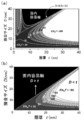
- (A) K i is 3 mJ / m 2 showing the calculation result of the thermal stability index (E / k B T) with respect to the junction size D and the layer thickness t of the ferromagnetic layer constituting the recording layer of the magnetoresistive element.
- graph assuming a graph on the assumption that 0 mJ / m 2 and (b) K i.
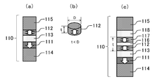
- 1A is a longitudinal sectional view showing a magnetoresistive effect element according to an embodiment of the present invention
- FIG. 2B is a perspective view of a second magnetic layer
- FIG. 2C is a perspective view of a second magnetic layer having different joint sizes at both end faces. It is.
- FIG. 1 It is a circuit diagram which shows the magnetic memory cell of the magnetic memory which has the conventional magnetoresistive effect element.
- FIG. 1 A) Longitudinal sectional view showing a conventional perpendicular magnetic anisotropic magnetoresistive effect element,
- the first magnetic layer 11 has a cylindrical shape, the magnetization direction is invariant upward or downward along the thickness direction, and is configured to function as a reference layer.
- the first magnetic layer 11 is made of a material containing at least one 3d ferromagnetic transition metal element such as Co, Fe, Ni, or Mn.
- the magnetoresistive effect element 10 one having a junction size D of 10 nm (D ⁇ 0.9t + 13 and D ⁇ t) and 40 nm (D> 0.9t + 13 and D> t) are produced.
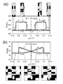
- the experiment was conducted by sweeping with a magnetic field of ⁇ 0.75 T.
- the element resistance was measured by a direct current four-terminal method with an applied voltage of 10 mV.
- the direction of sweeping with a perpendicular magnetic field ⁇ 0.75 T is indicated by an arrow.
- the magnetization directions of the first magnetic layer 11 and the second magnetic layer 12 are indicated by white arrows.
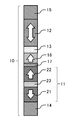
- the nonmagnetic layer 23 is made of a material containing any one of Ru, Rh, Ir, Cr, and Cu.
- the nonmagnetic layer 23 does not necessarily need to be made of such a material when the magnetization of the first magnetic layer 21 and the magnetization of the second magnetic layer 22 are antiparallel.
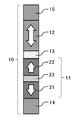
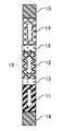
- the first magnetization layer 11 disposed between the first magnetic layer 11 and the first nonmagnetic layer 13 in the second modification example has an invariable magnetization direction. 3 magnetic layers 16, and a second nonmagnetic layer 17 disposed between the first magnetic layer 11 and the third magnetic layer 16.
- the third magnetic layer 16 has the same magnetization direction as the magnetization direction of the second magnetic layer 22 of the first magnetic layer 11.
- the third magnetic layer 16 is made of a material containing at least one 3d ferromagnetic transition metal element such as Co, Fe, Ni, or Mn.
- the second magnetic layer 12 is a composite recording in which a first magnetic layer 24, a nonmagnetic layer 25, and a second magnetic layer 26 are laminated in this order. Configured as a layer.
- the magnetization direction of the first magnetic layer 24 and the second magnetic layer 26 is variable up and down along the thickness direction.
- the first magnetic layer 24 and the second magnetic layer 26 are made of a material containing at least one 3d ferromagnetic transition metal element such as Co, Fe, Ni, or Mn.
- the third nonmagnetic layer 18 and the first magnetic layer 11 are magnetized in the opposite direction to the magnetization of the first magnetic layer 11 on the second magnetic layer 12.
- 4 magnetic layers 19 are laminated.
- the third nonmagnetic layer 18 is made of a compound containing oxygen such as MgO, Al 2 O 3 , SiO 2 , TiO, and Hf 2 O, and has a film thickness difference with respect to the first nonmagnetic layer 13. Yes.
- the third nonmagnetic layer 18 may be made of Cu, Ag, Au, or the like.
- the fourth magnetic layer 19 is made of a material containing at least one 3d ferromagnetic transition metal element such as Co, Fe, Ni, or Mn.
- the fourth magnetic layer 19 has a coercive force difference with respect to the first magnetic layer 11.
- FIG. 10 shows a seventh modification of the magnetoresistance effect element 10 according to the embodiment of the present invention.
- the seventh modification shown in FIG. 10 has the following configuration in order to reduce the current required for writing in the recording layer.
- the seventh modified example as shown in FIG. 10B, when D ⁇ 0.9t 1 +13 and D> 0.9t 3 +13, and the temperature T is T C1 ⁇ T C3 >T> T C2
- the intermediate magnetic layer 34 becomes paramagnetic, and the upper magnetic layer 35 becomes an in-plane magnetization polarization layer whose magnetization is in-plane, and works to assist the magnetization reversal of the lower magnetic layer 33. Can be done with current.
- the insulating layer 41 that covers the side surface of the second magnetic layer 12 that is a recording layer, the outside of the insulating layer 41, and the side surface of the second magnetic layer 12
- Electric field applying means 42 provided so that an electric field can be applied.
- the electric field applying means 42 applies an electric field to the recording layer. , Electric field induced magnetization reversal can be promoted.
- the sense amplifier 7 When reading, the sense amplifier 7 is used to read the signal difference due to resistance change.
- the sense amplifier 7 By using such a memory array, it is possible to realize an MRAM including the magnetoresistive effect element 10 having a large magnetoresistance change rate, a small write current, and higher thermal stability than the conventional structure.
Landscapes
- Engineering & Computer Science (AREA)
- Computer Hardware Design (AREA)
- Hall/Mr Elements (AREA)
- Mram Or Spin Memory Techniques (AREA)
Abstract
Description

D>t のとき、(Nz‐Nx)>0
D<t のとき、(Nz‐Nx)<0
すなわち、本発明に係る磁気抵抗効果素子は、磁化方向が不変である第1の磁性層と、磁化方向が可変である第2の磁性層と、前記第1の磁性層および前記第2の磁性層の厚さ方向に沿って、前記第1の磁性層と前記第2の磁性層との間に配置された第1の非磁性層とを備える磁気抵抗効果素子において、前記第1の磁性層および前記第2の磁性層の少なくともいずれか一方は、前記厚さ方向に垂直な端面上で最も長い直線の長さである接合サイズD(nm)と、層厚t(nm)との間に、D<0.9t+13 の関係を有していることを特徴とする。
図2は、本発明の実施の形態の磁気抵抗効果素子を示している。
図2(a)に示すように、磁気抵抗効果素子10は、第1の磁性層11と第2の磁性層12と第1の非磁性層13と下部非磁性電極14と上部非磁性電極15とを有している。
磁気抵抗効果素子10は、第2の磁性層12がD<0.9t+13 の関係を有しているため、形状磁気異方性により第2の磁性層12の磁化が垂直に向くように助長され、熱安定性を高めることができる。また、磁気抵抗効果素子10は、D<0.9t+13 とした熱安定性が高い状態で、接合サイズDをできる限り小さくすることにより、ビット情報を書込むときの書込み電流を小さくすることができる。第2の磁性層12の接合サイズDが30nm以下であるため、熱安定性指数70以上の熱安定性を得ることができる。
図3は、本発明の実施の形態の磁気抵抗効果素子10の、第1の変形例を示している。
図3に示す第1の変形例では、大きな磁気抵抗変化率を得るために、以下の構成を有している。
Ta(5)/Pt(5)/[Co(0.3)/Pt(0.4)]×20
/Co(0.3)/Ta(0.4)/Co20Fe60B20(1)
/MgO(1.0)/Co20Fe60B20(20)/Ta(1)/Ru(5)
/Ta(50)
[小括弧内は層厚(単位:nm)である]
ここで、[Co(0.3)/Pt(0.4)]×20/Co(0.3)が第1の磁性層11、Ta(0.4)が第2の非磁性層17、Co20Fe60B20(1)が第3の磁性層16、MgO(1.0)が第1の非磁性層13、Co20Fe60B20(20)が第2の磁性層12に対応している。第2の磁性層12の層厚tは、20nmである。
図5は、本発明の実施の形態の磁気抵抗効果素子10の、第2の変形例を示している。
この第2の変形例では、図5に示すように、第1の磁性層11は、第1の磁性層21と第2の磁性層22と非磁性層23とから構成されている。第1の磁性層11は、磁化が厚さ方向に沿って互いに反平行になるよう、第1の磁性層21および第2の磁性層22が非磁性層23を介して結合された反平行結合積層構造を有している。
図6は、本発明の実施の形態の磁気抵抗効果素子10の、第3の変形例を示している。図6に示す第3の変形例では、第2の変形例と比べて大きな磁気抵抗変化率を得るために、以下の構成を有している。
基板/Ta(5)/Pt(5)/[Co(0.3)/Pt(0.4)]x6
/Co(0.3)/Ru(0.4)
/[Co(0.3)/Pt(0.4)]x2/Co(0.3)
/Ta(0.4)/Co20Fe60B20(1)/MgO(1.0)
/Co20Fe60B20(20)/Ta(1)/Ru(5)/Ta(50)
[小括弧内は層厚(単位:nm)である]
ここで、[Co(0.3)/Pt(0.4)]x6/Co(0.3)が第1の磁性層11の第1の磁性層21、Ru(0.4)が非磁性層23、[Co(0.3)/Pt(0.4)]x2/Co(0.3)が第2の磁性層22、Ta(0.4)が第2の非磁性層17、Co20Fe60B20(1)が第3の磁性層16、MgO(1.0)が第1の非磁性層13、Co20Fe60B20(20)が第2の磁性層12に対応している。実験の結果、図4と同様の垂直磁化容易軸を反映した素子抵抗-磁界曲線が得られた。
また、これらの構造において、磁界パルスによる磁化反転確率から見積った結果、第2の磁性層12の層厚tと接合サイズDとの関係を、D<0.9t+13 とすることにより、熱安定性指数が70以上になることもわかった。
図7は、本発明の実施の形態の磁気抵抗効果素子10の、第4の変形例を示している。図7に示す第4の変形例では、第3の変形例よりもさらに大きな磁気抵抗変化率を得るために、以下の構成を有している。
図8は、本発明の実施の形態の磁気抵抗効果素子10の、第5の変形例を示している。図8に示す第5の変形例では、記録層の書込みに要する電流を低減するために、以下の構成を有している。
図9は、本発明の実施の形態の磁気抵抗効果素子10の、第6の変形例を示している。図9に示す第6の変形例では、記録層の書込みに要する電流を低減するために、以下の構成を有している。
図10は、本発明の実施の形態の磁気抵抗効果素子10の、第7の変形例を示している。図10に示す第7の変形例では、記録層の書込みに要する電流を低減するために、以下の構成を有している。
図11および図12は、本発明の実施の形態の磁気抵抗効果素子10の、第8の変形例を示している。
スピン注入磁化反転方式よりも電界誘起磁化反転方式の方が書込みの低消費電力化を図ることができると期待されているため、第8の変形例では、電界誘起磁化反転方式の構成を有している。
図13は、本発明の実施の形態の磁気メモリ(MRAM)を示している。
図13に示すように、磁気メモリ1は、それぞれ複数から成るソース線2とワード線3とビット線4とメモリセル5とを有している。
「1」の書込み動作では、ライトドライバ6からソース線2に電圧を印加するとともに、ワードドライバ8からワード線3に電圧を印加することによって、ソース線2から磁気抵抗効果素子10を介してビット線4に電流を流す。このとき、磁気抵抗効果素子10の磁化方向が可変の記録層である第2の磁性層12の磁化方向と、磁化方向が固定された参照層である第1の磁性層11の磁化方向とが反平行状態となる。これにより、磁気抵抗効果素子10は高抵抗状態となり、磁気抵抗効果素子10の保持する情報は「1」となる。
2 ソース線
3 ワード線
4 ビット線
5 メモリセル
6 ライトドライバ
7 センス増幅器
8 ワードドライバ
9 選択トランジスタ
10 磁気抵抗効果素子
11 第1の磁性層
21 第1の磁性層
22 第2の磁性層
23 非磁性層
12 第2の磁性層
24 第1の磁性層
25 非磁性層
26 第2の磁性層
31 下部磁性層
32 上部磁性層
33 下部磁性層
34 中間磁性層
35 上部磁性層
13 第1の非磁性層
14 下部非磁性電極
15 上部非磁性電極
16 第3の磁性層
17 第2の非磁性層
18 第3の非磁性層
19 第4の磁性層
41 絶縁層
42 電界印加手段
Claims (9)
- 磁化方向が不変である第1の磁性層と、磁化方向が可変である第2の磁性層と、前記第1の磁性層および前記第2の磁性層の厚さ方向に沿って、前記第1の磁性層と前記第2の磁性層との間に配置された第1の非磁性層とを備える磁気抵抗効果素子において、
前記第1の磁性層および前記第2の磁性層の少なくともいずれか一方は、前記厚さ方向に垂直な端面上で最も長い直線の長さである接合サイズD(nm)と、層厚t(nm)との間に、
D<0.9t+13
の関係を有していることを特徴とする磁気抵抗効果素子。 - 前記第1の磁性層および前記第2の磁性層の少なくともいずれか一方は、D<tの関係を有していることを特徴とする請求項1記載の磁気抵抗効果素子。
- D<0.9t+13の関係を有する前記第1の磁性層および/または前記第2の磁性層は、前記接合サイズが30nm以下であることを特徴とする請求項1記載の磁気抵抗効果素子。
- D<tの関係を有する前記第1の磁性層および/または前記第2の磁性層は、前記接合サイズが30nm以下であることを特徴とする請求項2記載の磁気抵抗効果素子。
- 前記第1の磁性層は、磁化が互いに反平行になるよう、2つの磁性層が非磁性層を介して結合された反平行結合積層構造を有していることを特徴とする請求項1乃至4のいずれか1項に記載の磁気抵抗効果素子。
- 前記第1の磁性層と前記第1の非磁性層との間に配置された、磁化方向が不変である第3の磁性層と、
前記第1の磁性層と前記第3の磁性層との間に配置された第2の非磁性層とを、
有することを特徴とする請求項1乃至5のいずれか1項に記載の磁気抵抗効果素子。 - 前記第2の磁性層は、互いに異なる材料から成る複数の磁性層を有することを特徴とする請求項1乃至6のいずれか1項に記載の磁気抵抗効果素子。
- 前記第2の磁性層の前記厚さ方向に沿った側面に電界を印加可能に設けられた電界印加手段を有することを特徴とする請求項1乃至7のいずれか1項に記載の磁気抵抗効果素子。
- 互いに平行に配置された複数のソース線と、
前記ソース線と交差する方向に、互いに平行に配置された複数のワード線と、
前記ソース線に平行に配置された複数のビット線と、
ゲート電極が前記ワード線に電気的に接続され、ソース電極が前記ソース線に電気的に接続された選択トランジスタと、
前記ビット線と前記ワード線とが交差する部分に配置され、前記第1の磁性層および前記第2の磁性層のいずれか一方が前記選択トランジスタのドレイン電極に電気的に接続され、他方が前記ビット線に電気的に接続された請求項1乃至8のいずれか1項に記載の磁気抵抗効果素子とを備え、
前記厚さ方向に沿って前記磁気抵抗効果素子に電流を印加可能に構成されていることを
特徴とする磁気メモリ。
Priority Applications (2)
| Application Number | Priority Date | Filing Date | Title |
|---|---|---|---|
| JP2015543838A JP6385355B2 (ja) | 2013-10-22 | 2014-10-20 | 磁気抵抗効果素子および磁気メモリ |
| US15/029,860 US9577182B2 (en) | 2013-10-22 | 2014-10-20 | Magnetoresistance effect element and magnetic memory |
Applications Claiming Priority (2)
| Application Number | Priority Date | Filing Date | Title |
|---|---|---|---|
| JP2013-219675 | 2013-10-22 | ||
| JP2013219675 | 2013-10-22 |
Publications (1)
| Publication Number | Publication Date |
|---|---|
| WO2015060239A1 true WO2015060239A1 (ja) | 2015-04-30 |
Family
ID=52992835
Family Applications (1)
| Application Number | Title | Priority Date | Filing Date |
|---|---|---|---|
| PCT/JP2014/077816 Ceased WO2015060239A1 (ja) | 2013-10-22 | 2014-10-20 | 磁気抵抗効果素子および磁気メモリ |
Country Status (4)
| Country | Link |
|---|---|
| US (1) | US9577182B2 (ja) |
| JP (1) | JP6385355B2 (ja) |
| TW (1) | TWI621120B (ja) |
| WO (1) | WO2015060239A1 (ja) |
Cited By (3)
| Publication number | Priority date | Publication date | Assignee | Title |
|---|---|---|---|---|
| KR20190062137A (ko) * | 2017-11-27 | 2019-06-05 | 삼성전자주식회사 | 자기 터널 접합 소자 및 자기저항 메모리 장치 |
| WO2019187800A1 (ja) * | 2018-03-30 | 2019-10-03 | 国立大学法人東北大学 | 磁気抵抗効果素子及び磁気メモリ |
| JP2022043545A (ja) * | 2020-09-04 | 2022-03-16 | Tdk株式会社 | 磁気抵抗効果素子および磁気メモリ |
Families Citing this family (9)
| Publication number | Priority date | Publication date | Assignee | Title |
|---|---|---|---|---|
| JP2017139399A (ja) * | 2016-02-05 | 2017-08-10 | Tdk株式会社 | 磁気メモリ |
| US10439133B2 (en) * | 2017-03-13 | 2019-10-08 | Samsung Electronics Co., Ltd. | Method and system for providing a magnetic junction having a low damping hybrid free layer |
| JP7024204B2 (ja) * | 2017-04-21 | 2022-02-24 | Tdk株式会社 | スピン流磁化回転素子、磁気抵抗効果素子及び磁気メモリ |
| FR3078443B1 (fr) | 2018-02-23 | 2023-01-13 | Commissariat Energie Atomique | Jonction tunnel magnetique a anisotropie de forme perpendiculaire et variabilite minimisee, point memoire et element logique comprenant la jonction tunnel magnetique, procede de fabrication de la jonction tunnel magnetique |
| US10878870B2 (en) * | 2018-09-28 | 2020-12-29 | Spin Memory, Inc. | Defect propagation structure and mechanism for magnetic memory |
| JP2020155460A (ja) * | 2019-03-18 | 2020-09-24 | キオクシア株式会社 | 磁気記憶装置 |
| JP2021145025A (ja) | 2020-03-11 | 2021-09-24 | キオクシア株式会社 | 磁気記憶装置及び磁気記憶装置の製造方法 |
| US11710707B2 (en) * | 2020-03-26 | 2023-07-25 | Shibaura Mechatronics Corporation | Electromagnetic wave attenuator, electronic device, film formation apparatus, and film formation method |
| JP7383576B2 (ja) * | 2020-07-01 | 2023-11-20 | 株式会社東芝 | 磁気ヘッド及び磁気記録装置 |
Citations (3)
| Publication number | Priority date | Publication date | Assignee | Title |
|---|---|---|---|---|
| JP2001196661A (ja) * | 1999-10-27 | 2001-07-19 | Sony Corp | 磁化制御方法、情報記憶方法、磁気機能素子および情報記憶素子 |
| WO2009107780A1 (ja) * | 2008-02-28 | 2009-09-03 | 日本電気株式会社 | 磁気抵抗記憶装置及びその動作方法 |
| JP2012195485A (ja) * | 2011-03-17 | 2012-10-11 | Toshiba Corp | 磁気記録素子及び不揮発性記憶装置 |
Family Cites Families (7)
| Publication number | Priority date | Publication date | Assignee | Title |
|---|---|---|---|---|
| JP4040173B2 (ja) | 1998-06-05 | 2008-01-30 | キヤノン株式会社 | メモリ |
| JP4253225B2 (ja) * | 2003-07-09 | 2009-04-08 | 株式会社東芝 | 磁気抵抗効果素子および磁気メモリ |
| JP5542831B2 (ja) * | 2009-09-24 | 2014-07-09 | 株式会社東芝 | 磁気メモリ |
| JP5725735B2 (ja) | 2010-06-04 | 2015-05-27 | 株式会社日立製作所 | 磁気抵抗効果素子及び磁気メモリ |
| JP2013140891A (ja) * | 2012-01-05 | 2013-07-18 | Toshiba Corp | 磁気抵抗効果素子の製造方法 |
| JP2013197215A (ja) * | 2012-03-16 | 2013-09-30 | Toshiba Corp | 磁気記憶装置 |
| JP5490167B2 (ja) * | 2012-03-23 | 2014-05-14 | 株式会社東芝 | 磁気メモリ |
-
2014
- 2014-10-20 JP JP2015543838A patent/JP6385355B2/ja active Active
- 2014-10-20 WO PCT/JP2014/077816 patent/WO2015060239A1/ja not_active Ceased
- 2014-10-20 US US15/029,860 patent/US9577182B2/en active Active
- 2014-10-22 TW TW103136451A patent/TWI621120B/zh active
Patent Citations (3)
| Publication number | Priority date | Publication date | Assignee | Title |
|---|---|---|---|---|
| JP2001196661A (ja) * | 1999-10-27 | 2001-07-19 | Sony Corp | 磁化制御方法、情報記憶方法、磁気機能素子および情報記憶素子 |
| WO2009107780A1 (ja) * | 2008-02-28 | 2009-09-03 | 日本電気株式会社 | 磁気抵抗記憶装置及びその動作方法 |
| JP2012195485A (ja) * | 2011-03-17 | 2012-10-11 | Toshiba Corp | 磁気記録素子及び不揮発性記憶装置 |
Cited By (9)
| Publication number | Priority date | Publication date | Assignee | Title |
|---|---|---|---|---|
| KR20190062137A (ko) * | 2017-11-27 | 2019-06-05 | 삼성전자주식회사 | 자기 터널 접합 소자 및 자기저항 메모리 장치 |
| JP2019096815A (ja) * | 2017-11-27 | 2019-06-20 | 株式会社サムスン日本研究所 | 磁気トンネル接合素子及び磁気抵抗メモリ装置 |
| KR102534061B1 (ko) * | 2017-11-27 | 2023-05-18 | 삼성전자주식회사 | 자기 터널 접합 소자 및 자기저항 메모리 장치 |
| WO2019187800A1 (ja) * | 2018-03-30 | 2019-10-03 | 国立大学法人東北大学 | 磁気抵抗効果素子及び磁気メモリ |
| JPWO2019187800A1 (ja) * | 2018-03-30 | 2021-06-17 | 国立大学法人東北大学 | 磁気抵抗効果素子及び磁気メモリ |
| JP7258363B2 (ja) | 2018-03-30 | 2023-04-17 | 国立大学法人東北大学 | 磁気抵抗効果素子及び磁気メモリ |
| US11770981B2 (en) | 2018-03-30 | 2023-09-26 | Tohoku University | Magnetoresistive element and magnetic memory |
| JP2022043545A (ja) * | 2020-09-04 | 2022-03-16 | Tdk株式会社 | 磁気抵抗効果素子および磁気メモリ |
| JP7520651B2 (ja) | 2020-09-04 | 2024-07-23 | Tdk株式会社 | 磁気抵抗効果素子および磁気メモリ |
Also Published As
| Publication number | Publication date |
|---|---|
| TW201528265A (zh) | 2015-07-16 |
| JPWO2015060239A1 (ja) | 2017-03-09 |
| JP6385355B2 (ja) | 2018-09-12 |
| US9577182B2 (en) | 2017-02-21 |
| TWI621120B (zh) | 2018-04-11 |
| US20160233416A1 (en) | 2016-08-11 |
Similar Documents
| Publication | Publication Date | Title |
|---|---|---|
| JP6385355B2 (ja) | 磁気抵抗効果素子および磁気メモリ | |
| JP6948706B2 (ja) | 磁気抵抗効果素子および磁気メモリ | |
| JP5867030B2 (ja) | 記憶素子、記憶装置 | |
| KR102024410B1 (ko) | 자기저항 효과 소자 및 자기 메모리 | |
| JP5600344B2 (ja) | 磁気抵抗効果素子及び磁気メモリ | |
| JP4874884B2 (ja) | 磁気記録素子及び磁気記録装置 | |
| JP6194752B2 (ja) | 記憶素子、記憶装置、磁気ヘッド | |
| JP5987613B2 (ja) | 記憶素子、記憶装置、磁気ヘッド | |
| CN102800803A (zh) | 存储元件和存储设备 | |
| JP7169683B2 (ja) | 磁気抵抗効果素子及び磁気メモリ | |
| JP2015002281A (ja) | 記憶素子、記憶装置、記憶素子の製造方法、磁気ヘッド | |
| JP2014072393A (ja) | 記憶素子、記憶装置、磁気ヘッド | |
| JP2013115319A (ja) | 記憶素子、記憶装置 | |
| JP2010098259A (ja) | メモリセル、ならびに、磁気メモリ素子 | |
| TWI422083B (zh) | Magnetic memory lattice and magnetic random access memory | |
| CN103137854A (zh) | 存储元件和存储装置 | |
| JP2012069958A (ja) | 磁気記録素子 | |
| KR20110098899A (ko) | 자기 메모리 소자 및 불휘발성 기억장치 | |
| JP7258363B2 (ja) | 磁気抵抗効果素子及び磁気メモリ | |
| WO2020026637A1 (ja) | 磁気抵抗効果素子及び磁気メモリ | |
| JP2017212464A (ja) | 記憶素子、記憶装置、磁気ヘッド | |
| JP5777124B6 (ja) | 磁気抵抗効果素子、磁性膜、及び、磁性膜の製造方法 |
Legal Events
| Date | Code | Title | Description |
|---|---|---|---|
| ENP | Entry into the national phase |
Ref document number: 2015543838 Country of ref document: JP Kind code of ref document: A |
|
| WWE | Wipo information: entry into national phase |
Ref document number: 15029860 Country of ref document: US |
|
| NENP | Non-entry into the national phase |
Ref country code: DE |
|
| 121 | Ep: the epo has been informed by wipo that ep was designated in this application |
Ref document number: 14854919 Country of ref document: EP Kind code of ref document: A1 |
|
| 122 | Ep: pct application non-entry in european phase |
Ref document number: 14854919 Country of ref document: EP Kind code of ref document: A1 |