WO2015045779A1 - 力学量測定装置及びその製造方法 - Google Patents
力学量測定装置及びその製造方法 Download PDFInfo
- Publication number
- WO2015045779A1 WO2015045779A1 PCT/JP2014/073293 JP2014073293W WO2015045779A1 WO 2015045779 A1 WO2015045779 A1 WO 2015045779A1 JP 2014073293 W JP2014073293 W JP 2014073293W WO 2015045779 A1 WO2015045779 A1 WO 2015045779A1
- Authority
- WO
- WIPO (PCT)
- Prior art keywords
- sensor chip
- solder
- layer
- base substrate
- mechanical quantity
- Prior art date
- Legal status (The legal status is an assumption and is not a legal conclusion. Google has not performed a legal analysis and makes no representation as to the accuracy of the status listed.)
- Ceased
Links
Images





Classifications
-
- G—PHYSICS
- G01—MEASURING; TESTING
- G01L—MEASURING FORCE, STRESS, TORQUE, WORK, MECHANICAL POWER, MECHANICAL EFFICIENCY, OR FLUID PRESSURE
- G01L9/00—Measuring steady of quasi-steady pressure of fluid or fluent solid material by electric or magnetic pressure-sensitive elements; Transmitting or indicating the displacement of mechanical pressure-sensitive elements, used to measure the steady or quasi-steady pressure of a fluid or fluent solid material, by electric or magnetic means
- G01L9/0041—Transmitting or indicating the displacement of flexible diaphragms
-
- G—PHYSICS
- G01—MEASURING; TESTING
- G01L—MEASURING FORCE, STRESS, TORQUE, WORK, MECHANICAL POWER, MECHANICAL EFFICIENCY, OR FLUID PRESSURE
- G01L19/00—Details of, or accessories for, apparatus for measuring steady or quasi-steady pressure of a fluent medium insofar as such details or accessories are not special to particular types of pressure gauges
- G01L19/0092—Pressure sensor associated with other sensors, e.g. for measuring acceleration or temperature
-
- G—PHYSICS
- G01—MEASURING; TESTING
- G01L—MEASURING FORCE, STRESS, TORQUE, WORK, MECHANICAL POWER, MECHANICAL EFFICIENCY, OR FLUID PRESSURE
- G01L9/00—Measuring steady of quasi-steady pressure of fluid or fluent solid material by electric or magnetic pressure-sensitive elements; Transmitting or indicating the displacement of mechanical pressure-sensitive elements, used to measure the steady or quasi-steady pressure of a fluid or fluent solid material, by electric or magnetic means
- G01L9/0041—Transmitting or indicating the displacement of flexible diaphragms
- G01L9/0051—Transmitting or indicating the displacement of flexible diaphragms using variations in ohmic resistance
- G01L9/0052—Transmitting or indicating the displacement of flexible diaphragms using variations in ohmic resistance of piezoresistive elements
- G01L9/0054—Transmitting or indicating the displacement of flexible diaphragms using variations in ohmic resistance of piezoresistive elements integral with a semiconducting diaphragm
-
- H—ELECTRICITY
- H10—SEMICONDUCTOR DEVICES; ELECTRIC SOLID-STATE DEVICES NOT OTHERWISE PROVIDED FOR
- H10W—GENERIC PACKAGES, INTERCONNECTIONS, CONNECTORS OR OTHER CONSTRUCTIONAL DETAILS OF DEVICES COVERED BY CLASS H10
- H10W72/00—Interconnections or connectors in packages
- H10W72/071—Connecting or disconnecting
- H10W72/073—Connecting or disconnecting of die-attach connectors
-
- H—ELECTRICITY
- H10—SEMICONDUCTOR DEVICES; ELECTRIC SOLID-STATE DEVICES NOT OTHERWISE PROVIDED FOR
- H10W—GENERIC PACKAGES, INTERCONNECTIONS, CONNECTORS OR OTHER CONSTRUCTIONAL DETAILS OF DEVICES COVERED BY CLASS H10
- H10W72/00—Interconnections or connectors in packages
- H10W72/071—Connecting or disconnecting
- H10W72/075—Connecting or disconnecting of bond wires
-
- H—ELECTRICITY
- H10—SEMICONDUCTOR DEVICES; ELECTRIC SOLID-STATE DEVICES NOT OTHERWISE PROVIDED FOR
- H10W—GENERIC PACKAGES, INTERCONNECTIONS, CONNECTORS OR OTHER CONSTRUCTIONAL DETAILS OF DEVICES COVERED BY CLASS H10
- H10W72/00—Interconnections or connectors in packages
- H10W72/851—Dispositions of multiple connectors or interconnections
- H10W72/874—On different surfaces
- H10W72/884—Die-attach connectors and bond wires
Definitions
- the present invention relates to a mounting structure of a mechanical quantity measuring device and a manufacturing method thereof.
- strain gauge As a method for measuring the deformation (strain) of a measurement object, a technique using a metal foil strain gauge utilizing the fact that the resistance value of the metal foil changes due to the strain is known. By attaching this strain gauge to the object to be measured, the length of the metal foil is changed following the strain of the object to be measured, and the resistance value of the metal foil that changes as a result can be detected to enable strain measurement of the object to be measured.
- Technology Up to now, there are strain gauges using Cu-Ni alloy foils and Ni-Cr alloy foils, etc. In addition to ensuring and stabilizing strain gauge attachment (sticking), it is also moisture and impact resistant. High protector strain gauges have also been proposed.
- Patent Document 2 has a strain detection element formed of a silicon chip and a pedestal that transmits strain to be detected to the strain detection element.
- the pedestal has a thermal expansion coefficient of ⁇ 50% of the thermal expansion coefficient of silicon.
- a strain detection sensor is disclosed in which a silicon chip formed of a material that falls within the range, a glass-based fixing material heated and melted, and a strain detection element formed on the pedestal is fixed.
- a semiconductor strain gauge As a semiconductor strain gauge, accuracy and sensitivity for accurately transmitting strain generated in a measured object to a strain detection unit of a semiconductor chip (hereinafter referred to as a sensor chip) are important. In addition, when the same amount of distortion occurs in the object to be measured for a long time, the stability of the sensor output value indicating the same detection value is important in the sensor chip. These requirements become a difficult problem when the object to be measured is used at a high temperature. In addition to general household items, applications for measuring mechanical quantities such as strain and pressure can be used for controlling the operation of automobile devices and monitoring important infrastructures, for example. In this case, it is necessary to assume the usage environment up to a temperature range of about 150 ° C. at high temperatures.
- the main material of the sensor chip is silicon, and it is bonded to the object to be measured using a bonding material such as solder.
- This bonding needs to be performed at a temperature lower than the heat resistance temperature of the sensor chip.
- solder As a general solder, Sn-3 wt% Ag-0.5 wt% Cu solder having a melting point of about 217 ° C., Pb-5 wt% Sn solder having a melting point of about 310 ° C. are known. With Sn-3wt% Ag-0.5wt% Cu solder, the temperature is close to the melting point in the operating environment near 100 ° C to 150 ° C, and the yield stress of the solder becomes small and softens.
- Patent Document 1 filed so far uses an organic thin film, so it is predicted that it is difficult to use at high temperatures. Further, Patent Document 2 shows a structure in which a glass-based fixing material is used by being heated and melted, and can be expected to be a hard material. It is considered necessary.
- the performance of the sensor is greatly influenced by the structure of the joint between the sensor chip and the object to be measured.
- strain detection part in a semiconductor substrate, and a to-be-measured object is optimized, and the distortion which generate
- the present application includes a plurality of means for solving the above problems.
- an initial metallized layer including a material that forms a solid solution with Au and forms a solid solution strengthening is formed on a base substrate, and at least 50 wt% or more of Au is included on the initial metallized layer.
- a sensor chip in which a solder is stacked, a sensor chip in which a strain detection portion is formed on a semiconductor substrate is mounted on the solder with the back surface thereof facing, and the stacked body is placed in a heating furnace, so that the heat resistance of the sensor chip is increased.
- a bonding layer is formed by heating at a temperature below the solder melting temperature or higher and melting part or all of the material for solid solution strengthening of Au in the solder from the initial metallized layer in contact with the solder into the solder. I did it. Furthermore, a wiring board for drawing out wiring from the electrode of the sensor chip to the outside is attached and configured.
- a material that forms a solid solution with Au on the surface of a member constituting a mechanically measured object and includes a material that solidifies and strengthens Au is included.
- An initial metallization layer is formed, a solder containing at least 50 wt% or more of Au is laminated on the initial metallization layer of the member, and a sensor chip having a strain detection portion formed on a semiconductor substrate is formed on the solder, and a back surface thereof is formed.
- the laminated body is placed in the heating furnace, heated to a temperature lower than the heat resistance temperature of the sensor chip and higher than a solder melting temperature, and Au in the solder is fixed from the initial metallized layer in contact with the solder.
- a part or all of the material to be melt strengthened is dissolved in solder to form a bonding layer on the surface of the member constituting the object to be measured, and the sensor chip and the member constituting the object to be measured are directly bonded.
- the present invention provides a method for manufacturing a mechanical quantity measuring device, characterized in that a wiring board for drawing wiring from the electrode of the sensor chip to the outside is attached.
- a mechanical quantity measuring device is interposed between a sensor chip in which a strain detection unit is formed on a semiconductor substrate, and an object to be measured and the sensor chip. And a base substrate that transmits the strain of the measurement object to be detected to the sensor chip, and a wiring portion that draws wiring from the electrode of the sensor chip to the outside, the base substrate, the sensor chip,
- a solid solution containing Au and the material is formed by melting a material that solidifies and strengthens Au from the metallized layer to be connected.
- a bonding layer made of solder, and a metallized layer having the remaining material dissolved into the solder layer to which the material is connected, the base substrate, the sensor chip, Are configured to be joined.
- a member constituting an object to be measured of the mechanical quantity is provided, and between the member and the sensor chip. Has a laminated metallized layer and a bonding layer, and the sensor chip is directly bonded to the member.
- a high-performance mechanical quantity measuring device and a manufacturing process thereof can be provided.
- a mechanical quantity measuring device that can reduce chip cracking failure during joining of the sensor chip and the object to be measured, and that can be manufactured at a high yield, and a manufacturing process thereof.
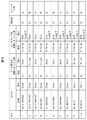
- the mechanical quantity measuring apparatus of Example 1 of the present invention the results of verifying the effect of preventing chip cracking at the time of joining and improving the creep resistance at high temperature by using a combination of various metallized layers and solder. It is a summarized table. It is a figure explaining the process which joins a sensor chip and a base substrate within a heating furnace in the manufacturing method of the mechanical quantity measuring device of Example 2 of this invention. It is an example of the cross-sectional block diagram of the mechanical quantity measuring apparatus of Example 2 of this invention. It is a figure explaining the process which joins a sensor chip and a base substrate in a heating furnace in the manufacturing method of the mechanical quantity measuring device of Example 3 of this invention.
- a mechanical quantity measuring device is provided as a product
- the base substrate is mounted when the user attaches (attaches / connects) the mechanical quantity measuring device to the object to be measured and measures the distortion generated in the object to be measured.
- This is a connection element for facilitating connection to the object to be measured.
- the sensor chip 1 has a strain detection portion 2 on the main surface 1a, and the sensor chip back surface 1b, which is the surface opposite to the main surface 1a of the sensor chip 1, has a bonding layer 3, a metallized layer 5, and an intermediate metallized layer 6 interposed therebetween. And connected to the base substrate 4.
- the strain detector 2 is provided near the center of the sensor chip, and a Wheatstone bridge circuit composed of four impurity diffusion resistors is formed. As a result, the strain is detected by the resistance value of the impurity diffusion resistor changing due to the expansion and contraction generated in the plane direction of the sensor chip 1.
- the sensor chip 1 is provided with a part for measuring temperature as required. If the temperature can be measured at the same time, the temperature of the measured value can be corrected, and a more accurate strain amount can be measured.
- the sensor chip 1 is disposed at substantially the center of the base substrate 4, but there is no problem even if it is not particularly the center.
- a printed circuit board 20 is disposed on the base substrate 4, and the electrode pads 21 on the printed circuit board 20 and the electrode pads 29 of the sensor chip 1 are connected by bonding wires 22 using Au wire or the like.
- the printed board 20 may be a board using a glass epoxy material, a flexible board using a polyimide material, or a ceramic board. Further, wiring may be created in the base substrate 4 in accordance with a method for producing a metal base substrate, and the base substrate 4 and the printed circuit board 20 may be combined into one.
- a metallized layer 5 is disposed on the base substrate 4 at the mounting position of the sensor chip 1, and the bonding layer 3 between the metallized layer 5 and the sensor chip 1 is a solder layer containing Au, and Si, Ge, Ni, Sn, It is configured to include one or more elements of In and Sb and one or more elements of Cu, Ag, Co, Pt, Cr, Fe, and Pd.
- the metallized layer 5 on the base substrate 4 contains one or more elements of Cu, Ag, Co, Pt, Cr, Fe, and Pd.
- An intermediate metallized layer 6 such as Ni may be provided between the base substrate 4 and the metallized layer 5 in order to improve the adhesion of the metallized layer 5.
- the metallized layer is generally used in such a manner that it is sandwiched between the solder layer and the material to be joined in order to improve the wettability between the solder layer and the material to be joined and improve the adhesion.
- the metallized layer contains an element that dissolves into the solder layer and forms a solid solution with Au contained in the solder layer or an intermetallic compound to modify the Au phase, and joins the element. It also has a role of supplying to the department.
- FIG. 3 is a diagram illustrating a process for joining the sensor chip 1 and the base substrate 4 in the heating furnace 10 in the method for manufacturing the mechanical quantity measuring device 100. That is, an intermediate metallized layer 6 and an initial metallized layer 7 are disposed on the base substrate 4, a solder material 8 containing Au is mounted on the initial metallized layer 7, and then a main part having a strain detecting portion 2 of the sensor chip 1. The surface 1 b opposite to the surface 1 a is mounted so as to contact the solder material 8. On the back surface 1 b of the sensor chip 1, Ti, Ni, Au layer, Ti, Pt, Au layer, Ti, Pt, Ag layer, Ti, Ni as an initial metallization layer 9 in order to improve the bondability with the solder material 8.
- the Ag layer is applied by plating or vapor deposition. These are put in the heating furnace 10 and heated by, for example, a heater 11 or the like. As the heating and temperature rise, the solder material 8 containing Au melts and is bonded to the initial metallization layer 9 on the back surface 1 b of the sensor chip 1 and the initial metallization layer 7 of the base substrate 4. At this time, the initial metallization layer 7 of the base substrate 4 includes one or more elements of Cu, Ag, Co, Pt, Cr, Fe, and Pd. Then, some or all of the components of the initial metallization layer are dissolved in the solder material 8 containing Au from the initial metallization layer 7 of the base substrate 4.
- the surface Au, Ag layer, etc. of the initial metallized layer 9 are generally thin and melt into the solder material 8 containing Au during connection, and the Ni layer (shown) Not).
- FIG. 4 shows the state of the bonding layer when the entire initial metallized layer 7 is dissolved in the solder containing Au.
- the intermediate metallized layer 6 and the solder come into contact with each other, and a part of the intermediate metallized layer 6 may be dissolved in the solder.
- An intermetallic compound layer 13 is formed at the interface.
- An intermetallic compound layer 14 is formed between the surface of the sensor chip 1 and the initial metallized layer 9.
- the intermediate bonding layer 15 has a composition in which the initial metallized layer 7 is dissolved in Au.
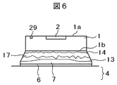
- FIG. 5 shows a state of the bonding layer when a part of the initial metallized layer 7 is dissolved in the solder material 8 containing Au. Since a part of the initial metallized layer 7 is melted, a part of the initial metallized layer 7 remains on the intermediate metallized layer 6, and the intermetallic compound layer 13 is formed adjacent thereto. Further, an intermetallic compound layer 14 is also formed between the surface of the sensor chip 1 and the initial metallized layer 9.
- the intermediate bonding layer 17 has a composition in which the components of the initial metallized layer 7 are dissolved in Au.
- the initial metallization layer 7 is not uniformly melted into the solder material 8 containing Au, and as shown in FIG.
- the melt around the chip is faster than the central part of the chip, and the initial metallization layer 7 near the center remains thick. There are many cases. Thus, only the lower part of the center part of the chip becomes the thick metallized layer 7, and the ratio of solder in the bonding layer 17 is small and the reliability is improved.
- the bonding layer 3 or the bonding layers 15 and 17 between the sensor chip 1 and the base substrate 4 after cooling generally soft Au is solid-solution strengthened by the dissolution of the components of the initial metallized layer 7.
- values such as hardness, tensile strength, and Young's modulus are increased, and the hard bonding layers 3, 15, and 17 can be formed.
- the bonding layers 3, 15, and 17 are hard layers, it is possible to transmit a change in mechanical quantity generated in the base substrate 4 to the strain detection unit 2 on the surface of the sensor chip 1 with high sensitivity. In addition, even in a long period, creep deformation in the bonding layer 3 is reduced, and the sensor output is stabilized.
- the joint structure is capable of high-sensitivity and long-term stable sensor measurement.
- each component of the initial metallization layer 7 is dissolved in the solder material 8 containing Au at the time of bonding. It becomes possible to form a reinforcing layer by modifying soft Au. As a result, the amount of creep deformation of the solder at a high temperature is reduced, and a high-sensitivity and stable sensor measurement can be performed for a long period of time. It is important to optimize the heating conditions because the rate of penetration into the solder material 8 containing Au varies depending on the components of the initial metallization layer 7. However, after joining, baking is performed again at a high temperature to promote diffusion. This process is also effective.
- N 2 or the like is effective as the atmosphere, but in addition to this, reducing hydrogen, a mixture thereof, or an organic acid such as formic acid may be used. In addition, an organic substance such as a flux capable of reducing the surface oxide may be used.
- a bonding correction jig 12 such as a weight 16 or a guide may be used. It is also effective to reduce the voids by vacuuming the periphery of these joining members.
- solder material 8 containing Au is supplied onto the initial metallized layer 7 of the base substrate 4, while the sensor chip 1 is vacuum-adsorbed with a collet or the like, and the sensor chip 1 is pressed onto the solder material 8. At this time, it is also possible to heat the collet in a pulsed manner (pulse heat) or constantly (constant heat) to melt the solder material 8 containing Au and join the sensor chip 1 and the base substrate 4 together. . If the base substrate is heated in advance, the bonding time can be further shortened.
- Al, Al alloy, Cu, Cu alloy, SUS, 42 alloy, Mo, CIC or the like can be used as the material of the base substrate 4.
- solder material containing Au, Au and Ge, Au and Si, Au and In, Au and Sn, Au and Sb binary solder, or Ge, Si, In, Sn, Ni, Sb, Ti, Cu, A solder composed of two or more types of Ag and the remainder composed of Au is suitable.
- the Au composition is desirably 50 wt% or more.
- the melting point is lowered to the eutectic temperature of about 363 ° C. by adding about 3.15 wt% Si as compared with Au having a melting point of 1063 ° C. It is possible to bond at a temperature of about 370 to 450 ° C., which is lower than the heat resistance of.
- the metallization component is dissolved in Au, the melting point of the bonding layers 3, 15, and 17 is increased, and the bonding layer is strengthened by the solid solution strengthening and creep. Resistance is improved.
- the melting point is lowered to about 356 ° C. of the eutectic temperature by adding about 12 wt% Ge as compared with Au having a melting point of 1063 ° C. Bonding is possible at a temperature of about 370 to 450 ° C, which is lower than heat resistance.
- the metallization component is dissolved in Au, the melting point of the bonding layers 3, 15, and 17 is increased, and the bonding layer is strengthened by the solid solution strengthening and creep. Resistance is improved.
- bonding is first performed by reducing the probability of chip cracking by bonding using AuGe eutectic containing 12wt% Ge in Au or a material having a low melting point in the vicinity thereof, and at the same time, metallizing.
- a process of improving the strength by modifying the soft Au phase using the penetration of the Au strengthening component from the layer is effective.
- the composition having the lowest melting point and the composition in the vicinity thereof are used to reduce the probability of chip cracking by bonding below the heat resistant temperature of the chip.
- a process of improving the strength by modifying the soft Au phase using the penetration of the Au reinforcing component from the metallized layer 7 is effective.
- the melting point of the solder material can be adjusted by using a solder material that contains two or more of Ge, Si, In, Sn, Ni, Sb, Ti, Cu, and Ag, and the remainder is made of Au. Therefore, high yield bonding can be performed in accordance with the heat resistance and chip cracking strength of the sensor chip. For example, in the case of a solder material containing Ge and Si in Au, the melting point is lowered to 350 ° C. or less depending on the composition, so that it is possible to reduce the incidence of chip crack failure during bonding.
- FIG. 7 shows a configuration diagram when measuring the strain amount of the device under test 30 using the mechanical quantity measuring apparatus 100 of the present invention.
- the base substrate 4 and the DUT 30 are fixed at several locations by welding 31.
- the amount of strain generated in the object to be measured 30 is first transmitted to the base substrate 4, and then transmitted to the strain detection unit 2 of the sensor chip 1 with high sensitivity via the bonding layer 3 with improved sensitivity and creep resistance. It becomes possible to accurately measure the amount of distortion.
- the base substrate 4 and the object to be measured are fixed by welding 31, but may be fixed by screwing, an adhesive, caulking, a method using heat due to friction, or the like.
- the surface including the surface of the sensor chip 1 and the bonding wire 22 is covered with an insulating material or the like in order to protect the surface of the sensor chip 1 of the mechanical quantity measuring apparatus 100 or the bonding wire 22. May be. Alternatively, it may be possible to cover the whole with a cap or the like.
- the sensor chip 1 has a size of approximately 1 mm to 5 mm square, a thickness of 50 to 400 ⁇ m, and the bonding layer 3 has a thickness of about 200 ⁇ m at the maximum.
- the base substrate 4 has a thickness of about 0.1 to 3 mm.
- the solder material 8 containing Au is a solder pellet having a size suitable for the size of each chip and a thickness of about 20 to 200 ⁇ m.
- the thickness of the initial metallized layer having a component that can be strengthened by modifying soft Au is, for example, about 100 ⁇ m at maximum, depending on the modification effect of the component.
- the base substrate 4 was made of SUS420, the thickness was 1 mm, Ni was applied as the intermediate metallized layer 6, and Cu was applied as the initial metallized layer 5. The thickness of each layer varies depending on manufacturing, but the intermediate metallized layer made of Ni was 3 ⁇ m, and the initial metallized layer made of Cu was 10 ⁇ m. These metallized layers were formed on the entire base substrate 4 by plating.
- a solder material 8 containing Au a binary material of Au-3.15 wt% Si was used, and a solder pellet having a shape approximately the same size as the chip and a thickness of 30 ⁇ m was prepared.
- the sensor chip 1 is 3 mm square, and Ti / Ni / Au is applied to the surface 1 b opposite to the strain detection unit 2.
- the base substrate 4, Au-3.15 wt% Si solder pellets, and sensor chip 1 were sequentially laminated, heated at a maximum temperature of 400 ° C. for about 3 minutes in a reflow furnace in an N 2 atmosphere, and then cooled.
- Cu is used as a component that can be modified and strengthened by soft Au
- Cu is dissolved in Au in the bonding layer 3, and the amount of penetration varies depending on the location. Almost 30 to 70 at% of Cu was dissolved.
- the region where the intermediate metallization layer 6 and the initial metallization layer 7 are formed on the base substrate 4 may be formed entirely, or the metallization layer may be formed only in the vicinity where the sensor chip 1 is mounted. . In this case, partial plating using a resist or the like is performed. Alternatively, the intermediate metallized layer 6 may be applied to the entire base substrate 4, and then the initial metallized layer 7 may be applied only to a portion where the sensor chip 1 is mounted by masking with a resist or the like.
- the material of the base substrate 4 is a material such as SUS that has a stable surface and poor adhesion to the plating and is likely to be peeled off
- the metallized layer with a small area may be concerned about characteristic deterioration due to peeling.
- Another effect of modifying such an Au-based solder is the concern with brittle materials because Au is very soft, but mainly modified by the effect of solid solution strengthening. This is effective when there is little problem of impact resistance, especially when reliability for vibration and impact is important, such as in automobile applications. In addition, it has high resistance at low temperatures and is excellent in reliability such as temperature cycle. Further, since Si and Au, which are the main materials of the sensor chip 1, cause a eutectic reaction, by optimizing the temperature and atmosphere, a part of the side surface of the sensor chip 1 or the side surface as shown in FIG. It is also possible to form the fillet 23 as a whole, and the creep resistance is improved.
- the sensor chip 1 is the same as that of the first embodiment, but the initial metallized layer containing a component that can be strengthened by modifying the soft Au of the solder material 8 containing Au. 41 is formed on the back surface 1 b of the sensor chip 1.
- FIG. 9 is a diagram showing a method for manufacturing the mechanical quantity measuring apparatus 200.
- the sensor chip 1 and the base substrate 4 are joined in the heating furnace 10, and a normal metallized layer 42 is formed on the base substrate 4.
- the solder material 8 containing Au is mounted on the metallized layer 42, and then the initial metallized layer 41 formed on the surface 1 b opposite to the main surface 1 a on which the strain detecting portion 2 of the sensor chip 1 is provided is the solder material 8. Mounted to touch. Thereafter, by heating, the components of the initial metallization layer 41 formed on the back surface 1b of the sensor chip 1 are dissolved in the solder material 8 containing Au, and the joining structure of the mechanical quantity measuring device 200 shown in FIG. 10 is formed. .
- the bonding layer 43 in this example is made of solder that is modified and strengthened by soft Au.
- the material of the initial metallization layer 41 is the same as that of the initial metallization layer 7 of the first embodiment.
- the solder material 8 is the same as that in the first embodiment.
- a part or all of the initial metallized layer 41 on the back surface 1b of the sensor chip 1 is melted into the solder 8 containing Au, and although not shown, an intermetallic compound layer or the like is formed at the interface. .
- an intermetallic compound layer or the like is formed at the interface. .
- the sensor chip 1 is the same as that of the first embodiment, but the initial metallized layer containing a component that can be strengthened by modifying the soft Au of the solder material 8 containing Au. Is formed on both the back surface 1 b of the sensor chip 1 and the base substrate 4.
- FIG. 11 is a diagram showing a method of manufacturing the mechanical quantity measuring device 300.
- the sensor chip 1 and the base substrate 4 are joined in the heating furnace 10, and an initial metallized layer 44 including a component capable of strengthening soft Au is formed on the base substrate 4.
- a solder material 8 containing Au is mounted on the metallized layer 44, and then the surface 1 b opposite to the main surface 1 a where the strain detection portion 2 of the sensor chip 1 is in contact with the solder material 8.
- an initial metallized layer 45 containing a component capable of reinforcing soft Au is formed on the back surface 1b of the sensor chip 1 in the same manner.
- an intermediate metallized layer 6 may be formed between the base substrate 4 and the initial metallized layer 44 for the purpose of improving adhesion.
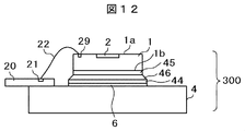
- solder material in which the components of the initial metallization layer 45 formed on the back surface 1b of the sensor chip 1 and the components of the initial metallization layer 44 formed on the surface of the base substrate 4 contain Au. 8 is formed to form the joint structure of the mechanical quantity measuring apparatus 300 shown in FIG.
- the bonding layer 46 in this example is made of solder which is reinforced by modifying soft Au. Specifically, a part or all of the initial metallization layer 45 on the back surface 1b of the sensor chip 1 and the initial metallization layer 44 of the base substrate 4 is melted into the solder 8 containing Au. An intermetallic compound layer or the like is formed.
- the initial metallization layer 45 on the back surface 1b of the sensor chip 1 and the initial metallization layer 44 of the base substrate are made of such materials and structures, thereby improving the creep resistance at high temperatures and improving the sensitivity of the object to be measured. It becomes possible to measure the mechanical quantity change. In addition, the probability of chip cracking during joining can be reduced.
- the initial metallization layer 45 of the sensor chip 1 and the initial metallization layer 44 on the surface of the base substrate 4 may be the same component, or different components may be used.
- the materials of the initial metallization layer 44 and the initial metallization layer 45 are the same as those of the initial metallization layer 7 of the first embodiment.
- the solder material 8 is the same as that in the first embodiment.
- Example 3 the initial metallized layers 44 and 45 containing a component capable of strengthening soft Au are formed on both the base substrate 4 and the back surface 1b of the sensor chip 1 to further dissolve into the solder material 8. An example of improving efficiency quickly was shown. In order to realize further rapid melting into the solder material 8, it is considered effective to sandwich an initial metallized layer between the solder materials 8.
- the sensor chip 1 is the same as that of the first embodiment, but the initial metallized layer containing a component that can be strengthened by modifying the soft Au of the solder material 8 containing Au. Is formed in three places on the back surface 1b of the sensor chip 1 and the base substrate 4 between the solder material 8 containing Au.
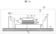
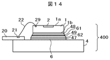
- FIG. 13 is a diagram showing a method for manufacturing the mechanical quantity measuring apparatus 400.
- the sensor chip 1 and the base substrate 4 are joined in the heating furnace 10, and an initial metallized layer 47 containing a component capable of strengthening soft Au is formed on the base substrate 4.
- a solder material 8 containing Au is mounted on the metallized layer 47, a sheet-like Au modified material 49 and a solder material 8 containing Au are mounted on the metallized layer 47, and then there is a strain detecting portion 2 of the sensor chip 1.
- the surface 1 b opposite to the main surface 1 a is mounted so as to contact the solder material 8.
- an initial metallized layer 48 including a component capable of reinforcing soft Au is formed on the back surface 1b of the sensor chip 1 in the same manner.
- an intermediate metallized layer 6 may be formed between the base substrate 4 and the initial metallized layer 47 for the purpose of improving adhesion.
- the joining layers 61 and 62 in this example are made of solder which is reinforced by modifying soft Au. Specifically, the initial metallization layer 48 on the back surface 1 b of the sensor chip 1, the Au modified material 49 sandwiched between the solder materials 8, and a solder in which part or all of the initial metallization layer 47 on the base substrate 4 contains Au.
- the intermetallic compound layer and the like are formed at the interface.
- the initial metallization layer 48 on the back surface 1b of the sensor chip 1, the Au modified material 49 sandwiched between the solder materials 8, and the initial metallization layer 47 on the base substrate are adopted. It is possible to improve creep resistance at high temperature and measure the mechanical quantity change of the measurement object with high sensitivity. In addition, the probability of chip cracking during joining can be reduced.
- the initial metallized layer 48 of the sensor chip 1, the Au modified material 49 sandwiched between the solder materials 8, and the initial metallized layer 47 on the surface of the base substrate 4 may be the same component, Ingredients may be used.
- the materials of the initial metallization layer 48, the Au modifying material 49, and the initial metallization layer 47 are the same as those of the initial metallization layer 7 of the first embodiment.
- the solder material 8 is the same as that in the first embodiment.
- either or both of the initial metallized layers 47 and 48 formed on the base substrate 4 or the back surface 1b of the sensor chip 1 are omitted, and the Au modification is performed only between the solder materials 8.
- a configuration in which the bonding material is formed by sandwiching the material 49 is also conceivable.
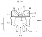
- FIG. 15 An example in which the mechanical quantity measuring device of the present invention is applied to a pressure sensor module is shown in FIG.
- a pressure sensor module 500 whose sectional view is shown in FIG. 15 has a container 54 including a cylindrical portion 52 provided with a hollow hole 51 inside and a lid portion 53 for closing the upper portion of the hollow hole 51 in the cylindrical portion 52.
- a region of a diaphragm 56 is formed in the lid portion 53 at the upper portion of the hollow hole 51
- the sensor module 57 in which the sensor chip 1 is attached to the base substrate 4 via the bonding layer 3 is the hollow hole 51 in the diaphragm 56 portion. It is attached to the opposite side.
- a wiring board 20 is attached via a bonding wire 22. Further, a case 58 and a connector (not shown) are attached around the sensor module (mechanical quantity measuring device) 57 for protecting the sensor module 57 and outputting the measurement value.
- the base substrate 4 is made of, for example, a CIC substrate, Mo, 42 Alloy, SUS, Al, ceramic, or the like, and the cylindrical portion 52, the diaphragm 56, or the like is made of, for example, SUS material.
- the case 58 is made of resin or the like, but may be made of a metal material if it does not have heat resistance.
- the joining of the diaphragm 56 and the base substrate 4 is performed using welding, brazing material, screw fixing, caulking, heat due to friction, or the like. Further, when the volume of the pressure sensor module 500 is limited and cannot be stored, the printed board 20 uses a flexible board or a springy thing such as a connector or a probe pin to extract a signal. It is also possible.
- the joint portion 55 is connected to, for example, a hydraulic piping of an automobile. Therefore, the sensor chip 1 connected to the base substrate 4 bonded to the diaphragm 56 via the bonding layer described in the first to fourth embodiments of the present invention is distorted through the diaphragm 56 according to the change in hydraulic pressure. Convert pressure changes into electrical signals.
- a sensor module (mechanical quantity measuring device) 57 in which the sensor chip 1 is attached to the base substrate 4 via the bonding layer 3 may be separately prepared and then attached to the lid portion 53.
- the process of attaching the sensor chip 1 after attaching the base substrate 4 to the lid portion 53 first may be used.
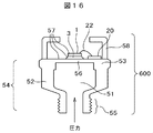
- a pressure sensor module 600 structure in which the sensor chip 1 is directly bonded to the diaphragm 56 (measurement target) without using the base substrate 4 is also possible.
- This example (modification) is shown in FIG. 16, in which the sensor chip 1 is directly bonded to the diaphragm 56 using the bonding layer described in the first to fourth embodiments of the present invention, and the diaphragm 56 is distorted according to the change in hydraulic pressure. By detecting this amount of strain by the strain detector 2 of the sensor chip 1, the change in pressure is converted into an electrical signal.
- the pressure sensor modules 500 and 600 created in this way even when the joint part 3 of the sensor chip 1 is high temperature, the creep deformation is small and stable, and the reliability such as the temperature cycle is high.
- the pressure change when used in a high-temperature environment can be measured with high sensitivity and stably for a long period of time.
- there are few chip cracking defects and the yield is good.
Landscapes
- Physics & Mathematics (AREA)
- General Physics & Mathematics (AREA)
- Chemical & Material Sciences (AREA)
- Analytical Chemistry (AREA)
- Measurement Of Length, Angles, Or The Like Using Electric Or Magnetic Means (AREA)
- Pressure Sensors (AREA)
- Die Bonding (AREA)
- Measuring Fluid Pressure (AREA)
Abstract
半導体基板にひずみ検出部を有するセンサチップとベース基板との接合部を最適化し、被測定物に生じたひずみを高温下でも高感度に検出し、且つ、長期間ひずみが負荷された場合でもクリープ変形が少なく、安定したセンサ出力が可能な接合構造を提案する。ベース基板上に、Auと固溶体を形成してAuを固溶強化する材料を含む初期メタライズ層を形成し、初期メタライズ層上にAuを含むはんだを積層し、はんだの上に、センサチップを、その裏面を向けて搭載し、前記積層体を加熱炉内に載置して、センサチップの耐熱温度以下、及びはんだ溶融温度以上に加熱し、前記初期メタライズ層からはんだ中のAuを固溶強化する前記材料の一部、或いは全部をはんだ中に溶解させて接合層を形成することを特徴とする力学量測定装置の製造方法を提案する。
Description
本発明は力学量測定装置の実装構造、及びその製造方法に関する。
測定対象の変形(ひずみ)を測定する方法として、金属箔の抵抗値がひずみによって変化することを利用した金属箔ひずみゲージを用いる技術が知られている。このひずみゲージを測定対象に接着することで測定対象のひずみに追従して金属箔の長さを変化させ、その結果変化する金属箔の抵抗値を検出することにより測定対象のひずみ測定を可能にする技術である。これまでに、Cu-Ni系合金箔やNi-Cr系合金箔などを用いたひずみゲージがあり、また、ひずみゲージ添着(貼付け)の確実、安定化を図るとともに、防湿性、耐衝撃性の高いプロテクタ付きひずみゲージも提案されている。
しかしながら、これらは消費電力が大きいため、電池がすぐに消費してしまう問題があった。そこで、低消費電力化するために、シリコンにひずみ感応抵抗体を形成した半導体歪ゲージが提案されている。
この半導体歪ゲージを従来の金属薄膜を用いた歪みゲージの代わりに被計測対象に貼り付ける構造としては、複数の電極が設けられた可橈性薄膜と、複数の電気素子が形成された半導体基板とを有し、上記可橈性薄膜は、上記半導体基板に被着されていて、上記複数の電極と上記複数の電気素子とは電気的に接続されていることを特徴とする半導体歪ゲージの構造が、特許文献1に提案されている。
また、特許文献2には、シリコンチップで構成される歪み検出素子と、検出すべき歪みを歪み検出素子に伝える台座を有し、台座は熱膨張係数がシリコンの熱膨張係数の±50%の範囲に入る材料で形成され、ガラス系固定材を加熱溶融して前記台座に歪み検出素子が形成されたシリコンチップを固定した歪み検出センサが開示されている。
半導体歪ゲージとしては、被測定物に生じた歪みを、半導体チップ(以下センサチップと呼ぶ)の歪み検出部に正しく伝える精度、感度が重要である。また、被測定物に同じ量の歪みが長時間生じている場合には、センサチップでは同じ検出値を示すセンサ出力値の安定性が重要である。これらの要求は、被測定物が高温で使用される場合には、難しい課題となる。歪みや圧力などの力学量測定の用途としては、一般的な家庭用品のほかに、例えば、自動車の各機器の動作制御や、重要なインフラの監視などに用いられることも考えられる。この場合の使用環境は、高温では150℃程度の温度範囲までも想定する必要がある。
通常センサチップの主な材質はシリコンであり、被測定物とは、はんだなどの接合材料を用いて接合される。この接合はセンサチップの耐熱温度以下で行う必要がある。一般的なはんだとしては、融点が217℃付近のSn-3wt%Ag-0.5wt%Cuはんだや、融点が約310℃のPb-5wt%Snはんだなどが知られる。Sn-3wt%Ag-0.5wt%Cuはんだでは、100℃~150℃付近の使用環境では融点に近い温度となり、はんだの降伏応力が小さくなり軟化するため、感度低下が懸念されるとともに、高温でひずみが負荷され続けるような条件では接合層のクリープなどの変形が起き、センサ出力の変動が問題となる。鉛を多く含むPb-5wt%Snはんだなどは、Sn系はんだと比較して融点は高いが、柔らかい材料であるため、感度低下、センサ出力値の変動がやはり懸念される。
そこで、高温でのセンサの正常な動作を確保するために、非常に高融点の硬い接合材料を用いてセンサチップと被測定物とを接合することも考えられるが、接合温度はセンサチップの耐熱温度を超えることはできない。また、高温で接合する場合にはセンサチップと被測定物との熱膨張係数差により、接合時にシリコンチップに割れが生じる場合があり、製造時の歩留まり低下も懸念される。
これまで出願されている特許文献1では有機薄膜を用いているため、高温での使用は難しいと予測される。また、特許文献2では、ガラス系固定材を加熱溶融して用いる構造が示されていて硬い材料であると期待できるが、衝撃などの外力によって破壊されることも懸念され、使用環境の制約も必要と考えられる。
このように、半導体歪ゲージの実装構造においては、センサチップと被測定物の接合部の構造によって、感度やセンサ出力安定性などのセンサとして重要な性能が大きく影響される。このため、本発明では、半導体基板にひずみ検出部を有するセンサチップと被測定物との接合部を最適化し、被測定物に生じたひずみを高温下でも高感度に、且つ、正確に検出することが可能なセンサチップの接合構造(センサチップ、その接合部構造を含めて本発明では以下力学量測定装置と呼ぶ)、及びその製造方法を提供することを目的とする。
また、センサチップと被測定物の接合時のチップ割れ不良を防ぎ、高歩留まりで製造可能なセンサチップ接合構造、及びその製造方法を提供することも目的とする。
本願は上記課題を解決する手段を複数含んでいるが、その一例を挙げるならば、
力学量測定装置の製造方法において、ベース基板上に、Auと固溶体を形成してAuを固溶強化する材料を含む初期メタライズ層を形成し、前記初期メタライズ層上にAuを少なくとも50wt%以上含むはんだを積層し、前記はんだの上に、半導体基板にひずみ検出部を形成したセンサチップを、その裏面を向けて搭載し、前記積層体を加熱炉内に載置して、前記センサチップの耐熱温度以下、及びはんだ溶融温度以上に加熱し、前記はんだに接する前記初期メタライズ層からはんだ中のAuを固溶強化する前記材料の一部、或いは全部をはんだ中に溶解させて接合層を形成するようにした。更に、前記センサチップの電極から外部に配線を引き出す配線基板を取り付けて構成するようにした。
力学量測定装置の製造方法において、ベース基板上に、Auと固溶体を形成してAuを固溶強化する材料を含む初期メタライズ層を形成し、前記初期メタライズ層上にAuを少なくとも50wt%以上含むはんだを積層し、前記はんだの上に、半導体基板にひずみ検出部を形成したセンサチップを、その裏面を向けて搭載し、前記積層体を加熱炉内に載置して、前記センサチップの耐熱温度以下、及びはんだ溶融温度以上に加熱し、前記はんだに接する前記初期メタライズ層からはんだ中のAuを固溶強化する前記材料の一部、或いは全部をはんだ中に溶解させて接合層を形成するようにした。更に、前記センサチップの電極から外部に配線を引き出す配線基板を取り付けて構成するようにした。
また、上記課題を解決するために本発明では、前記ベース基板に代えて、力学量の被測定物を構成する部材の表面に、Auと固溶体を形成してAuを固溶強化する材料を含む初期メタライズ層を形成し、前記部材の初期メタライズ層上に、Auを少なくとも50wt%以上含むはんだを積層し、前記はんだの上に、半導体基板にひずみ検出部を形成したセンサチップを、その裏面を向けて搭載し、前記積層体を前記加熱炉内に載置し、前記センサチップの耐熱温度以下、及びはんだ溶融温度以上に加熱し、前記はんだに接する前記初期メタライズ層からはんだ中のAuを固溶強化する前記材料の一部、或いは全部をはんだ中に溶解させて被測定物を構成する部材の表面に接合層を形成し、前記センサチップと、被測定物を構成する部材とを直接接合する方法を提供する。更に、前記センサチップの電極から外部に配線を引き出す配線基板を取り付けて構成することを特徴とする力学量測定装置の製造方法を提供する。
また、上記課題を解決するために本発明では、力学量測定装置を、半導体基板にひずみ検出部を形成したセンサチップと、被測定物と前記センサチップとの間に介在して、前記センサチップを支持すると共に、検出すべき前記被測定物の歪みを前記センサチップに伝えるベース基板と、前記センサチップの電極から外部に配線を引き出す配線部とを備え、前記ベース基板と、前記センサチップとの間には、加熱前にはAuを少なくとも50wt%以上含み、加熱炉内の加熱によって、接続する前記メタライズ層からAuを固溶強化する材料の溶け込みにより、Auと前記材料を含む固溶体を形成するはんだから成る接合層と、前記材料が接続するはんだ層へ溶け出した残りの材料を有するメタライズ層とを有して、前記ベース基板と、前記センサチップとが接合されているように構成した。
また、上記課題を解決するために本発明では、前記力学量測定装置において、前記ベース基板に代えて、力学量の被測定物を構成する部材を備え、前記部材と、前記センサチップとの間には、積層状の前記メタライズ層と前記接合層とを有して、前記センサチップを直接、前記部材へ接合して構成した。
本発明によれば、被測定物に生じたひずみを高温下でも高感度に検出し、且つ、長期間ひずみが負荷された場合でも、安定して正確なセンサ出力が可能な接合構造となり、高性能な力学量測定装置、及びその製造プロセスを提供することができる。
また、センサチップと被測定物との接合時のチップ割れ不良を低減することができ、高歩留まりで製造することが可能な力学量測定装置、及びその製造プロセスを提供することができる。
以下、本発明の実施例について、図面を用いて説明する。ただし、以下の説明において、同一構成要素には同一符号を付し繰り返しの説明を省略することがある。なお、図面は説明をより明確にするため、実際の態様に比べ、各部の幅、厚さ、形状等について模式的に表される場合があるが、あくまで一例であって、本発明の解釈を限定するものではない。本発明は下記の実施例に限定されるものではなく、種々変更可能であることはいうまでもない。
本実施例では、力学量測定装置の構成部品であるセンサチップとベース基板とそれらの接合部の構造の例を説明する。ベース基板は、力学量測定装置を製品として提供する場合に、ユーザが被測定対象に力学量測定装置を取り付けて(貼り付け・接続して)、被測定対象に生じた歪みを計測する際に、被測定対象への接続を容易にするための接続要素となるものである。なお、ベース基板を用いずに、センサチップを被測定対象を構成する部材に直接接合する力学量測定装置の構成方法も以下の実施例に説明する。
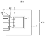
図1、図2は、本実施例の力学量測定装置100の断面構造と平面構造の例を示す図である。センサチップ1は、主面1aにひずみ検出部2を有し、センサチップ1の主面1aの反対の面であるセンサチップ裏面1bは接合層3、メタライズ層5、および中間メタライズ層6を介して、ベース基板4に接続されている。ひずみ検出部2はセンサチップの中央付近に設けられていて、4つの不純物拡散抵抗からなるホイートストンブリッジ回路が形成されている。これにより、センサチップ1の平面方向に生じた伸縮によって不純物拡散抵抗の抵抗値が変化することによりひずみを検出する。またこのセンサチップ1には、必要に応じて温度を測定する部位を形成しておく。このように温度計測が同時にできれば計測値の温度補正が可能となり、より高精度なひずみ量が計測可能となる。この例ではセンサチップ1は、ベース基板4のほぼ中央部に配置されているが、特に中央部でなくても問題はない。
ベース基板4上には、プリント基板20が配置され、プリント基板20上の電極パッド21とセンサチップ1の電極パッド29とがAu線などを用いたボンディングワイヤ22により接続される。プリント基板20はガラスエポキシ材料を用いた基板でも良いし、ポリイミド材料などを用いたフレキシブルな基板、セラミック基板などでも良い。また、メタルベース基板の作成方法に従ってベース基板4に配線も作り込み、ベース基板4とプリント基板20を1つにしても良い。
ベース基板4にはセンサチップ1の搭載位置にメタライズ層5が配置され、メタライズ層5とセンサチップ1の間の接合層3は、Auを含むはんだ層であり、Si、Ge、Ni、Sn、In、Sbのうち1種類以上の元素と、Cu、Ag、Co、Pt、Cr、Fe、Pdのうち1種類以上の元素を含んで構成されている。ベース基板4上のメタライズ層5は、Cu、Ag、Co、Pt、Cr、Fe、Pdのうち1種類以上の元素を含むものである。ベース基板4とメタライズ層5の中間は、メタライズ層5の密着性を向上させるために、Niなどの中間メタライズ層6を設けても良い。
ベース基板4にはセンサチップ1の搭載位置にメタライズ層5が配置され、メタライズ層5とセンサチップ1の間の接合層3は、Auを含むはんだ層であり、Si、Ge、Ni、Sn、In、Sbのうち1種類以上の元素と、Cu、Ag、Co、Pt、Cr、Fe、Pdのうち1種類以上の元素を含んで構成されている。ベース基板4上のメタライズ層5は、Cu、Ag、Co、Pt、Cr、Fe、Pdのうち1種類以上の元素を含むものである。ベース基板4とメタライズ層5の中間は、メタライズ層5の密着性を向上させるために、Niなどの中間メタライズ層6を設けても良い。
メタライズ層は、通常はんだ層と被接合材との濡れ性を高めて密着性を向上するためにはんだ層と被接合材との間に挟んで接合されるなどの使用法が一般的である。本発明の実施例では、メタライズ層は、はんだ層へ溶け込んで、はんだ層に含まれるAuと固溶体、または金属間化合物を形成してAu相を改質する元素を含んでいて、該元素を接合部へ供給する役割も持つところが特徴である。
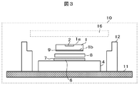
図3に、力学量測定装置100の製造方法において、加熱炉10内でセンサチップ1とベース基板4とを接合するプロセスを説明する図を示す。すなわちベース基板4上には中間メタライズ層6と初期メタライズ層7が配置され、この初期メタライズ層7上にAuを含むはんだ材料8が搭載され、次にセンサチップ1のひずみ検出部2のある主面1aと反対の面1bがはんだ材料8に接するように搭載されている。センサチップ1の裏面1bには、はんだ材料8との接合性を向上させるために初期メタライズ層9としてTi、Ni、Au層、Ti、Pt、Au層、Ti、Pt、Ag層、Ti、Ni、Ag層などをめっき、あるいは蒸着により施されている。これらを加熱炉10内に入れ、例えばヒータ11などによって加熱する。
加熱、昇温と共に、Auを含むはんだ材料8が溶融し、センサチップ1の裏面1bの初期メタライズ層9、及びベース基板4の初期メタライズ層7に接合される。このとき、ベース基板4の初期メタライズ層7は、Cu、Ag、Co、Pt、Cr、Fe、Pdのうち1種類以上の元素を含むものとする。すると、ベース基板4の初期メタライズ層7から、これらの初期メタライズ層の成分の一部、或いは全部がAuを含むはんだ材料8内に溶解する。
加熱、昇温と共に、Auを含むはんだ材料8が溶融し、センサチップ1の裏面1bの初期メタライズ層9、及びベース基板4の初期メタライズ層7に接合される。このとき、ベース基板4の初期メタライズ層7は、Cu、Ag、Co、Pt、Cr、Fe、Pdのうち1種類以上の元素を含むものとする。すると、ベース基板4の初期メタライズ層7から、これらの初期メタライズ層の成分の一部、或いは全部がAuを含むはんだ材料8内に溶解する。
一方、センサチップ1の界面では、初期メタライズ層9の表層のAu、Ag層などは一般的に薄く接続中にAuを含むはんだ材料8中に溶け込み、その下に形成したNi層(図示していない)などと接合されることとなる。
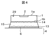
Auを含むはんだ中に初期メタライズ層7の全部が溶け込んだ場合の接合層の様子を図4に示す。初期メタライズ層7の全てがAuを含むはんだ材料8に溶け込むと、中間メタライズ層6とはんだが接して、中間メタライズ層6の一部がはんだ中に溶けこむ場合があるが、中間メタライズ層6との界面に金属間化合物層13が形成される。またセンサチップ1表面の初期メタライズ層9との間に金属間化合物層14が形成される。その中間の接合層15は、Au中に初期メタライズ層7が溶け込んだ組成となっている。
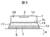
図5に、初期メタライズ層7の一部がAuを含むはんだ材料8に溶け込んだ場合の接合層の様子を示す。初期メタライズ層7の一部が溶け込むため、中間メタライズ層6上に初期メタライズ層7の一部が残り、これに隣接して金属間化合物層13が形成される。またセンサチップ1表面の初期メタライズ層9との間にも金属間化合物層14が形成される。これらの中間の接合層17はAu中に初期メタライズ層7の成分が溶け込んだ組成となっている。Auを含むはんだ材料8への初期メタライズ層7の溶け込みは均一ではなく、図6に示したように、チップ周囲の溶け込みがチップ中央部に比べて速く、中央付近の初期メタライズ層7が厚く残ることが多い。このように、チップ中央部の下部のみ厚いメタライズ層7となり、接合層17中のはんだの割合が少なく信頼性が向上する。
以上のように、冷却後のセンサチップ1とベース基板4間の接合層3、或いは接合層15、17においては、一般的に軟質なAuが初期メタライズ層7の成分の溶け込みによって固溶強化される。このため、硬度、引張り強度、ヤング率などの値が大きくなり、硬い接合層3、15、17を形成することが可能である。このように接合層3、15、17が硬い層となるため、ベース基板4に生じる力学量変化をセンサチップ1表面の歪み検出部2に感度良く伝達することが可能となる。また、長期間においても接合層3内のクリープ変形が低減し、センサ出力が安定する。
例えば、初期メタライズ層7にAgを用いた場合には、接合時、Auを含むはんだ材料8にAgが溶け込み、Au中に固溶する。AuとAgは全率固溶する関係であり、溶解速さも早く、製造上問題とならない。したがって、冷却後の接合層3、15、17のAuは、初期のはんだ材料8のAuとは異なりAgが固溶したものとなっていて、固溶強化により軟質なAuが改質し強化層が形成されることとなる。且つ、Agが溶け込むことにより接合層3、15、17の融点も上昇させることが可能となることから、高温でのはんだのクリープ変形量を低減できる。したがって、高感度で、且つ長期間安定したセンサ計測が可能な接合構造となる。
他には、初期メタライズ層7にCuを用いた場合には、接合時、Auを含むはんだ材料8にCuが溶け込み、Au中に固溶する。したがって、冷却後の接合層3、15、17のAuは、初期のはんだ材料8のAuとは異なりCuが固溶したものとなり、固溶強化により軟質なAuが改質され強化層が形成されることとなる。しかも、AuとCuの場合にはCu含有量によってAuCuの規則格子が形成され、軟質なAuを大幅に強化させる効果がある。この場合には、接合後、高温で長時間ベークし、規則格子化を促進するプロセスの追加が有効である。且つ、Au中にCuが溶解することにより接合層の融点も上昇し、高温でのはんだのクリープ変形量が低減し、高感度で、且つ、長期間安定したセンサ計測が可能な接合構造となる。
他には、初期メタライズ層7にPt、Ni、Co、Cr、Fe、Pd層を用いた場合にも同様に、接合時、Auを含むはんだ材料8に初期メタライズ層7の各成分が溶け込み、軟質なAuを改質して強化層を形成することが可能となる。これにより、高温でのはんだのクリープ変形量が低減し、高感度で、且つ、長期間安定したセンサ計測が可能な接合構造となる。
初期メタライズ層7の成分によってAuを含むはんだ材料8への溶け込み速さは異なるため、加熱条件を最適化することが重要であるが、接合後、再度高温でのベーク処理を行い、拡散を進行させるプロセスも有効である。
初期メタライズ層7の成分によってAuを含むはんだ材料8への溶け込み速さは異なるため、加熱条件を最適化することが重要であるが、接合後、再度高温でのベーク処理を行い、拡散を進行させるプロセスも有効である。
ここで、加熱炉10の内部は雰囲気制御を行うことで、Auを含むはんだ材料8の表面酸化を抑制し、良好な接合を得ることができる。例えば、雰囲気はN2などが有効であるが、このほかに、還元性のある水素、あるいはこれらの混合物、または、ギ酸などの有機酸を用いても良い。他には、表面酸化物を還元可能なフラックスなどの有機物を用いても良い。センサチップ1の平行性、所望の接合高さ確保、位置ずれ防止、接合層中のボイド低減を図るために重り16やガイドなどの接合補正冶具12を用いても良い。またこれらの接合部材周辺を真空にしてボイドを低減させることも効果的である。このような工夫を行うことで、ボイドなどの欠陥の少ない良好な接合層3、15、17を得ることが可能になる。更に接合性を向上させるには、接合前のスパッタ処理や、プラズマ洗浄などを行い、接合部材の有機汚染量、酸化膜などを除去、或いは低減させておくことが有効である。
また加熱炉だけではなく、いわゆるダイボンダ装置を用いることも可能である。ベース基板4の初期メタライズ層7上にAuを含むはんだ材料8を供給し、一方、センサチップ1をコレットなどで真空吸着させて、センサチップ1をはんだ材料8上に圧着する。このとき、コレットをパルス的に加熱(パルスヒート)、或いはコンスタントに加熱して(コンスタントヒート)、Auを含むはんだ材料8を溶融させてセンサチップ1とベース基板4を接合させることも可能である。ベース基板は予め加熱しておくと、より接合時間が短縮化できる。このダイボンド接合時でも、接合部付近を不活性雰囲気にしておくと、より良好な接合が可能となる。このダイボンドによる接合後に、高温槽などの他の装置などに移して再度加熱し、メタライズ層7成分の接合層17への溶解量を増やすことも可能である。
ベース基板4の材料としては、Al、Al合金、Cu、Cu合金、SUS、42アロイ、Mo、CICなどを用いることができる。
Auを含むはんだ材料としては、AuとGe、AuとSi、AuとIn、AuとSn、AuとSbの2元はんだ、或いは、Ge、Si、In、Sn、Ni、Sb、Ti、Cu、Agのうち2種類以上を含み残りがAuで構成されるはんだが適当である。Auの組成は50wt%以上が望ましい。
例えば、AuとSiを含む2元系はんだでは、融点が1063℃のAuと比較して、約3.15wt%のSiの添加により融点が共晶温度の363℃程度まで下降するため、センサチップ1の耐熱性以下の約370~450℃付近の温度で接合することが可能である。しかし、上記構成の初期メタライズ層7と接合することにより、Au中にメタライズ成分が固溶して接合層3、15、17の融点は上昇し、且つ固溶強化により接合層は強化され、クリープ耐性が向上する。初めから、Au、Si、及び初期メタライズ層からの溶け込み成分を含んだ高融点で、且つ高強度の接合材料を用いて接合することも考えられるが、センサチップ1の耐熱性、接合時のチップ割れ発生も考慮すると、製造上の課題が多い。そこで、まずはAuに3.15wt%のSiを含むAuSi共晶、或いはその付近の融点の低い組成のはんだ材料を用いて接合することによりチップ割れ発生確率を低減して確実に接合を行い、と同時に、メタライズ層からのAu強化成分の溶け込みを利用して軟質なAu相の改質を行い高強度化するプロセスが有効である。
同様にAuとGeを含む2元系はんだでは、融点が1063℃のAuと比較して、約12wt%のGeの添加により融点が共晶温度の356℃程度まで下降するため、センサチップ1の耐熱性以下の約370~450℃付近の温度で接合することが可能である。しかし、上記構成の初期メタライズ層7と接合することにより、Au中にメタライズ成分が固溶して接合層3、15、17の融点は上昇し、且つ固溶強化により接合層は強化され、クリープ耐性が向上する。初めからAu、Ge、及び初期メタライズ層からの溶け込み成分を含んだこのような高融点で、且つ高強度の接合材料を用いて接合することも考えられるが、センサチップの耐熱性、接合時のチップ割れ発生も考慮すると、製造上の課題が多い。そこで、まずはAuに12wt%のGeを含むAuGe共晶、或いはその付近の融点の低い組成の材料を用いて接合することによりチップ割れ発生確率を低減して確実に接合を行い、と同時に、メタライズ層からのAu強化成分の溶け込みを利用して軟質なAu相の改質を行い高強度化するプロセスが有効である。
他にも、AuSn、AuIn、AuNi、AuSb系では、最も融点の低くなる組成、及びその付近の組成を用いて、チップの耐熱温度以下で接合してチップ割れ発生確率を低減し、且つ、初期メタライズ層7からのAu強化成分の溶け込みを利用して軟質なAu相の改質を行い高強度化するプロセスが有効である。
或いは、Ge、Si、In、Sn、Ni、Sb、Ti、Cu、Agのうち2種類以上を含み残りがAuで構成されるはんだ材料を用いることにより、はんだ材料の融点を調整することが可能であるため、センサチップの耐熱性、チップ割れ強度に合わせて高歩留まりの接合を行うことが可能である。例えば、Au中にGeとSiを含むはんだ材料では、組成によって融点が350℃以下まで低下するため、接合時のチップ割れ不良発生率を低くすることが可能である。
またこのように少しでも低融点のはんだ材料を用いて接合することにより、製造時の電力などを低減でき、環境負荷も低減することが可能である。
図7に本発明の力学量測定装置100を利用して被測定物30のひずみ量を計測する場合の構成図を示す。これはベース基板4と被測定物30とを、溶接31によって数箇所固定したものである。これにより、被測定物30に生じたひずみ量をまずはベース基板4に伝え、その後、感度、クリープ耐性を向上させた接合層3を介してセンサチップ1の歪み検出部2に、感度良く伝え、歪み量を正確に測定することが可能となる。ここでは、溶接31によりベース基板4と被測定物を固定したが、ねじ留めや接着材、かしめ、摩擦による熱を利用する方法などで固定しても良い。
図7に本発明の力学量測定装置100を利用して被測定物30のひずみ量を計測する場合の構成図を示す。これはベース基板4と被測定物30とを、溶接31によって数箇所固定したものである。これにより、被測定物30に生じたひずみ量をまずはベース基板4に伝え、その後、感度、クリープ耐性を向上させた接合層3を介してセンサチップ1の歪み検出部2に、感度良く伝え、歪み量を正確に測定することが可能となる。ここでは、溶接31によりベース基板4と被測定物を固定したが、ねじ留めや接着材、かしめ、摩擦による熱を利用する方法などで固定しても良い。
また、図示していないが、これらの力学量測定装置100のセンサチップ1の表面保護、或いはボンディングワイヤ22などの保護のため、センサチップ1表面とボンディングワイヤ22を含むエリアを絶縁材料などで覆ってもよい。または、キャップなどで全体を覆うことも考えられる。
次に本実施例の力学量測定装置100の形状について説明する。例えば、センサチップ1はほぼ1mm~5mm角、厚さは50~400μmのサイズであり、接合層3の厚さは最大200μm程度のサイズである。ベース基板4は0.1~3mm程度の厚さであるが、ベース基板を用いず被測定物に直接接合する場合には、更に厚いものでも問題ない。またAuを含むはんだ材料8は、それぞれのチップの大きさに適する大きさで、厚みは20~200μm程度のはんだペレットを用いる。しかしこれ以外にも、円盤状のはんだペレット、ボール形状のはんだ、線状のはんだ、或いははんだ粒子を有機物と混合させたはんだペーストを用いても良い。
また軟質なAuを改質して強化できる成分を有する初期メタライズ層の厚みは、その成分の改質効果にもよるが、例えば最大100μm程度である。
また軟質なAuを改質して強化できる成分を有する初期メタライズ層の厚みは、その成分の改質効果にもよるが、例えば最大100μm程度である。
一例として、AuとSiの2元はんだを用いた例を示す。ベース基板4にはSUS420を用い、厚みを1mmとし、これに中間メタライズ層6としてNiを施し、これに初期メタライズ層5としてCuを施した。それぞれの層の厚みは、製造上のばらつきもあるが、Niによる中間メタライズ層は3μm、Cuによる初期メタライズ層は10μmとした。これらのメタライズ層はベース基板4全体にめっき処理により形成した。Auを含むはんだ材料8は、Au-3.15wt%Siの2元系の材料を用い、形状は、チップとほぼ同じ大きさで30μm厚みのはんだペレットを用意した。またセンサチップ1は3mm角であり、歪み検出部2と反対の面1bにはTi/Ni/Auを施した。次に、上記のベース基板4、Au-3.15wt%Siはんだペレット、センサチップ1を順に積層し、N2雰囲気としたリフロー炉にて最高温度400℃で3分間程度加熱し、その後冷却させた。この例では、軟質なAuを改質して強化できる成分としてCuを用いているため、接合層3ではAu中にCuが溶け込んでいて、その溶け込み量は場所によるばらつきもあるが、Auに対しほぼ30~70at%のCuが溶解していた。これらは更に追加の高温ベークを行うことにより、AuCuの規則格子化が進むことにより、硬度が増し、高温でのクリープ耐性が向上する。チップの形状が変わると、ベース基板との熱膨張係数差に起因するチップ端部に発生する応力が変化するため、チップ割れ耐性が変わり、且つ、クリープ耐性も変化が生じる。そこで、チップ形状が4~5mm角程度であれば、最適なCuの溶解度も変化し、Auに対しほぼ10~50at%のCuの溶解でもクリープ耐性が良好であった。
上記と同様な検討を行った結果の例を図8の表に示すが、これらのメタライズ層とはんだの組み合わせを用いることにより、接合時のチップ割れを防止し、且つ高温でのクリープ耐性が向上するものである。図8では、接合性が良好な場合「○」とし、クリープ特性(クリープ耐性)が良好な場合「○」とし、クリープ特性が極めて良好な場合「◎」としている。
ここで、ベース基板4への中間メタライズ層6と初期メタライズ層7の形成する領域は、全体に形成しても良いし、センサチップ1が搭載される付近にのみメタライズ層を形成してもよい。この場合、レジストなどを用いた部分めっきなどを実施する。または、ベース基板4全体に中間メタライズ層6を施し、その後、レジストなどでマスクをしてセンサチップ1が搭載される部分のみに初期メタライズ層7を施しても良い。また、ベース基板4の材質がSUS等の、表面が安定していてめっきとの密着性が悪く剥がれが懸念される材質の場合には、小さい面積のメタライズ層では剥がれによる特性劣化などが心配になるが、中間メタライズ層6はなるべく大面積としておくことで、めっき剥がれ不良を低減することが可能である。
このようなAuをベースとするはんだを改質することの別の効果は、Auは非常に軟質であるが、主に固溶強化の効果によって改質しているため、脆性な材料で懸念される耐衝撃性の問題が少なく、特に自動車用途などの振動、衝撃への信頼性が重要な場合には有効である。且つ、低温での耐性も高く、温度サイクルなどの信頼性にも優れている。
また、センサチップ1の主材料であるSiとAuとは共晶反応を起こすため、温度、雰囲気を最適化することで、図17に示したようにセンサチップ1の側面の一部、或いは側面全体にフィレット23を形成することも可能であり、クリープ耐性が向上する。
また、センサチップ1の主材料であるSiとAuとは共晶反応を起こすため、温度、雰囲気を最適化することで、図17に示したようにセンサチップ1の側面の一部、或いは側面全体にフィレット23を形成することも可能であり、クリープ耐性が向上する。
本実施例では、力学量測定装置の構成部品であるセンサチップとベース基板を用いた力学量測定装置の別の製造方法、構造の例を説明する。
本実施例の力学量測定装置200では、センサチップ1は実施例1の場合と同様であるが、Auを含むはんだ材料8の軟質なAuを改質して強化可能な成分を含む初期メタライズ層41を、センサチップ1の裏面1bに形成したことを特徴とする。
本実施例の力学量測定装置200では、センサチップ1は実施例1の場合と同様であるが、Auを含むはんだ材料8の軟質なAuを改質して強化可能な成分を含む初期メタライズ層41を、センサチップ1の裏面1bに形成したことを特徴とする。
図9は、力学量測定装置200の製造方法を示す図である。加熱炉10内でセンサチップ1とベース基板4とを接合するが、ベース基板4上には通常のメタライズ層42が形成されている。このメタライズ層42上にAuを含むはんだ材料8が搭載され、次にセンサチップ1のひずみ検出部2のある主面1aと反対の面1bに形成されている初期メタライズ層41がはんだ材料8に接するように搭載される。その後、加熱することにより、センサチップ1の裏面1b上に形成された初期メタライズ層41の成分がAuを含むはんだ材料8に溶け込み、図10に示した力学量測定装置200の接合構造を形成する。この例での接合層43は、軟質なAuが改質されて強化されたはんだにより構成される。初期メタライズ層41の材質は実施例1の初期メタライズ層7と同様である。はんだ材料8も実施例1と同様である。詳細には、センサチップ1の裏面1bの初期メタライズ層41の一部、或いは全部がAuを含むはんだ8内に溶け込み、図示していないが、界面には金属間化合物層などが形成されている。このように、センサチップ1の裏面1bの初期メタライズ層41をこのような材質、構造を採ることにより、高温でのクリープ耐性を向上させ、感度良く被測定物の力学量変化を計測することが可能となる。且つ接合時のチップ割れ発生確率を低減可能である。
本実施例では、力学量測定装置の構成部品であるセンサチップとベース基板を用いた力学量測定装置の別の製造方法、構造の例を説明する。
本実施例の力学量測定装置300では、センサチップ1は実施例1の場合と同様であるが、Auを含むはんだ材料8の軟質なAuを改質して強化可能な成分を含む初期メタライズ層を、センサチップ1の裏面1b、及び、ベース基板4上の両方に形成したことを特徴とする。
本実施例の力学量測定装置300では、センサチップ1は実施例1の場合と同様であるが、Auを含むはんだ材料8の軟質なAuを改質して強化可能な成分を含む初期メタライズ層を、センサチップ1の裏面1b、及び、ベース基板4上の両方に形成したことを特徴とする。
図11は、力学量測定装置300の製造方法を示す図である。加熱炉10内でセンサチップ1とベース基板4とを接合するが、ベース基板4上には軟質なAuを強化可能な成分を含む初期のメタライズ層44が形成されている。このメタライズ層44上にAuを含むはんだ材料8が搭載され、次にセンサチップ1のひずみ検出部2のある主面1aと反対の面1bがはんだ材料8に接するように搭載される。このとき、センサチップ1の裏面1bには同様に軟質なAuを強化可能な成分を含む初期メタライズ層45が形成されている。ここで、ベース基板4と初期メタライズ層44の間には、密着性を向上させるなどの理由で中間メタライズ層6が形成されていてもよい。
その後、これらを加熱することにより、センサチップ1の裏面1b上に形成された初期メタライズ層45の成分、及びベース基板4の表面に形成されている初期メタライズ層44の成分がAuを含むはんだ材料8に溶け込み、図12に示した力学量測定装置300の接合構造を形成する。この例での接合層46は、軟質なAuが改質されて強化されたはんだにより構成される。詳細には、センサチップ1の裏面1bの初期メタライズ層45、ベース基板4の初期メタライズ層44の一部、或いは全部がAuを含むはんだ8内に溶け込み、図示していないが、界面には金属間化合物層などが形成されるものとなっている。このように、センサチップ1の裏面1bの初期メタライズ層45、ベース基板の初期メタライズ層44をこのような材質、構造を採ることにより、高温でのクリープ耐性を向上させ、感度良く被測定物の力学量変化を計測することが可能となる。且つ接合時のチップ割れ発生確率を低減可能である。
実施例3の例では、センサチップ1の初期メタライズ層45とベース基板4表面の初期メタライズ層44は同じ成分でもよいし、別の成分を用いても良い。また、初期メタライズ層44、初期メタライズ層45の材質は実施例1の初期メタライズ層7と同様である。はんだ材料8も実施例1と同様である。
実施例3の例では、センサチップ1の初期メタライズ層45とベース基板4表面の初期メタライズ層44は同じ成分でもよいし、別の成分を用いても良い。また、初期メタライズ層44、初期メタライズ層45の材質は実施例1の初期メタライズ層7と同様である。はんだ材料8も実施例1と同様である。
本実施例では、力学量測定装置の構成部品であるセンサチップとベース基板を用いた力学量測定装置の別の製造方法、構造の例を説明する。
実施例3では、ベース基板4上、およびセンサチップ1の裏面1bの両方に軟質なAuを強化可能な成分を含む初期のメタライズ層44,45を形成して、はんだ材料8への溶け込みをより早く効率化する実施例を示した。更に迅速にはんだ材料8への溶け込みを実現するためには、はんだ材料8の間に初期のメタライズ層を挟み込む方式が有効と考えられる。
本実施例の力学量測定装置400では、センサチップ1は実施例1の場合と同様であるが、Auを含むはんだ材料8の軟質なAuを改質して強化可能な成分を含む初期メタライズ層を、Auを含むはんだ材料8の間、センサチップ1の裏面1b、及び、ベース基板4上の3箇所に形成したことを特徴とする。
図13は、力学量測定装置400の製造方法を示す図である。加熱炉10内でセンサチップ1とベース基板4とを接合するが、ベース基板4上には軟質なAuを強化可能な成分を含む初期のメタライズ層47が形成されている。このメタライズ層47上にAuを含むはんだ材料8が搭載され、その上にシート状のAu改質材料49、Auを含むはんだ材料8が搭載され、次にセンサチップ1のひずみ検出部2のある主面1aと反対の面1bがはんだ材料8に接するように搭載される。このとき、センサチップ1の裏面1bには同様に軟質なAuを強化可能な成分を含む初期メタライズ層48が形成されている。ここで、ベース基板4と初期メタライズ層47の間には、密着性を向上させるなどの理由で中間メタライズ層6が形成されていてもよい。
その後、これらを加熱することにより、センサチップ1の裏面1b上に形成された初期メタライズ層48の成分、はんだ材料8に挟まれたAu改質材料49の成分、及びベース基板4の表面に形成されている初期メタライズ層47の成分がAuを含むはんだ材料8に比較的速やかに溶け込み、図14に示した力学量測定装置400の接合構造を形成する。この例での接合層61,62は、軟質なAuが改質されて強化されたはんだにより構成される。詳細には、センサチップ1の裏面1bの初期メタライズ層48、はんだ材料8に挟まれたAu改質材料49、及びベース基板4上の初期メタライズ層47の一部、或いは全部がAuを含むはんだ8内に比較的速やかに溶け込み、図示していないが、界面には金属間化合物層などが形成されるものとなっている。このように、センサチップ1の裏面1bの初期メタライズ層48、はんだ材料8に挟まれたAu改質材料49、及びベース基板上の初期メタライズ層47をこのような材質、構造を採ることにより、高温でのクリープ耐性を向上させ、感度良く被測定物の力学量変化を計測することが可能となる。且つ接合時のチップ割れ発生確率を低減可能である。
実施例4の例では、センサチップ1の初期メタライズ層48と、はんだ材料8に挟まれたAu改質材料49と、及びベース基板4表面の初期メタライズ層47は同じ成分でも良いし、別の成分を用いても良い。また、初期メタライズ層48、Au改質材料49、初期メタライズ層47の材質は実施例1の初期メタライズ層7と同様である。はんだ材料8も実施例1と同様である。
実施例4の例では、センサチップ1の初期メタライズ層48と、はんだ材料8に挟まれたAu改質材料49と、及びベース基板4表面の初期メタライズ層47は同じ成分でも良いし、別の成分を用いても良い。また、初期メタライズ層48、Au改質材料49、初期メタライズ層47の材質は実施例1の初期メタライズ層7と同様である。はんだ材料8も実施例1と同様である。
また、本実施例において、ベース基板4上、またはセンサチップ1の裏面1bに形成された初期のメタライズ層47,48のいずれか、または両方ともに省略して、はんだ材料8の間にのみAu改質材料49を挟み込んで、接合層を形成する構成も考えられる。
本発明の力学量測定装置を圧力センサモジュールに適用した例を図15に示す。
図15に断面図を示す圧力センサモジュール500は、中空孔51を内側に設けた筒部52とこの筒部52における中空孔51の上部を閉塞する蓋部分53からなる容器54を有している。また、中空孔51の上部の蓋部分53にはダイアフラム56の領域が形成されていて、センサチップ1をベース基板4に接合層3を介して取り付けたセンサモジュール57がダイアフラム56部分の中空孔51と反対側の面に取り付けられている。またセンサチップ1からはひずみ検出量を出力するため、ボンディングワイヤ22を介して配線基板20が取り付けられている。更にこれらのセンサモジュール(力学量測定装置)57部分を保護し、且つ計測値を出力するためにケース58、また図示していないがコネクタが周囲にとりつけられている。
図15に断面図を示す圧力センサモジュール500は、中空孔51を内側に設けた筒部52とこの筒部52における中空孔51の上部を閉塞する蓋部分53からなる容器54を有している。また、中空孔51の上部の蓋部分53にはダイアフラム56の領域が形成されていて、センサチップ1をベース基板4に接合層3を介して取り付けたセンサモジュール57がダイアフラム56部分の中空孔51と反対側の面に取り付けられている。またセンサチップ1からはひずみ検出量を出力するため、ボンディングワイヤ22を介して配線基板20が取り付けられている。更にこれらのセンサモジュール(力学量測定装置)57部分を保護し、且つ計測値を出力するためにケース58、また図示していないがコネクタが周囲にとりつけられている。
ベース基板4は、例えばCIC基板、Mo、42Alloy、SUS、Al、セラミックなどを素材として、筒部52、ダイアフラム56部分などは例えばSUS材料などが適用される。また、ケース58は樹脂などが適用されるが、耐熱性が持たない場合には金属材料のものでも良い。
ダイアフラム56とベース基板4との接合は、溶接、ロウ材、ねじ固定、かしめ、摩擦による熱などを用いて行う。またプリント基板20は、圧力センサモジュール500の容積が限られていて収納できない場合には、フレキシブル基板のようなものを用いたり、コネクタ、プローブピンのようなばね性のものを用いて信号を取り出すことも可能である。
この圧力センサモジュール500は、例えば自動車の油圧系の配管などに継手部55が接続される。そこで、ダイアフラム56上に貼り合わされたベース基板4上に本発明の実施例1~4に記載の接合層を介して接続されたセンサチップ1が、油圧の変化に従ってダイアフラム56を介して歪むことによって、圧力の変化を電気信号に変換する。
この圧力センサモジュール500の製造においては、センサチップ1をベース基板4に接合層3を介して取り付けたセンサモジュール(力学量測定装置)57を別途作成してから蓋部分53に取り付けても良いし、先に蓋部分53にベース基板4を取り付けてからセンサチップ1を接合するプロセスでも良い。
ベース基板4を用いずにダイアフラム56(被測定対象)に直接センサチップ1を接合した圧力センサモジュール600構造も可能である。この例(変形例)を図16に示すが、センサチップ1はダイアフラム56に本発明の実施例1~4に記載の接合層を用いて直接接合されていて、油圧の変化に従ってダイアフラム56が歪み、この歪み量をセンサチップ1のひずみ検出部2で検出することによって、圧力の変化を電気信号に変換する。この例のようにベース基板4を用いない場合には、ダイアフラム56の中空孔51の反対側の面に、Au中に固溶し軟質なAuを改質して強化可能な成分を含むメタライズ層を予め施しておく必要がある。或いは、Au中に固溶し軟質なAuを改質して強化可能な成分を含むメタライズ層をセンサチップ1の裏面1bに形成する場合には、ダイアフラム56上にははんだの濡れを確保できる表面処理層のみ形成しても良い。
センサチップ1の搭載される部分のダイアフラム56の裏側は、局所的に薄い部分を形成し、その部分の厚みを変えることによって、圧力の計測範囲を変えることも可能である。
このように作成した圧力センサモジュール500、600では、センサチップ1の接合部3が高温でもクリープ変形が少なく安定で、且つ温度サイクルなどの信頼性も高いため、自動車のガソリンの燃料圧など計測時など、高温の環境で使用される場合の圧力変化を感度良く、且つ長期間安定して圧力変化を計測可能である。また、このセンサチップ1の接合プロセスにおいてもチップ割れ不良も少なく、歩留まりも良好である。
1 センサチップ
1a センサチップの主面
1b センサチップ裏面
2 ひずみ検出部
3 接合層
4 ベース基板
5 メタライズ層
6 中間メタライズ層
7 初期メタライズ層
8 Auを含むはんだ材料
9 初期メタライズ層
10 加熱炉
11 ヒータ
12 接合補正冶具
13 金属間化合物層
14 金属間化合物層
15 初期メタライズ層が全て溶け込んだ接合層
16 重り
17 初期メタライズ層の一部が溶け込んだ接合層
20 プリント基板
21 プリント基板の電極
22 ボンディングワイヤ
23 フィレット
29 センサチップのワイヤボンディング用電極
30 被測定物
31 溶接部
41 センサチップ裏面の初期メタライズ層
42 ベース基板表面の初期メタライズ層
43 接合層
44 ベース基板表面の初期メタライズ層
45 センサチップ裏面のメタライズ層
46 接合層
47 ベース基板表面の初期メタライズ層
48 センサチップ裏面のメタライズ層
49 Au改質材料
51 中空孔
52 筒部
53 蓋部分
54 容器
55 継手部
56 ダイアフラム
57 センサモジュール
58 ケース
61,62 接合層
100 力学量測定装置
200 力学量測定装置
300 力学量測定装置
400 力学量測定装置
500 圧力センサモジュール
600 圧力センサモジュール
Claims (17)
- ベース基板上に、Auと固溶体を形成してAuを固溶強化する材料を含む初期メタライズ層を形成し、
前記初期メタライズ層上にAuを少なくとも50wt%以上含むはんだを積層し、
前記はんだの上に、半導体基板にひずみ検出部を形成したセンサチップを、その裏面を向けて搭載し、
前記積層体を加熱炉内に載置して、前記センサチップの耐熱温度以下、及びはんだ溶融温度以上に加熱し、
前記はんだに接する前記初期メタライズ層からはんだ中のAuを固溶強化する前記材料の一部、或いは全部をはんだ中に溶解させて接合層を形成する力学量測定装置の製造方法。 - 請求項1において、
前記ベース基板に代えて、力学量の被測定物を構成する部材の表面に、Auと固溶体を形成してAuを固溶強化する材料を含む初期メタライズ層を形成し、
前記部材の初期メタライズ層上に前記はんだ層と、前記センサチップを積層して、前記加熱炉内に載置し、
前記加熱炉内の加熱によって、前記センサチップを被測定物を構成する部材の表面に直接接合する接合層を形成する力学量測定装置の製造方法。 - 請求項1において、
前記センサチップの前記ひずみ検出部が形成された主面と反対の裏面に、前記初期メタライズ層に含まれるAuを固溶強化する材料と同じ材料、または異なる種類のAuを固溶強化する材料を含む初期メタライズ層を形成し、
前記はんだの上に、前記センサチップの初期メタライズ層を形成した裏面を積層して搭載する力学量測定装置の製造方法。 - 請求項1において、
前記ベース基板、または力学量の被測定物を構成する前記部材、並びに前記センサチップの間に積層して挟み込むAuを少なくとも50wt%以上含むはんだを2層に分けて積層し、
前記2層に分けて積層したはんだの間に、Au改質材料を挟み込んで接合層を形成する力学量測定装置の製造方法。 - 請求項4において、
前記ベース基板、または力学量の被測定物を構成する前記部材の表面上にはAuを改質する成分を含む初期メタライズ層を形成することを省略して、はんだぬれのみを確保するメタライズ層のみを形成して、接合層を形成する力学量測定装置の製造方法。 - 請求項1乃至5のいずれかの請求項において、
前記はんだ中のAuを固溶強化できる材料として、Cu、Ag、Co、Pt、Cr、Fe、またはPdの少なくともいずれか1つの元素を含む初期メタライズ層を用いる力学量測定装置の製造方法。 - 請求項1乃至5のいずれかの請求項において、
Auを含む前記はんだは、AuとGe、AuとSi、AuとIn、AuとSn、AuとSb、AuとNiの2元はんだである力学量測定装置の製造方法。 - 請求項1乃至3のいずれかの請求項において、
Auを含む前記はんだは、Ge、Si、In、Sn、Ni、Sb、Ti、Cu、およびAgのうち少なくとも2種類以上の元素を含み、残りがAuで構成されるはんだである力学量測定装置の製造方法。 - 半導体基板にひずみ検出部を形成したセンサチップと、
被測定物と前記センサチップとの間に介在して、前記センサチップを支持すると共に、検出すべき前記被測定物の歪みを前記センサチップに伝えるベース基板と、
前記センサチップの電極から外部に配線を引き出す配線部と、
を備え、
前記ベース基板と、前記センサチップとの間には、
Auと固溶体を形成してAuを固溶強化する材料を含み、加熱炉内の加熱によって、前記材料が接続するはんだ層へ溶け出した残りの材料を有するメタライズ層と、
加熱前にはAuを少なくとも50wt%以上含み、加熱炉内の加熱によって、接続する前記メタライズ層からAuを固溶強化する材料の溶け込みを受け入れて、Auと前記材料を含む固溶体を形成するはんだから成る接合層と、
を有して、
前記ベース基板と、前記センサチップとが接合されている力学量測定装置。 - 請求項9において、
前記ベース基板に代えて、力学量の被測定物を構成する部材を備え、
前記部材と、前記センサチップとの間には、積層状の前記メタライズ層と前記接合層とを有して、前記センサチップを直接、前記部材へ接合している力学量測定装置。 - 請求項9において、
前記ベース基板と、前記センサチップとの間には、前記ベース基板の上に、前記メタライズ層、前記接合層が積層され、
前記接合層と前記センサチップとの間には、第2のメタライズ層が積層されて、または省略されて、前記ベース基板と、前記センサチップとが接合されている力学量測定装置。 - 請求項9において、
前記ベース基板と、前記センサチップとの間には、前記接合層が、第1、第2の接合層に分けられ、前記第1、第2の接合層の間に第3のAu改質材料が積層され、
前記ベース基板と前記第1の接合層の間に第1のメタライズ層、及び前記第2の接合層と前記センサチップとの間に第2のメタライズ層は、それぞれが積層されて、または省略されて、前記ベース基板と、前記センサチップとが接合されている力学量測定装置。 - 請求項10において、
前記力学量の被測定物を構成する部材と、前記センサチップとの間には、前記部材の上に、前記メタライズ層、前記接合層が積層され、
前記接合層と前記センサチップとの間には、第2のメタライズ層が積層されて、または省略されて、前記部材と、前記センサチップとが接合されている力学量測定装置。 - 請求項10において、
前記力学量の被測定物を構成する部材と、前記センサチップとの間には、前記接合層が、第1、第2の接合層に分けられ、前記第1、第2の接合層の間にAu改質材料が積層され、
前記部材と前記第1の接合層の間に第1のメタライズ層、及び前記第2の接合層と前記センサチップとの間に第2のメタライズ層は、それぞれが積層されて、または省略されて、前記部材と、前記センサチップとが接合されている力学量測定装置。 - 請求項9乃至14のいずれかの請求項において、
前記はんだ中のAuを固溶強化できる材料として、Cu、Ag、Co、Pt、Cr、Fe、またはPdの少なくともいずれか1つの元素を含むメタライズ層を用いる力学量測定装置。 - 請求項9乃至14のいずれかの請求項において、
Auを含む前記はんだは、AuとGe、AuとSi、AuとIn、AuとSn、AuとSbの2元はんだである力学量測定装置。 - 請求項9乃至14のいずれかの請求項において、
Auを含む前記はんだは、Ge、Si、In、Sn、Ni、Sb、Ti、Cu、およびAgのうち少なくとも2種類以上の元素を含み、残りがAuで構成されるはんだである力学量測定装置。
Priority Applications (1)
| Application Number | Priority Date | Filing Date | Title |
|---|---|---|---|
| JP2015539055A JP6129980B2 (ja) | 2013-09-30 | 2014-09-04 | 力学量測定装置及びその製造方法 |
Applications Claiming Priority (2)
| Application Number | Priority Date | Filing Date | Title |
|---|---|---|---|
| JP2013204068 | 2013-09-30 | ||
| JP2013-204068 | 2013-09-30 |
Publications (1)
| Publication Number | Publication Date |
|---|---|
| WO2015045779A1 true WO2015045779A1 (ja) | 2015-04-02 |
Family
ID=52742926
Family Applications (1)
| Application Number | Title | Priority Date | Filing Date |
|---|---|---|---|
| PCT/JP2014/073293 Ceased WO2015045779A1 (ja) | 2013-09-30 | 2014-09-04 | 力学量測定装置及びその製造方法 |
Country Status (2)
| Country | Link |
|---|---|
| JP (1) | JP6129980B2 (ja) |
| WO (1) | WO2015045779A1 (ja) |
Cited By (2)
| Publication number | Priority date | Publication date | Assignee | Title |
|---|---|---|---|---|
| JP2017181223A (ja) * | 2016-03-30 | 2017-10-05 | 日立オートモティブシステムズ株式会社 | 圧力測定装置 |
| CN110987703A (zh) * | 2019-11-12 | 2020-04-10 | 华南理工大学 | 具有高强度高塑性易切削环保无铅硅黄铜的定量识别方法 |
Citations (7)
| Publication number | Priority date | Publication date | Assignee | Title |
|---|---|---|---|---|
| JPS55150277A (en) * | 1979-05-11 | 1980-11-22 | Hitachi Ltd | Semiconductor displacement converter |
| JPH06125096A (ja) * | 1992-10-09 | 1994-05-06 | Mitsubishi Electric Corp | 半導体圧力センサ |
| JPH09280972A (ja) * | 1996-04-12 | 1997-10-31 | Denso Corp | 半導体圧力センサの製造方法 |
| JP2000131170A (ja) * | 1998-10-28 | 2000-05-12 | Hitachi Ltd | 圧力センサの実装方法 |
| JP2000298071A (ja) * | 1999-04-15 | 2000-10-24 | Matsushita Electric Works Ltd | 半導体圧力センサの構造 |
| JP2001332746A (ja) * | 2000-05-25 | 2001-11-30 | Matsushita Electric Works Ltd | 半導体圧力センサの製造方法 |
| JP2010504529A (ja) * | 2006-09-19 | 2010-02-12 | ローズマウント エアロスペイス インコーポレイテッド | 苛酷な環境下で使用する変換器 |
Family Cites Families (1)
| Publication number | Priority date | Publication date | Assignee | Title |
|---|---|---|---|---|
| US4665754A (en) * | 1985-04-08 | 1987-05-19 | Honeywell Inc. | Pressure transducer |
-
2014
- 2014-09-04 JP JP2015539055A patent/JP6129980B2/ja active Active
- 2014-09-04 WO PCT/JP2014/073293 patent/WO2015045779A1/ja not_active Ceased
Patent Citations (7)
| Publication number | Priority date | Publication date | Assignee | Title |
|---|---|---|---|---|
| JPS55150277A (en) * | 1979-05-11 | 1980-11-22 | Hitachi Ltd | Semiconductor displacement converter |
| JPH06125096A (ja) * | 1992-10-09 | 1994-05-06 | Mitsubishi Electric Corp | 半導体圧力センサ |
| JPH09280972A (ja) * | 1996-04-12 | 1997-10-31 | Denso Corp | 半導体圧力センサの製造方法 |
| JP2000131170A (ja) * | 1998-10-28 | 2000-05-12 | Hitachi Ltd | 圧力センサの実装方法 |
| JP2000298071A (ja) * | 1999-04-15 | 2000-10-24 | Matsushita Electric Works Ltd | 半導体圧力センサの構造 |
| JP2001332746A (ja) * | 2000-05-25 | 2001-11-30 | Matsushita Electric Works Ltd | 半導体圧力センサの製造方法 |
| JP2010504529A (ja) * | 2006-09-19 | 2010-02-12 | ローズマウント エアロスペイス インコーポレイテッド | 苛酷な環境下で使用する変換器 |
Cited By (2)
| Publication number | Priority date | Publication date | Assignee | Title |
|---|---|---|---|---|
| JP2017181223A (ja) * | 2016-03-30 | 2017-10-05 | 日立オートモティブシステムズ株式会社 | 圧力測定装置 |
| CN110987703A (zh) * | 2019-11-12 | 2020-04-10 | 华南理工大学 | 具有高强度高塑性易切削环保无铅硅黄铜的定量识别方法 |
Also Published As
| Publication number | Publication date |
|---|---|
| JP6129980B2 (ja) | 2017-05-17 |
| JPWO2015045779A1 (ja) | 2017-03-09 |
Similar Documents
| Publication | Publication Date | Title |
|---|---|---|
| EP3101400B1 (en) | Mechanical quantity measuring device and sensor unit | |
| US8987895B2 (en) | Clad material for insulating substrates | |
| JP4964009B2 (ja) | パワー半導体モジュール | |
| JP6475703B2 (ja) | 金属/セラミックはんだ接続部を生成する方法 | |
| JP5837697B2 (ja) | 太径ワイヤ又はストリップに接するための金属成形体を備えたパワー半導体チップ及びその製造方法 | |
| JP6494802B2 (ja) | 電力用半導体装置および電力用半導体装置を製造する方法 | |
| JP2011086768A (ja) | 電力半導体装置とその製造方法 | |
| US7579677B2 (en) | Semiconductor device and method for manufacturing thereof | |
| JP2009053005A (ja) | 半導体歪センサーおよび半導体歪センサーの取付け方法 | |
| JP3949459B2 (ja) | 異種材料の接合体及びその製造方法 | |
| JPWO2009157130A1 (ja) | 接合構造および電子部品 | |
| JP5092168B2 (ja) | ペルチェ素子熱電変換モジュール、ペルチェ素子熱電変換モジュールの製造方法および光通信モジュール | |
| CN107683406A (zh) | 半导体器件、力学量测量装置和半导体器件的制造方法 | |
| WO2013160989A1 (ja) | ひずみセンサチップ実装構造体、ひずみセンサチップおよびひずみセンサチップ実装構造体の製造方法 | |
| JP4349552B2 (ja) | ペルチェ素子熱電変換モジュール、ペルチェ素子熱電変換モジュールの製造方法および光通信モジュール | |
| JP6129980B2 (ja) | 力学量測定装置及びその製造方法 | |
| JP2014190875A (ja) | 力学量測定装置およびその製造方法 | |
| US20150369677A1 (en) | Sensor having simple connection technology | |
| JPS6154272B2 (ja) | ||
| JP2014147966A (ja) | 接合材料、接合方法、接合構造、および半導体装置 | |
| WO2015040737A1 (ja) | 半導体素子の接合構造 | |
| JP2004327732A (ja) | セラミック回路基板及び電気回路モジュール | |
| JP2000155062A (ja) | 圧力検出器 | |
| JP6208098B2 (ja) | 半導体素子接続ユニットおよびそれを備えた力学量測定装置 | |
| JP2006041231A (ja) | セラミック回路基板および電気装置 |
Legal Events
| Date | Code | Title | Description |
|---|---|---|---|
| 121 | Ep: the epo has been informed by wipo that ep was designated in this application |
Ref document number: 14848722 Country of ref document: EP Kind code of ref document: A1 |
|
| ENP | Entry into the national phase |
Ref document number: 2015539055 Country of ref document: JP Kind code of ref document: A |
|
| NENP | Non-entry into the national phase |
Ref country code: DE |
|
| 122 | Ep: pct application non-entry in european phase |
Ref document number: 14848722 Country of ref document: EP Kind code of ref document: A1 |