WO2015045360A1 - 物理量センサおよびその製造方法 - Google Patents
物理量センサおよびその製造方法 Download PDFInfo
- Publication number
- WO2015045360A1 WO2015045360A1 PCT/JP2014/004859 JP2014004859W WO2015045360A1 WO 2015045360 A1 WO2015045360 A1 WO 2015045360A1 JP 2014004859 W JP2014004859 W JP 2014004859W WO 2015045360 A1 WO2015045360 A1 WO 2015045360A1
- Authority
- WO
- WIPO (PCT)
- Prior art keywords
- insulating film
- support substrate
- semiconductor layer
- movable electrode
- electrically connected
- Prior art date
- Legal status (The legal status is an assumption and is not a legal conclusion. Google has not performed a legal analysis and makes no representation as to the accuracy of the status listed.)
- Ceased
Links
Images






Classifications
-
- G—PHYSICS
- G01—MEASURING; TESTING
- G01P—MEASURING LINEAR OR ANGULAR SPEED, ACCELERATION, DECELERATION, OR SHOCK; INDICATING PRESENCE, ABSENCE, OR DIRECTION, OF MOVEMENT
- G01P15/00—Measuring acceleration; Measuring deceleration; Measuring shock, i.e. sudden change of acceleration
- G01P15/02—Measuring acceleration; Measuring deceleration; Measuring shock, i.e. sudden change of acceleration by making use of inertia forces using solid seismic masses
- G01P15/08—Measuring acceleration; Measuring deceleration; Measuring shock, i.e. sudden change of acceleration by making use of inertia forces using solid seismic masses with conversion into electric or magnetic values
- G01P15/125—Measuring acceleration; Measuring deceleration; Measuring shock, i.e. sudden change of acceleration by making use of inertia forces using solid seismic masses with conversion into electric or magnetic values by capacitive pick-up
-
- B—PERFORMING OPERATIONS; TRANSPORTING
- B81—MICROSTRUCTURAL TECHNOLOGY
- B81B—MICROSTRUCTURAL DEVICES OR SYSTEMS, e.g. MICROMECHANICAL DEVICES
- B81B7/00—Microstructural systems ; Auxiliary parts of microstructural devices or systems
- B81B7/0032—Packages or encapsulation
- B81B7/0064—Packages or encapsulation for protecting against electromagnetic or electrostatic interferences
-
- G—PHYSICS
- G01—MEASURING; TESTING
- G01P—MEASURING LINEAR OR ANGULAR SPEED, ACCELERATION, DECELERATION, OR SHOCK; INDICATING PRESENCE, ABSENCE, OR DIRECTION, OF MOVEMENT
- G01P15/00—Measuring acceleration; Measuring deceleration; Measuring shock, i.e. sudden change of acceleration
- G01P15/02—Measuring acceleration; Measuring deceleration; Measuring shock, i.e. sudden change of acceleration by making use of inertia forces using solid seismic masses
- G01P15/08—Measuring acceleration; Measuring deceleration; Measuring shock, i.e. sudden change of acceleration by making use of inertia forces using solid seismic masses with conversion into electric or magnetic values
- G01P15/0802—Details
-
- G—PHYSICS
- G01—MEASURING; TESTING
- G01P—MEASURING LINEAR OR ANGULAR SPEED, ACCELERATION, DECELERATION, OR SHOCK; INDICATING PRESENCE, ABSENCE, OR DIRECTION, OF MOVEMENT
- G01P15/00—Measuring acceleration; Measuring deceleration; Measuring shock, i.e. sudden change of acceleration
- G01P15/18—Measuring acceleration; Measuring deceleration; Measuring shock, i.e. sudden change of acceleration in two or more dimensions
-
- H—ELECTRICITY
- H10—SEMICONDUCTOR DEVICES; ELECTRIC SOLID-STATE DEVICES NOT OTHERWISE PROVIDED FOR
- H10D—INORGANIC ELECTRIC SEMICONDUCTOR DEVICES
- H10D48/00—Individual devices not covered by groups H10D1/00 - H10D44/00
- H10D48/01—Manufacture or treatment
-
- H—ELECTRICITY
- H10—SEMICONDUCTOR DEVICES; ELECTRIC SOLID-STATE DEVICES NOT OTHERWISE PROVIDED FOR
- H10D—INORGANIC ELECTRIC SEMICONDUCTOR DEVICES
- H10D48/00—Individual devices not covered by groups H10D1/00 - H10D44/00
- H10D48/50—Devices controlled by mechanical forces, e.g. pressure
-
- B—PERFORMING OPERATIONS; TRANSPORTING
- B81—MICROSTRUCTURAL TECHNOLOGY
- B81B—MICROSTRUCTURAL DEVICES OR SYSTEMS, e.g. MICROMECHANICAL DEVICES
- B81B2201/00—Specific applications of microelectromechanical systems
- B81B2201/02—Sensors
- B81B2201/0228—Inertial sensors
- B81B2201/0235—Accelerometers
-
- G—PHYSICS
- G01—MEASURING; TESTING
- G01P—MEASURING LINEAR OR ANGULAR SPEED, ACCELERATION, DECELERATION, OR SHOCK; INDICATING PRESENCE, ABSENCE, OR DIRECTION, OF MOVEMENT
- G01P15/00—Measuring acceleration; Measuring deceleration; Measuring shock, i.e. sudden change of acceleration
- G01P15/02—Measuring acceleration; Measuring deceleration; Measuring shock, i.e. sudden change of acceleration by making use of inertia forces using solid seismic masses
- G01P15/08—Measuring acceleration; Measuring deceleration; Measuring shock, i.e. sudden change of acceleration by making use of inertia forces using solid seismic masses with conversion into electric or magnetic values
- G01P2015/0805—Measuring acceleration; Measuring deceleration; Measuring shock, i.e. sudden change of acceleration by making use of inertia forces using solid seismic masses with conversion into electric or magnetic values being provided with a particular type of spring-mass-system for defining the displacement of a seismic mass due to an external acceleration
- G01P2015/0808—Measuring acceleration; Measuring deceleration; Measuring shock, i.e. sudden change of acceleration by making use of inertia forces using solid seismic masses with conversion into electric or magnetic values being provided with a particular type of spring-mass-system for defining the displacement of a seismic mass due to an external acceleration for defining in-plane movement of the mass, i.e. movement of the mass in the plane of the substrate
- G01P2015/0811—Measuring acceleration; Measuring deceleration; Measuring shock, i.e. sudden change of acceleration by making use of inertia forces using solid seismic masses with conversion into electric or magnetic values being provided with a particular type of spring-mass-system for defining the displacement of a seismic mass due to an external acceleration for defining in-plane movement of the mass, i.e. movement of the mass in the plane of the substrate for one single degree of freedom of movement of the mass
- G01P2015/0814—Measuring acceleration; Measuring deceleration; Measuring shock, i.e. sudden change of acceleration by making use of inertia forces using solid seismic masses with conversion into electric or magnetic values being provided with a particular type of spring-mass-system for defining the displacement of a seismic mass due to an external acceleration for defining in-plane movement of the mass, i.e. movement of the mass in the plane of the substrate for one single degree of freedom of movement of the mass for translational movement of the mass, e.g. shuttle type
Definitions
- a movable electrode is formed on a semiconductor layer of a semiconductor substrate in which a buried insulating film and a semiconductor layer are sequentially stacked on a support substrate, and a cap for sealing the movable electrode is bonded to the semiconductor layer.
- the present invention relates to a physical quantity sensor in which a cap is maintained at a predetermined potential and a method for manufacturing the same.
- This acceleration sensor is configured using an SOI (Silicon On Insulator) substrate in which a buried insulating film and a semiconductor layer are sequentially stacked on a support substrate.
- SOI Silicon On Insulator
- a comb-like movable electrode and a comb-like fixed electrode facing the movable electrode are formed, and a portion of the semiconductor layer partitioned from the movable electrode and the fixed electrode is a peripheral portion. It is said that.
- a through-hole that reaches the support substrate through the peripheral portion and the embedded insulating film in the thickness direction of the SOI substrate (the stacking direction of the support substrate, the embedded insulating film, and the semiconductor layer) is formed in the SOI substrate.
- a through electrode electrically connected to the support substrate is embedded in the through hole.
- the cap is made of a semiconductor substrate or the like, and a contact portion is formed so that a predetermined potential is applied from an external circuit.
- the cap is bonded to the semiconductor layer through a conductive film or the like so as to be electrically connected to the through electrode formed on the SOI substrate.
- the cap is joined to the semiconductor layer via a conductive film or the like so as to be electrically connected to the support substrate via a through electrode formed on the SOI substrate.
- the cap is maintained at a predetermined potential via the contact portion, and the support substrate is maintained at a predetermined potential (the same potential as the cap) via the through electrode. For this reason, it can suppress that the electric potential of a cap or a support substrate fluctuates by disturbance noise etc., and can suppress that output fluctuation occurs.
- the acceleration sensor is manufactured as follows. That is, first, an SOI substrate in which a support substrate, a buried insulating film, and a semiconductor layer are sequentially stacked is prepared. Then, a through hole is formed in the SOI substrate so as to penetrate the peripheral portion and the buried insulating film and reach the support substrate, and then a metal film is buried in the through hole to form a through electrode. Subsequently, reactive ion etching or the like is performed to form a movable electrode and a fixed electrode in the semiconductor layer. Further, a contact portion is formed on the cap (semiconductor substrate). Thereafter, the acceleration sensor is manufactured by bonding the semiconductor layer and the cap so that the support substrate and the cap (semiconductor substrate) are electrically connected through the through electrode formed on the SOI substrate.
- the acceleration sensor is manufactured by bonding the semiconductor layer and the cap so that the support substrate and the cap (semiconductor substrate) are electrically connected through the through electrode formed on the SOI substrate.
- the movable electrode and the fixed electrode are formed after the through electrode is formed on the SOI substrate.
- thermal stress is applied to the semiconductor layer due to the difference in thermal expansion coefficient between the semiconductor layer and the through electrode. For this reason, the processing accuracy of the movable electrode and the fixed electrode may be lowered, and as a result, the detection accuracy may be lowered.
- acceleration sensor as a physical quantity sensor has been described as an example here, the same problem occurs in an angular velocity sensor that forms a through electrode on an SOI substrate and applies a predetermined potential to a support substrate.
- This indication aims at providing the physical quantity sensor which can suppress the fall of detection accuracy, and its manufacturing method in view of the above-mentioned point.
- the physical quantity sensor includes a support substrate, a buried insulating film disposed on the support substrate, and a semiconductor layer disposed on the opposite side of the support substrate across the buried insulating film. And a semiconductor substrate, a movable electrode formed on the semiconductor layer and displaced according to a physical quantity, a peripheral portion of the semiconductor layer surrounding the movable electrode and partitioned from the movable electrode, and disposed facing the movable electrode A fixed electrode and a cap bonded to the semiconductor layer to seal the movable electrode, and the support substrate and the cap are maintained at a predetermined potential.
- the support substrate is formed with a contact portion that is directly electrically connected to an external circuit, and is maintained at a predetermined potential via the contact portion.
- a contact portion that is directly electrically connected to an external circuit is formed on the support substrate, and the support substrate is maintained at a predetermined potential via the contact portion. That is, the support substrate is maintained at a predetermined potential without disposing the electrode inside the semiconductor layer. For this reason, when forming a movable electrode, it can control that processing accuracy falls, and it can control that detection accuracy falls by extension.
- the physical quantity sensor manufacturing method includes preparing a semiconductor substrate, partitioning and forming a movable electrode and a peripheral portion in the semiconductor layer, and a peripheral portion and a cap in the semiconductor layer.
- a portion of the support substrate that is electrically connected to the movable electrode from the side opposite to the buried insulating film side, and the semiconductor layer and the cap are joined so that Forming a first hole portion reaching the buried insulating film in a portion facing the fixed electrode, a portion facing the fixed electrode, a portion facing the fixed electrode, and a portion facing the peripheral portion; and an insulating film in the first hole portion And forming a second hole in the buried insulating film located at the bottom of the first hole, and forming an insulating film on a portion of the support substrate opposite to the buried insulating film side.
- the movable electrode hole, the fixed electrode hole Forming a side hole, and forming a contact hole in the insulating film formed on the opposite side of the supporting substrate from the buried insulating film; and a movable electrode hole; Forming a through electrode in the hole for the fixed electrode and the hole for the peripheral portion through the insulating film, and forming a contact portion in the contact hole.
- the movable electrode hole, the fixed electrode hole, the peripheral hole, and the contact hole are formed in the same process.
- the through electrode formed in the movable electrode hole, the fixed electrode hole, and the peripheral hole and the contact formed in the contact hole are formed in the same process. For this reason, it can suppress that a manufacturing process increases.
- the embedded insulating film is formed on the support substrate, and the first dent portion constituting a part of the dent portion is formed from the embedded insulating film side.
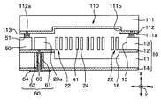
- FIG. 2 is a cross-sectional view taken along line II-II in FIG.
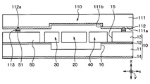
- FIG. 3 is a cross-sectional view taken along line III-III in FIG.
- FIG. 4 is a cross-sectional view taken along line IV-IV in FIG.
- FIG. 5 is a cross-sectional view taken along line VV in FIG. 1.
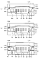
- A)-(e) is sectional drawing which shows the manufacturing process of the acceleration sensor shown in FIG.
- A)-(d) is sectional drawing which shows the manufacturing process of the acceleration sensor shown in FIG.
- FIG. 11 is a cross-sectional view taken along line XII-XII in FIG.
- FIG. 11 is a cross-sectional view taken along line XIII-XIII in FIG.
- wire in FIG. It is a top view of the acceleration sensor in a 3rd embodiment of this indication.
- FIG. 16 is a cross-sectional view taken along line XVI-XVI in FIG. (A)-(f) is sectional drawing which shows the manufacturing process of the acceleration sensor shown in FIG. (A)-(c) is sectional drawing which shows the manufacturing process of the acceleration sensor shown in FIG.
- the acceleration sensor of this embodiment is configured by bonding a cap 110 to a semiconductor substrate 10.
- FIG. 1 is a plan view of the semiconductor substrate 10 in the acceleration sensor.
- the semiconductor substrate 10 is an SOI substrate in which a support substrate 11, a buried insulating film 12, and a semiconductor layer 13 are sequentially stacked, and an insulating film 14 is formed on the surface of the support substrate 11 opposite to the buried insulating film 12 side. It is comprised using.
- the support substrate 11 and the semiconductor layer 13 are made of a silicon substrate, polysilicon or the like, the buried insulating film 12 is made of SiO 2 or SiN, and the insulating film 14 is made of TEOS or the like.
- a well-known micromachine process is performed on the semiconductor layer 13 to form a groove portion 15, and the groove portion 15 forms a comb-shaped beam having a movable portion 20 and first and second fixed portions 30 and 40.
- the structure is partitioned. Further, the support substrate 11 and the buried insulating film 12 are formed with a recessed portion 16 from which portions corresponding to predetermined regions of the movable portion 20 and the first and second fixed portions 30 and 40 are removed.
- the direction along the x-axis is the left-right direction in FIG. 1
- the direction along the y-axis is the direction perpendicular to the direction along the x-axis in the plane of the semiconductor substrate 10.
- the direction along the z-axis is a normal direction to the surface direction of the semiconductor substrate 10.
- the direction along the x-axis is referred to as the x-axis direction
- the direction along the y-axis is referred to as the y-axis direction
- the direction along the z-axis is referred to as the z-axis direction.
- the movable portion 20 has a configuration in which both ends in the longitudinal direction of a rectangular bar-shaped weight portion 21 formed so as to cross over the hollow portion 16 are integrally connected to the anchor portions 23a and 23b via beam portions 22, respectively. ing.
- the anchor portions 23 a and 23 b are fixed to the buried insulating film 12 and supported by the support substrate 11, so that the weight portion 21 and the beam portion 22 in the movable portion 20 face the recessed portion 16. .
- the weight portion 21 is formed so that the longitudinal direction is parallel to the y-axis direction.
- the anchor portion 23 a corresponds to a portion of the semiconductor layer 13 that is electrically connected to the movable electrode 24.
- the beam portion 22 has a rectangular frame shape in which two parallel beams are connected at both ends thereof, and has a spring function of being displaced in a direction perpendicular to the longitudinal direction of the two beams. Specifically, when receiving an acceleration including a component in the y-axis direction, the beam portion 22 displaces the weight portion 21 in the y-axis direction and restores the original state in accordance with the disappearance of the acceleration. ing. Therefore, the weight portion 21 connected to the support substrate 11 via the beam portion 22 can be displaced in the displacement direction of the beam portion 22 on the recess portion 16 in accordance with the application of acceleration.
- the movable portion 20 includes a plurality of movable electrodes 24 that are integrally projected in opposite directions from both side surfaces of the weight portion 21 in a direction orthogonal to the longitudinal direction of the weight portion 21 (x-axis direction). ing.
- four movable electrodes 24 are formed on the left side and the right side of the weight part 21 so as to face the hollow part 16.
- Each movable electrode 24 is formed integrally with the weight portion 21 and the beam portion 22, and can be displaced in the y-axis direction together with the weight portion 21 when the beam portion 22 is displaced.
- the first and second fixed portions 30 and 40 each include a plurality of first and second fixed electrodes 31 and 41 arranged to face each other in parallel with the side surface of the movable electrode 24 so as to have a predetermined detection interval.
- the first and second wiring portions 32 and 42 are configured to be supported so as to sandwich the weight portion 21.
- the four first and second fixed electrodes 31 and 41 are arranged in a comb-like shape so as to mesh with the gaps of the comb teeth in the movable electrode 24 so as to face the recess 16.
- the first and second wiring portions 32 and 42 are supported in a cantilever manner.
- the first and second wiring portions 32 and 42 correspond to portions of the semiconductor layer 13 that are electrically connected to the first and second fixed electrodes 31 and 41.
- the capacitor C s1 is configured between the movable electrode 24 and the first fixed electrode 31, and the capacitor C s2 is configured between the movable electrode 24 and the second fixed electrode 41. Yes. Then, acceleration is detected based on the difference between the capacitors C s1 and C s2 .
- the outer peripheral portion defined by the movable portion 20 and the first and second fixed portions 30 and 40 and the groove portion 15 in the semiconductor layer 13 in the semiconductor substrate 10 is defined as a peripheral portion 50, and the embedded insulating film 12 is interposed therebetween. And supported by the support substrate 11.
- a frame-shaped sealing portion 51 surrounding the movable portion 20 and the first and second fixed portions 30 and 40 is formed.
- This sealing part 51 is comprised with the metal material as an electroconductive member, and is comprised with aluminum etc. in this embodiment.
- the semiconductor substrate 10 is formed with a movable electrode electrode portion 60, first and second fixed electrode electrode portions 70 and 80, and a peripheral electrode portion 90.
- FIG. 4 is a cross section along the first fixing portion 30, but the cross section along the second fixing portion 40 is also the same as that in FIG. 4, and therefore the first and second fixing portions 30 in FIG. 4. , 40 is attached.
- the movable electrode electrode portion 60 passes through the insulating film 62 through the insulating film 14, the support substrate 11, the embedded insulating film 12 and reaches the anchor portion 23 a via the insulating film 62.
- the through electrode 63 is formed, and the pad portion 64 electrically connected to the through electrode 63 is formed on the insulating film 14.
- the first and second fixed electrode electrode portions 70 and 80 penetrate through the insulating film 14, the support substrate 11, and the buried insulating film 12, and the first and second wiring portions.
- Through electrodes 73 and 83 are formed in the first and second fixed electrode hole portions 71 and 81 reaching 32 and 42 through insulating films 72 and 82, and the through electrodes 73 and 83 are electrically connected to the insulating film 14.
- the pad portions 74 and 84 to be connected are formed.
- the peripheral electrode portion 90 passes through the insulating film 14, the support substrate 11, and the buried insulating film 12, and the insulating film 92 is formed in the peripheral hole portion 91 that reaches the peripheral portion 50.
- a through electrode 93 is formed through the pad, and a pad portion 94 that is electrically connected to the through electrode 93 is formed on the insulating film 14.
- the pad portions 64 to 94 formed on the buried insulating film 12 are connected to an external circuit, whereby the movable electrode 24, the first and second fixed electrodes 31, 41, and the peripheral portion 50 are connected. A predetermined potential is applied to the.
- a contact hole 14 a that exposes a predetermined portion of the support substrate 11 is formed in the insulating film 14.
- a contact portion 100 that is electrically connected to the support substrate 11 is formed in the contact hole 14a.
- the contact portion 100 is integrated with the pad portion 94 in the peripheral electrode portion 90 so that the same potential as that of the peripheral portion 50 is applied.
- the insulating films 62 to 92 are made of TEOS or the like, and the through electrodes 63 to 93 and the contact part 100 are made of aluminum or the like.
- the cap 110 is configured using a bonded substrate 111 and an insulating film 112, as shown in FIGS.
- the bonded substrate 111 has a recess 111b formed in a portion facing the movable electrode 24 and the first and second fixed electrodes 31 and 41 in one surface 111a facing the semiconductor substrate 10.
- the insulating film 112 is formed on the one surface 111a of the bonded substrate 111 and the wall surface of the recess 111b.
- a silicon substrate or the like is used as the bonded substrate 111, and SiO 2 or SiN or the like is used as the insulating film 112.
- a sealing portion 113 having a shape corresponding to the sealing portion 51 is formed in a portion facing the sealing portion 51 formed in the peripheral portion 50. That is, the sealing part 113 has a frame shape corresponding to the sealing part 51.
- the sealing portion 113 is electrically connected to the bonded substrate 111 through a contact hole 112 a formed in the insulating film 112.
- this sealing part 113 is comprised with the metal material as an electroconductive member, and is comprised with aluminum etc. in this embodiment.
- the above is the configuration of the cap 110 in the present embodiment.
- the semiconductor substrate 10 and the cap 110 are bonded and integrated to form an acceleration sensor.
- the cap 110 is metal-bonded to the sealing portion 51 in which the sealing portion 113 is formed on the semiconductor substrate 10 so that the movable portion 20 and the first and second fixing portions 30 and 40 are sealed. And integrated with the semiconductor substrate 10.
- the cap 110 (bonded substrate 111) is electrically connected to the peripheral portion 50 by being bonded to the semiconductor substrate 10 via the sealing portions 51 and 113.
- the acceleration sensor of the present embodiment is configured.
- Such an acceleration sensor is mounted on the mounted member such that the side of the cap 110 opposite to the insulating film 112 is in contact with the mounted member, and each pad portion 64 to 94 is connected to an external circuit via a bonding wire or the like. Electrically connected.
- a predetermined potential is applied to the movable electrode 24 and the first and second fixed electrodes 31 and 41 via the pad portions 64 to 84.
- a predetermined potential is applied to the peripheral portion 50, the support substrate 11, and the bonded substrate 111 via the pad portion 94.
- FIGS. 6 to 9 are cross-sectional views corresponding to the line III-III in FIG.
- a support substrate 11 is prepared, and a buried insulating film 12 is formed on the support substrate 11 by a CVD (Chemical Vapor Deposition) method, thermal oxidation, or the like.
- CVD Chemical Vapor Deposition
- a mask such as a resist or an oxide film is formed on the buried insulating film 12 and wet etching or the like is performed, so that the support substrate 11 and the buried substrate are buried.
- the recess 16 is formed in the insulating film 12.
- the buried insulating film 12 and the semiconductor layer 13 are joined by direct joining. That is, first, the bonding surface of the buried insulating film 12 and the bonding surface of the semiconductor layer 13 are irradiated with N 2 plasma, O 2 plasma, or Ar ion beam, and each bonding surface of the buried insulating film 12 and the semiconductor layer 13 is irradiated. Activate. Then, alignment using an infrared microscope or the like is performed using an appropriately formed alignment mark, and the buried insulating film 12 and the semiconductor layer 13 are bonded by direct bonding at room temperature to 1100 ° C.
- the buried insulating film 12 and the semiconductor layer 13 may be bonded by a bonding technique such as anodic bonding, intermediate layer bonding, or fusion bonding. And after joining, you may perform the process which improves joining quality, such as high temperature annealing. Furthermore, after bonding, the support substrate 11 and the semiconductor layer 13 may be processed to a desired thickness by grinding and polishing.
- a metal film is formed on the semiconductor layer 13 by a CVD method or the like. Then, reactive ion etching using a mask (not shown) such as a resist or an oxide film is performed, and the sealing portion 51 is formed by patterning the metal film.
- the sealing portion 51 is formed in the semiconductor layer 13, and when the movable portion 20 and the first and second fixed portions 30 and 40 are formed, heat between the semiconductor layer 13 and the sealing portion 51 is formed. Thermal stress may be applied to the semiconductor layer 13 due to the difference in expansion coefficient. However, since the sealing portion 51 is formed on the semiconductor layer 13 and can expand and contract as compared with the conventional case where the through electrode is embedded in the semiconductor layer, the semiconductor portion 13 The thermal stress applied to the layer 13 is small. For this reason, in this process, the processing accuracy of the movable portion 20 and the first and second fixed portions 30 and 40 is unlikely to decrease.
- a bonded substrate 111 is prepared as shown in FIG. 7A, and one surface 111a of the bonded substrate 111 is shown in FIG. 7B.
- a recess 111b is formed in the bottom.
- the recess 111b can be formed by wet etching using a mask (not shown) such as a resist or an oxide film.
- an insulating film 112 is formed on the one surface 111a of the bonded substrate 111 by thermal oxidation or the like.
- a sealing portion 113 that is electrically connected to the bonded substrate 111 through the contact hole 112a is formed.
- a sealing portion 113 that is electrically connected to the bonded substrate 111 through the contact hole 112a is formed.
- a mask such as a resist or an oxide film (not shown) to form a contact hole 112 a in the insulating film 112.
- a metal film is formed over the insulating film 112 so that the metal film is embedded in the contact hole 112a.
- reactive ion etching or the like using a mask (not shown) such as a resist or an oxide film is performed, and the sealing portion 113 is formed by patterning the metal film.
- the semiconductor substrate 10 and the cap 110 are joined. Specifically, alignment is performed by an infrared microscope or the like using an appropriately formed alignment mark, and the sealing portion 51 of the semiconductor substrate 10 and the sealing portion 113 of the cap 110 are metal-bonded at 300 to 500 ° C.
- first hole portions 17a reaching the buried insulating film 12 from the opposite side of the supporting substrate 11 to the buried insulating film 12 side are formed.
- a first hole portion 17a that reaches the buried insulating film 12 is formed in the support substrate 11 at a portion of the support substrate 11 that faces the anchor portion 23a.
- the support substrate 11 has two portions reaching the buried insulating film 12 in the portions of the support substrate 11 facing the first and second wiring portions 32 and 42.
- a first hole 17a is formed.
- a first hole portion 17 a that reaches the buried insulating film 12 is formed in the support substrate 11 at a portion of the support substrate 11 that faces the peripheral portion 50.
- an insulating film 62 is formed on the wall surface of the first hole portion 17a by the CVD method or the like.
- insulating films 72 to 92 are formed on the wall surface of each first hole portion 17a in a cross section different from FIG.
- the insulating film 14 is composed of an insulating film formed on the support substrate 11 on the side opposite to the buried insulating film 12. That is, the insulating film 14 and the insulating films 62 to 92 are formed in the same process.
- the semiconductor substrate 10 in which the insulating film 14, the support substrate 11, the buried insulating film 12, and the semiconductor layer 13 are sequentially stacked is configured.
- a second hole portion 17b that exposes the anchor portion 23a is formed in the buried insulating film 12 located at the bottom of the first hole portion 17a.
- the movable electrode hole 61 is configured by the first and second holes 17a and 17b.
- the second wiring portion 32, 42 or the peripheral portion 50 is exposed to the buried insulating film 12 located at the bottom of each first hole portion 17a.
- the hole 17b is formed.
- the first and second fixed electrode holes 71 and 81 and the peripheral hole 91 are formed in the first and second holes 17a and 17b.
- a contact hole 14a is formed in the insulating film 14 in a cross section different from that of FIG.
- Each second hole 17b and contact hole 14a are formed simultaneously.
- a through electrode 63 is formed by forming a metal film in the movable electrode hole 61 by sputtering or vapor deposition. Further, in a cross section different from FIG. 9B, metal films are formed in the first and second fixed electrode holes 71 and 81 and the peripheral hole 91 to form the through electrodes 73 to 93. At the same time, a metal film is formed in the contact hole 14 a to form the contact portion 100. Thereafter, the metal film on the insulating film 14 is patterned to form the pad portion 64. Further, pad portions 74 to 94 are formed in a cross section different from that in FIG. As described above, the acceleration sensor of this embodiment is manufactured.
- the through electrodes 63 to 93 and the contact part 100 are formed in the same process of forming a metal film, and the pad parts 64 to 94 are formed in the same process of patterning the metal film. Moreover, although the manufacturing method of one acceleration sensor was demonstrated above, after performing the said process in a wafer state, you may make it dice cut and divide
- the contact portion 100 is formed on the support substrate 11, and the support substrate 11 is maintained at a predetermined potential via the contact portion 100. That is, it is not necessary to form a through electrode for maintaining the support substrate 11 at a predetermined potential inside the semiconductor layer 13. For this reason, when forming the movable part 20 and the 1st, 2nd fixing
- the movable electrode electrode part 60, the first and second fixed electrode electrode parts 70 and 80, and the peripheral electrode part 90 are formed on the semiconductor substrate 10.
- the contact portion 100 is formed simultaneously with the movable electrode portion 60, the first and second fixed electrode portions 70 and 80, and the peripheral portion electrode portion 90. For this reason, it is not necessary to add a manufacturing process only for forming the contact part 100, and a manufacturing process does not increase.
- the contact part 100 is integrated with the pad part 94 in the peripheral electrode part 90. For this reason, it is not necessary to form a new pad portion in order to connect the contact portion 100 and the external circuit.
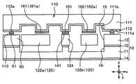
- the movable portion 120 is defined by the groove portion 15 in the semiconductor layer 13.
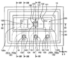
- FIG. 10 is a plan view of the semiconductor substrate 10 in the acceleration sensor.
- the movable electrode wiring portion 151, the first wiring portion 161, and the second wiring portion 161, which will be described later, provided in the cap 110 are indicated by dotted lines. is there.
- the movable part 120 has a rectangular frame-shaped frame part 122 in which a planar rectangular opening part 121 is formed, and a torsion beam 123 provided so as to connect opposite sides of the opening part 121.
- the movable portion 120 is supported by the support substrate 11 by connecting the torsion beam 123 to the anchor portion 124 supported by the buried insulating film 12.
- the direction along the x-axis is the left-right direction in FIG. 10
- the direction along the y-axis is the direction perpendicular to the direction along the x-axis in the plane of the semiconductor substrate 10, and is along the z-axis.
- the direction is a normal direction to the surface direction of the semiconductor substrate 10.
- the direction along the x-axis is referred to as the x-axis direction
- the direction along the y-axis is referred to as the y-axis direction
- the direction along the z-axis is referred to as the z-axis direction.
- the torsion beam 123 is a member that becomes a rotation axis that becomes the rotation center of the movable part 120 when an acceleration in the z-axis direction is applied, and is provided so as to divide the opening 121 into two in this embodiment.
- the frame portion 122 has an asymmetric shape with respect to the torsion beam 123 so that it can rotate around the torsion beam 123 when an acceleration in the z-axis direction is applied.
- the length of the frame portion 122 in the x-axis direction to the end of the portion farthest from the torsion beam 123 in the first portion 122a is farthest from the torsion beam 123 in the second portion 122b. It is longer than the length in the x-axis direction to the end of the part. That is, in the frame portion 122 of the present embodiment, the mass of the first part 122a is larger than the mass of the second part 122b.
- the movable electrode 125 is configured in a portion of the frame portion 122 that faces first and second fixed electrodes 161a and 162a described later.
- the support substrate 11 and the buried insulating film 12 have a recess 16 formed in a portion facing the movable portion 120.
- the movable electrode connection portion 131 and the first and second fixed electrode connection portions 132 and 133 are defined by the groove portion 18.
- the movable electrode connecting portion 131 corresponds to a portion of the semiconductor layer 13 of the present disclosure that is electrically connected to the movable electrode 125.
- the first and second fixed electrode connection portions 132 and 133 correspond to portions of the semiconductor layer 13 of the present disclosure that are electrically connected to the first and second fixed electrodes 161a and 162a.
- the semiconductor layer 13 includes the sealing portion 51 formed in the peripheral portion 50, the anchor portion 124, the movable electrode connection portion 131, the first and second fixed electrode connection portions 132, 133, and the pad portions 141 to 144 is formed.
- Each pad portion 141 to 144 is made of aluminum or the like.
- a movable electrode electrode portion 60 that is electrically connected to the movable electrode connection portion 131 is formed on the semiconductor substrate 10.
- the semiconductor substrate 10 includes first and second fixed electrode electrode portions 70 and 80 that are electrically connected to the first and second fixed electrode connection portions 132 and 133. Is formed.
- the semiconductor substrate 10 is formed with a peripheral electrode portion 90 that is electrically connected to the peripheral portion 50, and a contact that is electrically connected to the support substrate 11. Part 100 is formed.
- FIG. 13 is a cross section taken along a first wiring part 161 to be described later, but the cross section taken along a second wiring part 162 described later is also the same as that shown in FIG. Reference numerals of the two fixed electrode connecting portions 132 and 133 and the first and second wiring portions 161 and 162 are given.
- the cap 110 has a bonded substrate 111 and an insulating film 112 as in the first embodiment. Then, on the insulating film 112, as shown in FIG. 12, the portion facing the pad portion 141 formed on the anchor portion 124 faces the pad portion 142 formed on the movable electrode connection portion 131. A movable electrode wiring portion 151 is formed over the portion.
- first and second wiring portions 161 and 162 made of aluminum or the like are formed.
- the first wiring portion 161 includes a first fixed electrode 161a formed in a portion facing the first portion 122a, and a first lead wiring 161b drawn from the first fixed electrode 161a.
- the second wiring portion 162 includes a second fixed electrode 162a formed in a portion facing the second portion 122b, and a second lead wiring 162b drawn from the second fixed electrode 162a.
- the capacitor C s1 is configured between the first part 122a (movable electrode 125) and the first fixed electrode 161a, and the second part 122b (movable electrode 125), the second fixed electrode 162a, A capacitor C s2 is formed between the two. Then, acceleration is detected based on the difference between the capacitors C s1 and C s2 .
- the first and second fixed electrodes 161a and 162a have the same planar shape, and are formed so as to form an equal capacity with the movable electrode 125 when no acceleration is applied.
- the first and second lead wires 161b and 162b are extended to a portion of the insulating film 112 that faces the first and second fixed electrode connection portions 132 and 133.
- a recess 111b is appropriately formed in a part of the one surface 111a that faces the frame part 122 and is different from the part where the first and second fixed electrodes 161a and 162a are formed. Has been.
- the semiconductor substrate 10 and the cap 110 are joined and integrated to form the acceleration sensor of this embodiment.
- the sealing portions 51 and 113 are metal-bonded, the pad portions 141 and 142, the movable electrode wiring portion 151, the pad portions 143 and 144, and the first,
- the second lead wires 161b and 161b are integrated by metal bonding.
- the movable electrode 125 (via the movable electrode connection portion 131, the pad portion 142, the movable electrode wiring portion 151, and the pad portion 142).
- a predetermined potential is applied to the anchor portion 124).
- the first and second fixed electrode connection portions 132 and 133 and the pad portions 143 and 144 are provided.
- a predetermined potential is applied to the first and second fixed electrodes 161a and 162a through the first and second lead wires 161b and 162b.
- a predetermined potential is applied to the pad portion 94 of the peripheral electrode portion 90
- a predetermined potential is applied to the peripheral portion 50 and the support substrate 11, and the bonded substrate 111 is interposed via the sealing portions 51 and 113.
- the potential of the peripheral portion 50 is applied to
- Such an acceleration sensor forms the pad portions 141 to 144 together with the sealing portion 51 in the step (d) of FIG. 6E, the groove portion 15 is formed in the semiconductor layer 13 to form the movable portion 120, and the groove portion 18 is formed in the semiconductor layer 13 to form the movable electrode connection portion 131, the first, Second fixed electrode connection portions 132 and 133 are formed.
- the sealing portion 113 is formed, and the movable electrode wiring portion 151 and the first and second wiring portions 161 and 162 are formed.
- the movable electrode electrode part 60 connected to the movable electrode connection part 131, the first and second fixed electrode connection parts 132 and 133 connected to the first and second fixed electrode connection parts 132 and 133. What is necessary is just to form the electrode parts 70 and 80 for fixed electrodes.
- the present disclosure can also be applied to an acceleration sensor that detects acceleration in the normal direction (z-axis direction) with respect to the surface direction of the semiconductor substrate 10.
- the bonded substrate 111 has a portion that is opposed to the frame portion 122 of the one surface 111a and that is different from the portion where the first and second fixed electrodes 161a and 162a are formed.
- a recess 111b is formed. That is, the gap between the cap 110 and a portion different from the portion that becomes the movable electrode 125 in the frame portion 122 is widened. For this reason, the parasitic capacitance generated between the frame portion 122 and the cap 110 can be reduced, and the detection accuracy can be improved.
- a third embodiment of the present disclosure will be described.
- the present embodiment is different from the first embodiment in that a recess is formed from the opposite side of the support substrate 11 to the buried insulating film 12 side, and the rest is the same as the first embodiment. Therefore, the description is omitted here.
- the support substrate 11, the buried insulating film 12, and the semiconductor layer 13 are laminated in this order to constitute the semiconductor substrate 10.
- the semiconductor substrate 10 is provided with a recess 19 that exposes the semiconductor layer 13 from the side of the support substrate 11 opposite to the buried insulating film 12 side.
- the hollow portion 19 is formed so as to expose the anchor portion 23a, a portion of the first and second wiring portions 32 and 42, and a portion of the peripheral portion 50 in a lump.
- this hollow part 19 is formed away from the hollow part 16.
- Pad portions 171 to 174 are formed in portions of the anchor portion 23a, the first and second wiring portions 32 and 42, and the peripheral portion 50 that are exposed from the recess portion 19. Further, the pad portion 174 formed in the peripheral portion 50 is extended to the opposite side of the support substrate 11 exposed from the recess portion 19 and the buried insulating film 12 side of the support substrate 11. A contact portion 100 is formed at a portion that contacts the support substrate 11. That is, the same potential as that of the peripheral portion 50 is applied to the support substrate 11.
- FIGS. 17 and 18 are cross-sectional views corresponding to the XVI-XVI line in FIG.
- the buried insulating film 12 is formed on the support substrate 11, and as shown in FIG. One depression 19a is formed.
- the first dent 19 a is formed in the same process as the dent 16.
- the semiconductor layer 13 is prepared, and a metal film is formed on the semiconductor layer 13 on the side to be joined to the buried insulating film 12. Then, reactive ion etching or the like using a mask (not shown) such as a resist or an oxide film is performed, and the metal film is patterned to thereby fix the anchor portion 23a, the first and second wiring portions 32 and 42, and the peripheral portion.
- the pad portions 171 to 174 are formed in the 50 formation scheduled regions.
- the buried insulating film 12 and the semiconductor layer 13 are joined by performing the same process as in FIG. 6C. At this time, the buried insulating film 12 and the semiconductor layer 13 are bonded so that the pad portions 171 to 174 are accommodated in the first recess portion 19a.
- FIG. 17E and FIG. 17F the same steps as in FIG. 6D and FIG. 6E are performed to form the sealing portion 51.
- the movable portion 20 and the first and second fixed portions 30 and 40 are formed.
- step of FIG. 7 is performed and the cap 110 is prepared, as shown in FIG. 18A
- step similar to that of FIG. 8A is performed to perform the semiconductor layer 13 and the cap 110. And join.
- a through hole 19c reaching the pad portion 174 from the opposite side of the support substrate 11 to the buried insulating film 12 side is formed.
- a metal film is formed in the through hole 19c by a mask vapor deposition method or the like.
- the pad portion 174 is integrated with a portion of the through-hole 19c that constitutes the wall surface of the support substrate 11 exposed from the recess portion 19 when the step (c) of FIG.
- a contact portion 100 is formed by forming a metal film as described above. Then, the metal film formed on the support substrate 11 on the side opposite to the buried insulating film 12 is patterned.
- a second recess portion 19 b communicating with the first recess portion 19 a is formed from the opposite side of the support substrate 11 to the buried insulating film 12 side to form the recess portion 19.
- the anchor part 23a, the first and second wiring parts 32, 42, the recessed portion 19 that exposes the peripheral portion 50 may be formed, and the pad portions 171 to 174 and the contact portion 100 may be formed in the portion exposed from the recessed portion 19. Even with such an acceleration sensor, the same effect as in the first embodiment can be obtained.
- the acceleration sensor as the physical quantity sensor has been described, but the present disclosure can be applied to an angular velocity sensor as the physical quantity sensor.
- the cap 110 may not have the insulating film 112. That is, the sealing portion 113 may be formed on the one surface 111 a of the bonded substrate substrate 111.
- the insulating layer 112 is not formed on the bonded substrate 111, and the peripheral portion 50 of the semiconductor layer 13 and the bonded substrate 111 are bonded by direct bonding or the like. And the bonded substrate 111 may be electrically connected.
- the contact part 100 and the pad part 94 in the peripheral electrode part 90 may not be integrated.
- the contact portion 100 extends to the side opposite to the buried insulating film 12 side of the support substrate 11 has been described.
- the contact portion 100 is exposed from the hollow portion 19. It may be formed only on the substrate 11. Further, the contact part 100 may be formed only on a part of the support substrate 11 opposite to the buried insulating film 12 side.
- the peripheral portion 50 and the cap 110 may not be electrically connected.
- the bonded substrate 111 may be maintained at a predetermined potential by forming a contact portion electrically connected to an external circuit on the bonded substrate 111.
- a plurality of through electrodes are formed in the cap 110, and the movable electrodes 24 and 125, the fixed electrodes 31, 41, 161 a and 162 a, and the peripheral portion 50 are formed through the through electrodes formed in the cap 110.
- a predetermined potential may be applied.
- the third embodiment is combined with the second embodiment, and instead of forming the movable electrode portion 60, the first and second fixed electrode portions 70 and 80, and the peripheral portion electrode portion 90, the depression portion is formed. 19 may be formed.
Landscapes
- Physics & Mathematics (AREA)
- General Physics & Mathematics (AREA)
- Engineering & Computer Science (AREA)
- Microelectronics & Electronic Packaging (AREA)
- Electromagnetism (AREA)
- Computer Hardware Design (AREA)
- Pressure Sensors (AREA)
- Manufacturing & Machinery (AREA)
Abstract
Description
本開示の第1実施形態について図面を参照しつつ説明する。なお、本実施形態では、エアバッグ、ABS(Antilock Brake System)、ESC(Electronic Stability Control)等の作動制御を行うための加速度センサに本開示の物理量センサを適用した例を説明する。
本開示の第2実施形態について説明する。本実施形態は、第1実施形態に対して、半導体基板10の面方向に対する法線方向の加速度を検出する加速度センサに本開示を適用したものであり、その他に関しては第1実施形態と同様であるため、ここでは説明を省略する。
本開示の第3実施形態について説明する。本実施形態は、第1実施形態に対して、支持基板11のうちの埋込絶縁膜12側と反対側から窪み部が形成されているものであり、その他に関しては第1実施形態と同様であるため、ここでは説明を省略する。
本開示は、実施例に準拠して記述されたが、本開示は当該実施例や構造に限定されるものではないと理解される。本開示は、様々な変形例や均等範囲内の変形をも包含する。加えて、様々な組み合わせや形態、さらには、それらに一要素のみ、それ以上、あるいはそれ以下、を含む他の組み合わせや形態をも、本開示の範疇や思想範囲に入るものである。
Claims (11)
- 支持基板(11)と、前記支持基板上に配置された埋込絶縁膜(12)と、前記埋込絶縁膜を挟んで前記支持基板と反対側に配置された半導体層(13)と、を有する半導体基板(10)と、
前記半導体層に設けられ、物理量に応じて変位する可動電極(24、125)と、
前記半導体層のうち前記可動電極を囲むと共に前記可動電極と区画された周辺部(50)と、
前記可動電極と対向して配置された固定電極(31、41、161a、162a)と、
前記半導体層と接合されて前記可動電極を封止するキャップ(110)と、を備え、
前記支持基板および前記キャップが所定電位に維持されており、
前記支持基板は、外部回路と直接電気的に接続されるコンタクト部(100)を有し、前記コンタクト部を介して所定電位に維持されている物理量センサ。 - 前記支持基板および前記埋込絶縁膜には、前記支持基板のうちの前記埋込絶縁膜側と反対側から前記半導体層のうちの前記可動電極と電気的に接続される部分(23a、131)に達する可動電極用孔部(61)、前記固定電極と電気的に接続される部分(32、42、132、133)に達する固定電極用孔部(71、81)、前記周辺部に達する周辺部用孔部(91)が設けられ、
前記可動電極用孔部、前記固定電極用孔部、前記周辺部用孔部には、それぞれ絶縁膜(62~92)を介して外部回路と電気的に接続される貫通電極(63~93)が配置され、
前記キャップは、前記周辺部と電気的に接続されることで所定電位に維持されている請求項1に記載の物理量センサ。 - 前記周辺部用孔部に配置された貫通電極は、パッド部(94)を介して前記外部回路と電気的に接続されており、
前記コンタクト部は、前記パッド部と一体化されている請求項2に記載の物理量センサ。 - 前記支持基板および前記埋込絶縁膜には、前記支持基板のうちの前記埋込絶縁膜側と反対側から前記半導体層のうちの前記可動電極と電気的に接続される部分(23a、131)、前記固定電極と電気的に接続される部分(32、42、132、133)、前記周辺部を一括的に露出させる窪み部(19)が設けられ、
前記半導体層のうちの前記窪み部から露出する前記可動電極と電気的に接続される部分、前記固定電極と電気的に接続される部分、前記周辺部には、外部回路と電気的に接続されるパッド部(171~174)が設けられており、
前記キャップは、前記周辺部と電気的に接続されることで所定電位に維持されている請求項1に記載の物理量センサ。 - 前記窪み部から露出する前記周辺部に設けられた前記パッド部は、前記窪み部から露出する前記支持基板まで延設されて前記コンタクト部を形成している請求項4に記載の物理量センサ。
- 前記周辺部には前記可動電極を囲む導電性部材で構成された封止部(51)が設けられていると共に、前記キャップには前記封止部と対応する形状であって導電性部材で構成された封止部(113)が設けられ、
前記周辺部および前記キャップは、それぞれの前記封止部が接合されることによって電気的に接続されている請求項1ないし5のいずれか1つに記載の物理量センサ。 - 前記可動電極(24)は、前記半導体基板の面方向と平行な方向の物理量に応じて変位し、
前記固定電極(31、41)は、前記半導体層に設けられていると共に前記周辺部と区画されている請求項1ないし6のいずれか1つに記載の物理量センサ。 - 前記可動電極(125)は、前記半導体基板の面方向に対する法線方向の物理量に応じて変位し、
前記固定電極(161a、162a)は、前記キャップのうちの前記可動電極と対向する部分に設けられている請求項1ないし6のいずれか1つに記載の物理量センサ。 - 前記可動電極は、前記半導体層に設けられた枠部(122)の一部で構成され、
前記キャップは、前記枠部と対向する部分であって、前記固定電極が設けられる部分と異なる部分に窪み部(111b)が設けられている請求項8に記載の物理量センサ。 - 支持基板(11)と、前記支持基板上に配置された埋込絶縁膜(12)と、前記埋込絶縁膜を挟んで前記支持基板と反対側に配置された半導体層(13)と、を有する半導体基板(10)と、
前記半導体層に設けられ、物理量に応じて変位する可動電極(24、125)と、
前記半導体層のうち前記可動電極を囲むと共に前記可動電極と区画された周辺部(50)と、
前記可動電極と対向して配置された固定電極(31、41、161a、162a)と、
前記半導体層と接合されて前記可動電極を封止するキャップ(110)と、を備え、
前記支持基板および前記キャップが所定電位に維持されており、
前記支持基板には、外部回路と直接電気的に接続されるコンタクト部(100)が設けられ、
前記支持基板および前記埋込絶縁膜には、前記支持基板のうちの前記埋込絶縁膜側と反対側から前記半導体層のうちの前記可動電極と電気的に接続される部分(23a、131)に達する可動電極用孔部(61)、前記固定電極と電気的に接続される部分(32、42、132、133)に達する固定電極用孔部(71、81)、前記周辺部に達する周辺部用孔部(91)が設けられ、
前記可動電極用孔部、前記固定電極用孔部、前記周辺部用孔部には、それぞれ絶縁膜(62~92)を介して外部回路と電気的に接続される貫通電極(63~93)が配置されている物理量センサの製造方法において、
前記半導体基板を用意することと、
前記半導体層に前記可動電極および前記周辺部を区画形成することと、
前記半導体層のうちの前記周辺部と前記キャップとが電気的に接続されるように、前記半導体層と前記キャップとを接合することと、
前記支持基板に、前記埋込絶縁膜側と反対側から前記支持基板のうちの前記可動電極と電気的に接続される部分と対向する部分、前記固定電極と電気的に接続される部分と対向する部分、前記周辺部と対向する部分に前記埋込絶縁膜に達する第1孔部(17a)を形成することと、
前記第1孔部に前記絶縁膜を形成すると共に前記支持基板のうちの前記埋込絶縁膜側と反対側の部分に絶縁膜(14)を形成することと、
前記第1孔部の底部に位置する前記埋込絶縁膜に第2孔部(17b)を形成することにより、前記第1、第2孔部にて前記可動電極用孔部、前記固定電極用孔部、前記周辺部用孔部を形成すると共に、前記支持基板のうちの前記埋込絶縁膜と反対側の部分に形成された前記絶縁膜に前記支持基板を露出させるコンタクトホール(14a)を形成することと、
前記可動電極用孔部、前記固定電極用孔部、前記周辺部用孔部に前記絶縁膜を介して前記貫通電極を形成すると共に、前記コンタクトホールに前記コンタクト部を形成することと、を有する物理量センサの製造方法。 - 支持基板(11)と、前記支持基板上に配置された埋込絶縁膜(12)と、前記埋込絶縁膜を挟んで前記支持基板と反対側に配置された半導体層(13)と、を有する半導体基板(10)と、
前記半導体層に設けられ、物理量に応じて変位する可動電極(24、125)と、
前記半導体層のうち前記可動電極を囲むと共に前記可動電極と区画された周辺部(50)と、
前記可動電極と対向して配置された固定電極(31、41、161a、162a)と、
前記半導体層と接合されて前記可動電極を封止するキャップ(110)と、を備え、
前記支持基板および前記キャップが所定電位に維持されており、
前記支持基板には、外部回路と直接電気的に接続されるコンタクト部(100)が設けられ、
前記支持基板および前記埋込絶縁膜には、前記支持基板のうちの前記埋込絶縁膜と反対側から前記半導体層のうちの前記可動電極と電気的に接続される部分(23a、131)、前記固定電極と電気的に接続される部分(32、42、132、133)、前記周辺部を一括的に露出させる窪み部(19)が設けられ、
前記窪み部から露出する前記可動電極と電気的に接続される部分、前記固定電極と電気的に接続される部分、前記周辺部には、外部回路と電気的に接続されるパッド部(171~174)が設けられている物理量センサの製造方法において、
前記支持基板上に前記埋込絶縁膜を形成し、前記埋込絶縁膜側から前記窪み部の一部を構成する第1窪み部(19a)を形成することと、
前記半導体層のうちの前記可動電極と電気的に接続される部分、前記固定電極と電気的に接続される部分、前記周辺部の形成予定領域に前記パッド部を形成することと、
前記パッド部が前記第1窪み部内に収容されるように、前記埋込絶縁膜と前記半導体層とを接合することと、
前記半導体層に前記可動電極および前記周辺部を区画形成することと、
前記半導体層のうちの周辺部と前記キャップとが電気的に接続されるように、前記半導体層と前記キャップとを接合することと、
前記支持基板に、前記埋込絶縁膜側と反対側から前記周辺部に形成された前記パッド部を露出させる貫通孔(19c)を形成することと、
前記貫通孔に前記周辺部に形成された前記パッド部と連結される前記コンタクト部を形成することと、
前記支持基板に、前記第1窪み部と連通する第2窪み部(19b)を形成することにより、前記第1、第2窪み部にて前記窪み部を形成することと、を有する物理量センサの製造方法。
Priority Applications (2)
| Application Number | Priority Date | Filing Date | Title |
|---|---|---|---|
| US15/022,954 US10338092B2 (en) | 2013-09-26 | 2014-09-23 | Physical quantity sensor and method for manufacturing the same |
| DE112014004474.1T DE112014004474T5 (de) | 2013-09-26 | 2014-09-23 | Sensor für eine physikalische Grösse und Verfahren zur Herstellung derselben |
Applications Claiming Priority (2)
| Application Number | Priority Date | Filing Date | Title |
|---|---|---|---|
| JP2013200068A JP6123613B2 (ja) | 2013-09-26 | 2013-09-26 | 物理量センサおよびその製造方法 |
| JP2013-200068 | 2013-09-26 |
Publications (1)
| Publication Number | Publication Date |
|---|---|
| WO2015045360A1 true WO2015045360A1 (ja) | 2015-04-02 |
Family
ID=52742532
Family Applications (1)
| Application Number | Title | Priority Date | Filing Date |
|---|---|---|---|
| PCT/JP2014/004859 Ceased WO2015045360A1 (ja) | 2013-09-26 | 2014-09-23 | 物理量センサおよびその製造方法 |
Country Status (4)
| Country | Link |
|---|---|
| US (1) | US10338092B2 (ja) |
| JP (1) | JP6123613B2 (ja) |
| DE (1) | DE112014004474T5 (ja) |
| WO (1) | WO2015045360A1 (ja) |
Cited By (1)
| Publication number | Priority date | Publication date | Assignee | Title |
|---|---|---|---|---|
| WO2018003353A1 (ja) * | 2016-07-01 | 2018-01-04 | 株式会社デンソー | 半導体装置 |
Families Citing this family (4)
| Publication number | Priority date | Publication date | Assignee | Title |
|---|---|---|---|---|
| JP6401728B2 (ja) * | 2016-03-18 | 2018-10-10 | 株式会社日立製作所 | 慣性センサおよびその製造方法 |
| JP6932491B2 (ja) * | 2016-10-31 | 2021-09-08 | 株式会社豊田中央研究所 | Mems装置を製造する方法 |
| JP6540751B2 (ja) * | 2017-06-15 | 2019-07-10 | 株式会社デンソー | 物理量センサ |
| JP7176353B2 (ja) * | 2018-10-29 | 2022-11-22 | セイコーエプソン株式会社 | 物理量センサー、電子機器および移動体 |
Citations (7)
| Publication number | Priority date | Publication date | Assignee | Title |
|---|---|---|---|---|
| JP2010127763A (ja) * | 2008-11-27 | 2010-06-10 | Hitachi Ltd | 半導体力学量検出センサ及びそれを用いた制御装置 |
| JP2010139495A (ja) * | 2008-11-13 | 2010-06-24 | Denso Corp | 半導体装置およびその製造方法 |
| JP2010145212A (ja) * | 2008-12-18 | 2010-07-01 | Denso Corp | 半導体装置 |
| JP2010223640A (ja) * | 2009-03-20 | 2010-10-07 | Denso Corp | 半導体装置およびその製造方法 |
| WO2012020739A1 (ja) * | 2010-08-11 | 2012-02-16 | 日立オートモティブシステムズ株式会社 | 慣性センサ |
| JP2012183612A (ja) * | 2011-03-07 | 2012-09-27 | Toyota Central R&D Labs Inc | Memsデバイス |
| JP2012186300A (ja) * | 2011-03-04 | 2012-09-27 | Denso Corp | 領域分割基板およびそれを用いた半導体装置ならびにそれらの製造方法 |
Family Cites Families (19)
| Publication number | Priority date | Publication date | Assignee | Title |
|---|---|---|---|---|
| EP0459723B1 (en) * | 1990-05-30 | 1996-01-17 | Hitachi, Ltd. | Semiconductor acceleration sensor and vehicle control system using the same |
| DE4419844B4 (de) * | 1994-06-07 | 2009-11-19 | Robert Bosch Gmbh | Beschleunigungssensor |
| JP4003326B2 (ja) * | 1998-02-12 | 2007-11-07 | 株式会社デンソー | 半導体力学量センサおよびその製造方法 |
| DE10066435B4 (de) * | 1999-07-26 | 2012-03-08 | Denso Corporation | Halbleitersensor für eine physikalische Größe |
| US7469588B2 (en) * | 2006-05-16 | 2008-12-30 | Honeywell International Inc. | MEMS vertical comb drive with improved vibration performance |
| JP5092462B2 (ja) * | 2006-06-13 | 2012-12-05 | 株式会社デンソー | 力学量センサ |
| JP2007333641A (ja) * | 2006-06-16 | 2007-12-27 | Sony Corp | 慣性センサおよび慣性センサの製造方法 |
| JP4825778B2 (ja) | 2007-11-16 | 2011-11-30 | 株式会社日立製作所 | 半導体装置およびその製造方法 |
| JP2009216693A (ja) * | 2008-02-13 | 2009-09-24 | Denso Corp | 物理量センサ |
| JP4636187B2 (ja) * | 2008-04-22 | 2011-02-23 | 株式会社デンソー | 力学量センサの製造方法および力学量センサ |
| US8089144B2 (en) * | 2008-12-17 | 2012-01-03 | Denso Corporation | Semiconductor device and method for manufacturing the same |
| JP4784641B2 (ja) * | 2008-12-23 | 2011-10-05 | 株式会社デンソー | 半導体装置およびその製造方法 |
| JP2010223952A (ja) * | 2009-02-24 | 2010-10-07 | Seiko Epson Corp | 加速度センサー、電子機器 |
| JP2010238921A (ja) | 2009-03-31 | 2010-10-21 | Alps Electric Co Ltd | Memsセンサ |
| EP2375219B1 (en) | 2009-04-17 | 2019-02-20 | Hitachi, Ltd. | Inertial sensor and method for manufacturing the same |
| JP5218455B2 (ja) * | 2010-03-17 | 2013-06-26 | 株式会社デンソー | 半導体力学量センサおよびその製造方法 |
| JP5425824B2 (ja) * | 2011-02-16 | 2014-02-26 | 日立オートモティブシステムズ株式会社 | 複合センサ |
| JP5942554B2 (ja) * | 2012-04-11 | 2016-06-29 | セイコーエプソン株式会社 | 物理量センサーおよび電子機器 |
| JP5967018B2 (ja) * | 2013-05-31 | 2016-08-10 | 株式会社デンソー | 容量式物理量センサ |
-
2013
- 2013-09-26 JP JP2013200068A patent/JP6123613B2/ja not_active Expired - Fee Related
-
2014
- 2014-09-23 US US15/022,954 patent/US10338092B2/en not_active Expired - Fee Related
- 2014-09-23 WO PCT/JP2014/004859 patent/WO2015045360A1/ja not_active Ceased
- 2014-09-23 DE DE112014004474.1T patent/DE112014004474T5/de not_active Withdrawn
Patent Citations (7)
| Publication number | Priority date | Publication date | Assignee | Title |
|---|---|---|---|---|
| JP2010139495A (ja) * | 2008-11-13 | 2010-06-24 | Denso Corp | 半導体装置およびその製造方法 |
| JP2010127763A (ja) * | 2008-11-27 | 2010-06-10 | Hitachi Ltd | 半導体力学量検出センサ及びそれを用いた制御装置 |
| JP2010145212A (ja) * | 2008-12-18 | 2010-07-01 | Denso Corp | 半導体装置 |
| JP2010223640A (ja) * | 2009-03-20 | 2010-10-07 | Denso Corp | 半導体装置およびその製造方法 |
| WO2012020739A1 (ja) * | 2010-08-11 | 2012-02-16 | 日立オートモティブシステムズ株式会社 | 慣性センサ |
| JP2012186300A (ja) * | 2011-03-04 | 2012-09-27 | Denso Corp | 領域分割基板およびそれを用いた半導体装置ならびにそれらの製造方法 |
| JP2012183612A (ja) * | 2011-03-07 | 2012-09-27 | Toyota Central R&D Labs Inc | Memsデバイス |
Cited By (1)
| Publication number | Priority date | Publication date | Assignee | Title |
|---|---|---|---|---|
| WO2018003353A1 (ja) * | 2016-07-01 | 2018-01-04 | 株式会社デンソー | 半導体装置 |
Also Published As
| Publication number | Publication date |
|---|---|
| US20160223582A1 (en) | 2016-08-04 |
| DE112014004474T5 (de) | 2016-06-09 |
| US10338092B2 (en) | 2019-07-02 |
| JP6123613B2 (ja) | 2017-05-10 |
| JP2015068646A (ja) | 2015-04-13 |
Similar Documents
| Publication | Publication Date | Title |
|---|---|---|
| US9791472B2 (en) | Acceleration sensor | |
| CN103823082B (zh) | 制造电容式加速度传感器的方法和电容式加速度传感器 | |
| JP6020341B2 (ja) | 容量式物理量センサおよびその製造方法 | |
| JP6123613B2 (ja) | 物理量センサおよびその製造方法 | |
| WO2015019589A1 (ja) | 力学量センサ | |
| WO2017077869A1 (ja) | 力学量センサ | |
| US9446938B2 (en) | SOI substrate, physical quantity sensor, SOI substrate manufacturing method, and physical quantity sensor manufacturing method | |
| JP2009250874A (ja) | 物理量センサおよびその製造方法 | |
| US10509051B2 (en) | Physical quantity sensor and manufacturing method therefor | |
| JP6048435B2 (ja) | Soi基板およびそれを用いた物理量センサ、soi基板の製造方法および物理量センサの製造方法 | |
| JP3938199B1 (ja) | ウェハレベルパッケージ構造体およびセンサ装置 | |
| JP3938205B1 (ja) | センサエレメント | |
| JP6555238B2 (ja) | 力学量センサおよびその製造方法 | |
| JP6237440B2 (ja) | 物理量センサおよびその製造方法 | |
| WO2014208043A1 (ja) | 物理量センサ | |
| JP4665733B2 (ja) | センサエレメント | |
| JP2008039595A (ja) | 静電容量型加速度センサ | |
| JP3938203B1 (ja) | センサエレメントおよびウェハレベルパッケージ構造体 | |
| JP3938200B1 (ja) | センサ装置およびその製造方法 | |
| WO2014192263A1 (ja) | 物理量センサ | |
| JP4000167B2 (ja) | センサ装置の製造方法 | |
| WO2012102292A1 (ja) | 静電容量式デバイスの製造方法 | |
| JP4000170B2 (ja) | チップサイズパッケージ | |
| JP2007266318A (ja) | センサ装置およびその製造方法 | |
| JP2008244169A (ja) | センサエレメント |
Legal Events
| Date | Code | Title | Description |
|---|---|---|---|
| 121 | Ep: the epo has been informed by wipo that ep was designated in this application |
Ref document number: 14848661 Country of ref document: EP Kind code of ref document: A1 |
|
| WWE | Wipo information: entry into national phase |
Ref document number: 15022954 Country of ref document: US |
|
| WWE | Wipo information: entry into national phase |
Ref document number: 1120140044741 Country of ref document: DE Ref document number: 112014004474 Country of ref document: DE |
|
| 122 | Ep: pct application non-entry in european phase |
Ref document number: 14848661 Country of ref document: EP Kind code of ref document: A1 |