WO2015025441A1 - 半導体集積回路装置 - Google Patents
半導体集積回路装置 Download PDFInfo
- Publication number
- WO2015025441A1 WO2015025441A1 PCT/JP2014/002237 JP2014002237W WO2015025441A1 WO 2015025441 A1 WO2015025441 A1 WO 2015025441A1 JP 2014002237 W JP2014002237 W JP 2014002237W WO 2015025441 A1 WO2015025441 A1 WO 2015025441A1
- Authority
- WO
- WIPO (PCT)
- Prior art keywords
- fin
- transistor
- dummy
- integrated circuit
- semiconductor integrated
- Prior art date
- Legal status (The legal status is an assumption and is not a legal conclusion. Google has not performed a legal analysis and makes no representation as to the accuracy of the status listed.)
- Ceased
Links
Images




Classifications
-
- H—ELECTRICITY
- H10—SEMICONDUCTOR DEVICES; ELECTRIC SOLID-STATE DEVICES NOT OTHERWISE PROVIDED FOR
- H10D—INORGANIC ELECTRIC SEMICONDUCTOR DEVICES
- H10D84/00—Integrated devices formed in or on semiconductor substrates that comprise only semiconducting layers, e.g. on Si wafers or on GaAs-on-Si wafers
- H10D84/80—Integrated devices formed in or on semiconductor substrates that comprise only semiconducting layers, e.g. on Si wafers or on GaAs-on-Si wafers characterised by the integration of at least one component covered by groups H10D12/00 or H10D30/00, e.g. integration of IGFETs
- H10D84/82—Integrated devices formed in or on semiconductor substrates that comprise only semiconducting layers, e.g. on Si wafers or on GaAs-on-Si wafers characterised by the integration of at least one component covered by groups H10D12/00 or H10D30/00, e.g. integration of IGFETs of only field-effect components
- H10D84/83—Integrated devices formed in or on semiconductor substrates that comprise only semiconducting layers, e.g. on Si wafers or on GaAs-on-Si wafers characterised by the integration of at least one component covered by groups H10D12/00 or H10D30/00, e.g. integration of IGFETs of only field-effect components of only insulated-gate FETs [IGFET]
- H10D84/834—Integrated devices formed in or on semiconductor substrates that comprise only semiconducting layers, e.g. on Si wafers or on GaAs-on-Si wafers characterised by the integration of at least one component covered by groups H10D12/00 or H10D30/00, e.g. integration of IGFETs of only field-effect components of only insulated-gate FETs [IGFET] comprising FinFETs
-
- H—ELECTRICITY
- H10—SEMICONDUCTOR DEVICES; ELECTRIC SOLID-STATE DEVICES NOT OTHERWISE PROVIDED FOR
- H10D—INORGANIC ELECTRIC SEMICONDUCTOR DEVICES
- H10D84/00—Integrated devices formed in or on semiconductor substrates that comprise only semiconducting layers, e.g. on Si wafers or on GaAs-on-Si wafers
- H10D84/01—Manufacture or treatment
- H10D84/0123—Integrating together multiple components covered by H10D12/00 or H10D30/00, e.g. integrating multiple IGBTs
- H10D84/0126—Integrating together multiple components covered by H10D12/00 or H10D30/00, e.g. integrating multiple IGBTs the components including insulated gates, e.g. IGFETs
- H10D84/0158—Integrating together multiple components covered by H10D12/00 or H10D30/00, e.g. integrating multiple IGBTs the components including insulated gates, e.g. IGFETs the components including FinFETs
-
- H—ELECTRICITY
- H10—SEMICONDUCTOR DEVICES; ELECTRIC SOLID-STATE DEVICES NOT OTHERWISE PROVIDED FOR
- H10D—INORGANIC ELECTRIC SEMICONDUCTOR DEVICES
- H10D84/00—Integrated devices formed in or on semiconductor substrates that comprise only semiconducting layers, e.g. on Si wafers or on GaAs-on-Si wafers
- H10D84/01—Manufacture or treatment
- H10D84/02—Manufacture or treatment characterised by using material-based technologies
- H10D84/03—Manufacture or treatment characterised by using material-based technologies using Group IV technology, e.g. silicon technology or silicon-carbide [SiC] technology
- H10D84/038—Manufacture or treatment characterised by using material-based technologies using Group IV technology, e.g. silicon technology or silicon-carbide [SiC] technology using silicon technology, e.g. SiGe
-
- H—ELECTRICITY
- H10—SEMICONDUCTOR DEVICES; ELECTRIC SOLID-STATE DEVICES NOT OTHERWISE PROVIDED FOR
- H10D—INORGANIC ELECTRIC SEMICONDUCTOR DEVICES
- H10D84/00—Integrated devices formed in or on semiconductor substrates that comprise only semiconducting layers, e.g. on Si wafers or on GaAs-on-Si wafers
- H10D84/90—Masterslice integrated circuits
- H10D84/903—Masterslice integrated circuits comprising field effect technology
- H10D84/907—CMOS gate arrays
-
- H—ELECTRICITY
- H10—SEMICONDUCTOR DEVICES; ELECTRIC SOLID-STATE DEVICES NOT OTHERWISE PROVIDED FOR
- H10D—INORGANIC ELECTRIC SEMICONDUCTOR DEVICES
- H10D86/00—Integrated devices formed in or on insulating or conducting substrates, e.g. formed in silicon-on-insulator [SOI] substrates or on stainless steel or glass substrates
- H10D86/01—Manufacture or treatment
- H10D86/011—Manufacture or treatment comprising FinFETs
-
- H—ELECTRICITY
- H10—SEMICONDUCTOR DEVICES; ELECTRIC SOLID-STATE DEVICES NOT OTHERWISE PROVIDED FOR
- H10D—INORGANIC ELECTRIC SEMICONDUCTOR DEVICES
- H10D86/00—Integrated devices formed in or on insulating or conducting substrates, e.g. formed in silicon-on-insulator [SOI] substrates or on stainless steel or glass substrates
- H10D86/201—Integrated devices formed in or on insulating or conducting substrates, e.g. formed in silicon-on-insulator [SOI] substrates or on stainless steel or glass substrates the substrates comprising an insulating layer on a semiconductor body, e.g. SOI
- H10D86/215—Integrated devices formed in or on insulating or conducting substrates, e.g. formed in silicon-on-insulator [SOI] substrates or on stainless steel or glass substrates the substrates comprising an insulating layer on a semiconductor body, e.g. SOI comprising FinFETs
-
- H—ELECTRICITY
- H10—SEMICONDUCTOR DEVICES; ELECTRIC SOLID-STATE DEVICES NOT OTHERWISE PROVIDED FOR
- H10D—INORGANIC ELECTRIC SEMICONDUCTOR DEVICES
- H10D89/00—Aspects of integrated devices not covered by groups H10D84/00 - H10D88/00
- H10D89/10—Integrated device layouts
-
- H—ELECTRICITY
- H10—SEMICONDUCTOR DEVICES; ELECTRIC SOLID-STATE DEVICES NOT OTHERWISE PROVIDED FOR
- H10W—GENERIC PACKAGES, INTERCONNECTIONS, CONNECTORS OR OTHER CONSTRUCTIONAL DETAILS OF DEVICES COVERED BY CLASS H10
- H10W20/00—Interconnections in chips, wafers or substrates
- H10W20/40—Interconnections external to wafers or substrates, e.g. back-end-of-line [BEOL] metallisations or vias connecting to gate electrodes
- H10W20/41—Interconnections external to wafers or substrates, e.g. back-end-of-line [BEOL] metallisations or vias connecting to gate electrodes characterised by their conductive parts
- H10W20/43—Layouts of interconnections
Definitions
- the present disclosure relates to a semiconductor integrated circuit device including a standard cell using a fin structure transistor.
- a standard cell method is known as a method of forming a semiconductor integrated circuit on a semiconductor substrate.
- basic units for example, inverters, latches, flip-flops, full adders, etc.
- LSI chip is designed by connecting these standard cells with wiring.
- FIG. 12 is a schematic diagram showing an outline of a fin-type transistor.
- the source and drain have raised three-dimensional structures called fins.
- the gate is arrange
- the channel region is formed by three surfaces of the fin, so that the controllability of the channel is greatly improved as compared with the conventional structure. Therefore, effects such as reduction of leakage power, improvement of on-current, and reduction of operating voltage are obtained, and the performance of the semiconductor integrated circuit is improved.
- Patent Document 1 discloses a method for performing selective etching by matching the fin forming direction with the crystal direction of the silicon substrate as a device for manufacturing the fin structure.
- the fins are not necessarily formed uniformly over the length direction. That is, the widths of the fins are not necessarily the same over the length direction, and some variation occurs. In particular, the width of the fin tends to become narrower toward the end portion. For this reason, when a transistor is formed near the end portion of the fin, there is a high possibility that desired performance cannot be obtained.
- the electrical contact between the fin and the wiring or contact deteriorates due to poor formation of the end of the fin or mask misalignment of the wiring or contact, resulting in resistance characteristics. May vary. This variation may lead to a decrease in the yield of the semiconductor chip.
- the present disclosure is intended to suppress performance variation in a semiconductor integrated circuit device including a standard cell using a fin-type transistor by suppressing the influence of thinning of the end portion of the fin.
- a semiconductor integrated circuit device includes a standard cell having a fin extending in a first direction, and the standard cell extends in the second direction perpendicular to the fin and the first direction.
- An active transistor configured by a gate wiring provided on the fin, a fin and a dummy gate wiring provided on the fin in parallel with the fin wiring, and the active transistor and the source or And a dummy transistor sharing one node of the drain.
- one of the source and drain nodes of the active transistor is located away from the vicinity of the end of the fin. That is, the end portion of the fin that is likely to have a narrow fin width is removed from the node position of the active transistor. As a result, it is possible to avoid the influence of the narrowing of the fin termination portion on the active transistor, and to suppress variations in the performance of the active transistor.
- a semiconductor integrated circuit device including a standard cell using a fin type transistor, it is possible to suppress the influence of the fin end portion being narrowed. Therefore, the performance variation of the semiconductor integrated circuit device can be suppressed.
- FIG. 2 is a plan view showing a layout configuration example of a standard cell included in the semiconductor integrated circuit device according to the first embodiment.
- Circuit diagram of the standard cell in FIG. The top view which shows the comparative example of the layout structure of FIG.
- the top view which shows the example of a layout structure of the standard cell with which the semiconductor integrated circuit device concerning 2nd Embodiment was equipped The top view which shows the comparative example of the layout structure of FIG.
- the top view which shows the other layout structural example of the standard cell in 2nd Embodiment
- the top view which shows the other layout structural example of the standard cell in 2nd Embodiment The top view which shows the other layout structural example of the standard cell in 2nd Embodiment
- the semiconductor integrated circuit device includes a plurality of standard cells, and at least some of the plurality of standard cells use fin-type transistors.
- a transistor that contributes to the logic function of the standard cell is referred to as an “active transistor”, and a transistor other than the active transistor, that is, a transistor that does not contribute to the logic function of the standard cell is referred to as a “dummy transistor”. That's it.
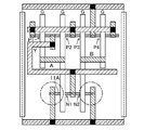
- FIG. 1 is a plan view showing a layout configuration example of a standard cell provided in the semiconductor integrated circuit device according to the first embodiment.
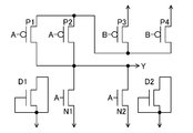
- FIG. 2 is a circuit diagram of the standard cell of FIG.
- the standard cell 1 in FIG. 1 is a cell that realizes a 2-input NOR circuit.
- a fin type transistor is constituted by a fin and a gate formed thereon.
- the local wiring is formed in contact with the upper layer of the fin or gate in a portion overlapping with the fin or gate in plan view, and is electrically connected.
- the metal wiring is located in an upper layer of the local wiring, and is connected to the local wiring through a contact.
- the fins are hatched for easy viewing. However, hatching is omitted for the portion located under the gate.
- the local wiring and the metal wiring are also hatched of different types, and the portion where the metal wiring and the local wiring are connected by a contact is shown in black. The same applies to other plan views.
- the standard cell 1 has fins 11 and 16 extending in the horizontal direction (first direction) in the drawing.
- the fin 11 is used to configure an N-type transistor in the N-type region
- the fin 16 is used to configure a P-type transistor in the P-type region. That is, the N-type transistor N1, which is an active transistor, is formed by the fin 11 and the gate wirings 12 and 13 provided on the fin 11 and extending in the vertical direction of the drawing (second direction perpendicular to the first direction).
- N2 is configured.
- N-type transistors N1 and N2 share a drain.
- the fins 16 and the gate wirings 17, 12, 13, 18 that extend in the vertical direction of the drawing and are provided on the fins 16 constitute P-type transistors P 1, P 2, P 3, P 4 that are active transistors, respectively. ing.
- a ground wiring 8a for supplying a ground potential is arranged at the lower end of the standard cell 1 so as to extend in the horizontal direction in the drawing.
- Dummy gate wirings 9a and 9b extending in the vertical direction of the drawing are arranged on the left and right ends of the standard cell 1, respectively.
- dummy transistors D1 and D2 are formed in the fin 11. That is, the dummy transistor D ⁇ b> 1 is configured by the fin 11 and the dummy gate wiring 14 provided on the fin 11 in parallel with the gate wiring 12.
- the N-type transistor N1 shares the source to which the ground potential as an example of the power supply potential is supplied with the dummy transistor D1.
- the dummy transistor D2 is configured by the fin 11 and the dummy gate wiring 15 provided on the fin 11 in parallel with the gate wiring 13.
- the N-type transistor N2 shares the source to which the ground potential is supplied with the dummy transistor D2.
- the dummy transistors D1 and D2 have their sources, drains, and gates all connected to a ground wiring 8a as an example of a power supply wiring.
- the N-type transistor N1 shares the source with the dummy transistor D1, and shares the drain with the N-type transistor N2 as the third transistor.
- the N-type transistor N2 shares the source with the dummy transistor D2, and shares the drain with the N-type transistor N1 as the third transistor. That is, in the layout configuration of FIG. 1, in the N-type region, all the active transistors N1, N2 share both source and drain nodes with other transistors.
- dummy transistors D1 and D2 are formed in the vicinity of the end portion of the fin 11, and the N-type transistors N1 and N2 which are active transistors are arranged at positions away from the vicinity of the end portion of the fin 11. ing. That is, the terminal portion of the fin 11 that has a high possibility of narrowing the fin width is removed from the arrangement position of the active transistors N1 and N2. As a result, it is possible to avoid the influence of the narrowing of the end of the fin 11 on the active transistors N1 and N2, and to suppress variation in performance of the active transistors N1 and N2, and to improve the electrical contact with the local wiring. Thus, it becomes possible to improve the yield of the semiconductor chip.
- FIG. 3 is a plan view showing a comparative example of the layout configuration of FIG.
- fins 11 ⁇ / b> A shorter than the fins 11 are arranged, and N-type transistors N ⁇ b> 1 and N ⁇ b> 2 are arranged in the vicinity of the terminal end portion (illustrated by a one-dot chain line). A dummy transistor is not formed.
- Dummy transistors D1 and D2 are unnecessary if only considering the logical function of the NOR circuit in FIG. Therefore, if the layout design is performed only in consideration of realizing the logic function of the NOR circuit in FIG. 2 and not considering the influence of the fin end portion thinning, the layout as shown in FIG. 3 without the dummy transistors D1 and D2 is provided. It is considered to be a composition.
- the use of the layout configuration of FIG. 3 increases the possibility that the performance of the semiconductor chip varies and the yield decreases.
- it is effective to use the layout configuration of FIG. 1 instead of the layout configuration of FIG.
- the effect of suppressing this variation is not limited to the cells constituting the clock tree, but is effective for other cells.
- the N-type transistor as the active transistor shares the source with the dummy transistor.
- the active transistor may share the drain with the dummy transistor.
- a P-type transistor as an active transistor may share a source or drain with a dummy transistor.
- the other source or drain node shared with the dummy transistor may be shared with another dummy transistor.
- the other source or drain node shared with the dummy transistor may not be shared with other transistors.
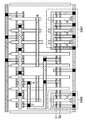
- FIG. 4 is a plan view showing a layout configuration example of a standard cell provided in the semiconductor integrated circuit device according to the second embodiment.
- the standard cell 2 shown in FIG. 4 is a cell that realizes the 2-input NOR circuit shown in FIG. 2, but each transistor shown in FIG. 2 is composed of two fins.
- the standard cell 2 has fins 11, 16, 21, and 22 that extend in the horizontal direction (first direction) of the drawing. Fins 11 and 21 are used to form an N-type transistor in the N-type region, and fins 16 and 22 are used to form a P-type transistor in the P-type region. That is, the N-type transistor N1, which is an active transistor, is formed by the fin 11 and the gate wirings 12 and 13 provided on the fin 11 and extending in the vertical direction of the drawing (second direction perpendicular to the first direction). N2 is configured.
- the fins 21 as the second fins and the gate wirings 12 and 13 extending on the fins 21 constitute N-type transistors N1a and N2a as the second active transistors, respectively.
- the fins 16 and the gate wirings 17, 12, 13, 18 that extend in the vertical direction of the drawing and are provided on the fins 16 constitute P-type transistors P 1, P 2, P 3, P 4 that are active transistors, respectively.
- P-type transistors P1a, P2a, P3a, and P4a are configured by the fin 22 and the gate wirings 17, 12, 13, and 18 extending on the fin 22, respectively.
- a ground wiring 8a for supplying a ground potential is arranged at the lower end of the standard cell 2 so as to extend in the horizontal direction in the drawing
- Dummy gate wirings 9a and 9b extending in the vertical direction of the drawing are arranged on the left and right ends of the standard cell 2, respectively.
- dummy transistors D1 and D2 are formed on the fin 11, and dummy transistors D1a and D2a are formed on the fin 21. That is, the dummy transistor D ⁇ b> 1 is configured by the fin 11 and the dummy gate wiring 14 provided on the fin 11 in parallel with the gate wiring 12.
- the dummy transistor D2 is configured by the fin 11 and the dummy gate wiring 15 provided on the fin 11 in parallel with the gate wiring 13.
- the N-type transistor N1 shares the source supplied with the ground potential with the dummy transistor D1, and the N-type transistor N2 shares the source supplied with the ground potential with the dummy transistor D2.
- the dummy transistor D1a is configured by the fin 21 and the dummy gate wiring 14 extending on the fin 21.
- the dummy transistor D2a is configured by the fin 21 and the dummy gate wiring 15 extending on the fin 21.
- the N-type transistor N1a shares the source supplied with the ground potential with the dummy transistor D1a
- the N-type transistor N2a shares the source supplied with the ground potential with the dummy transistor D2a.
- the dummy transistors D1, D2, D1a, and D2a have their sources, drains, and gates all connected to the ground wiring 8a.
- the N-type transistor N1 shares the source with the dummy transistor D1, and shares the drain with the N-type transistor N2.
- the N-type transistor N2 shares the source with the dummy transistor D2, and shares the drain with the N-type transistor N1.
- the N-type transistor N1a shares the source with the dummy transistor D1a and shares the drain with the N-type transistor N2a.
- the N-type transistor N2a shares the source with the dummy transistor D2a and shares the drain with the N-type transistor N1a. That is, in the layout configuration of FIG. 4, in the N-type region, all the active transistors N1, N2, N1a, and N1b share both source and drain nodes with other transistors.
- dummy transistors D1 and D2 are arranged in the vicinity of the end portion of the fin 11, and the N-type transistors N1 and N2 are arranged at positions away from the vicinity of the end portion of the fin 11. That is, the terminal portion of the fin 11 that has a high possibility of narrowing the fin width is removed from the arrangement position of the active transistors N1 and N2. Further, dummy transistors D1a and D2a are disposed in the vicinity of the end portion of the fin 21, and the N-type transistors N1a and N2a are disposed at positions away from the vicinity of the end portion of the fin 21. That is, the terminal portion of the fin 21 that is likely to have a narrow fin width is removed from the arrangement position of the active transistors N1a and N2a.
- FIG. 5 is a plan view showing a comparative example of the layout configuration of FIG.
- only one fin 11B is provided to form an N-type transistor, and N-type transistors N1a and N1b are arranged in the vicinity of the terminal portion (shown by a one-dot chain line). A dummy transistor is not formed.
- FIG. 2 When the NOR circuit (except for the dummy transistors D1 and D2) shown in FIG. 2 is formed with two fins for each transistor, if the layout is designed without considering the influence of the fin end portion, FIG. It is considered that the layout configuration is as follows.
- the use of the layout configuration of FIG. 5 increases the possibility that the performance of the semiconductor chip varies and the yield decreases.
- a cell constituting a clock tree that propagates a clock signal it is necessary to suppress variation in performance. Therefore, it is effective to use the layout configuration of FIG. 4 instead of the layout configuration of FIG.
- the effect of suppressing this variation is not limited to the cells constituting the clock tree, but is effective for other cells.
- FIG. 6 is a plan view showing another layout configuration example of the standard cell in the present embodiment.
- the standard cell 2A of FIG. 6 implements the same circuit configuration as that of FIG. 4, but the N-type transistors N1, N2, N1a, and N1b share the drain with the dummy transistors D1, D2, D1a, and D2a, respectively. is doing.
- the sources and gates of the dummy transistors D1, D2, D1a, D2a are connected to the ground wiring 8a.
- the end portions of the fins 11 and 21 that are likely to have a narrow fin width are removed from the arrangement positions of the active transistors N1, N2, N1a, and N2a. .
- the end portions of the fins 11 and 21 that are likely to have a narrow fin width are removed from the arrangement positions of the active transistors N1, N2, N1a, and N2a.
- the influence of the narrowing of the end of the fin 11 on the active transistors N1 and N2 and the influence of the thinning of the end of the fin 21 on the active transistors N1a and N1b, and the active transistors N1, N2, N1a, and N1b. It is possible to suppress variations in performance.
- FIG. 7 is a plan view showing another layout configuration example of the standard cell in the present embodiment.
- the standard cell 2B in FIG. 7 realizes the same circuit configuration as that in FIG. 4, but the N-type transistors N1, N2, N1a, and N1b share both the drain and the source with the dummy transistors. . Further, the P-type transistors P1, P4, P1a, and P4a share the drain with the dummy transistor, respectively.
- the fins 31 and 32 and the dummy gate wiring 33 constitute a dummy transistor sharing the source with the N-type transistors N1 and N1a.
- the fins 31 and 32 and the dummy gate wiring 34 form a dummy transistor sharing the drain with the N-type transistors N1 and N1a, and the fins 31 and 32 and the dummy gate wiring 35 A dummy transistor sharing the drain with the n-type transistors N2 and N2a is configured.
- the fins 31 and 32 and the dummy gate wiring 36 constitute a dummy transistor sharing the source with the N-type transistors N2 and N2a.
- the dummy transistors that share the drain with the P-type transistors P1 and P1a are constituted by the fins 37 and 38 and the dummy gate wiring 39.
- the fins 37 and 38 and the dummy gate wiring 40 constitute a dummy transistor sharing the drain with the P-type transistors P4 and P4a.
- FIG. 8 is a plan view showing another layout configuration example of the standard cell in the embodiment
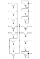
- FIG. 9 is a circuit diagram of the standard cell of FIG.
- each transistor of FIG. 9 is configured by two fins.
- dummy transistors are formed at the end portions of the fins 41 and 42.
- a dummy transistor is configured by the fins 41 and 42 and the dummy gate wirings 43 and 44.
- a dummy transistor is formed by the fins 41 and 42 and the dummy gate wirings 45 and 46.
- FIG. 10 is a plan view showing another layout configuration example of the standard cell in the embodiment
- FIG. 11 is a circuit diagram of the standard cell of FIG.
- each transistor of FIG. 11 is configured by two fins.
- dummy transistors are formed at the end portions of the fins 51 and 52.
- a dummy transistor is configured by the fins 51 and 52 and the dummy gate wiring 53.
- a dummy transistor is formed by the fins 51, 52 and the dummy gate wirings 54, 55, 56.
- the NOR circuit has been described as an example.
- the present disclosure is not limited to this, and the present disclosure is also applicable to, for example, a semiconductor integrated circuit device that realizes other logic functions such as an inverter, a NAND, and a flip-flop. The same applies.
- the ground potential is applied to the gate to fix the gate potential.
- the present invention is not limited to this, and other functions that do not contribute to the logic function are provided.
- a configuration may be adopted.
- a power supply potential may be applied to the gate and a ground potential may be applied to the source / drain.
Landscapes
- Semiconductor Integrated Circuits (AREA)
- Design And Manufacture Of Integrated Circuits (AREA)
- Physics & Mathematics (AREA)
- Geometry (AREA)
- Engineering & Computer Science (AREA)
- General Engineering & Computer Science (AREA)
- Metal-Oxide And Bipolar Metal-Oxide Semiconductor Integrated Circuits (AREA)
Abstract
Description
図1は第1の実施形態に係る半導体集積回路装置が備えたスタンダードセルのレイアウト構成例を示す平面図である。また図2は図1のスタンダードセルの回路図である。図2に示すとおり、図1のスタンダードセル1は2入力のNOR回路を実現するセルである。図1および他の平面図では、フィンとその上に形成されたゲートとによって、フィン型トランジスタが構成されている。ローカル配線は、平面視でフィンまたはゲートと重なる部分において、フィンまたはゲートの上層に接して形成されており、電気的に接続されている。メタル配線はローカル配線の上層に位置しており、コンタクトを介してローカル配線と接続されている。なお、図1では図の見やすさのために、フィンにハッチを付している。ただし、ゲートの下に位置する部分についてはハッチを省いている。また、ローカル配線およびメタル配線にも種類が異なるハッチを付しており、メタル配線とローカル配線とがコンタクトで接続された部分を黒く塗りつぶして示している。他の平面図においても同様である。
図4は第2の実施形態に係る半導体集積回路装置が備えたスタンダードセルのレイアウト構成例を示す平面図である。図4のスタンダードセル2は、図2に示す2入力のNOR回路を実現するセルであるが、図2の各トランジスタがそれぞれ2枚のフィンで構成されている。
図8は実施形態におけるスタンダードセルの他のレイアウト構成例を示す平面図、図9は図8のスタンダードセルの回路図である。ただし図8では、図9の各トランジスタがそれぞれ2枚のフィンで構成されている。図8のレイアウト構成では、フィン41,42の終端部にダミートランジスタが形成されている。図面左側における領域DN4では、フィン41,42とダミーゲート配線43,44とによって、ダミートランジスタが構成されている。図面右側における領域DN5では、フィン41,42とダミーゲート配線45,46とによって、ダミートランジスタが形成されている。
8a 接地配線(電源配線)
11 フィン
12,13 ゲート配線
14,15 ダミーゲート配線
16,22 フィン
21 フィン(第2フィン)
31,32,37,38 フィン
33,34,35,36,39,40 ダミーゲート配線
41,42 フィン
43,44,45,46 ダミーゲート配線
51,52 フィン
53,54,55,56 ダミーゲート配線
N1,N2,N1a,N2a アクティブトランジスタ
D1,D2,D1a,D2a ダミートランジスタ
Claims (11)
- 第1方向に延びるフィンを有するスタンダードセルを備え、
前記スタンダードセルは、
前記フィンと、前記第1方向と垂直をなす第2方向に延びており、前記フィン上に設けられたゲート配線とによって構成されたアクティブトランジスタと、
前記フィンと、前記ゲート配線と並列に、前記フィン上に設けられたダミーゲート配線とによって構成され、前記アクティブトランジスタとソースまたはドレインの一方のノードを共有しているダミートランジスタとを備えている
ことを特徴とする半導体集積回路装置。 - 請求項1記載の半導体集積回路装置において、
前記スタンダードセルは、
前記フィンと、前記ゲート配線と並列にかつ前記ダミーゲート配線と反対側に、前記フィン上に設けられた第2ゲート配線とによって構成され、前記アクティブトランジスタとソースまたはドレインの他方のノードを共有している第3トランジスタを備えている
ことを特徴とする半導体集積回路装置。 - 請求項2記載の半導体集積回路装置において、
前記第3トランジスタは、アクティブトランジスタである
ことを特徴とする半導体集積回路装置。 - 請求項2記載の半導体集積回路装置において、
前記第3トランジスタは、ダミートランジスタである
ことを特徴とする半導体集積回路装置。 - 請求項1記載の半導体集積回路装置において、
前記アクティブトランジスタが前記ダミートランジスタと共有しているノードは、電源電位が供給されるソースである
ことを特徴とする半導体集積回路装置。 - 請求項5記載の半導体集積回路装置において、
前記ダミートランジスタは、ソース、ドレインおよびゲートがいずれも電源配線に接続されている
ことを特徴とする半導体集積回路装置。 - 請求項1記載の半導体集積回路装置において、
前記アクティブトランジスタが前記ダミートランジスタと共有しているノードは、ドレインであり、前記ダミートランジスタは、ソースおよびゲートが電源配線に接続されている
ことを特徴とする半導体集積回路装置。 - 請求項1記載の半導体集積回路装置において、
前記スタンダードセルは、
前記フィンが形成された第1導電型領域において、前記フィンと並列に配置された第2フィンを有し、
前記ゲート配線および前記ダミーゲート配線は、前記第2フィン上まで延びており、
前記第2フィンと前記ゲート配線とによって構成された第2アクティブトランジスタと、
前記第2フィンと前記ダミーゲート配線とによって構成され、前記第2アクティブトランジスタとソースまたはドレインの一方のノードを共有している第2ダミートランジスタとを備えている
ことを特徴とする半導体集積回路装置。 - 請求項1記載の半導体集積回路装置において、
前記スタンダードセルは、
前記フィンが形成された第1導電型領域において、全てのアクティブトランジスタは、ソースおよびドレインの両方のノードを他のトランジスタと共有している
ことを特徴とする半導体集積回路装置。 - 請求項9記載の半導体集積回路装置において、
前記スタンダードセルにおいて、全てのアクティブトランジスタは、ソースおよびドレインの両方のノードを他のトランジスタと共有している
ことを特徴とする半導体集積回路装置。 - 請求項1記載の半導体集積回路装置において、
前記スタンダードセルは、クロックツリーを構成するセルである
ことを特徴とする半導体集積回路装置。
Priority Applications (9)
| Application Number | Priority Date | Filing Date | Title |
|---|---|---|---|
| JP2015532681A JP6281570B2 (ja) | 2013-08-23 | 2014-04-21 | 半導体集積回路装置 |
| CN201480046450.2A CN105493264B (zh) | 2013-08-23 | 2014-04-21 | 半导体集成电路装置 |
| CN201810440111.2A CN108630607B (zh) | 2013-08-23 | 2014-04-21 | 半导体集成电路装置 |
| US15/049,680 US9899381B2 (en) | 2013-08-23 | 2016-02-22 | Semiconductor integrated circuit device having a standard cell which includes a fin |
| US15/863,107 US10181469B2 (en) | 2013-08-23 | 2018-01-05 | Semiconductor integrated circuit device having a standard cell which includes a fin |
| US16/211,919 US10833075B2 (en) | 2013-08-23 | 2018-12-06 | Semiconductor integrated circuit device having a standard cell which includes a fin |
| US17/039,051 US11362088B2 (en) | 2013-08-23 | 2020-09-30 | Semiconductor integrated circuit device having a standard cell which includes a fin and a dummy transistor |
| US17/744,141 US11764217B2 (en) | 2013-08-23 | 2022-05-13 | Semiconductor integrated circuit device having a standard cell which includes a fin and a dummy transistor |
| US18/450,146 US12094878B2 (en) | 2013-08-23 | 2023-08-15 | Semiconductor integrated circuit device having a standard cell which includes a fin and a dummy transistor |
Applications Claiming Priority (2)
| Application Number | Priority Date | Filing Date | Title |
|---|---|---|---|
| JP2013-173739 | 2013-08-23 | ||
| JP2013173739 | 2013-08-23 |
Related Child Applications (1)
| Application Number | Title | Priority Date | Filing Date |
|---|---|---|---|
| US15/049,680 Continuation US9899381B2 (en) | 2013-08-23 | 2016-02-22 | Semiconductor integrated circuit device having a standard cell which includes a fin |
Publications (1)
| Publication Number | Publication Date |
|---|---|
| WO2015025441A1 true WO2015025441A1 (ja) | 2015-02-26 |
Family
ID=52483241
Family Applications (1)
| Application Number | Title | Priority Date | Filing Date |
|---|---|---|---|
| PCT/JP2014/002237 Ceased WO2015025441A1 (ja) | 2013-08-23 | 2014-04-21 | 半導体集積回路装置 |
Country Status (4)
| Country | Link |
|---|---|
| US (6) | US9899381B2 (ja) |
| JP (2) | JP6281570B2 (ja) |
| CN (2) | CN108630607B (ja) |
| WO (1) | WO2015025441A1 (ja) |
Cited By (10)
| Publication number | Priority date | Publication date | Assignee | Title |
|---|---|---|---|---|
| WO2016154405A1 (en) * | 2015-03-25 | 2016-09-29 | Qualcomm Incorporated | Finfet device for n/p tuning |
| JP2018530155A (ja) * | 2015-09-24 | 2018-10-11 | クゥアルコム・インコーポレイテッドQualcomm Incorporated | ソース分離型セル |
| WO2019116883A1 (ja) * | 2017-12-12 | 2019-06-20 | 株式会社ソシオネクスト | 半導体集積回路装置 |
| JP2019530229A (ja) * | 2016-09-20 | 2019-10-17 | クアルコム,インコーポレイテッド | 20nm未満のフィンピッチのための新規の自己整合4重パターニングプロセス |
| JP2019201228A (ja) * | 2013-09-04 | 2019-11-21 | 株式会社ソシオネクスト | 半導体装置 |
| JP2019216289A (ja) * | 2019-10-01 | 2019-12-19 | ルネサスエレクトロニクス株式会社 | 半導体装置 |
| WO2020170715A1 (ja) * | 2019-02-18 | 2020-08-27 | 株式会社ソシオネクスト | 半導体集積回路装置 |
| JPWO2020137746A1 (ja) * | 2018-12-26 | 2021-11-18 | 株式会社ソシオネクスト | 半導体集積回路装置 |
| JP2022101634A (ja) * | 2017-11-21 | 2022-07-06 | アドバンスト・マイクロ・ディバイシズ・インコーポレイテッド | セル面積を縮小し、チップレベルでのセル配置を改善するための金属0電源接地スタブ経路(metal zero power ground stub route) |
| JP2023071757A (ja) * | 2017-05-01 | 2023-05-23 | アドバンスト・マイクロ・ディバイシズ・インコーポレイテッド | 標準セルレイアウトアーキテクチャ及び5nm以降の描画スタイル |
Families Citing this family (23)
| Publication number | Priority date | Publication date | Assignee | Title |
|---|---|---|---|---|
| WO2015025441A1 (ja) | 2013-08-23 | 2015-02-26 | パナソニック株式会社 | 半導体集積回路装置 |
| JP6396834B2 (ja) | 2015-03-23 | 2018-09-26 | ルネサスエレクトロニクス株式会社 | 半導体装置 |
| US9793211B2 (en) * | 2015-10-20 | 2017-10-17 | Taiwan Semiconductor Manufacturing Co., Ltd. | Dual power structure with connection pins |
| JP6823270B2 (ja) * | 2016-06-28 | 2021-02-03 | 株式会社ソシオネクスト | 半導体装置及び半導体集積回路 |
| CN109314080B (zh) * | 2016-07-01 | 2022-09-30 | 株式会社索思未来 | 半导体集成电路装置 |
| CN116886076A (zh) * | 2016-07-14 | 2023-10-13 | 三星电子株式会社 | 包括三态反相器的触发器 |
| CN109564893B (zh) * | 2016-08-01 | 2022-11-25 | 株式会社索思未来 | 半导体芯片 |
| KR102633141B1 (ko) * | 2016-12-07 | 2024-02-02 | 삼성전자주식회사 | 집적회로 소자 |
| KR102568562B1 (ko) * | 2017-01-24 | 2023-08-18 | 삼성전자주식회사 | 반도체 장치 |
| WO2019043888A1 (ja) * | 2017-08-31 | 2019-03-07 | 株式会社ソシオネクスト | 半導体集積回路装置 |
| CN109524394B (zh) * | 2017-09-18 | 2021-08-10 | 联华电子股份有限公司 | 具有虚置标准单元的集成电路 |
| KR102362016B1 (ko) | 2017-09-19 | 2022-02-10 | 삼성전자주식회사 | 마스터 슬레이브 플립 플롭 |
| TWI756405B (zh) * | 2018-04-13 | 2022-03-01 | 聯華電子股份有限公司 | 靜態隨機存取記憶體的信噪比的調整方式以及反相器的結構 |
| TWI762425B (zh) * | 2018-04-13 | 2022-04-21 | 聯華電子股份有限公司 | 靜態隨機存取記憶體的信噪比的調整方式以及反相器的結構 |
| CN110600546B (zh) * | 2018-06-13 | 2022-12-06 | 联华电子股份有限公司 | 纳米管晶体管结构和纳米管反相器结构 |
| US11094695B2 (en) * | 2019-05-17 | 2021-08-17 | Taiwan Semiconductor Manufacturing Co., Ltd. | Integrated circuit device and method of forming the same |
| JP7302658B2 (ja) | 2019-06-18 | 2023-07-04 | 株式会社ソシオネクスト | 半導体装置 |
| US11810920B2 (en) * | 2019-11-29 | 2023-11-07 | Samsung Electronics Co., Ltd. | Integrated circuits including integrated standard cell structure |
| US11557590B2 (en) * | 2020-02-19 | 2023-01-17 | Taiwan Semiconductor Manufacturing Co., Ltd. | Transistor gate profile optimization |
| DE102020116347B4 (de) | 2020-02-19 | 2025-03-13 | Taiwan Semiconductor Manufacturing Co., Ltd. | Vorrichtung und optimierung eines transistor-gate-profils |
| US11222831B2 (en) * | 2020-06-04 | 2022-01-11 | Samsung Electronics Co., Ltd. | Stacked integrated circuit devices |
| KR102747647B1 (ko) | 2020-09-10 | 2024-12-27 | 삼성전자주식회사 | 집적회로 장치 |
| KR102932765B1 (ko) * | 2021-09-27 | 2026-03-05 | 삼성전자주식회사 | 반도체 장치 |
Citations (6)
| Publication number | Priority date | Publication date | Assignee | Title |
|---|---|---|---|---|
| JPH09289251A (ja) * | 1996-04-23 | 1997-11-04 | Matsushita Electric Ind Co Ltd | 半導体集積回路のレイアウト構造およびその検証方法 |
| JP2007012855A (ja) * | 2005-06-30 | 2007-01-18 | Matsushita Electric Ind Co Ltd | 半導体集積回路、標準セル、標準セルライブラリ、半導体集積回路の設計方法および半導体集積回路の設計装置 |
| JP2009218499A (ja) * | 2008-03-12 | 2009-09-24 | Sony Corp | 半導体装置 |
| JP2010016258A (ja) * | 2008-07-04 | 2010-01-21 | Panasonic Corp | 半導体集積回路装置 |
| JP2010021469A (ja) * | 2008-07-14 | 2010-01-28 | Nec Electronics Corp | 半導体集積回路 |
| JP2010123947A (ja) * | 2008-11-21 | 2010-06-03 | Taiwan Semiconductor Manufacturing Co Ltd | 性能を改善する新しいレイアウト構造 |
Family Cites Families (43)
| Publication number | Priority date | Publication date | Assignee | Title |
|---|---|---|---|---|
| US6399972B1 (en) * | 2000-03-13 | 2002-06-04 | Oki Electric Industry Co., Ltd. | Cell based integrated circuit and unit cell architecture therefor |
| JP2002353413A (ja) * | 2001-05-28 | 2002-12-06 | Mitsubishi Electric Corp | 半導体記憶装置 |
| JP2005116969A (ja) * | 2003-10-10 | 2005-04-28 | Toshiba Corp | 半導体装置及びその製造方法 |
| KR100702552B1 (ko) | 2003-12-22 | 2007-04-04 | 인터내셔널 비지네스 머신즈 코포레이션 | 이중 게이트 FinFET 디자인을 위한 자동화 레이어생성 방법 및 장치 |
| JP4829645B2 (ja) * | 2006-03-08 | 2011-12-07 | パナソニック株式会社 | 半導体集積回路装置 |
| US9009641B2 (en) | 2006-03-09 | 2015-04-14 | Tela Innovations, Inc. | Circuits with linear finfet structures |
| US9563733B2 (en) | 2009-05-06 | 2017-02-07 | Tela Innovations, Inc. | Cell circuit and layout with linear finfet structures |
| US7446352B2 (en) * | 2006-03-09 | 2008-11-04 | Tela Innovations, Inc. | Dynamic array architecture |
| US7812373B2 (en) * | 2007-02-12 | 2010-10-12 | Infineon Technologies Ag | MuGFET array layout |
| US8518767B2 (en) | 2007-02-28 | 2013-08-27 | International Business Machines Corporation | FinFET with reduced gate to fin overlay sensitivity |
| US8682116B2 (en) * | 2007-08-08 | 2014-03-25 | Infineon Technologies Ag | Integrated circuit including non-planar structure and waveguide |
| US20110018064A1 (en) * | 2008-04-04 | 2011-01-27 | Nxp B.V. | Sram cell comprising finfets |
| US8004042B2 (en) * | 2009-03-20 | 2011-08-23 | Taiwan Semiconductor Manufacturing Company, Ltd. | Static random access memory (SRAM) cell and method for forming same |
| JPWO2010122754A1 (ja) * | 2009-04-22 | 2012-10-25 | パナソニック株式会社 | 半導体集積回路 |
| US8216902B2 (en) * | 2009-08-06 | 2012-07-10 | International Business Machines Corporation | Nanomesh SRAM cell |
| JP5531848B2 (ja) * | 2010-08-06 | 2014-06-25 | 富士通セミコンダクター株式会社 | 半導体装置、半導体集積回路装置、SRAM、Dt−MOSトランジスタの製造方法 |
| US8848423B2 (en) * | 2011-02-14 | 2014-09-30 | Shine C. Chung | Circuit and system of using FinFET for building programmable resistive devices |
| US8816444B2 (en) * | 2011-04-29 | 2014-08-26 | Taiwan Semiconductor Manufacturing Company, Ltd. | System and methods for converting planar design to FinFET design |
| KR101850703B1 (ko) * | 2011-05-17 | 2018-04-23 | 삼성전자 주식회사 | 반도체 장치 및 그 제조 방법 |
| US8519462B2 (en) * | 2011-06-27 | 2013-08-27 | Intel Corporation | 6F2 DRAM cell |
| JP2013030602A (ja) * | 2011-07-28 | 2013-02-07 | Panasonic Corp | 半導体集積回路装置 |
| US8561003B2 (en) * | 2011-07-29 | 2013-10-15 | Synopsys, Inc. | N-channel and P-channel finFET cell architecture with inter-block insulator |
| EP2803077A4 (en) | 2012-01-13 | 2015-11-04 | Tela Innovations Inc | CIRCUITS WITH LINEAR FINFET STRUCTURES |
| US9196540B2 (en) * | 2012-02-07 | 2015-11-24 | Taiwan Semiconductor Manufacturing Company, Ltd. | FinFET structure with novel edge fins |
| US8723268B2 (en) * | 2012-06-13 | 2014-05-13 | Synopsys, Inc. | N-channel and P-channel end-to-end finFET cell architecture with relaxed gate pitch |
| US8901615B2 (en) * | 2012-06-13 | 2014-12-02 | Synopsys, Inc. | N-channel and P-channel end-to-end finfet cell architecture |
| US8766364B2 (en) | 2012-08-31 | 2014-07-01 | Taiwan Semiconductor Manufacturing Company, Ltd. | Fin field effect transistor layout for stress optimization |
| US9576978B2 (en) | 2012-10-09 | 2017-02-21 | Samsung Electronics Co., Ltd. | Cells including at least one fin field effect transistor and semiconductor integrated circuits including the same |
| US9093304B2 (en) * | 2012-10-12 | 2015-07-28 | Finscale Inc. | Vertical super-thin body semiconductor on dielectric wall devices and methods of their fabrication |
| US9337318B2 (en) * | 2012-10-26 | 2016-05-10 | Taiwan Semiconductor Manufacturing Company, Ltd. | FinFET with dummy gate on non-recessed shallow trench isolation (STI) |
| US9012287B2 (en) * | 2012-11-14 | 2015-04-21 | Taiwan Semiconductor Manufacturing Company, Ltd. | Cell layout for SRAM FinFET transistors |
| US9059242B2 (en) * | 2012-11-27 | 2015-06-16 | International Business Machines Corporation | FinFET semiconductor device having increased gate height control |
| US9064725B2 (en) * | 2012-12-14 | 2015-06-23 | Taiwan Semiconductor Manufacturing Company, Ltd. | FinFET with embedded MOS varactor and method of making same |
| US8739104B1 (en) * | 2013-02-28 | 2014-05-27 | Broadcom Corporation | Systems and methods for forming an integrated circuit using a standard cell library |
| US9318621B2 (en) * | 2013-03-08 | 2016-04-19 | Taiwan Semiconductor Manufacturing Company, Ltd. | Rotated STI diode on FinFET technology |
| US8869090B2 (en) | 2013-03-11 | 2014-10-21 | Taiwan Semiconductor Manufacturing Company, Ltd. | Stretch dummy cell insertion in FinFET process |
| US9997617B2 (en) * | 2013-03-13 | 2018-06-12 | Qualcomm Incorporated | Metal oxide semiconductor (MOS) isolation schemes with continuous active areas separated by dummy gates and related methods |
| US9111801B2 (en) * | 2013-04-04 | 2015-08-18 | Stmicroelectronics, Inc. | Integrated circuit devices and fabrication techniques |
| US9158877B2 (en) | 2013-05-02 | 2015-10-13 | Taiwan Semiconductor Manufacturing Company, Ltd. | Standard cell metal structure directly over polysilicon structure |
| US20150008524A1 (en) * | 2013-07-02 | 2015-01-08 | United Microelectronics Corp. | Integrated circuit device structure and fabrication method thereof |
| US9536876B2 (en) * | 2013-08-01 | 2017-01-03 | Taiwan Semiconductor Manufacturing Company Ltd. | Temperature detector and controlling heat |
| US9219153B2 (en) * | 2013-08-21 | 2015-12-22 | Globalfoundries Inc. | Methods of forming gate structures for FinFET devices and the resulting semiconductor products |
| WO2015025441A1 (ja) * | 2013-08-23 | 2015-02-26 | パナソニック株式会社 | 半導体集積回路装置 |
-
2014
- 2014-04-21 WO PCT/JP2014/002237 patent/WO2015025441A1/ja not_active Ceased
- 2014-04-21 CN CN201810440111.2A patent/CN108630607B/zh active Active
- 2014-04-21 CN CN201480046450.2A patent/CN105493264B/zh active Active
- 2014-04-21 JP JP2015532681A patent/JP6281570B2/ja active Active
-
2016
- 2016-02-22 US US15/049,680 patent/US9899381B2/en active Active
-
2018
- 2018-01-05 US US15/863,107 patent/US10181469B2/en active Active
- 2018-01-25 JP JP2018010604A patent/JP2018064125A/ja active Pending
- 2018-12-06 US US16/211,919 patent/US10833075B2/en active Active
-
2020
- 2020-09-30 US US17/039,051 patent/US11362088B2/en active Active
-
2022
- 2022-05-13 US US17/744,141 patent/US11764217B2/en active Active
-
2023
- 2023-08-15 US US18/450,146 patent/US12094878B2/en active Active
Patent Citations (6)
| Publication number | Priority date | Publication date | Assignee | Title |
|---|---|---|---|---|
| JPH09289251A (ja) * | 1996-04-23 | 1997-11-04 | Matsushita Electric Ind Co Ltd | 半導体集積回路のレイアウト構造およびその検証方法 |
| JP2007012855A (ja) * | 2005-06-30 | 2007-01-18 | Matsushita Electric Ind Co Ltd | 半導体集積回路、標準セル、標準セルライブラリ、半導体集積回路の設計方法および半導体集積回路の設計装置 |
| JP2009218499A (ja) * | 2008-03-12 | 2009-09-24 | Sony Corp | 半導体装置 |
| JP2010016258A (ja) * | 2008-07-04 | 2010-01-21 | Panasonic Corp | 半導体集積回路装置 |
| JP2010021469A (ja) * | 2008-07-14 | 2010-01-28 | Nec Electronics Corp | 半導体集積回路 |
| JP2010123947A (ja) * | 2008-11-21 | 2010-06-03 | Taiwan Semiconductor Manufacturing Co Ltd | 性能を改善する新しいレイアウト構造 |
Cited By (22)
| Publication number | Priority date | Publication date | Assignee | Title |
|---|---|---|---|---|
| JP2019201228A (ja) * | 2013-09-04 | 2019-11-21 | 株式会社ソシオネクスト | 半導体装置 |
| CN107408556A (zh) * | 2015-03-25 | 2017-11-28 | 高通股份有限公司 | 用于n/p调谐的鳍式fet器件 |
| US9978738B2 (en) | 2015-03-25 | 2018-05-22 | Qualcomm Incorporated | System, apparatus, and method for N/P tuning in a fin-FET |
| WO2016154405A1 (en) * | 2015-03-25 | 2016-09-29 | Qualcomm Incorporated | Finfet device for n/p tuning |
| JP2018530155A (ja) * | 2015-09-24 | 2018-10-11 | クゥアルコム・インコーポレイテッドQualcomm Incorporated | ソース分離型セル |
| JP2019530229A (ja) * | 2016-09-20 | 2019-10-17 | クアルコム,インコーポレイテッド | 20nm未満のフィンピッチのための新規の自己整合4重パターニングプロセス |
| JP2023071757A (ja) * | 2017-05-01 | 2023-05-23 | アドバンスト・マイクロ・ディバイシズ・インコーポレイテッド | 標準セルレイアウトアーキテクチャ及び5nm以降の描画スタイル |
| JP7809663B2 (ja) | 2017-05-01 | 2026-02-02 | アドバンスト・マイクロ・ディバイシズ・インコーポレイテッド | 標準セルレイアウトアーキテクチャ及び5nm以降の描画スタイル |
| US12455999B2 (en) | 2017-11-21 | 2025-10-28 | Advanced Micro Devices, Inc. | Metal zero power ground stub route to reduce cell area and improve cell placement at the chip level |
| JP7668763B2 (ja) | 2017-11-21 | 2025-04-25 | アドバンスト・マイクロ・ディバイシズ・インコーポレイテッド | セル面積を縮小し、チップレベルでのセル配置を改善するための金属0電源接地スタブ経路(metal zero power ground stub route) |
| JP2022101634A (ja) * | 2017-11-21 | 2022-07-06 | アドバンスト・マイクロ・ディバイシズ・インコーポレイテッド | セル面積を縮小し、チップレベルでのセル配置を改善するための金属0電源接地スタブ経路(metal zero power ground stub route) |
| WO2019116883A1 (ja) * | 2017-12-12 | 2019-06-20 | 株式会社ソシオネクスト | 半導体集積回路装置 |
| JPWO2019116883A1 (ja) * | 2017-12-12 | 2020-12-03 | 株式会社ソシオネクスト | 半導体集積回路装置 |
| US11342412B2 (en) | 2017-12-12 | 2022-05-24 | Socionext Inc. | Semiconductor integrated circuit device |
| JP7174263B2 (ja) | 2017-12-12 | 2022-11-17 | 株式会社ソシオネクスト | 半導体集積回路装置 |
| JPWO2020137746A1 (ja) * | 2018-12-26 | 2021-11-18 | 株式会社ソシオネクスト | 半導体集積回路装置 |
| JP7364922B2 (ja) | 2018-12-26 | 2023-10-19 | 株式会社ソシオネクスト | 半導体集積回路装置 |
| JP7364928B2 (ja) | 2019-02-18 | 2023-10-19 | 株式会社ソシオネクスト | 半導体集積回路装置 |
| US12119349B2 (en) | 2019-02-18 | 2024-10-15 | Socionext Inc. | Semiconductor integrated circuit device |
| JPWO2020170715A1 (ja) * | 2019-02-18 | 2021-12-23 | 株式会社ソシオネクスト | 半導体集積回路装置 |
| WO2020170715A1 (ja) * | 2019-02-18 | 2020-08-27 | 株式会社ソシオネクスト | 半導体集積回路装置 |
| JP2019216289A (ja) * | 2019-10-01 | 2019-12-19 | ルネサスエレクトロニクス株式会社 | 半導体装置 |
Also Published As
| Publication number | Publication date |
|---|---|
| US9899381B2 (en) | 2018-02-20 |
| CN108630607B (zh) | 2022-04-26 |
| US20190109133A1 (en) | 2019-04-11 |
| US20180130799A1 (en) | 2018-05-10 |
| JPWO2015025441A1 (ja) | 2017-03-02 |
| CN105493264B (zh) | 2018-06-01 |
| JP2018064125A (ja) | 2018-04-19 |
| US11362088B2 (en) | 2022-06-14 |
| US10833075B2 (en) | 2020-11-10 |
| JP6281570B2 (ja) | 2018-02-21 |
| US20220278096A1 (en) | 2022-09-01 |
| CN105493264A (zh) | 2016-04-13 |
| US20210013201A1 (en) | 2021-01-14 |
| US20230387116A1 (en) | 2023-11-30 |
| CN108630607A (zh) | 2018-10-09 |
| US20160172360A1 (en) | 2016-06-16 |
| US10181469B2 (en) | 2019-01-15 |
| US12094878B2 (en) | 2024-09-17 |
| US11764217B2 (en) | 2023-09-19 |
Similar Documents
| Publication | Publication Date | Title |
|---|---|---|
| JP6281570B2 (ja) | 半導体集積回路装置 | |
| US11784188B2 (en) | Semiconductor integrated circuit device | |
| JP6579205B2 (ja) | 半導体装置 | |
| US12237266B2 (en) | Semiconductor integrated circuit device | |
| CN109616445B (zh) | 半导体集成电路及逻辑电路 | |
| CN101339947A (zh) | 半导体器件 | |
| WO2015029280A1 (ja) | 半導体集積回路装置 | |
| WO2020095765A1 (ja) | 半導体集積回路装置 | |
| CN110326099B (zh) | 半导体集成电路装置 | |
| TW201921682A (zh) | 在採用高密度金屬佈線中之高效能電池設計 |
Legal Events
| Date | Code | Title | Description |
|---|---|---|---|
| WWE | Wipo information: entry into national phase |
Ref document number: 201480046450.2 Country of ref document: CN |
|
| 121 | Ep: the epo has been informed by wipo that ep was designated in this application |
Ref document number: 14837883 Country of ref document: EP Kind code of ref document: A1 |
|
| ENP | Entry into the national phase |
Ref document number: 2015532681 Country of ref document: JP Kind code of ref document: A |
|
| NENP | Non-entry into the national phase |
Ref country code: DE |
|
| 122 | Ep: pct application non-entry in european phase |
Ref document number: 14837883 Country of ref document: EP Kind code of ref document: A1 |