WO2015022875A1 - Printed circuit board inspection device - Google Patents
Printed circuit board inspection device Download PDFInfo
- Publication number
- WO2015022875A1 WO2015022875A1 PCT/JP2014/070549 JP2014070549W WO2015022875A1 WO 2015022875 A1 WO2015022875 A1 WO 2015022875A1 JP 2014070549 W JP2014070549 W JP 2014070549W WO 2015022875 A1 WO2015022875 A1 WO 2015022875A1
- Authority
- WO
- WIPO (PCT)
- Prior art keywords
- inspection
- printed circuit
- circuit board
- tray
- unit
- Prior art date
Links
Images


Classifications
-
- H—ELECTRICITY
- H05—ELECTRIC TECHNIQUES NOT OTHERWISE PROVIDED FOR
- H05K—PRINTED CIRCUITS; CASINGS OR CONSTRUCTIONAL DETAILS OF ELECTRIC APPARATUS; MANUFACTURE OF ASSEMBLAGES OF ELECTRICAL COMPONENTS
- H05K1/00—Printed circuits
- H05K1/02—Details
- H05K1/0266—Marks, test patterns or identification means
- H05K1/0268—Marks, test patterns or identification means for electrical inspection or testing
-
- G—PHYSICS
- G01—MEASURING; TESTING
- G01R—MEASURING ELECTRIC VARIABLES; MEASURING MAGNETIC VARIABLES
- G01R31/00—Arrangements for testing electric properties; Arrangements for locating electric faults; Arrangements for electrical testing characterised by what is being tested not provided for elsewhere
- G01R31/28—Testing of electronic circuits, e.g. by signal tracer
- G01R31/2801—Testing of printed circuits, backplanes, motherboards, hybrid circuits or carriers for multichip packages [MCP]
- G01R31/2806—Apparatus therefor, e.g. test stations, drivers, analysers, conveyors
- G01R31/2808—Holding, conveying or contacting devices, e.g. test adapters, edge connectors, extender boards
-
- G—PHYSICS
- G01—MEASURING; TESTING
- G01R—MEASURING ELECTRIC VARIABLES; MEASURING MAGNETIC VARIABLES
- G01R31/00—Arrangements for testing electric properties; Arrangements for locating electric faults; Arrangements for electrical testing characterised by what is being tested not provided for elsewhere
- G01R31/28—Testing of electronic circuits, e.g. by signal tracer
- G01R31/2801—Testing of printed circuits, backplanes, motherboards, hybrid circuits or carriers for multichip packages [MCP]
- G01R31/281—Specific types of tests or tests for a specific type of fault, e.g. thermal mapping, shorts testing
- G01R31/2812—Checking for open circuits or shorts, e.g. solder bridges; Testing conductivity, resistivity or impedance
-
- G—PHYSICS
- G01—MEASURING; TESTING
- G01R—MEASURING ELECTRIC VARIABLES; MEASURING MAGNETIC VARIABLES
- G01R1/00—Details of instruments or arrangements of the types included in groups G01R5/00 - G01R13/00 and G01R31/00
- G01R1/02—General constructional details
- G01R1/04—Housings; Supporting members; Arrangements of terminals
- G01R1/0408—Test fixtures or contact fields; Connectors or connecting adaptors; Test clips; Test sockets
-
- G—PHYSICS
- G01—MEASURING; TESTING
- G01R—MEASURING ELECTRIC VARIABLES; MEASURING MAGNETIC VARIABLES
- G01R1/00—Details of instruments or arrangements of the types included in groups G01R5/00 - G01R13/00 and G01R31/00
- G01R1/02—General constructional details
- G01R1/06—Measuring leads; Measuring probes
- G01R1/067—Measuring probes
- G01R1/073—Multiple probes
- G01R1/07307—Multiple probes with individual probe elements, e.g. needles, cantilever beams or bump contacts, fixed in relation to each other, e.g. bed of nails fixture or probe card
- G01R1/07314—Multiple probes with individual probe elements, e.g. needles, cantilever beams or bump contacts, fixed in relation to each other, e.g. bed of nails fixture or probe card the body of the probe being perpendicular to test object, e.g. bed of nails or probe with bump contacts on a rigid support
- G01R1/07328—Multiple probes with individual probe elements, e.g. needles, cantilever beams or bump contacts, fixed in relation to each other, e.g. bed of nails fixture or probe card the body of the probe being perpendicular to test object, e.g. bed of nails or probe with bump contacts on a rigid support for testing printed circuit boards
- G01R1/07335—Multiple probes with individual probe elements, e.g. needles, cantilever beams or bump contacts, fixed in relation to each other, e.g. bed of nails fixture or probe card the body of the probe being perpendicular to test object, e.g. bed of nails or probe with bump contacts on a rigid support for testing printed circuit boards for double-sided contacting or for testing boards with surface-mounted devices (SMD's)
-
- G—PHYSICS
- G01—MEASURING; TESTING
- G01R—MEASURING ELECTRIC VARIABLES; MEASURING MAGNETIC VARIABLES
- G01R31/00—Arrangements for testing electric properties; Arrangements for locating electric faults; Arrangements for electrical testing characterised by what is being tested not provided for elsewhere
- G01R31/28—Testing of electronic circuits, e.g. by signal tracer
- G01R31/2801—Testing of printed circuits, backplanes, motherboards, hybrid circuits or carriers for multichip packages [MCP]
- G01R31/2805—Bare printed circuit boards
-
- H—ELECTRICITY
- H05—ELECTRIC TECHNIQUES NOT OTHERWISE PROVIDED FOR
- H05K—PRINTED CIRCUITS; CASINGS OR CONSTRUCTIONAL DETAILS OF ELECTRIC APPARATUS; MANUFACTURE OF ASSEMBLAGES OF ELECTRICAL COMPONENTS
- H05K2203/00—Indexing scheme relating to apparatus or processes for manufacturing printed circuits covered by H05K3/00
- H05K2203/01—Tools for processing; Objects used during processing
- H05K2203/0147—Carriers and holders
- H05K2203/0165—Holder for holding a Printed Circuit Board [PCB] during processing, e.g. during screen printing
Definitions
- the present invention relates to a printed circuit board inspection apparatus for inspecting a continuity failure and insulation failure of a printed circuit board.
- a pin contact method and a non-contact method are known as methods for inspecting a continuity failure and insulation failure of a printed circuit board.
- each end of the plurality of inspection pins is electrically connected via a connector to a control unit that determines the electrical continuity state of the inspection target substrate.
- electrical_connection and insulation is determined by applying a voltage between test
- a printed circuit board for inspection is placed on a plate to which a vacuum pad is attached, and inspection is performed in a state where the flexible printed circuit board is vacuum-adsorbed and fixed to the plate. ing. If the inspection is performed in such a state, the printed circuit board is not deformed even if the inspection pin touches the pad, so that an accurate inspection can be performed.
- the edge of the flexible printed circuit board is pulled in a state clamped by a clamper, and the printed circuit board forms a flat surface.
- the tip is in contact with the pad on the printed circuit board.
- inspection can be performed without adhering and fixing the printed circuit board with a vacuum pad. Furthermore, since both sides of the inspection can be performed simultaneously, the time required for the inspection can be shortened.
- a plurality of wiring patterns having the same shape are formed on one sheet-shaped printed circuit board, and after the inspection is completed, the sheet-shaped printed circuit board is often cut and separated into individual printed circuit boards. .
- Such a printed circuit board is inspected in the form of a sheet.
- the present invention has been made in view of the above-described problems, and an object thereof is to provide an inspection apparatus that does not need to suck or pull the printed circuit board and can simultaneously inspect both surfaces of the printed circuit board.
- a printed circuit board inspection apparatus brings an inspection pin into contact with a predetermined portion of a wiring of a printed circuit board having wiring formed on at least one surface, and two selected A printed circuit board inspection apparatus that inspects the continuity or insulation of the printed circuit board by applying a voltage between the inspection pins through the wiring, A plate-like tray formed of an insulating material on which the printed circuit board is placed; An upper inspection jig for inspecting wiring on the upper surface of the printed circuit board and a lower inspection jig for inspecting wiring on the lower surface; The upper inspection jig placed above the lower inspection jig is lowered, and the printed circuit board placed on the tray is sandwiched between the upper inspection jig and the lower inspection jig, thereby An elevating unit for contacting the inspection pin of the inspection jig and the wiring of the printed circuit board; An inspection unit that applies a voltage between two selected inspection pins of the upper inspection jig and measures a resistance value between them; And
- the inspection pin of the lower inspection jig contacts the wiring on the lower surface of the printed circuit board through the opening formed in the tray, and the inspection unit selects the upper inspection jig and the lower inspection jig. It is preferable to apply a voltage between the two inspection pins and measure a resistance value between them.
- a first guide pin inserted into a positioning hole formed in the printed board is attached to the upper surface of the tray.
- a second guide pin that is inserted into a positioning hole formed in each of the printed circuit board and the tray is attached to the upper surface of the lower inspection jig.
- a printed circuit board inspection apparatus includes a pair of substrate transport units that transport a printed circuit board placed on the tray in a horizontal direction, and the substrate transport unit has an end of the tray placed thereon. And a tray base having a third guide pin inserted into a positioning hole formed in the tray attached to the upper surface, and a chuck for gripping the tray with the tray base. .
- the substrate transport unit is configured so that the tray table can move in the vertical direction, and after the inspection is finished, the tray placed on the tray table is raised, and the lower inspection jig
- the second guide pin is preferably removed from the positioning hole of the printed board.
- the substrate transport unit raises the tray base to a position where it does not contact the lower inspection jig when transporting a tray placed on the tray base, and when performing inspection, It is preferable that the tray table is lowered to a position where the tray is placed on the lower inspection jig.
- the substrate transport unit releases the grip of the tray by the chuck when the tray is placed on the lower inspection jig.
- the substrate reversing unit for reversing the direction of the printed circuit board placed on the tray between the pair of slide tables installed along the movement path of the pair of substrate transport units.
- the substrate reversing unit is composed of a table for placing the tray, a rotating means for rotating the table, and a first elevating means for moving the table in the vertical direction. preferable.
- an identification mark applying means for applying an identification mark to the wiring pattern determined to have poor insulation is installed.
- the identification mark applying means is composed of a punching unit, and the punching unit collides with each other so as to sandwich the printed circuit board and opens a hole in the printed circuit board, and the upper puncher and the lower puncher.
- the inspection apparatus of the present invention If the inspection apparatus of the present invention is used, the printed circuit board is transported and inspected in a state where it is placed on the tray, and it is not necessary to consider warping or twisting of the printed circuit board. As a result, the device can be manufactured at low cost. Moreover, since both sides of the printed circuit board can be inspected simultaneously, the time required for the inspection can be shortened.
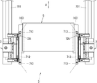
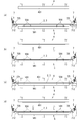
- FIG. 1 is a front view of main components of the printed circuit board inspection apparatus according to the first embodiment of the present invention.
- FIG. 2 is a plan view of the printed circuit board inspection apparatus according to the first embodiment, as viewed from the line XX in FIG.
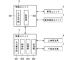
- FIG. 3 is a block diagram of an electrical system configuration of the printed circuit board inspection apparatus according to the first embodiment.
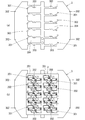
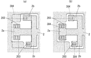
- FIG. 4 is a plan view showing an example of a tray and a printed circuit board placed on the tray.
- FIG. 5 is a diagram showing a state in which a part of the printed circuit board 2 placed on the tray is looked up from below.
- FIG. 6 is a cross-sectional view of a main part of the upper inspection jig according to the first embodiment.
- FIG. 7 is a front view of the substrate transfer unit according to the first embodiment.
- FIG. 8 is a plan view of the substrate transfer unit.
- FIG. 9 is a side view of the substrate transport unit.
- FIG. 10 is a flowchart for explaining the operation of the printed circuit board inspection apparatus.
- FIG. 11 is a main part front view for explaining the operation of the upper inspection jig and the lower inspection jig.
- FIG. 12 is a plan view illustrating the configuration of the substrate reversing unit and the punching unit of the printed circuit board inspection apparatus according to the second embodiment.
- FIG. 1 is a diagram of main components of a printed circuit board inspection apparatus (hereinafter simply referred to as “inspection apparatus”) according to a first embodiment of the present invention
- FIG. 2 is a cross-sectional view taken along line XX in FIG.
- FIG. 3 is a block diagram showing the configuration of the electrical system of the inspection apparatus.
- the support column 601 is omitted, and only the outline of the tray 3 is indicated by a two-dot chain line in consideration of easy viewing.
- the inspection apparatus 1 is mainly used for inspection of a flexible printed circuit board (hereinafter simply referred to as “printed circuit board”) in which wiring is formed on both front and back surfaces, and performs inspection of wiring on the upper surface of the printed circuit board 2.
- the first characteristic point of the inspection apparatus is that the inspection is performed in a state where the above-described flexible printed circuit board 2 is placed on the flat tray 3.
- the printed circuit board is vacuum-adsorbed and fixed to the plate so that inspection defects due to warping or twisting of the printed circuit board do not occur. Or inspected with the edge of the substrate pulled by a clamper.
- inspection is performed in a state where the printed circuit board 2 placed on the flat tray 3 is sandwiched between the upper inspection jig 4 and the lower inspection jig 5. If the inspection of the flexible printed circuit board 2 is performed in a state where it is placed on the tray 3, no warping or twisting occurs on the printed circuit board, so there is no need to suck the printed circuit board or pull it with a clamper. Furthermore, since a simple configuration in which the printed circuit board 2 placed on the tray 3 is sandwiched between the upper inspection jig 4 and the lower inspection jig 5 can be employed, the cost of the inspection apparatus can be significantly reduced.
- FIG. 4 (a) shows an example of the tray 3
- FIG. 4 (b) shows an example of the printed circuit board 2 placed on the tray 3.
- the flat tray 3 made of an insulating synthetic resin is formed with four guide pins 301, a plurality of positioning holes 302 and 303, and a plurality of openings 304.
- wiring 201 and a plurality of positioning holes 202 are formed in the printed circuit board 2.
- the guide pins 301 also serve to prevent the printed circuit board 2 from falling off. By inserting the guide pins 301 into the four holes 202 provided at opposite positions of the printed circuit board 2, the printed circuit board 2 is firmly attached to the tray 3. Fixed. Therefore, when the tray 3 is transported using the substrate transport unit 7, the printed circuit board 2 is not dropped from the tray 3 or shifted in position.
- the four holes 302 formed at the left and right ends of the tray 3 are used when the tray 3 is transported using the substrate transport unit 7, and guide pins 713 ( If the tray 3 is transported in a state in which it is inserted, the tray 3 will not fall out of the substrate transport unit 7.
- the other holes 303 formed in the tray 3 and the holes 202 formed at positions facing the printed circuit board 2 are positioning holes for the inspection jig, and are provided in the lower inspection jig 5 in these holes. By inserting the guide pins 504, the printed circuit board 2 is accurately positioned with respect to the lower inspection jig 5.
- the plurality of openings 304 provided in the tray 3 are used for bringing the inspection pins of the lower inspection jig 5 into contact with the inspection target portions (for example, pads) of the wiring 201 formed on the lower surface of the printed board 2 at the time of inspection. Is.
- the inspection can be performed without any trouble even when the printed circuit board 2 is placed on the tray 3.
- the upper inspection jig 4 is lowered using the lifting unit 6, and the printed circuit board 2 placed on the flat tray 3 is sandwiched between the upper inspection jig 4 and the lower inspection jig 5.
- the inspection pins provided on each inspection jig are brought into contact with the pads of the printed circuit board 2 to inspect for wiring continuity and insulation defects.
- FIG. 5 shows a state in which a part of the printed circuit board 2 placed on the tray 3 is looked up from below.
- the satin-like portion indicates the printed circuit board 2
- the two-dot chain line indicates the opening 304.
- 5A and FIG. 5B the size and number of the opening portions 304 formed in the tray 3 are different.
- the size of the opening 304 is kept to the minimum necessary, and in particular, in the place where the slit is formed in the printed circuit board 2, consideration is given to the position and size of the opening so that the printed circuit board 2 is not warped or twisted. There is a need to.
- the printed circuit board 2 shown in FIGS. 5A and 5B includes three branch portions 2a, 2b, and 2c, and slits are formed around the branch portions. Further, a pad 203 which is a part of the wiring 201 is formed at each branch portion. In the inspection, the printed circuit board 2 is sandwiched between the upper inspection jig 4 and the lower inspection jig 5, and the inspection pins of the lower inspection jig 5 are in contact with the pads 203 through the openings 304. Apply voltage to
- the ends of the branches 2a, 2b, and 2c are self-weighted. May cause warping or twisting, and the inspection pin may not contact the target pad 203 in some cases.
- FIG. 5B if openings 304 having a relatively small area are formed at positions facing the pads of the three branches 2a, 2b and 2c, the branches 2a, 2b and 2c are hardly bent, and the risk that the inspection pin does not contact the pad 203 due to warping or twisting can be avoided.
- the printed circuit board 2 is inspected while being sandwiched between the upper inspection jig 4 and the lower inspection jig 5 and accurately positioned by the guide pins 504 and the positioning holes 202. High inspection is possible. The inspection process will be described in detail later with reference to FIGS.
- the positions and sizes of the guide pins 301, the holes 302 and 303, and the openings 304 of the tray 3 vary depending on the shape of the wiring pattern formed on the printed circuit board 2 and the repeated pitch. Therefore, it is necessary to prepare a tray having a shape corresponding to the target printed circuit board.
- the second feature of the inspection apparatus is that the inspection of the printed circuit board 2 on which a plurality of wiring patterns having the same shape are formed is performed a plurality of times by dividing the target area. As described above, when a printed circuit board is manufactured, a plurality of wiring patterns having the same shape are formed on a single sheet-like printed circuit board 2 having a large area, and after the inspection is completed, they are cut into individual patterns. Separated into printed circuit boards. The inspection apparatus of the present invention inspects the sheet-like printed circuit board 2 before being cut.
- a total of 10 wiring patterns are regularly arranged on the printed circuit board 2 in five rows each having a pair of wiring patterns of the same shape. If these ten wiring patterns are to be inspected simultaneously, a huge number of inspection pins are required for the inspection jig, which makes the inspection jig expensive. In addition, the proportion of poor contact with the substrate increases. In order to avoid this, in the inspection apparatus of the present invention, inspection is performed using an inspection jig provided with a number of inspection pins corresponding to a pair of left and right wiring patterns.
- the tray 3 is transported in the horizontal direction (direction indicated by arrow A in FIG. 2) by the pair of substrate transport units 7 and 7 disposed on the left and right of the lower inspection jig 5. Is done.
- the substrate transport unit 7 has a function of transporting the tray 3 placed on the tray base 712 in the horizontal direction with the end of the tray 3 sandwiched between the chucks 725, and a function of placing the tray 3 on the lower inspection jig 5. It has.
- the substrate transport unit 7 will be described in detail later with reference to the drawings.
- the inspection apparatus according to the present invention is optimal as an inspection apparatus for a flexible printed board having wirings formed on both sides, but is not limited to the inspection of a flexible printed board having wirings formed on both sides. . Even in the inspection of a flexible printed circuit board or a hard printed circuit board in which wiring is formed only on one surface, the inspection of the printed circuit board can be performed automatically and in a short time by taking advantage of the two feature points described above.
- the inspection apparatus according to the present invention is used for inspection of a flexible printed circuit board in which wiring is formed only on one surface, the same shape and structure as the lower inspection jig 5 instead of the lower inspection jig 5 A dummy jig having an inspection pin but no inspection pin is prepared, and a tray is placed thereon for inspection.
- the inspection apparatus 1 applies a voltage between the control unit 8 that controls the operation of the elevating unit 6 and the substrate transport unit 7 and the inspection pins of the upper inspection jig 4 and the lower inspection jig 5, and the resistance therebetween. And an inspection unit 9 for measuring values.
- the control unit 8 and the inspection unit 9 are accommodated in a casing of an inspection apparatus that is separately installed.
- the control unit 8 is composed of a programmable logic controller, and controls the operations of the elevating unit 6 and the substrate transport unit 7 based on data input from the input display unit 801 and stored in the storage unit 802.
- the lifting unit 6 moves the upper inspection jig 4 in the vertical direction by driving the air cylinder.
- the board transport unit 7 drives the motor and the air cylinder to transport the tray 3 on which the printed circuit board 2 is placed in the horizontal direction or move it in the vertical direction.
- the input display unit 801 of the control unit 8 is composed of a touch panel type liquid crystal device, and inputs data necessary for operating the elevating unit 6 and the substrate transport unit 7 and displays the data.
- the storage unit 802 includes a flash memory or the like and stores data input from the input display unit 801.
- the inspection unit 9 is composed of a personal computer, and includes an input display unit 901, a measurement unit 902, a storage unit 903, and a control unit 904.
- the function of the control unit 904 is realized by executing a program read from the storage unit 903 by a CPU (Central processing Unit, not shown).
- the input display unit 901 of the inspection unit 9 is composed of a touch panel type liquid crystal device, and is used for inputting data necessary for determining the quality of continuity and insulation, and for displaying the result of determination of quality of continuity and insulation.
- the measuring unit 902 applies a voltage between the two inspection pins selected from the inspection pins of the upper inspection jig 4 and the lower inspection jig 5 via the wiring 201 of the printed circuit board 2, and between them Measure the resistance value.
- the storage unit 903 is usually composed of an HDD (Hard Disk Drive), and is used to store programs and data input from the input display unit 901, data of determination results, and the like.
- HDD Hard Disk Drive
- the control unit 904 compares the resistance value measured by the measurement unit 902 with the resistance value of a good printed circuit board stored in the storage unit 903, and determines whether the target printed circuit board is conductive or insulated. The determination result is stored in the storage unit 903 and displayed on the input display unit 901 as necessary.
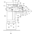
- the lifting unit 6 and the upper inspection jig 4 will be described.
- the lifting / lowering unit 6 moves the upper inspection jig 4 in the vertical direction.
- the lifting unit 6 includes a top plate 602 supported by four columns 601 installed on the base 101, a plate 603 that supports the upper inspection jig 4, and a cylinder body attached to the top plate 602.
- An air cylinder 604 whose tip is fixed to the plate 603 via a joint, and a linear guide 606 that is attached to four corners of the plate 603 and guides the vertical movement of the plate 603 together with the column 601.
- the upper inspection jig 4 is attached to the plate 603. Specifically, a pair of left and right long fixtures 607 and 607 are installed on the lower surface of the plate 603, and the left and right ends of the support plate 402 of the upper inspection jig 4 are inserted into the grooves of the fixture 607. By doing so, the upper inspection jig 4 is attached to the plate 603.
- the upper inspection jig 4 includes an inspection board 401 having a plurality of inspection pins, a support plate 402 made of a flat plate-shaped synthetic resin for attaching the upper inspection jig 4 to the plate 603 of the elevating unit 6, and an inspection board It is composed of a plurality of columns 403 for fixing 401 to the support plate 402.
- the space between the inspection board 401 and the support plate 402 is a passage for a lead wire drawn out from the inspection pin of the inspection board 401.
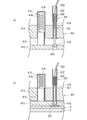
- FIG. 6 is a cross-sectional view of the main part of the inspection board 401.
- FIG. 6A shows a state before inspection
- FIG. 6B shows a state during inspection.
- the inspection board 401 is a laminate of two boards 411 and 412 made of an insulating resin. A push member 413 and a probe 417 are attached to the main board 411, and a guide hole 424 for guiding the inspection pin is formed in the guide board 412.
- the pushing member 413 presses the guide board 412 in a direction away from the main board 411.
- the pushing member 413 includes a bottomed cylindrical case 414 fixed to the main board 411, a columnar pushing pin 415 inserted into the case 414, and a compression spring 416 inserted between the case 414 and the pushing pin 415. It consists of The guide board 412 is separated from the main board 411 by the repulsive force of the compression spring 416 when not inspected.
- the probe 417 abuts the inspection pin 418 on the inspection target portion (for example, the pad 203 shown in FIG. 5) during the inspection.
- the probe 417 is fixed to the inspection pin 418 and the main board 411.
- a bottomed cylindrical socket 419, a compression spring 420 inserted between the socket 419 and the rear end 421 of the inspection pin 418, and an insulating pipe 422 for preventing electric shock attached to the rear end of the socket 419 It consists of
- the inspection pin 418, the compression spring 420, and the socket 419 are made of conductive metal, and a lead wire 423 is connected to the rear end of the socket 419. As shown in FIG. 6A, the inspection pin 418 is always biased toward the guide board 412 by the compression spring 420.
- the pushing member 413 and the probe 417 are attached to the main board 411 one by one. However, in the actual inspection board 401, the pushing member 413 is arranged so that the force pushing the guide board 412 is equalized. These are attached to the four corners of the rectangular parallelepiped main board 411, respectively. Probes 417 are attached to positions on the printed circuit board 2 that are opposed to the inspection target portions.
- the inspection pin 418, the socket 419 and the compression spring 420 are made of a conductive material, when a constant voltage is applied between the two inspection pins 418 selected by the inspection unit 9. A current flows between the inspection pins via the wiring 201.
- the resistance value between the inspection pins is measured by a measuring instrument built in the measuring unit 902 and the value is compared with the value of a non-defective printed circuit board stored in the storage unit 903 in the control unit 904, The quality of continuity and insulation can be determined.
- the structure of the inspection board 401 shown in FIG. 6 is an example, and is not limited to this structure.
- An inspection board having another structure may be adopted as long as the same function can be exhibited.
- the lower inspection jig 5 inspects the wiring formed on the lower surface of the printed circuit board 2.
- the inspection board 501 having a plurality of inspection pins and the lower inspection jig 5 are fixed to the base 101.
- the lower inspection jig 5 is attached to a plate 102 fixed to the base 101.
- a pair of long fixtures 103 are provided on the left and right sides of the plate 102. By inserting the left and right ends of the support plate 502 of the lower inspection jig 5 into the grooves of the fixture 103, The inspection jig 5 is attached to the plate 102.
- the difference between the upper inspection jig 4 and the lower inspection jig 5 described above is that the upper inspection jig 4 can be moved in the vertical direction by the lifting unit 6, whereas the lower inspection jig 5 is based on the plate 102.
- a guide pin 504 for positioning the printed circuit board 2 is attached to the point fixed to the base 101 and the inspection board 501, and a hole (not shown) for accommodating the guide pin 504 is provided at a position facing the upper inspection jig 4. ) Is formed.
- the printed circuit board 2 becomes a lower inspection jig. 5 is accurately positioned, and the inspection pin comes into contact with the wiring (for example, pad) 201 of the inspection object portion without error.
- the lift unit 6 is driven to lower the plate 603, and the printed circuit board 2 placed on the tray 3 is sandwiched between the upper inspection jig 4 and the lower inspection jig 5. After the inspection is completed, the lift unit 6 is driven to raise the plate 603 and then held at the position shown in FIG.
- FIGS. 7 is a front view of the left unit of the pair of substrate transfer units 7 and 7 in FIG. 1, FIG. 8 is a plan view of the unit, and FIG. 9 is a side view of the unit.
- tubes, valves, motors and various sensors for supplying compressed air to the air cylinder and wiring for connecting the control unit 8 are omitted.
- bolts and nuts for fixing the members are shown in the figure, these are general-purpose fastening members and will not be described with reference numerals.
- the substrate transport unit 7 transports the tray 3 on which the printed circuit board 2 is placed in the horizontal direction.
- a pair of slide tables 701 having a rectangular cross section are installed on the left and right sides of the lower inspection jig 5 along the movement path.
- the slide table 701 is a member for transporting the tray 3 in the horizontal direction.
- a ball screw (not shown) accommodated in the table is rotated, the slide block 702 is indicated by an arrow A on the slide table 701. Move in the direction.
- a guide mounting plate 704 and a first air cylinder 705 are mounted on the upper surface of the support plate 703 by bolts or the like.
- One end of the first connecting plate 707 is attached to the upper portion of the piston rod 706 of the air cylinder 705 via a joint, and the other end of the first connecting plate 707 is sandwiched between the guide attaching plate 704.
- An arm base 711 having an L-shaped cross section is attached.
- 1st linear guide 708 which guides the raising / lowering of the arm base 711 is attached to the side surface of the guide attachment plate 704.
- the first linear guide 708 includes a rail 709 attached to the guide attachment plate 704 and a block 710 attached to the arm base 711.
- the connecting plate 707 is moved up and down by contracting or extending the piston rod 706 of the first air cylinder 705
- the block 710 moves up and down along the rail 709, thereby enabling the arm base 711 to move up and down smoothly. Yes.
- a tray base 712 having guide pins 713 installed at both ends is attached to the top surface of the tip of the arm base 711. As shown in FIG. 1, the end of the tray 3 is placed on the tray base 712. The tray 3 is transported. At this time, the guide pins 713 are inserted into the positioning holes 302 (see FIG. 3) formed at the end of the tray 3.
- a second air cylinder 715 is attached to the lower surface of the first connecting plate 707, and a second connecting plate 717 having an L-shaped cross section is attached to the tip of the piston rod 716 via a joint. ing. Further, a pair of cylinder mounting plates 718 and 718 having a U-shaped cross section are attached to both ends of the second connecting plate 717 via bolts, respectively.
- a third air cylinder 721 is accommodated in the groove of the cylinder mounting plate 718.
- the rear portion of the air cylinder 721 is rotatably attached to the cylinder attachment plate 718 via a pin 722, and the front end of the piston rod 723 is connected to the chuck 725 via a hinge pin 724.
- the chuck 725 sandwiches the end of the tray 3 placed on the tray base 712, and is attached to the cylinder mounting plate 718 in a rotatable state via a pin 726 disposed at the lower part.
- the piston rod 723 is contracted, the chuck 725 rotates counterclockwise around the pin 726 as shown by a two-dot chain line in FIG. 7, and the tray 3 is released from gripping by the chuck 725.
- a urethane sheet 727 is affixed to the lower surface of the chuck 725 to prevent rattling that occurs when the tray 3 is sandwiched between the chuck 725 and the tray base 712.
- a second linear guide 731 is installed between the cylinder mounting plate 718 and the arm base 711. As shown in FIG. 9, the second linear guide 731 includes a rail 732 attached to the upper surface of the arm base 711 in parallel with the cylinder attachment plate 718 and a block 733 attached to the lower surface of the cylinder attachment plate 718. Then, the movement of the cylinder mounting plate 718 in the horizontal direction (the direction indicated by the arrow C in FIGS. 7 and 8) is guided.
- the reason why the cylinder mounting plate 718 can be moved in the horizontal direction is to prevent the chuck 725 from getting in the way when the operator attaches the tray 3 to the tray base 712 or removes the tray 3 from the tray base 712. It is. As the cylinder mounting plate 718 moves backward, the chuck 725 is retracted to a position where the tray 3 does not contact.
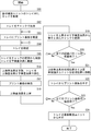
- FIG. 10 is a flowchart showing the flow of the operation of the inspection apparatus 1
- FIG. 11 is a side view of the main part for explaining the operations of the upper inspection jig 4 and the lower inspection jig 5.
- the substrate transfer unit 7 stands by at the position shown in FIG.
- the tray table 712 is held at a position higher than the lower inspection jig 5.
- the chuck 725 is in an open state, and the chuck 725 is further retracted by the linear guide 731, so that it does not get in the way when the operator places the tray 3 on the tray base 712.
- the operator attaches both end portions of the tray 3 to the tray bases 712 of the pair of substrate transport units 7 (step S11).
- the operator inserts the four guide pins 713 attached to the tray base 712 into the four positioning holes 302 (see FIG. 4) formed at both ends of the tray 3, respectively. It mounts on the stand 712 (refer FIG. 2).
- the operator places the printed circuit board 2 on the tray 3, and sets the guide pins 301 of the tray 3 so that the printed circuit board 2 does not fall out of the tray 3.
- the second hole 202 is inserted (step S13). Thus, preparation for transporting the tray 3 is completed.
- step S14 The subsequent operations are automatically performed based on the data stored in the storage unit 802 (see FIG. 3) of the control unit 8.
- the slide table 701 is driven to move the slide block 702 in the horizontal direction, and the wiring pattern for the first inspection on the tray 3 is placed above the lower inspection jig 5. Transport until it comes (step S14)
- Step S15 When the slide block 702 moves to the designated position and stops, the first air cylinder 705 of the tray transport unit 7 is driven, the piston rod 706 is contracted, and the arm base 711 is lowered. As the arm base 711 is lowered, the piston rod 723 of the third air cylinder 721 contracts and the chuck 725 rotates around the pin 726 (see FIG. 7), and the tray 3 is released from the grip of the chuck 725. (Step S15).
- step S16 by driving the air cylinder 604 of the elevating unit 6 and extending the piston rod 605, the upper inspection jig 4 is lowered, and as shown in FIG. 11 (c), the inspection board 401 of the upper inspection jig 4 and The tray 3 is stopped while the tray 3 is sandwiched between the inspection boards 501 of the lower inspection jig 5 (step S16).
- the compression spring 416 of the upper inspection jig 4 is pressed by pressure.
- the tip of the inspection pin 418 is exposed from the guide hole 424 and contacts the wiring 201 formed on the upper surface of the printed board 2.
- the wiring 201 formed on the lower surface of the printed circuit board 2 is also formed on the lower surface of the printed circuit board 2 in the same manner as the upper inspection jig 4 because the compression spring contracts and the tip of the inspection pin is exposed from the guide hole. 201 is contacted.
- the continuity or insulation of the printed circuit board 2 is inspected (step S17). Specifically, the measurement unit 902 of the inspection unit 9 applies a voltage between the two selected inspection pins 418, measures the resistance value between the inspection pins, and sends the value to the control unit 904. .
- the control unit 904 compares the measured resistance value between the inspection pins with the resistance value of a non-defective printed circuit board stored in the storage unit 903, and determines whether the printed circuit board to be inspected is conductive or insulated. Pass / fail judgment is performed. The determination result is displayed on the input display unit 901 by the control unit 904 and further written in the storage unit 903.
- the air cylinder 604 of the elevating unit 6 is driven to contract the piston rod 605, whereby the upper inspection jig 4 is raised to the position shown in FIG. S18).
- the position of the upper inspection jig 4 shown in FIG. 11 (d) is set lower than the position of the upper inspection jig 4 shown in FIG. 11 (b). This is for shortening the descent time of the upper inspection jig 4 when performing the next inspection.
- the first air cylinder 705 of the substrate transport unit 7 is driven, the piston rod 706 is extended, the arm base 711 is raised, and the tray 3 is separated from the lower inspection jig 5.
- the third air cylinder 721 of the substrate transport unit 7 operates slightly later than the start of raising the tray 3, the piston rod 723 extends, the chuck 725 rotates clockwise around the pin 726, and between the tray table 712. Then, the end of the tray 3 is gripped again (step S19).
- the tray 3 When the tray 3 is raised, the printed circuit board 2 fixed to the lower inspection jig 5 by the guide pins 504 is detached from the lower inspection jig 5 with the guide pins 504 removed from the positioning holes 202. Finally, the tray 3 is raised to the position shown in FIG.
- the control unit 904 of the inspection unit 9 confirms from the inspection data stored in the storage unit 903 whether or not the inspection of all the wiring patterns on the printed circuit board 2 has been completed (step S20). (No in the same step), the process returns to step S14, and the processes of steps S14 to S19 are repeated.
- control unit 904 determines that the inspection of all the wiring patterns of the printed circuit board 2 has been completed (Yes in step S20)
- the control unit 904 transmits data indicating that the inspection has been completed to the control unit 8.
- the control unit 8 raises the upper inspection jig 4 to the initial position shown in FIG. 11A, and drives the slide table 701 to move the substrate transport unit 7 to the initial position (step S21).
- the operator removes the printed circuit board 2 placed on the tray 3 from the tray 3 (step S22).
- the operator determines that conduction or insulation is poor among the printed circuit boards 2 removed from the tray 3 based on the inspection result displayed on the input display unit 901 of the inspection unit 9.
- a sticker on which an identification mark is displayed is pasted at the place of the printed wiring pattern.
- the printed circuit board 2 on which the identification seal is affixed is separated for each wiring pattern by a cutter (not shown). Of the individually separated printed boards, the board with the identification sticker is discarded, and only good printed boards are shipped as products.
- step S23 the operator determines whether or not the inspection of all the printed circuit boards to be inspected has been completed. If there is no printed circuit board (No), the process returns to step S13 to place a new printed circuit board 2 on the tray 3.
- Step S23 when the inspection has been completed for all the printed boards (Yes in Step S23), the process proceeds to Step S24, and the operator removes the tray 3 from the board transport unit 7. Specifically, when the operator presses the button of the control unit 8, the piston rod 723 of the third air cylinder 721 of the substrate transport unit 7 is contracted, the chuck 725 is rotated around the pin 726, and the tray 3 is chucked. Release from gripping by 725. Further, the piston rod 716 of the second air cylinder 715 contracts and the chuck 725 moves backward.
- the operator removes the tray 3 from the tray base 712. At this time, since the chuck 7 is in the retracted position, it does not get in the way when the tray 3 is removed from the tray base 712.
- the inspection apparatus when the inspection apparatus according to the present embodiment is used, it is not necessary to consider warping or twisting of the flexible printed circuit board, so that the configuration of the apparatus is simplified, and as a result, the inspection apparatus can be manufactured at low cost. . Moreover, since the wiring on both sides of the printed circuit board can be inspected simultaneously, the time required for the inspection can be shortened.
- air cylinders are used as driving means for the elevating unit 6 and the substrate transport unit 7, but the present invention is not limited to this. It goes without saying that the same function can be realized even if a hydraulic cylinder or an actuator driven by an electromagnet is used as the driving means.
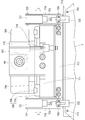
- FIG. 12 shows the substrate reversing unit 11 and the punching unit 12 disposed in the vicinity of the rear portion of the slide table 701.
- ⁇ Substrate reversing unit> As shown in FIG. 4B described above, a plurality of the same wiring patterns are regularly formed on the printed circuit board 2. After the inspection of the printed circuit board 2 is completed, the printed circuit board 2 is cut and separated into individual printed circuit boards.
- the wiring pattern shown in FIG. 4B will be further described.
- one wiring pattern and a wiring pattern obtained by inverting the wiring pattern are arranged close to each other. It is a thing.
- the wiring pattern direction may be reversed for each pitch.
- the entire board can be inspected simply by repeatedly carrying the printed board 2 by the board carrying unit 7.
- the upper inspection jig 4 and the lower inspection jig 5 having the number of inspection pins 418 corresponding to the pair of wiring patterns are used.
- the printed circuit board 2 By inspecting the printed circuit board 2 as a whole by repeating the inspection while shifting the wiring pattern by one pitch by the substrate transport unit 7.
- the printed circuit board is rotated by 180 degrees using the substrate reversing unit 11, and then the wiring pattern in the reverse direction is used.
- the wiring is inspected in the same manner as in the forward direction. In this way, it is not necessary to prepare an inspection jig having two types of inspection pins, so that inspection costs can be reduced.
- the configuration and operation of the substrate reversing unit 11 will be described with reference to FIG.
- the substrate reversing unit 11 is controlled by the control unit 8 described in the first embodiment.
- the substrate reversing unit 11 includes a table 111 on which the tray 3 transported by the substrate transport unit 7 is placed, an air cylinder 112 that rotates the table 111, and an air cylinder 113 that moves the table 111 up and down.
- FIG. 12 shows the outline of the tray 3 placed on the table 111 with a two-dot chain line.
- Guide pins 114 are provided at the four corners of the table 111, respectively. By inserting the guide pins 114 into the holes formed at the opposite positions of the tray 3, the tray 3 is positioned with respect to the table 111 and further prevents the tray 3 from dropping from the table 111.
- the rotating shaft of the air cylinder 112 which is a driving means is connected to the lower surface of the center of the table 111. Since the rotation shaft is installed at the intermediate point between the pair of slide tables 701 and 701, when the tray 3 placed on the table 111 is rotated 180 degrees by the air cylinder 113, the tray 3 is the same with respect to the slide table 701. Held in position.
- the operation of the substrate reversing unit 11 will be described.
- the piston rod (not shown) of the air cylinder 113 is contracted so as not to hinder the transport of the tray 3 by the substrate transport unit 7, so positioned.
- the printed circuit board 2 for which the inspection of the wiring pattern in the forward direction has been completed is transported to the position indicated by the two-dot chain line in FIG. Thereafter, the tray 3 is released from the grip of the chuck 725, and the chuck 725 is further retracted to a position where it does not interfere with the removal of the tray 3 by the linear guide 731.
- the tray 3 stops above the tray base 712, and the air cylinder 112 rotates at that position to rotate the tray 3 180 degrees.
- the piston rod (not shown) of the air cylinder 113 is contracted to lower the table 111, and the inverted tray 3 is placed on the tray base 712.
- the table 111 is lowered to the bottom of the tray table 712 and then stops.
- the chuck 725 moves forward by the linear guide 731 and further grips the end of the tray 3 placed on the tray base 712.
- the inverted tray 3 is transported to a position where the inspection by the inspection jigs 4 and 5 is performed, and the wiring pattern in the reverse direction is inspected according to the above-described procedure.
- ⁇ Punching unit> As described with reference to the flowchart of FIG. 10, the printed circuit board 2 that has been inspected is separated for each wiring pattern, and only a board that is determined to be non-defective is shipped. If an identification mark is given to a wiring pattern determined to have poor conduction or insulation failure at the time of separation, only the substrate needs to be discarded after the division, so that the time required for separation can be shortened.
- the seal is pasted as an identification mark on the wiring pattern that is determined to be defective by the operator.
- manual operation by the operator is necessary, which causes an increase in cost.
- the time required for the inspection becomes longer.
- identification mark applying means for applying an identification mark to a wiring pattern determined to be defective among the wiring patterns of the printed circuit board. Specifically, a hole is made as an identification mark in the wiring pattern determined to be defective using the punching unit 12 so that the wiring pattern determined to be poor conduction or insulation failure can be seen at a glance.
- the punching unit 12 includes an upper puncher 121, a lower puncher 122, an air cylinder 123 that moves the lower puncher 122 up and down, and a slider 124 that moves the air cylinder 123 in the horizontal direction.
- the punching unit 12 is controlled by the control unit 8 in the same manner as the substrate reversing unit 11.
- the upper puncher 121 and the lower puncher 122 are attached to the upper end portion and the lower end portion of the U-shaped arm, and are configured to be moved integrally in the horizontal direction by the slider 124.
- the upper puncher 121 is also provided with an air cylinder for moving the puncher up and down. However, since this performs the same function as the air cylinder 123, it is omitted in FIG. is doing.
- the upper puncher 121 When the upper puncher 121 is not in operation, the upper puncher 121 is held at a position higher than the tray base 712 so as not to prevent the substrate transport unit 7 from transporting the tray 3 by driving an air cylinder (not shown). Similarly, the lower puncher 122 is held at a position lower than the tray base 712 by driving the air cylinder 123.
- the tray 3 is transported to the rear part of the slide table 701 by the substrate transport unit 7.
- the substrate transport unit 7 stops. Thereafter, by driving the slider 124, the upper puncher 121 and the lower puncher 122 stop at a position where the opening 304 of the tray 3 is located.
- the printed circuit board 2 in which the hole is formed in the wiring pattern having poor conduction or insulation failure is transported to the initial position by the board transport unit 7 and then removed from the tray 3 by the operator's hand.
- the printed circuit board 2 removed from the tray 3 is separated for each wiring pattern. However, since the wiring pattern with poor conduction and insulation is perforated, the quality of the printed circuit board can be easily identified.
- the printed board is perforated as a mark for identifying a wiring pattern having poor conduction or insulation, but the identification mark is not limited to this.
- a sticker may be attached to a corresponding portion of the printed board.
- an air cylinder is used as a driving means for the substrate reversing unit 11 and the punching unit 12 as in the case of the lifting unit 6 and the substrate transport unit 7, but an actuator using a hydraulic cylinder or an electromagnet instead of these. It goes without saying that may be used.
- the table 111 of the substrate reversing unit 11 and the slider 124 of the punching unit 12 are installed in a partially overlapping state, but this is intended for effective use of space. If there is no hindrance to raising and lowering the table 111 and the lower puncher 122, there is no particular problem even if they are installed at overlapping positions.
Landscapes
- Engineering & Computer Science (AREA)
- Microelectronics & Electronic Packaging (AREA)
- Physics & Mathematics (AREA)
- General Physics & Mathematics (AREA)
- Computer Hardware Design (AREA)
- General Engineering & Computer Science (AREA)
- Testing Of Short-Circuits, Discontinuities, Leakage, Or Incorrect Line Connections (AREA)
- Environmental & Geological Engineering (AREA)
Abstract
Description
前記プリント基板を載置する、絶縁材料で形成された板状のトレイと、
前記プリント基板の上面の配線の検査を行う上検査治具および下面の配線の検査を行う下検査治具と、
前記下検査治具の上方に配置された前記上検査治具を下降させ、かつ前記トレイに載置された状態のプリント基板を前記上検査治具および下検査治具で挟むことにより、前記上検査治具の検査ピンと前記プリント基板の配線とを接触させる昇降ユニットと、
前記上検査治具の選択された2本の検査ピンの間に電圧を印加すると共に、それらの間の抵抗値を計測する検査ユニットと、
前記昇降ユニットの動作を制御する制御ユニットと、を備えたことを特徴とする。 In order to achieve the above object, a printed circuit board inspection apparatus according to the present invention brings an inspection pin into contact with a predetermined portion of a wiring of a printed circuit board having wiring formed on at least one surface, and two selected A printed circuit board inspection apparatus that inspects the continuity or insulation of the printed circuit board by applying a voltage between the inspection pins through the wiring,
A plate-like tray formed of an insulating material on which the printed circuit board is placed;
An upper inspection jig for inspecting wiring on the upper surface of the printed circuit board and a lower inspection jig for inspecting wiring on the lower surface;
The upper inspection jig placed above the lower inspection jig is lowered, and the printed circuit board placed on the tray is sandwiched between the upper inspection jig and the lower inspection jig, thereby An elevating unit for contacting the inspection pin of the inspection jig and the wiring of the printed circuit board;
An inspection unit that applies a voltage between two selected inspection pins of the upper inspection jig and measures a resistance value between them;
And a control unit for controlling the operation of the lifting unit.
<プリント基板検査装置の構成>
図1は、本発明の実施の形態1にかかるプリント基板検査装置(以降、単に「検査装置」という)の主要構成部材を正面から見た図、図2は、図1のX-X線から下方を見た図、図3は、検査装置の電気系の構成を示すブロック図である。なお、図2では支柱601を省略し、また見易さを考慮して、トレイ3については輪郭のみを2点鎖線で示している。 (Embodiment 1)
<Configuration of printed circuit board inspection device>
FIG. 1 is a diagram of main components of a printed circuit board inspection apparatus (hereinafter simply referred to as “inspection apparatus”) according to a first embodiment of the present invention, and FIG. 2 is a cross-sectional view taken along line XX in FIG. FIG. 3 is a block diagram showing the configuration of the electrical system of the inspection apparatus. In FIG. 2, the
次に、図10および図11、更には前述の各図面を参照して、本発明にかかる検査装置1の動作を説明する。図10は、検査装置1の動作の流れを示すフローチャート、図11は、上検査治具4と下検査治具5の動作を説明する要部側面図である。 <Operation of board inspection device>
Next, the operation of the
本実施の形態は、実施の形態1の検査装置1のスライドテーブル701の後部の近傍に基板反転ユニット11とパンチングユニット12を設置したものである。図12に、スライドテーブル701の後部近傍に配された基板反転ユニット11とパンチングユニット12を示す。以下、それぞれのユニットを設ける理由と構成について説明する。 (Embodiment 2)
In the present embodiment, a
前述の図4(b)に示すように、プリント基板2には同一の配線パターンが複数個規則正しく形成されている。プリント基板2の検査が終了した後、プリント基板2を切断して個別のプリント基板に分離する。 <Substrate reversing unit>
As shown in FIG. 4B described above, a plurality of the same wiring patterns are regularly formed on the printed
図10のフローチャートを用いて説明したように、検査を終えたプリント基板2は、個々の配線パターン毎に分離され、良品と判定された基板のみ出荷される。分離の際、導通不良または絶縁不良と判定された配線パターンに識別マークが付与されていれば、分割後、その基板だけを廃棄すればよいため、分別にかかる時間を短縮できる。 <Punching unit>
As described with reference to the flowchart of FIG. 10, the printed
2 プリント基板
3 トレイ
4 上検査治具
5 下検査治具
6 昇降ユニット
7 基板搬送ユニット
8 制御ユニット
9 検査ユニット
11 基板反転ユニット
12 パンチングユニット
101 基台
102、603 プレート
103、607 取付具
111 テーブル
112 回転軸
113、123、604、705、715、721 エアシリンダ
121 上パンチャー
122 下パンチャー
124 スライダー
201 配線
202、302、303 位置決め用孔
203 パッド
301、504、713 ガイドピン
304 開口部
401、501 検査ボード
402、502 支持板
403、503、601 支柱
411、412 ボード
413 押出部材
414 ケース
415 押出ピン
416、420 圧縮バネ
417 プローブ
418 検査ピン
419 ソケット
422 絶縁パイプ
423 リードワイヤ
602 天板
605、706、716、723 ピストンロッド
606、708、731 リニアガイド
701 スライドテーブル
702 スライドブロック
704 ガイド取付板
707、717 連結板
711 アームベース
712 トレイ台
718 シリンダ取付板
724、716 ピン
727 ウレタンフォーム
800 プロセッサ
801、901 入力表示部
802、903 記憶部
902 計測部
904 制御部 DESCRIPTION OF
Claims (11)
- 少なくとも一方の面に配線が形成されたプリント基板の当該配線の所定の箇所に検査ピンを接触させると共に、選択された2本の検査ピンの間に、前記配線を介して電圧を印加して前記プリント基板の導通または絶縁の良否を検査するプリント基板検査装置であって、
前記プリント基板を載置する、絶縁材料で形成された板状のトレイと、
前記プリント基板の上面の配線の検査を行う上検査治具および下面の配線の検査を行う下検査治具と、
前記下検査治具の上方に配置された前記上検査治具を下降させ、かつ前記トレイに載置された状態のプリント基板を前記上検査治具および下検査治具で挟むことにより、前記上検査治具の検査ピンと前記プリント基板の配線とを接触させる昇降ユニットと、
前記上検査治具の選択された2本の検査ピンの間に電圧を印加すると共に、それらの間の抵抗値を計測する検査ユニットと、
前記昇降ユニットの動作を制御する制御ユニットと、を備えたことを特徴とするプリント基板検査装置。 An inspection pin is brought into contact with a predetermined portion of the wiring of the printed circuit board on which wiring is formed on at least one surface, and a voltage is applied between the selected two inspection pins via the wiring. A printed circuit board inspection device that inspects the continuity or insulation of a printed circuit board,
A plate-like tray formed of an insulating material on which the printed circuit board is placed;
An upper inspection jig for inspecting wiring on the upper surface of the printed circuit board and a lower inspection jig for inspecting wiring on the lower surface;
The upper inspection jig placed above the lower inspection jig is lowered, and the printed circuit board placed on the tray is sandwiched between the upper inspection jig and the lower inspection jig, thereby An elevating unit for contacting the inspection pin of the inspection jig and the wiring of the printed circuit board;
An inspection unit that applies a voltage between two selected inspection pins of the upper inspection jig and measures a resistance value between them;
And a control unit for controlling the operation of the elevating unit. - 前記下検査治具の検査ピンは、前記トレイに形成された開口部を通して前記プリント基板の下面の配線に接触し、
前記検査ユニットは、前記上検査治具および下検査治具の選択された2本の検査ピンの間に電圧を印加すると共に、それらの間の抵抗値を計測する、請求項1に記載のプリント基板検査装置。 The inspection pin of the lower inspection jig contacts the wiring on the lower surface of the printed circuit board through the opening formed in the tray,
The print according to claim 1, wherein the inspection unit applies a voltage between two selected inspection pins of the upper inspection jig and the lower inspection jig and measures a resistance value therebetween. Board inspection equipment. - 前記トレイの上面には、前記プリント基板に形成された位置決め用の孔に挿入される第1のガイドピンが取り付けられている、請求項1または2に記載のプリント基板検査装置。 The printed circuit board inspection apparatus according to claim 1 or 2, wherein a first guide pin inserted into a positioning hole formed in the printed circuit board is attached to an upper surface of the tray.
- 前記下検査治具の上面には、前記プリント基板およびトレイのそれぞれに形成された位置決め用の孔に挿入される第2のガイドピンが取り付けられている、請求項1ないし3のいずれかに記載のプリント基板検査装置。 The 2nd guide pin inserted in the hole for positioning formed in each of the said printed circuit board and a tray is attached to the upper surface of the said lower inspection jig. Printed circuit board inspection equipment.
- 前記トレイに載置されたプリント基板を水平方向に搬送する一対の基板搬送ユニットを備え、
当該基板搬送ユニットは、
前記トレイの端部が載置されると共に、当該トレイに形成された位置決め用の孔に挿入される第3のガイドピンが上面に取り付けられたトレイ台と、
当該トレイ台とで前記トレイを把持するチャックと、を備えている、請求項1ないし4のいずれかに記載のプリント基板検査装置。 A pair of substrate transport units that transport the printed circuit boards placed on the tray in the horizontal direction,
The board transfer unit
A tray base on which an end portion of the tray is placed and a third guide pin to be inserted into a positioning hole formed in the tray is attached to the upper surface;
The printed circuit board inspection apparatus according to claim 1, further comprising: a chuck that grips the tray with the tray base. - 前記基板搬送ユニットは、前記トレイ台が上下方向に移動できるように構成されており、
検査が終了した後、前記トレイ台に載置されたトレイを上昇させ、前記下検査治具の第2のガイドピンを、前記プリント基板の位置決め用の孔から外す、請求項4に記載のプリント基板検査装置。 The substrate transport unit is configured such that the tray table can move in the vertical direction,
5. The print according to claim 4, wherein after the inspection is finished, the tray placed on the tray table is raised, and the second guide pin of the lower inspection jig is removed from the positioning hole of the printed circuit board. Board inspection equipment. - 前記基板搬送ユニットは、
前記トレイ台に載置されたトレイを搬送する際には、前記トレイ台を前記下検査治具に接触しない位置まで上昇させ、
検査を行う際には、前記トレイ台を前記トレイが前記下検査治具に載置される位置まで下降させる、請求項5または6に記載のプリント基板検査装置。 The substrate transport unit is
When transporting the tray placed on the tray table, raise the tray table to a position where it does not contact the lower inspection jig,
The printed circuit board inspection apparatus according to claim 5 or 6, wherein when performing inspection, the tray base is lowered to a position where the tray is placed on the lower inspection jig. - 前記基板搬送ユニットは、前記トレイが前記下検査治具に載置されたとき、前記チャックによる前記トレイの把持を開放する、請求項5ないし7のいずれかに記載のプリント基板検査装置。 The printed circuit board inspection apparatus according to any one of claims 5 to 7, wherein the substrate transport unit releases gripping of the tray by the chuck when the tray is placed on the lower inspection jig.
- 前記一対の基板搬送ユニットの移動経路に沿って設置された一対のスライドテーブルの間に、前記トレイに載置されたプリント基板の方向を反転させる基板反転ユニットが設置され、
当該基板反転ユニットは、
前記トレイを載置するテーブルと、
当該テーブルを回転させる回転手段と、
当該テーブルを上下方向に移動させる第1の昇降手段と、で構成されていることを特徴とする、請求項1ないし8のいずれかに記載のプリント基板検査装置。 A substrate reversing unit for reversing the direction of the printed circuit board placed on the tray is installed between a pair of slide tables installed along the movement path of the pair of substrate transport units,
The substrate reversing unit is
A table on which the tray is placed;
Rotating means for rotating the table;
9. The printed circuit board inspection apparatus according to claim 1, further comprising a first lifting / lowering unit that moves the table in a vertical direction. - 前記一対の基板搬送ユニットの移動経路に沿って設置された一対のスライドテーブルの間に、前記プリント基板に形成された複数の配線パターンのうち導通不良または絶縁不良と判定された配線パターンに識別用のマークを付与する識別マーク付与手段が設置されている、請求項1ないし9のいずれかに記載のプリント基板検査装置。 Among the plurality of wiring patterns formed on the printed circuit board between the pair of slide tables installed along the movement path of the pair of substrate transport units, the wiring patterns determined to be defective in conduction or insulation are identified. The printed circuit board inspection apparatus according to claim 1, wherein identification mark applying means for applying the mark is provided.
- 前記識別マーク付与手段はパンチングユニットで構成され、
当該パンチングユニットは、
前記プリント基板を挟むように互いに衝突して当該プリント基板に孔を開ける上パンチャーおよび下パンチャーと、
当該上パンチャーおよび下パンチャーを、前記基板搬送ユニットによる搬送方向と直交する方向に移動させるスライダーと、
当該上パンチャーおよび下パンチャーのそれぞれを、上下方向に移動させる第2および第3の昇降手段と、を備えた、請求項10に記載のプリント基板検査装置。 The identification mark applying means is composed of a punching unit,
The punching unit is
An upper puncher and a lower puncher that collide with each other so as to sandwich the printed circuit board and open a hole in the printed circuit board;
A slider for moving the upper puncher and the lower puncher in a direction perpendicular to the transport direction by the substrate transport unit;
The printed circuit board inspection apparatus according to claim 10, further comprising second and third elevating units that move the upper puncher and the lower puncher in the vertical direction.
Priority Applications (2)
| Application Number | Priority Date | Filing Date | Title |
|---|---|---|---|
| KR1020157036531A KR101735992B1 (en) | 2013-08-12 | 2014-08-05 | Printed circuit board inspection device |
| CN201480032844.2A CN105358994B (en) | 2013-08-12 | 2014-08-05 | Printed base plate checks device |
Applications Claiming Priority (2)
| Application Number | Priority Date | Filing Date | Title |
|---|---|---|---|
| JP2013167429A JP5797240B2 (en) | 2013-08-12 | 2013-08-12 | Printed circuit board inspection equipment |
| JP2013-167429 | 2013-08-12 |
Publications (1)
| Publication Number | Publication Date |
|---|---|
| WO2015022875A1 true WO2015022875A1 (en) | 2015-02-19 |
Family
ID=52468262
Family Applications (1)
| Application Number | Title | Priority Date | Filing Date |
|---|---|---|---|
| PCT/JP2014/070549 WO2015022875A1 (en) | 2013-08-12 | 2014-08-05 | Printed circuit board inspection device |
Country Status (5)
| Country | Link |
|---|---|
| JP (1) | JP5797240B2 (en) |
| KR (1) | KR101735992B1 (en) |
| CN (1) | CN105358994B (en) |
| TW (1) | TWI528040B (en) |
| WO (1) | WO2015022875A1 (en) |
Cited By (8)
| Publication number | Priority date | Publication date | Assignee | Title |
|---|---|---|---|---|
| JP2018128285A (en) * | 2017-02-06 | 2018-08-16 | 富士ゼロックス株式会社 | Support structure and inspection apparatus |
| EP3470857A1 (en) * | 2017-10-10 | 2019-04-17 | Fitech sp. z o.o. | Press assembly for an in-circuit tester |
| WO2019130949A1 (en) * | 2017-12-26 | 2019-07-04 | 日本電産リード株式会社 | Substrate inspecting device |
| CN111065903A (en) * | 2017-09-14 | 2020-04-24 | 日本电产三协株式会社 | Inspection apparatus |
| CN112285533A (en) * | 2020-10-20 | 2021-01-29 | 庄园 | Automatic detection line of integrated circuit board |
| CN114428207A (en) * | 2022-04-06 | 2022-05-03 | 深圳市恒讯通电子有限公司 | Printed circuit board testing equipment |
| CN114829963A (en) * | 2019-12-20 | 2022-07-29 | 日本电产理德股份有限公司 | Inspection apparatus |
| CN115848769A (en) * | 2022-12-02 | 2023-03-28 | 苏州冠韵威电子技术有限公司 | Intelligent workpiece testing platform with automatic labeling function |
Families Citing this family (9)
| Publication number | Priority date | Publication date | Assignee | Title |
|---|---|---|---|---|
| KR200485752Y1 (en) * | 2015-12-21 | 2018-02-19 | (주)영우디에스피 | Probe unit clamping device for inspecting display panel |
| JP6611251B2 (en) * | 2016-03-22 | 2019-11-27 | ヤマハファインテック株式会社 | Inspection jig, inspection device, and inspection method |
| JP6564345B2 (en) * | 2016-05-25 | 2019-08-21 | ヤマハファインテック株式会社 | Electrical inspection method and electrical inspection apparatus |
| JP6726077B2 (en) * | 2016-10-13 | 2020-07-22 | ヤマハファインテック株式会社 | Processor |
| CN107015058A (en) * | 2017-03-17 | 2017-08-04 | 广东长盈精密技术有限公司 | Automatic test device |
| KR102200527B1 (en) * | 2019-04-19 | 2021-01-11 | 주식회사 아이에스시 | Socket board assembly |
| TWI692644B (en) * | 2019-06-18 | 2020-05-01 | 旺矽科技股份有限公司 | Electronic component probing device |
| WO2021115169A1 (en) * | 2019-12-13 | 2021-06-17 | 山东才聚电子科技有限公司 | Chip detection device, chip detection system, and control method |
| KR102696950B1 (en) * | 2022-03-02 | 2024-08-21 | 해성디에스 주식회사 | Apparatus for inspecting of multilayer circuit board |
Citations (6)
| Publication number | Priority date | Publication date | Assignee | Title |
|---|---|---|---|---|
| JPH0454468A (en) * | 1990-06-25 | 1992-02-21 | Hitachi Electron Eng Co Ltd | Conduction/insulation inspection device for ceramic wiring board |
| JPH08336787A (en) * | 1995-06-13 | 1996-12-24 | Seikosha Co Ltd | Workpiece feeder |
| JPH11344539A (en) * | 1998-05-29 | 1999-12-14 | Hioki Ee Corp | Circuit board inspection device |
| JP2006066624A (en) * | 2004-08-26 | 2006-03-09 | Mitsui Mining & Smelting Co Ltd | Pre-processing method for electric inspection of conductor pattern, electric inspection method and apparatus of conductor pattern, pre-processing apparatus for electric inspection of conductor pattern, inspected printed wiring board, and inspected semiconductor device |
| JP2008039725A (en) * | 2006-08-10 | 2008-02-21 | Matsushita Electric Ind Co Ltd | Method and apparatus for electrically inspecting printed wiring board |
| JP2011242260A (en) * | 2010-05-18 | 2011-12-01 | Gardian Japan Co Ltd | Wiring inspection tool |
Family Cites Families (4)
| Publication number | Priority date | Publication date | Assignee | Title |
|---|---|---|---|---|
| JPH0735808A (en) * | 1993-07-21 | 1995-02-07 | Matsushita Electric Ind Co Ltd | Moving contact probe type double side inspecting device for circuit board |
| CN2518113Y (en) * | 2001-12-14 | 2002-10-23 | 耀华电子股份有限公司 | Combined mould for testing circuit board |
| CN2658755Y (en) * | 2003-09-19 | 2004-11-24 | 王云阶 | Compound testing apparatus |
| JP2011185702A (en) * | 2010-03-08 | 2011-09-22 | Yamaha Fine Technologies Co Ltd | Electric inspection method and electric inspection device of circuit board |
-
2013
- 2013-08-12 JP JP2013167429A patent/JP5797240B2/en active Active
-
2014
- 2014-08-05 KR KR1020157036531A patent/KR101735992B1/en active IP Right Grant
- 2014-08-05 WO PCT/JP2014/070549 patent/WO2015022875A1/en active Application Filing
- 2014-08-05 CN CN201480032844.2A patent/CN105358994B/en active Active
- 2014-08-12 TW TW103127590A patent/TWI528040B/en active
Patent Citations (6)
| Publication number | Priority date | Publication date | Assignee | Title |
|---|---|---|---|---|
| JPH0454468A (en) * | 1990-06-25 | 1992-02-21 | Hitachi Electron Eng Co Ltd | Conduction/insulation inspection device for ceramic wiring board |
| JPH08336787A (en) * | 1995-06-13 | 1996-12-24 | Seikosha Co Ltd | Workpiece feeder |
| JPH11344539A (en) * | 1998-05-29 | 1999-12-14 | Hioki Ee Corp | Circuit board inspection device |
| JP2006066624A (en) * | 2004-08-26 | 2006-03-09 | Mitsui Mining & Smelting Co Ltd | Pre-processing method for electric inspection of conductor pattern, electric inspection method and apparatus of conductor pattern, pre-processing apparatus for electric inspection of conductor pattern, inspected printed wiring board, and inspected semiconductor device |
| JP2008039725A (en) * | 2006-08-10 | 2008-02-21 | Matsushita Electric Ind Co Ltd | Method and apparatus for electrically inspecting printed wiring board |
| JP2011242260A (en) * | 2010-05-18 | 2011-12-01 | Gardian Japan Co Ltd | Wiring inspection tool |
Cited By (12)
| Publication number | Priority date | Publication date | Assignee | Title |
|---|---|---|---|---|
| JP2018128285A (en) * | 2017-02-06 | 2018-08-16 | 富士ゼロックス株式会社 | Support structure and inspection apparatus |
| CN111065903A (en) * | 2017-09-14 | 2020-04-24 | 日本电产三协株式会社 | Inspection apparatus |
| CN111065903B (en) * | 2017-09-14 | 2022-09-27 | 日本电产三协株式会社 | Inspection apparatus |
| EP3470857A1 (en) * | 2017-10-10 | 2019-04-17 | Fitech sp. z o.o. | Press assembly for an in-circuit tester |
| WO2019130949A1 (en) * | 2017-12-26 | 2019-07-04 | 日本電産リード株式会社 | Substrate inspecting device |
| JPWO2019130949A1 (en) * | 2017-12-26 | 2021-01-14 | 日本電産リード株式会社 | Board inspection equipment |
| JP7124834B2 (en) | 2017-12-26 | 2022-08-24 | 日本電産リード株式会社 | PCB inspection equipment |
| CN114829963A (en) * | 2019-12-20 | 2022-07-29 | 日本电产理德股份有限公司 | Inspection apparatus |
| CN112285533A (en) * | 2020-10-20 | 2021-01-29 | 庄园 | Automatic detection line of integrated circuit board |
| CN114428207A (en) * | 2022-04-06 | 2022-05-03 | 深圳市恒讯通电子有限公司 | Printed circuit board testing equipment |
| CN115848769A (en) * | 2022-12-02 | 2023-03-28 | 苏州冠韵威电子技术有限公司 | Intelligent workpiece testing platform with automatic labeling function |
| CN115848769B (en) * | 2022-12-02 | 2023-11-14 | 苏州冠韵威电子技术有限公司 | Workpiece intelligent test platform with automatic labeling function |
Also Published As
| Publication number | Publication date |
|---|---|
| KR101735992B1 (en) | 2017-05-15 |
| JP2015036625A (en) | 2015-02-23 |
| TW201512682A (en) | 2015-04-01 |
| CN105358994B (en) | 2016-10-12 |
| CN105358994A (en) | 2016-02-24 |
| KR20160013992A (en) | 2016-02-05 |
| JP5797240B2 (en) | 2015-10-21 |
| TWI528040B (en) | 2016-04-01 |
Similar Documents
| Publication | Publication Date | Title |
|---|---|---|
| JP5797240B2 (en) | Printed circuit board inspection equipment | |
| JP6574036B2 (en) | Circuit board mounting device | |
| JP2015036625A5 (en) | ||
| TWI576589B (en) | Probe device | |
| JP2013191741A (en) | Probe device, and probe card attachment method of probe device | |
| JPH04330753A (en) | Semiconductor inspection device | |
| JP2008039725A (en) | Method and apparatus for electrically inspecting printed wiring board | |
| JP2008039725A5 (en) | ||
| JP6721302B2 (en) | Double-sided circuit board inspection device | |
| JP4986130B2 (en) | Board inspection equipment | |
| TWI548026B (en) | Electronic components handling unit and its application equipment | |
| JP6956598B2 (en) | Separation method of semiconductor test equipment and semiconductor elements | |
| JP5297999B2 (en) | Reel member inspection apparatus and flange interval inspection method using the same | |
| JP5424015B2 (en) | Substrate holding device and substrate inspection device | |
| TWM469489U (en) | Testing assembly and electrical testing device | |
| JP2010216944A (en) | Handler | |
| JPH0480347B2 (en) | ||
| JP6782001B2 (en) | Electrical inspection equipment | |
| JP6341693B2 (en) | Substrate holding device and substrate inspection device | |
| JP2009063342A (en) | Device and method for inspecting wiring board | |
| JP6035168B2 (en) | Board inspection equipment | |
| JP2012237656A (en) | Device for fixing substrate to be inspected | |
| TWI669514B (en) | Mechanism for testing semiconductor products using electrostatic carriers | |
| TWI398638B (en) | A method of removing the electronic component, and a control program for carrying out the method | |
| KR20230125518A (en) | A bare board testing apparatus and method |
Legal Events
| Date | Code | Title | Description |
|---|---|---|---|
| WWE | Wipo information: entry into national phase |
Ref document number: 201480032844.2 Country of ref document: CN |
|
| 121 | Ep: the epo has been informed by wipo that ep was designated in this application |
Ref document number: 14835839 Country of ref document: EP Kind code of ref document: A1 |
|
| ENP | Entry into the national phase |
Ref document number: 20157036531 Country of ref document: KR Kind code of ref document: A |
|
| NENP | Non-entry into the national phase |
Ref country code: DE |
|
| 122 | Ep: pct application non-entry in european phase |
Ref document number: 14835839 Country of ref document: EP Kind code of ref document: A1 |