WO2015019933A1 - 離型フィルム - Google Patents
離型フィルム Download PDFInfo
- Publication number
- WO2015019933A1 WO2015019933A1 PCT/JP2014/070192 JP2014070192W WO2015019933A1 WO 2015019933 A1 WO2015019933 A1 WO 2015019933A1 JP 2014070192 W JP2014070192 W JP 2014070192W WO 2015019933 A1 WO2015019933 A1 WO 2015019933A1
- Authority
- WO
- WIPO (PCT)
- Prior art keywords
- release
- release film
- thickness
- film
- back surface
- Prior art date
- Legal status (The legal status is an assumption and is not a legal conclusion. Google has not performed a legal analysis and makes no representation as to the accuracy of the status listed.)
- Ceased
Links
Images


Classifications
-
- H—ELECTRICITY
- H05—ELECTRIC TECHNIQUES NOT OTHERWISE PROVIDED FOR
- H05K—PRINTED CIRCUITS; CASINGS OR CONSTRUCTIONAL DETAILS OF ELECTRIC APPARATUS; MANUFACTURE OF ASSEMBLAGES OF ELECTRICAL COMPONENTS
- H05K1/00—Printed circuits
- H05K1/02—Details
- H05K1/03—Use of materials for the substrate
- H05K1/0393—Flexible materials
-
- B—PERFORMING OPERATIONS; TRANSPORTING
- B32—LAYERED PRODUCTS
- B32B—LAYERED PRODUCTS, i.e. PRODUCTS BUILT-UP OF STRATA OF FLAT OR NON-FLAT, e.g. CELLULAR OR HONEYCOMB, FORM
- B32B27/00—Layered products comprising a layer of synthetic resin
- B32B27/06—Layered products comprising a layer of synthetic resin as the main or only constituent of a layer, which is next to another layer of the same or of a different material
- B32B27/08—Layered products comprising a layer of synthetic resin as the main or only constituent of a layer, which is next to another layer of the same or of a different material of synthetic resin
-
- B—PERFORMING OPERATIONS; TRANSPORTING
- B32—LAYERED PRODUCTS
- B32B—LAYERED PRODUCTS, i.e. PRODUCTS BUILT-UP OF STRATA OF FLAT OR NON-FLAT, e.g. CELLULAR OR HONEYCOMB, FORM
- B32B27/00—Layered products comprising a layer of synthetic resin
- B32B27/36—Layered products comprising a layer of synthetic resin comprising polyesters
-
- B—PERFORMING OPERATIONS; TRANSPORTING
- B32—LAYERED PRODUCTS
- B32B—LAYERED PRODUCTS, i.e. PRODUCTS BUILT-UP OF STRATA OF FLAT OR NON-FLAT, e.g. CELLULAR OR HONEYCOMB, FORM
- B32B7/00—Layered products characterised by the relation between layers; Layered products characterised by the relative orientation of features between layers, or by the relative values of a measurable parameter between layers, i.e. products comprising layers having different physical, chemical or physicochemical properties; Layered products characterised by the interconnection of layers
- B32B7/04—Interconnection of layers
- B32B7/06—Interconnection of layers permitting easy separation
-
- B—PERFORMING OPERATIONS; TRANSPORTING
- B32—LAYERED PRODUCTS
- B32B—LAYERED PRODUCTS, i.e. PRODUCTS BUILT-UP OF STRATA OF FLAT OR NON-FLAT, e.g. CELLULAR OR HONEYCOMB, FORM
- B32B2307/00—Properties of the layers or laminate
- B32B2307/50—Properties of the layers or laminate having particular mechanical properties
- B32B2307/538—Roughness
-
- B—PERFORMING OPERATIONS; TRANSPORTING
- B32—LAYERED PRODUCTS
- B32B—LAYERED PRODUCTS, i.e. PRODUCTS BUILT-UP OF STRATA OF FLAT OR NON-FLAT, e.g. CELLULAR OR HONEYCOMB, FORM
- B32B2307/00—Properties of the layers or laminate
- B32B2307/70—Other properties
- B32B2307/748—Releasability
-
- B—PERFORMING OPERATIONS; TRANSPORTING
- B32—LAYERED PRODUCTS
- B32B—LAYERED PRODUCTS, i.e. PRODUCTS BUILT-UP OF STRATA OF FLAT OR NON-FLAT, e.g. CELLULAR OR HONEYCOMB, FORM
- B32B2457/00—Electrical equipment
- B32B2457/08—PCBs, i.e. printed circuit boards
-
- H—ELECTRICITY
- H05—ELECTRIC TECHNIQUES NOT OTHERWISE PROVIDED FOR
- H05K—PRINTED CIRCUITS; CASINGS OR CONSTRUCTIONAL DETAILS OF ELECTRIC APPARATUS; MANUFACTURE OF ASSEMBLAGES OF ELECTRICAL COMPONENTS
- H05K2201/00—Indexing scheme relating to printed circuits covered by H05K1/00
- H05K2201/01—Dielectrics
- H05K2201/0137—Materials
- H05K2201/0145—Polyester, e.g. polyethylene terephthalate [PET], polyethylene naphthalate [PEN]
-
- H—ELECTRICITY
- H05—ELECTRIC TECHNIQUES NOT OTHERWISE PROVIDED FOR
- H05K—PRINTED CIRCUITS; CASINGS OR CONSTRUCTIONAL DETAILS OF ELECTRIC APPARATUS; MANUFACTURE OF ASSEMBLAGES OF ELECTRICAL COMPONENTS
- H05K2203/00—Indexing scheme relating to apparatus or processes for manufacturing printed circuits covered by H05K3/00
- H05K2203/11—Treatments characterised by their effect, e.g. heating, cooling, roughening
- H05K2203/1152—Replicating the surface structure of a sacrificial layer, e.g. for roughening
Definitions
- the present invention relates to a release film suitable for production of a flexible circuit board, and relates to a release film capable of suppressing the generation of wrinkles while maintaining the release property.
- the coverlay film is hot-press bonded to the flexible circuit board main body on which the copper circuit is formed with a thermosetting adhesive or a thermosetting adhesive sheet.
- release films are widely used to prevent the coverlay film and the hot press plate from adhering to each other.
- Patent Documents 1 to 3 release films made of various resins such as methylpentene resin, polyester resin, and syndiotactic polystyrene resin have been proposed (Patent Documents 1 to 3).
- Patent Document 1 describes a release film made of a laminate containing a polymethylpentene resin.
- Patent Document 2 describes a release film having a thin release layer containing a polybutylene terephthalate having a determined surface roughness, a cushion layer, and a sub-release layer.
- Patent Document 3 describes a release film having a release layer and a cushion layer made of syndiotactic polystyrene resin.
- An object of the present invention is to provide a release film that is suitable for production of a flexible circuit board, and that can suppress generation of wrinkles while maintaining the release property.
- the present invention is a release film suitable for manufacturing a flexible circuit board, the surface and the back surface are roughened, the ten-point average roughness Rz of the surface is 4 ⁇ m or more and 20 ⁇ m or less, and The thickness of the release layer constituting the back surface is 35 ⁇ m or more (however, the ten-point average roughness Rz of the surface is 4 ⁇ m or more and 5 ⁇ m or less, and the thickness of the release layer constituting the back surface is 35 ⁇ m or more and 36 ⁇ m) It is a release film (except for the following cases).
- the present invention is described in detail below.
- the inventor is a release film in which both the front surface and the back surface are roughened, and the ten-point average roughness Rz of the surface and the thickness of the release layer constituting the back surface satisfy a predetermined range. If it exists, it discovered that generation
- the release film of the present invention is a release film suitable for production of a flexible circuit board.
- the release film of the present invention has a roughened surface and back surface. Since both the front and back surfaces are roughened, not only on one side, the release film of the present invention can suppress the occurrence of wrinkles while maintaining the release property.
- roughened means a state in which the concavo-convex shape is formed by, for example, embossing, etching using chemicals or plasma, melt fracture at the time of film formation, or the like.
- the roughened state can be confirmed with an optical microscope.
- the ten-point average roughness Rz of the surface is 4 ⁇ m or more and 20 ⁇ m or less, and the thickness of the release layer constituting the back surface is 35 ⁇ m or more (however, the ten points of the surface Except when the average roughness Rz is 4 ⁇ m or more and 5 ⁇ m or less and the thickness of the release layer constituting the back surface is 35 ⁇ m or more and 36 ⁇ m or less).
- the release film of the present invention generates wrinkles while maintaining the release property. It can be suppressed.
- the ten-point average roughness Rz of the surface is smaller than the above range, a lot of wrinkles will occur in the release film.
- the ten-point average roughness Rz of the surface exceeds the above range, the release property of the release film is deteriorated.
- the thickness of the release layer constituting the back surface is smaller than the above range, many wrinkles are generated in the release film.
- the upper limit of the thickness of the release layer constituting the back surface is not particularly limited, the preferable upper limit is 100 ⁇ m, and the more preferable upper limit is 50 ⁇ m.
- the ten-point average roughness Rz of the surface is 4 ⁇ m or more and 20 ⁇ m or less, and the thickness of the release layer constituting the back surface is More preferably, it is 37 ⁇ m or more, or the ten-point average roughness Rz of the surface is 8 ⁇ m or more and 15 ⁇ m or less, and the thickness of the release layer constituting the back surface is 35 ⁇ m or more and less than 37 ⁇ m.
- front surface means a surface on the flexible circuit board side in the manufacturing process of the flexible circuit board
- back surface means a surface on the heat press plate side in the manufacturing process of the flexible circuit board.
- ten-point average roughness Rz means that the altitude of the peak from the highest peak to the fifth peak in the reference length L is Yp1, Yp2, Yp3, Yp4 and Yp5, and the deepest valley bottom. Means the value obtained by the following formula (1), where Yv1, Yv2, Yv3, Yv4, and Yv5 are the elevations of the valley bottom from the first to the fifth depth. The larger the value of “ten-point average roughness Rz”, the rougher the surface, and the smaller the value, the smoother the surface.
- a stylus type surface roughness measuring instrument for example, Surftest SJ-301 manufactured by Mitsutoyo Corporation
- the range of the ten-point average roughness Rz of the surface and the thickness of the release layer constituting the back surface is the “ten-point average roughness Rz of the surface” obtained in Examples and Comparative Examples, and “ From “the thickness of the release layer constituting the back surface”, it is derived as a range in which the generation of wrinkles can be suppressed while maintaining the release property.
- FIG. 1 is a graph plotting “surface ten-point average roughness Rz” and “thickness of the release layer constituting the back surface” obtained in Examples (excluding some Examples) and Comparative Examples. Indicates. In FIG.
- the range of “10-point average roughness Rz of the surface” defined in the present invention and “the thickness of the release layer constituting the back surface” are indicated by hatching.
- the upper limit of the “thickness of the release layer constituting the back surface” is not limited to the range indicated by the oblique lines in FIG.
- a resin constituting the release film is obtained from a T die of an extruder.
- examples include a method of pressing a cooling roll having a pattern processed on the surface of the resin film extruded to have a desired thickness, and transferring the pattern processed on the surface of the cooling roll to the surface of the resin film.
- the method for producing the cooling roll with the pattern processed on the surface is not particularly limited, and examples thereof include a method of adjusting the roughness of the smooth portion of the roll after forming a concave pattern on the surface of the smooth roll. It is done.
- the pattern processed on the surface of the cooling roll is not particularly limited, and examples thereof include a concavo-convex pattern having a single shape, and a concavo-convex pattern having a plurality of shapes obtained by superimposing fine concavo-convex patterns on a concavo-convex pattern made of a large blast material.
- the release film of the present invention preferably has a glossy surface ratio of 35% to 85%. If the glossy surface ratio is less than 35%, the release property of the release film may be lowered. If the glossy surface ratio exceeds 85%, wrinkles may occur in the release film.
- the “glossy surface ratio” means that the surface of the release film is magnified 20 times using an optical microscope, and the area of the smooth surface in the observation field (700 ⁇ m ⁇ 525 ⁇ m) is measured. It means the value obtained by calculating the percentage of the area of the smooth surface occupied.
- the ten-point average roughness Rz of the back surface of the release film of the present invention is not particularly limited, but is preferably 1 to 45 ⁇ m, and may be the same as the ten-point average roughness Rz of the surface as described above.
- the glossy surface ratio of the back surface is not particularly limited, but may be the same as the glossy surface ratio of the surface as described above.
- the multilayer release film of the present invention is preferably subjected to a release treatment on the surface and / or the back surface for the purpose of improving the release property.
- the release treatment method is not particularly limited.
- a known method such as a method of applying or spraying a release agent such as silicone or fluorine on the surface and / or the back surface, a method of performing a heat treatment, a friction treatment, or the like. This method can be used.
- These mold release processes may be used independently and 2 or more types may be used together.
- the layer structure is not particularly limited, and two release layers constituting the surface and the back surface, and an intermediate layer, respectively. Or a single layer film composed of only one release layer constituting the front surface and the back surface.
- the resin constituting the two release layers constituting the surface and the back surface is not particularly limited, and the release layer constituting the surface and the release piece constituting the back surface.
- the layers may have the same resin composition or different resin compositions, but the release layer constituting the surface preferably contains a crystalline aromatic polyester resin.
- the crystalline aromatic polyester resin is not particularly limited, and for example, polyethylene terephthalate resin, polybutylene terephthalate resin, polyhexamethylene terephthalate resin, polyethylene naphthalate resin, polybutylene naphthalate resin, butanediol terephthalate polytetramethylene glycol A polymer etc. are mentioned.
- These crystalline aromatic polyester resins may be used alone or in combination of two or more. Among them, polybutylene terephthalate resin is preferably used because of excellent non-contamination and crystallinity.
- the “polybutylene terephthalate resin” includes a copolymer of polybutylene terephthalate and polyether or polyester in addition to the resin of polybutylene terephthalate alone.
- the polybutylene terephthalate resin is not particularly limited, and those generally used can be used. Specifically, for example, a block copolymer of polybutylene terephthalate and aliphatic polyether, polybutylene terephthalate and fat. And a block copolymer with an aliphatic polyester.
- These polybutylene terephthalate resins may be used alone or in combination of two or more.
- the crystalline aromatic polyester resin from the viewpoint of film film formability, it is preferable that a melt volume flow rate is less than 30 cm 3 / 10min, more preferably not more than 20 cm 3 / 10min.
- the melt volume flow rate can be measured at a measurement temperature of 250 ° C. and a load of 2.16 kg in accordance with ISO 1133.
- the thickness of the release layer constituting the surface is 1 ⁇ m or more and 20 ⁇ m or less. It is preferable.
- the thickness of the release layer constituting the surface is less than 1 ⁇ m, wrinkles may occur in the release film.
- the thickness of the release layer constituting the surface exceeds 20 ⁇ m, the release property of the release film may be deteriorated.
- the more preferable lower limit of the thickness of the release layer constituting the surface is 5 ⁇ m, and the more preferable upper limit is 18 ⁇ m.
- the two release layers constituting the front and back surfaces are within the range not impairing the effects of the present invention, and further, fibers, inorganic fillers, flame retardants, ultraviolet absorbers, antistatic agents, inorganic substances, higher fatty acid salts, etc.
- the additive may be contained.
- the release film of this invention consists of a multilayer film
- the total thickness of the two release layers which respectively comprise the said surface and a back surface occupies the thickness exceeding half among the thickness of a release film.
- the resin constituting the intermediate layer is not particularly limited, but the intermediate layer preferably contains a polyolefin resin.
- the polyolefin resin is not particularly limited.
- the intermediate layer may further contain a resin such as polystyrene, polyvinyl chloride, polyamide, polycarbonate, polysulfone, or polyester as long as the object of the present invention is not impaired.
- middle layer may contain additives, such as a fiber, an inorganic filler, a flame retardant, a ultraviolet absorber, an antistatic agent, an inorganic substance, a higher fatty acid salt, in the range which does not impair the effect of this invention.
- additives such as a fiber, an inorganic filler, a flame retardant, a ultraviolet absorber, an antistatic agent, an inorganic substance, a higher fatty acid salt, in the range which does not impair the effect of this invention.
- middle layer is not specifically limited, A preferable minimum is 15 micrometers and a preferable upper limit is 80 micrometers.
- a preferable minimum is 15 micrometers and a preferable upper limit is 80 micrometers.
- the thickness of the intermediate layer is less than 15 ⁇ m, when the resin constituting the intermediate layer is softened by hot press bonding using a release film, a portion where the intermediate layer does not exist partially occurs, and the pressure is applied to the flexible circuit. It may not be possible to uniformly load the substrate. If the thickness of the intermediate layer exceeds 80 ⁇ m, wrinkles may occur in the release film.
- a more preferable lower limit of the thickness of the intermediate layer is 30 ⁇ m, and a more preferable upper limit is 65 ⁇ m.
- the release film of this invention is a single layer film
- the said surface and the said back surface are comprised by one release layer.
- the resin constituting the release layer is not particularly limited, but preferably contains a crystalline aromatic polyester resin.
- the said crystalline aromatic polyester resin is not specifically limited, The same thing as the crystalline aromatic polyester resin contained in a multilayer film as mentioned above is mentioned. Moreover, the same thing as the polybutylene terephthalate resin contained in a multilayer film as mentioned above is used suitably.
- the release layer constituting the single-layer film is within a range that does not impair the effects of the present invention, and further includes additives such as fibers, inorganic fillers, flame retardants, ultraviolet absorbers, antistatic agents, inorganic substances, and higher fatty acid salts. You may contain.
- the thickness of the release film of the present invention is not particularly limited, but a preferable upper limit is 300 ⁇ m, a more preferable upper limit is 200 ⁇ m, and a further preferable upper limit is 150 ⁇ m.
- the method for producing the release film of the present invention is not particularly limited. For example, after producing a multilayer film or a single layer film having a desired thickness, the surface of the obtained multilayer film or single layer film is described above. Examples include a method of adjusting the ten-point average roughness Rz of the surface and the thickness of the release layer constituting the back surface to satisfy the above range by a method using such a cooling roll.
- the method for producing the multilayer film is not particularly limited.
- a water-cooled or air-cooled coextrusion inflation method a method of forming a film by a coextrusion T-die method, After producing a film to be a release layer, an intermediate layer is laminated on this film by an extrusion lamination method, and then the other release layer is dry-laminated, a film to be one release layer, an intermediate layer, Examples thereof include a method of dry lamination of a film to be formed and a film to be the other release layer, a solvent casting method, a hot press molding method and the like.
- the method of forming into a film by the co-extrusion T-die method is suitable from the point which is excellent in thickness control of each layer.
- the release film of the present invention is a release film suitable for production of a flexible circuit board.
- the use of the release film of the present invention is not particularly limited, but when the coverlay film is hot-press bonded to the flexible circuit board body formed with a copper circuit by a thermosetting adhesive or a thermosetting adhesive sheet, By sandwiching the release film of the present invention between the cover lay film and the hot press plate, it is possible to prevent the cover lay film and the hot press plate from adhering.
- ADVANTAGE OF THE INVENTION is a release film suitable for manufacture of a flexible circuit board, Comprising: The release film which can suppress generation
- the “ten-point average roughness Rz of the surface” and the “thickness of the release layer constituting the back surface” obtained in the examples (excluding some examples) and the comparative examples are plotted and specified in the present invention.
- 5 is a graph showing the range of “ten-point average roughness Rz of the surface” and “thickness of the release layer constituting the back surface” by hatching. It is an optical microscope photograph of the release film surface whose glossy surface ratio was 38%. It is an optical microscope photograph of the release film surface whose glossy surface ratio was 42%. It is an optical microscope photograph of the release film surface whose glossy surface ratio was 72%. It is an optical microscope photograph of the release film surface whose glossy surface ratio was 82%. It is an optical microscope photograph of the release film surface whose glossy surface ratio was 77%. It is an optical microscope photograph of the release film surface whose glossy surface ratio was 0%.
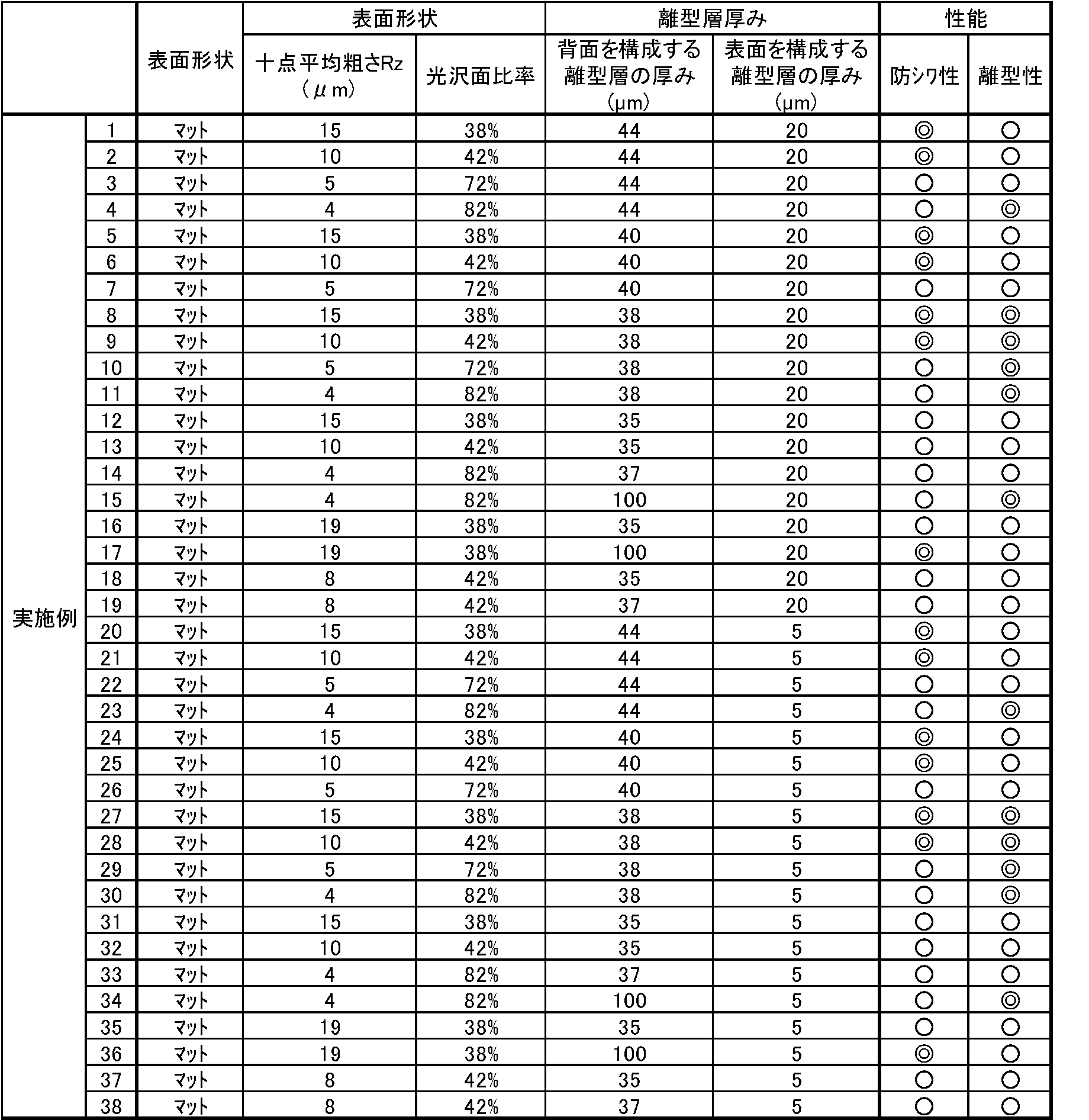
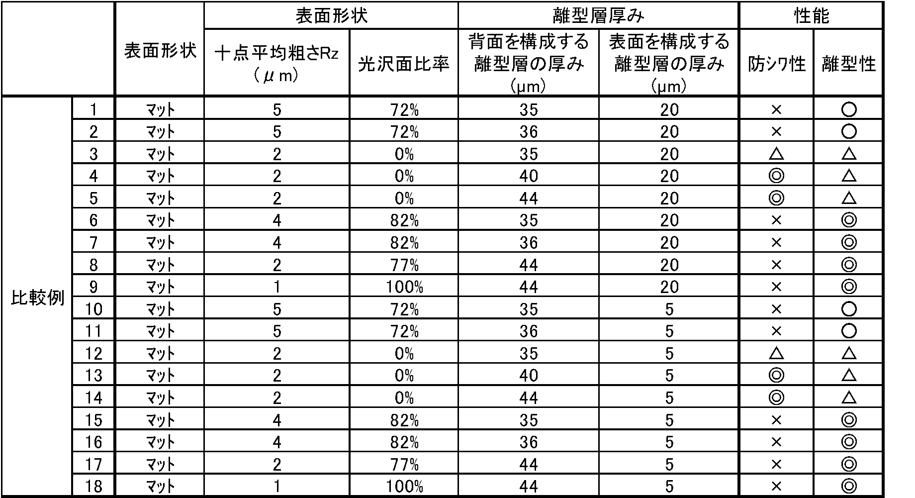
- Examples 1 to 38, Comparative Examples 1 to 18 A polybutylene terephthalate resin and a polypropylene resin are co-extruded and molded at a T die width of 400 mm using an extruder (GM Engineering Co., Ltd., GM30-28 (screw diameter 30 mm, L / D28)). Two polybutylene terephthalate resin layers having a thickness shown in Table 1 or 2 (a release layer constituting the back surface and a release layer constituting the surface) are laminated on the front and back of the polypropylene resin layer (intermediate layer), respectively. A three-layer resin film was obtained.
- the cooling roll with the pattern processed on the surface is pressed against the release surface of the release layer constituting the surface of the obtained three-layer resin film, and the processed pattern is transferred to the surface of the cooling roll.
- irregularities were formed on the release surface to obtain a release film.
- the release surface on which the irregularities are formed is the front surface, and the other release surface is the back surface.
- the surface and back surface roughened states of the obtained release film were confirmed with an optical microscope, the surface 10-point average roughness Rz was measured, and these results are shown in Table 1.
- the ten-point average roughness Rz on the back surface of each of the release films obtained in Examples and Comparative Examples was in the range of 1.0 to 3.0 ⁇ m.
- the FPC evaluation sample and the release film were taken out, peeled off the release film, and then the number of wrinkles transferred onto the coverlay surface was measured.
- the number of wrinkles was 0, it was “ ⁇ ”, when it was 1-10, “ ⁇ ”, when it was 11-20, “ ⁇ ”, 21 or more.
- the case was evaluated as “x”.
- the number of wrinkles is 20 or less, it can be said that it has sufficient wrinkle resistance as a release film at the time of manufacturing a flexible circuit board. More preferably, the number of wrinkles is 10 or less.
- the FPC evaluation sample and the release film were taken out and left on the desk, and the time until the release film was peeled off from the FPC evaluation sample was measured.
- the color tone seen from the release film side changes when air enters between the release film and the FPC evaluation sample from the state where the release film and the FPC evaluation sample are in close contact with each other. Therefore, the time from when the FPC evaluation sample and the release film were taken out to when the change in color tone was completed was defined as the time until the release film was peeled off.
- the time until the release film was peeled off was 30 seconds or less, “ ⁇ ”, when it exceeded 30 seconds but 60 seconds or less, “ ⁇ ”, when 60 seconds were exceeded but 90 seconds or less. In this case, “ ⁇ ” was assigned.
- time until a release film peels is 60 seconds or less, it can be said that it has mold release property sufficient as a release film at the time of manufacturing a flexible circuit board. More preferably, the time until the release film is peeled off is 30 seconds or less.
- ADVANTAGE OF THE INVENTION is a release film suitable for manufacture of a flexible circuit board, Comprising: The release film which can suppress generation
Landscapes
- Engineering & Computer Science (AREA)
- Microelectronics & Electronic Packaging (AREA)
- Laminated Bodies (AREA)
- Manufacture Of Macromolecular Shaped Articles (AREA)
- Non-Metallic Protective Coatings For Printed Circuits (AREA)
Abstract
Description
例えば、特許文献1には、ポリメチルペンテン樹脂を含む積層体からなる離型フィルムが記載されている。特許文献2には、表面粗さを定めたポリブチレンテレフタレートを含む厚みの薄い離型層とクッション層と副離型層とを有する離型フィルムが記載されている。特許文献3には、シンジオタクチックポリスチレン樹脂からなる離型層とクッション層とを有する離型フィルムが記載されている。
従って、離型フィルムに対してシワの発生を抑制できることが要求されているが、他の要求性能(例えば、埋め込み性、離型性等)を維持したままでシワの発生を抑制できる離型フィルムを得ることは困難であった。
以下、本発明を詳述する。
本発明の離型フィルムは、表面及び背面が粗面化されている。片面だけではなく、表面及び背面の両面が粗面化されていることにより、本発明の離型フィルムは、離型性を維持したままでシワの発生を抑制できるものとなる。
上記表面の十点平均粗さRzと、上記背面を構成する離型層の厚みとが上記範囲を満たすことにより、本発明の離型フィルムは、離型性を維持したままでシワの発生を抑制できるものとなる。上記表面の十点平均粗さRzが上記範囲より小さいと、離型フィルムにシワが多数発生してしまう。上記表面の十点平均粗さRzが上記範囲を超えると、離型フィルムの離型性が低下する。また、上記背面を構成する離型層の厚みが上記範囲より小さくても、離型フィルムにシワが多数発生してしまう。上記背面を構成する離型層の厚みの上限は特に限定されないが、好ましい上限は100μm、より好ましい上限は50μmである。
離型性を維持したままで効果的にシワの発生を抑制する観点から、上記表面の十点平均粗さRzが4μm以上20μm以下であり、かつ、上記背面を構成する離型層の厚みが37μm以上であるか、又は、上記表面の十点平均粗さRzが8μm以上15μm以下であり、かつ、上記背面を構成する離型層の厚みが35μm以上37μm未満であることがより好ましい。

図1に、実施例(いくつかの実施例を除く)及び比較例で得られた「表面の十点平均粗さRz」と、「背面を構成する離型層の厚み」とをプロットしたグラフを示す。図1では、本発明で規定する「表面の十点平均粗さRz」と、「背面を構成する離型層の厚み」との範囲を斜線で示す。ただし、「背面を構成する離型層の厚み」の上限は、図1の斜線で示される範囲に限定されない。
上記表面に模様が加工された冷却ロールを製造する方法は特に限定されず、例えば、平滑なロールの表面に凹模様を形成した後に、該ロールの平滑部分の粗さを調整する方法等が挙げられる。上記冷却ロール表面に加工された模様は特に限定されず、例えば、単一な形状の凹凸模様、大きなブラスト材による凹凸模様に細かな凹凸を重畳した複数の形状の凹凸模様等が挙げられる。
上記離型処理の方法は特に限定されず、例えば、上記表面及び/又は上記背面にシリコーン系、フッ素系等の離型剤を塗布又は散布する方法、熱処理、摩擦処理等を行う方法等の公知の方法を用いることができる。これらの離型処理は単独で用いてもよいし、2種以上が併用されてもよい。
上記結晶性芳香族ポリエステル樹脂は特に限定されず、例えば、ポリエチレンテレフタレート樹脂、ポリブチレンテレフタレート樹脂、ポリヘキサメチレンテレフタレート樹脂、ポリエチレンナフタレート樹脂、ポリブチレンナフタレート樹脂、テレフタル酸ブタンジオールポリテトラメチレングリコール共重合体等が挙げられる。これらの結晶性芳香族ポリエステル樹脂は単独で用いられてもよいし、2種以上が併用されてもよい。なかでも、非汚染性及び結晶性に優れることから、ポリブチレンテレフタレート樹脂が好適に用いられる。
上記ポリブチレンテレフタレート樹脂は特に限定されず、一般に用いられているものを使用することができ、具体的には例えば、ポリブチレンテレフタレートと脂肪族ポリエーテルとのブロック共重合体、ポリブチレンテレフタレートと脂肪族ポリエステルとのブロック共重合体等が挙げられる。これらのポリブチレンテレフタレート樹脂は単独で用いられてもよいし、2種以上が併用されてもよい。なかでも、耐熱性、離型性、フレキシブル回路基板の凹凸への追従性等のバランスの観点から、ポリブチレンテレフタレート樹脂に、ポリブチレンテレフタレートと脂肪族ポリエーテルとのブロック共重合体を混合した混合樹脂が好ましい。
上記表面を構成する離型層の厚みが1μm未満であると、離型フィルムにシワが発生することがある。上記表面を構成する離型層の厚みが20μmを超えると、離型フィルムの離型性が低下することがある。上記表面を構成する離型層の厚みのより好ましい下限は5μm、より好ましい上限は18μmである。
上記ポリオレフィン樹脂は特に限定されず、例えば、ポリエチレン樹脂や、ポリプロピレン樹脂や、エチレン-酢酸ビニル共重合体や、エチレン-メチルメタクリレート共重合体、エチレン-エチルアクリレート共重合体、エチレン-アクリル酸共重合体等のエチレン-アクリル系モノマー共重合体等が挙げられる。これらは単独で用いられてもよいし、2種以上が併用されてもよい。
上記中間層は、本発明の目的を阻害しない範囲で、更に、ポリスチレン、ポリ塩化ビニル、ポリアミド、ポリカーボネート、ポリスルフォン、ポリエステル等の樹脂を含有してもよい。
上記結晶性芳香族ポリエステル樹脂は特に限定されず、上述したような多層フィルムに含まれる結晶性芳香族ポリエステル樹脂と同じものが挙げられる。また、上述したような多層フィルムに含まれるポリブチレンテレフタレート樹脂と同じものが好適に用いられる。
本発明の離型フィルムが多層フィルムからなる場合、該多層フィルムを作製する方法は特に限定されず、例えば、水冷式又は空冷式共押出インフレーション法、共押出Tダイ法で製膜する方法、一方の離型層となるフィルムを作製した後、このフィルムに中間層を押出ラミネート法にて積層し、次いで他方の離型層をドライラミネーションする方法、一方の離型層となるフィルム、中間層となるフィルム及び他方の離型層となるフィルムをドライラミネーションする方法、溶剤キャスティング法、熱プレス成形法等が挙げられる。なかでも、各層の厚み制御に優れる点から、共押出Tダイ法で製膜する方法が好適である。
ポリブチレンテレフタレート樹脂とポリプロピレン樹脂とを押出機(ジーエムエンジニアリング社製、GM30-28(スクリュー径30mm、L/D28))を用いてTダイ幅400mmにて共押出して成形することにより、厚み65μmのポリプロピレン樹脂層(中間層)の表裏に、それぞれ表1又は2に示す厚みを有する2つのポリブチレンテレフタレート樹脂層(背面を構成する離型層、及び、表面を構成する離型層)が積層された3層樹脂フィルムを得た。
次いで、得られた3層樹脂フィルムの表面を構成する離型層の離型面に対して、表面に模様が加工された冷却ロールを押し当て、冷却ロール表面に加工された模様を転写させることにより離型面に凹凸を形成し、離型フィルムを得た。なお、凹凸を形成した離型面が表面、他方の離型面が背面である。得られた離型フィルムの表面及び背面の粗面化状態を光学顕微鏡により確認し、表面の十点平均粗さRzを測定して、これらの結果を表1に示した。なお、実施例及び比較例で得られた離型フィルムそれぞれの背面の十点平均粗さRzは1.0~3.0μmの範囲内であった。
実施例1~38及び比較例1~18で得られた離型フィルムについて以下の評価を行った。結果を表1又は2に示した。
離型フィルム表面を光学顕微鏡(キーエンス社製、レーザーマイクロスコープVK8710)を用いて20倍に拡大して観察した。観察視野(700μm×525μm)における平滑面の面積を測り、観察視野に占める平滑面の面積の百分率を求め、得られた値を光沢面比率(%)とした。なお、光沢面比率が38%、42%、72%、82%、77%、0%であった離型フィルム表面の光学顕微鏡写真をそれぞれ図2~7に示した。
CCL(20cm×20cm、ポリイミド厚25μm、銅箔35μm)、カバーレイ(20cm×20cm、ポリイミド厚15μm、エポキシ系樹脂接着剤層25μm)、及び、離型フィルムを下からこの順番に積み上げ、スライド式真空ヒータプレス(MKP-3000V-WH-ST、ミカドテクノス社製)を用いて予め180℃で加熱したプレス金型間に置いて位置合わせをした後、プレスを開始し(設置から実際に圧力がかかるまでに約10秒)、真空条件下、50kg/cm2で2分間プレスすることにより、CCLとカバーレイとからなるフレキシブル回路基板(FPC)評価サンプルを作製した。
その後、FPC評価サンプル及び離型フィルムを取り出し、離型フィルムを剥がした後、カバーレイ表面上に転写されたシワの個数を測定した。シワの個数が0個であった場合を「◎」と、1~10個であった場合を「○」と、11~20個であった場合を「△」と、21個以上であった場合を「×」と評価した。
なお、シワの個数が20個以内の場合には、フレキシブル回路基板を製造する際の離型フィルムとして充分な防シワ性を有するといえる。より好ましくは、シワの個数が10個以内である。
CCL(20cm×20cm、ポリイミド厚25μm、銅箔35μm)、カバーレイ(20cm×20cm、ポリイミド厚25μm、エポキシ系樹脂接着剤層35μm)、及び、離型フィルムを下からこの順番に積み上げ、スライド式真空ヒータプレス(MKP-3000V-WH-ST、ミカドテクノス社製)を用いて予め180℃で加熱したプレス金型間に置いて位置合わせをした後、プレスを開始し(設置から実際に圧力がかかるまでに約10秒)、50kg/cm2で2分間プレスすることにより、CCLとカバーレイとからなるFPC評価サンプルを作製した。
その後、FPC評価サンプル及び離型フィルムを取り出し、机上に放置し、離型フィルムがFPC評価サンプルから剥がれるまでの時間を計測した。具体的には、離型フィルムとFPC評価サンプルとが密着している状態から、離型フィルムとFPC評価サンプルとの間に空気が入っていくことにより、離型フィルム側から見た色調が変わるため、FPC評価サンプル及び離型フィルムを取り出した時点から、色調の変化が完了した時点までの時間を離型フィルムが剥がれるまでの時間とした。
離型フィルムが剥がれるまでの時間が30秒以下であった場合を「◎」と、30秒は超えるが60秒以下であった場合を「○」と、60秒は超えるが90秒以下であった場合を「△」とした。
なお、離型フィルムが剥がれるまでの時間が60秒以下の場合には、フレキシブル回路基板を製造する際の離型フィルムとして充分な離型性を有するといえる。より好ましくは、離型フィルムが剥がれるまでの時間が30秒以下である。
Claims (9)
- フレキシブル回路基板の製造に適した離型フィルムであって、
表面及び背面が粗面化されており、
前記表面の十点平均粗さRzが4μm以上20μm以下であり、かつ、前記背面を構成する離型層の厚みが35μm以上である(ただし、前記表面の十点平均粗さRzが4μm以上5μm以下であり、かつ、前記背面を構成する離型層の厚みが35μm以上36μm以下である場合を除く)
ことを特徴とする離型フィルム。 - 表面の光沢面比率が35%以上85%以下であることを特徴とする請求項1記載の離型フィルム。
- 表面及び背面をそれぞれ構成する2つの離型層と、中間層とを有する多層フィルムからなることを特徴とする請求項1又は2記載の離型フィルム。
- 表面及び背面をそれぞれ構成する2つの離型層のうち、表面を構成する離型層がポリブチレンテレフタレート樹脂を含有することを特徴とする請求項3記載の離型フィルム。
- 表面を構成する離型層の厚みが1μm以上20μm以下であることを特徴とする請求項3又は4記載の離型フィルム。
- 表面及び背面を構成する1つの離型層のみからなる単層フィルムであることを特徴とする請求項1又は2記載の離型フィルム。
- 表面及び背面を構成する1つの離型層がポリブチレンテレフタレート樹脂を含有することを特徴とする請求項6記載の離型フィルム。
- 表面の十点平均粗さRzが4μm以上20μm以下であり、かつ、背面を構成する離型層の厚みが37μm以上であるか、又は、表面の十点平均粗さRzが8μm以上15μm以下であり、かつ、背面を構成する離型層の厚みが35μm以上37μm未満であることを特徴とする請求項1又は2記載の離型フィルム。
- 表面及び背面をそれぞれ構成する2つの離型層の合計厚みが、離型フィルムの厚みのうち半分を超える厚みを占めることを特徴とする請求項3記載の離型フィルム。
Priority Applications (3)
| Application Number | Priority Date | Filing Date | Title |
|---|---|---|---|
| CN201911003268.XA CN110602896B (zh) | 2013-08-05 | 2014-07-31 | 脱模膜 |
| KR1020157033856A KR102264950B1 (ko) | 2013-08-05 | 2014-07-31 | 이형 필름 |
| CN201480037650.1A CN105359634B (zh) | 2013-08-05 | 2014-07-31 | 脱模膜 |
Applications Claiming Priority (4)
| Application Number | Priority Date | Filing Date | Title |
|---|---|---|---|
| JP2013-162657 | 2013-08-05 | ||
| JP2013162657 | 2013-08-05 | ||
| JP2014-121820 | 2014-06-12 | ||
| JP2014121820A JP6223913B2 (ja) | 2013-08-05 | 2014-06-12 | 離型フィルム |
Publications (1)
| Publication Number | Publication Date |
|---|---|
| WO2015019933A1 true WO2015019933A1 (ja) | 2015-02-12 |
Family
ID=52461269
Family Applications (1)
| Application Number | Title | Priority Date | Filing Date |
|---|---|---|---|
| PCT/JP2014/070192 Ceased WO2015019933A1 (ja) | 2013-08-05 | 2014-07-31 | 離型フィルム |
Country Status (5)
| Country | Link |
|---|---|
| JP (1) | JP6223913B2 (ja) |
| KR (1) | KR102264950B1 (ja) |
| CN (2) | CN105359634B (ja) |
| TW (2) | TWI650246B (ja) |
| WO (1) | WO2015019933A1 (ja) |
Families Citing this family (5)
| Publication number | Priority date | Publication date | Assignee | Title |
|---|---|---|---|---|
| JP6223913B2 (ja) * | 2013-08-05 | 2017-11-01 | 積水化学工業株式会社 | 離型フィルム |
| JP6391554B2 (ja) * | 2015-12-14 | 2018-09-19 | 住友ベークライト株式会社 | 離型フィルム |
| WO2021060154A1 (ja) * | 2019-09-25 | 2021-04-01 | 積水化学工業株式会社 | 離型フィルム及び離型フィルムの製造方法 |
| CN113840707A (zh) * | 2019-09-25 | 2021-12-24 | 积水化学工业株式会社 | 脱模膜 |
| JP6977848B1 (ja) * | 2020-11-02 | 2021-12-08 | 住友ベークライト株式会社 | 離型フィルムおよび成型品の製造方法 |
Citations (4)
| Publication number | Priority date | Publication date | Assignee | Title |
|---|---|---|---|---|
| WO2009038118A1 (ja) * | 2007-09-21 | 2009-03-26 | Sekisui Chemical Co., Ltd. | 離型フィルム |
| JP2009111432A (ja) * | 2009-02-16 | 2009-05-21 | Panasonic Electric Works Co Ltd | 片面板の製造方法及びプリント配線板の製造方法 |
| JP2009241410A (ja) * | 2008-03-31 | 2009-10-22 | Sumitomo Bakelite Co Ltd | 離型フィルム |
| WO2011111826A1 (ja) * | 2010-03-12 | 2011-09-15 | 積水化学工業株式会社 | 離型フィルム及び離型フィルムの製造方法 |
Family Cites Families (8)
| Publication number | Priority date | Publication date | Assignee | Title |
|---|---|---|---|---|
| TWI476103B (zh) * | 2003-07-01 | 2015-03-11 | Sumitomo Bakelite Co | A release film and a method of manufacturing a flexible printed wiring board using the release film |
| JP2005122147A (ja) | 2003-09-24 | 2005-05-12 | Fuji Photo Film Co Ltd | 反射防止フィルム、その製造方法、偏光板および画像表示装置 |
| JP2005246836A (ja) | 2004-03-05 | 2005-09-15 | Konica Minolta Photo Imaging Inc | インクジェット記録用紙 |
| KR100927514B1 (ko) | 2005-05-13 | 2009-11-17 | 미쓰이 가가쿠 가부시키가이샤 | 4-메틸-1-펜텐계 중합체를 포함하는 적층체 및 이것으로이루어진 이형 필름 |
| KR101485213B1 (ko) * | 2007-07-31 | 2015-01-22 | 스미또모 베이크라이트 가부시키가이샤 | 이형 필름 |
| JP5557152B2 (ja) | 2010-02-09 | 2014-07-23 | 住友ベークライト株式会社 | 積層フィルム |
| JP5653123B2 (ja) * | 2010-08-17 | 2015-01-14 | ユニチカ株式会社 | 離型用シート |
| JP6223913B2 (ja) * | 2013-08-05 | 2017-11-01 | 積水化学工業株式会社 | 離型フィルム |
-
2014
- 2014-06-12 JP JP2014121820A patent/JP6223913B2/ja active Active
- 2014-07-31 KR KR1020157033856A patent/KR102264950B1/ko active Active
- 2014-07-31 CN CN201480037650.1A patent/CN105359634B/zh active Active
- 2014-07-31 CN CN201911003268.XA patent/CN110602896B/zh active Active
- 2014-07-31 WO PCT/JP2014/070192 patent/WO2015019933A1/ja not_active Ceased
- 2014-08-04 TW TW103126557A patent/TWI650246B/zh active
- 2014-08-04 TW TW107135256A patent/TWI666123B/zh active
Patent Citations (4)
| Publication number | Priority date | Publication date | Assignee | Title |
|---|---|---|---|---|
| WO2009038118A1 (ja) * | 2007-09-21 | 2009-03-26 | Sekisui Chemical Co., Ltd. | 離型フィルム |
| JP2009241410A (ja) * | 2008-03-31 | 2009-10-22 | Sumitomo Bakelite Co Ltd | 離型フィルム |
| JP2009111432A (ja) * | 2009-02-16 | 2009-05-21 | Panasonic Electric Works Co Ltd | 片面板の製造方法及びプリント配線板の製造方法 |
| WO2011111826A1 (ja) * | 2010-03-12 | 2011-09-15 | 積水化学工業株式会社 | 離型フィルム及び離型フィルムの製造方法 |
Also Published As
| Publication number | Publication date |
|---|---|
| KR20160039151A (ko) | 2016-04-08 |
| TWI650246B (zh) | 2019-02-11 |
| CN105359634A (zh) | 2016-02-24 |
| TW201509684A (zh) | 2015-03-16 |
| CN105359634B (zh) | 2019-11-12 |
| CN110602896B (zh) | 2023-01-03 |
| KR102264950B1 (ko) | 2021-06-14 |
| TWI666123B (zh) | 2019-07-21 |
| JP2015052099A (ja) | 2015-03-19 |
| JP6223913B2 (ja) | 2017-11-01 |
| CN110602896A (zh) | 2019-12-20 |
| TW201902687A (zh) | 2019-01-16 |
Similar Documents
| Publication | Publication Date | Title |
|---|---|---|
| JP4332204B2 (ja) | 離型フィルム | |
| JP6223913B2 (ja) | 離型フィルム | |
| TWI540051B (zh) | Release film | |
| WO2020040240A1 (ja) | 離型フィルムおよび成型品の製造方法 | |
| JP6014680B2 (ja) | 積層フィルム及びシールドプリント配線板 | |
| JP6908658B2 (ja) | 離型フィルム | |
| JP2010149520A (ja) | 離型フィルム及びこれを用いたフレキシブルプリント配線板の製造法 | |
| CN116133848B (zh) | 脱模膜及成型品的制造方法 | |
| WO2017169654A1 (ja) | 離型フィルムおよび成型品の製造方法 | |
| JP2009241410A (ja) | 離型フィルム | |
| JPWO2014141512A1 (ja) | 離型フィルム | |
| KR102301255B1 (ko) | 이형 필름 | |
| JP5438367B2 (ja) | 多層離型フィルム | |
| JP5718609B2 (ja) | マスキングフィルム支持体 | |
| JP2010194841A (ja) | 離型フィルム及びその製造方法 | |
| JP5231913B2 (ja) | 離型フィルム | |
| JP7243258B2 (ja) | 離型フィルム | |
| JP7619505B1 (ja) | 離型フィルムおよび成型品の製造方法 | |
| JP7619507B1 (ja) | 離型フィルムおよび成型品の製造方法 | |
| JP7619506B1 (ja) | 離型フィルムおよび成型品の製造方法 | |
| JP2006212954A (ja) | 離型フィルム | |
| JP2025070583A (ja) | 延伸ポリオレフィンフィルム及びその製造方法、ビルドアップフィルム用保護フィルム | |
| WO2025205736A1 (ja) | 離型フィルムおよび成型品の製造方法 | |
| JP2008030246A (ja) | 片面金属箔張り積層板およびそれを用いたプリント配線板 |
Legal Events
| Date | Code | Title | Description |
|---|---|---|---|
| WWE | Wipo information: entry into national phase |
Ref document number: 201480037650.1 Country of ref document: CN |
|
| 121 | Ep: the epo has been informed by wipo that ep was designated in this application |
Ref document number: 14835207 Country of ref document: EP Kind code of ref document: A1 |
|
| ENP | Entry into the national phase |
Ref document number: 20157033856 Country of ref document: KR Kind code of ref document: A |
|
| NENP | Non-entry into the national phase |
Ref country code: DE |
|
| 122 | Ep: pct application non-entry in european phase |
Ref document number: 14835207 Country of ref document: EP Kind code of ref document: A1 |