WO2014196401A1 - 測定対象物の厚さ計測方法 - Google Patents
測定対象物の厚さ計測方法 Download PDFInfo
- Publication number
- WO2014196401A1 WO2014196401A1 PCT/JP2014/063859 JP2014063859W WO2014196401A1 WO 2014196401 A1 WO2014196401 A1 WO 2014196401A1 JP 2014063859 W JP2014063859 W JP 2014063859W WO 2014196401 A1 WO2014196401 A1 WO 2014196401A1
- Authority
- WO
- WIPO (PCT)
- Prior art keywords
- measurement
- light
- thickness
- dielectric layer
- wavelength
- Prior art date
- Legal status (The legal status is an assumption and is not a legal conclusion. Google has not performed a legal analysis and makes no representation as to the accuracy of the status listed.)
- Ceased
Links
Images













Classifications
-
- G—PHYSICS
- G01—MEASURING; TESTING
- G01B—MEASURING LENGTH, THICKNESS OR SIMILAR LINEAR DIMENSIONS; MEASURING ANGLES; MEASURING AREAS; MEASURING IRREGULARITIES OF SURFACES OR CONTOURS
- G01B11/00—Measuring arrangements characterised by the use of optical techniques
- G01B11/02—Measuring arrangements characterised by the use of optical techniques for measuring length, width or thickness
- G01B11/06—Measuring arrangements characterised by the use of optical techniques for measuring length, width or thickness for measuring thickness ; e.g. of sheet material
- G01B11/0616—Measuring arrangements characterised by the use of optical techniques for measuring length, width or thickness for measuring thickness ; e.g. of sheet material of coating
- G01B11/0675—Measuring arrangements characterised by the use of optical techniques for measuring length, width or thickness for measuring thickness ; e.g. of sheet material of coating using interferometry
-
- G—PHYSICS
- G01—MEASURING; TESTING
- G01B—MEASURING LENGTH, THICKNESS OR SIMILAR LINEAR DIMENSIONS; MEASURING ANGLES; MEASURING AREAS; MEASURING IRREGULARITIES OF SURFACES OR CONTOURS
- G01B11/00—Measuring arrangements characterised by the use of optical techniques
- G01B11/02—Measuring arrangements characterised by the use of optical techniques for measuring length, width or thickness
- G01B11/06—Measuring arrangements characterised by the use of optical techniques for measuring length, width or thickness for measuring thickness ; e.g. of sheet material
- G01B11/0616—Measuring arrangements characterised by the use of optical techniques for measuring length, width or thickness for measuring thickness ; e.g. of sheet material of coating
- G01B11/0625—Measuring arrangements characterised by the use of optical techniques for measuring length, width or thickness for measuring thickness ; e.g. of sheet material of coating with measurement of absorption or reflection
-
- G—PHYSICS
- G01—MEASURING; TESTING
- G01B—MEASURING LENGTH, THICKNESS OR SIMILAR LINEAR DIMENSIONS; MEASURING ANGLES; MEASURING AREAS; MEASURING IRREGULARITIES OF SURFACES OR CONTOURS
- G01B9/00—Measuring instruments characterised by the use of optical techniques
- G01B9/02—Interferometers
- G01B9/0209—Low-coherence interferometers
- G01B9/02091—Tomographic interferometers, e.g. based on optical coherence
Definitions
- the substrate is mounted on an electrostatic chuck (ESC) provided on the mounting table.
- the electrostatic chuck has a configuration in which a conductive sheet-like electrode layer is sandwiched between dielectric layers (see, for example, Patent Document 1).
- the substrate is attracted to the electrostatic chuck by a Coulomb force generated by applying a voltage from the DC voltage source to the electrode layer.
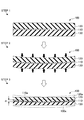
- an electrostatic chuck As an example of manufacturing an electrostatic chuck, as shown in STEP 1 of FIG. 1, a method of sintering in a state where the front and back of the electrode layer 110 are sandwiched and laminated by the dielectric layers 120 and 130 is used. Many. When ceramic is used for the dielectric layers 120 and 130, as shown in STEP2 of FIG. 1, the electrostatic chuck 100 is subjected to high-temperature processing in a state where pressure is applied during sintering. For this reason, the electrostatic chuck 100 may be distorted by pressure, thermal stress, or the like. After sintering, as shown in STEP 3 of FIG. 1, the front and back surfaces of the electrostatic chuck 100 are polished and flattened.
- the thickness of the dielectric layers 120 and 130 is required for high uniformity.
- the heat capacity is increased, so that the thermal response is deteriorated and the temperature controllability of the substrate is deteriorated.
- the electrostatic force is weak, a sufficient adsorption force cannot be obtained on the substrate, which causes the substrate to jump from the electrostatic chuck 100 particularly when the pressure of the heat transfer gas supplied to the back surface of the substrate is high. .
- the thickness of the dielectric layers 120 and 130 is thinner than the design value, sufficient mechanical strength cannot be obtained for the electrostatic chuck 100.
- the insulation is not sufficient, dielectric breakdown may occur, and leakage current and abnormal discharge may occur.
- an object of one aspect is to accurately measure the thickness of a measurement object in a non-contact manner.
- a method for measuring a thickness of a measurement object having a first main surface and a second main surface opposite to the first main surface A first step of outputting measurement light having a wavelength that passes through the measurement object from a light source; The collimator or the focuser is moved, the measurement light output from the collimator or the focuser is emitted to the measurement position of the first main surface of the measurement object, and the reflected light from the first main surface and the second main surface
- a second step of entering the collimator or focuser A third step in which the reflected light from the collimator or the focuser is incident on the light receiving element, the intensity of the light incident on the light receiving element is acquired, and the wavelength of the light incident on the light receiving element is swept; Using the acquired intensity of the light and the wavelength of the swept light, an intensity distribution that depends on the wavelength and is an intensity distribution of reflected light from the first main surface and the second main surface is obtained.
- the thickness of the measurement object can be accurately measured without contact.
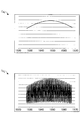
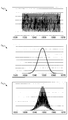
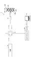
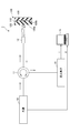
- FIG. 1 is an overall configuration diagram of an optical interference system according to an embodiment. It is a functional block diagram of the arithmetic unit shown in FIG. It is a graph which shows an example of the relationship between the applied voltage and transmission wavelength in a wavelength conversion filter. “A” is a time sampling of voltage, “b” is a time sampling of light intensity, and “c” is a graph showing an example of a relationship between light intensity and voltage. It is an example of a wavelength-intensity spectrum when a wavelength conversion filter is used. It is a schematic diagram explaining an incident light spectrum and a reflected light spectrum. It is a schematic diagram explaining the Fourier transform of a reflected light spectrum.
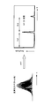
- A is a spectrum indicating a position-dependent intensity distribution.
- B is a spectrum indicating an intensity distribution depending on the wave number.
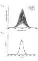
- A is an example of a reflected light spectrum.
- B is a peak waveform after FFT of the reflected light spectrum shown in “a”.
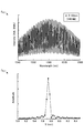
- A is an example of a reflected light spectrum.
- B is a peak waveform after FFT of the reflected light spectrum shown in “a”.
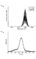
- A is an example of a reflected light spectrum.
- B is a peak waveform after FFT of the reflected light spectrum shown in “a”.
- A” is an example of a reflected light spectrum.
- B is a peak waveform after FFT of the reflected light spectrum shown in “a”.
- A” and “b” are examples of Gaussian functions.
- C is a schematic diagram illustrating a Gaussian function necessary for suitably calculating the center of gravity.
- A is an example of a reflected light spectrum.
- B is an example of a Gaussian function.
- C is a spectrum obtained by adjusting the reflected light spectrum indicated by “a” with the Gaussian function indicated by “b”.
- A is an example of a reflected light spectrum.
- B is a waveform after FFT.
- C is a partially enlarged view of the waveform shown in “b”.
- A” is an example of a reflected light spectrum.
- B is a waveform after FFT.
- C is a partially enlarged view of the waveform shown in “b”.
- A is a light source spectrum showing an intensity distribution depending on the wavelength.
- B is a reflected light spectrum showing an intensity distribution depending on the wavelength.
- C is a reflected light spectrum showing an intensity distribution depending on the reciprocal of the wavelength. It is a graph for demonstrating operation
- A” is a spectrum obtained by linearly interpolating the reflected light spectrum indicating the intensity distribution depending on the reciprocal of the wavelength.
- “B” is a spectrum obtained by fast Fourier transform of the reflected light spectrum of “a”.
- “C” is a partially enlarged view of “b”. It is a figure for demonstrating the dot shape and incident light of an electrostatic chuck surface. It is the figure which showed the thickness measurement result at the time of making light enter from one point in a dot. It is the figure which showed the thickness measurement result at the time of making light inject from several points in a dot. It is a figure for demonstrating the case where light is entered using a focuser. It is the figure which showed the abnormal discharge generation
- A shows the measurement result of the thickness in the diameter direction of the dielectric layer
- b shows the measurement result of the thickness in the circumferential direction.
- A is an example of the spectrum of the measurement light of the light source spectrum.
- B is an example of a reflected light spectrum.
- A is an example of reflectance.
- B is an example of a Gaussian function.
- C is an example of the reflected light spectrum after adjustment. It is a functional block diagram which shows the other example of an optical interference system. It is a functional block diagram which shows the other example of an optical interference system. It is a functional block diagram which shows the other example of an optical interference system. It is a functional block diagram which shows the other example of an optical interference system.
- the thickness of the dielectric layers 120 and 130 is thinner than the design value, sufficient mechanical strength cannot be obtained for the electrostatic chuck 100.
- the insulation is not sufficient, dielectric breakdown may occur, and leakage current and abnormal discharge may occur.
- the uniformity of the thickness of the dielectric layers 120 and 130 leads to the performance of the electrostatic chuck 100 being good or bad.
- internal distortion may occur due to pressure or thermal stress applied to the electrostatic chuck 100 during sintering (STEP 2 in FIG. 1).
- the surfaces 120a and 130a of the dielectric layers 120 and 130 are polished in a state where there is distortion, the surfaces 120a and 130a of the dielectric layers 120 and 130 become flat.
- the thickness of the dielectric layers 120 and 130 becomes non-uniform due to the internal strain of the electrostatic chuck 100 (STEP 3 in FIG. 1).
- the distance from the surface 120a of the dielectric layer 120 to the surface 110a of the electrode layer 110 is set with high accuracy and non-uniformity. A method of measuring by destruction is desired. Further, when measuring the thickness of the dielectric layer, it is preferable to measure the thickness without contact from the viewpoint of preventing particles and contamination.
- the thickness of the dielectric layer there is a method of calculating from a measured value of capacitance.
- the measurement probe contacts the surface of the dielectric layer, particles and metal contamination may occur.
- an error occurs in the numerical value measured by the pressing pressure of the probe.
- the electrostatic chuck 100 since the electrostatic chuck 100 has a laminated structure and is flattened by polishing (see STEP 3 in FIG. 1) at the time of manufacture, the electrostatic chuck 100 is only measured by measuring the entire thickness of the electrostatic chuck 100. It is not possible to measure the distortion occurring inside.
- the thickness of the dielectric layer In other words, it must be equal to or greater than “the lower limit thickness at which the dielectric layer causes dielectric breakdown” and less than “the upper limit thickness at which the substrate can be attracted by the electrostatic chuck”.
- the numerical value from the surface 110a of the electrode layer 110 to the surface 120a of the dielectric layer 120 is about several hundred ⁇ m. More desirably, it is about 200 ⁇ m or more and 400 ⁇ m or less. Therefore, the allowable range of the strain ⁇ of the electrode layer 110 shown in STEP 3 of FIG. 1 needs to be measured with a resolution of ⁇ m order.
- the method for measuring the thickness of the dielectric layer requires high-precision resolution, and it is difficult to calculate the thickness of the dielectric layer from the measured capacitance value.
- this embodiment proposes a method for optically measuring the thickness of the dielectric layer. Thereby, it is possible to measure the dielectric layer with high accuracy and non-contact.
- a method for measuring the thickness of the dielectric layer according to the present embodiment will be described.
- FIG. 2 is an overall configuration diagram of an optical interference system according to an embodiment.
- the optical interference system 1 is a system that executes a method for measuring the thickness of a dielectric layer according to an embodiment.
- the optical interference system 1 measures the thickness of the measurement object using OCT (Optical Coherence Tomography).
- the optical interference system 1 includes a light source 10, an optical circulator 11, a collimator 12, a tunable filter 40, a light receiving element 41, an A / D conversion unit 42, a wavelength control unit 43, and a calculation device 15.
- Each of the light source 10, the optical circulator 11, the collimator 12, the tunable filter 40, and the light receiving element 41 is connected by an optical fiber cable.
- the light source 10 outputs measurement light having a wavelength that passes through the dielectric layer 120 that is the measurement object of the present embodiment.
- the light source 10 for example, an SLD (Super Luminescent Diode) is used.
- the dielectric layer 120 has a plate shape, for example, and has a front surface 120a and a back surface 120b.
- the back surface 120 b is a contact surface with the electrode layer 110.
- the thickness of the dielectric layer used in the electrostatic chuck 100 is measured as an example of the measurement object.
- Other examples of the measurement object include, for example, Si (silicon) in addition to a dielectric such as SiO 2 (quartz) or Al 2 O 3 (sapphire).
- the front surface 120a of the dielectric layer 120 is an example of a first main surface of the measurement object, and the back surface 120b of the dielectric layer 120 is an example of a second main surface facing the first main surface of the measurement object. .
- the optical circulator 11 is connected to the light source 10, the collimator 12 and the tunable filter 40.
- the optical circulator 11 emits measurement light generated by the light source 10 to the collimator 12.
- a 2 ⁇ 1 or 2 ⁇ 2 photocoupler may be used.
- the collimator 12 emits the measurement light adjusted as parallel rays to the dielectric layer 120.
- the measurement light passes through the dielectric layer from the front surface 120a of the dielectric layer 120 and is reflected by the back surface 120b (contact surface with the electrode layer) of the dielectric layer 120.
- the collimator 12 receives the reflected light from the dielectric layer 120.
- the reflected light includes not only reflected light from the front surface 120a but also reflected light from the back surface 120b.
- the collimator 12 emits the reflected light to the optical circulator 11.
- the optical circulator 11 emits reflected light to the tunable filter 40.
- a focuser may be used instead of the collimator 12. The case where it is preferable to use the focuser will be described later.
- the tunable filter 40 is a wavelength tunable filter that can change the wavelength of input light.
- the tunable filter 40 can be any filter that can control the wavelength of transmitted light that has passed through the filter by controlling the applied voltage and applied frequency, such as the Fabry-Perot method, diffraction grating method, interference filter method, and acousto-optic method. Good.
- the applied voltage and applied frequency are controlled by a wavelength control unit 43 described later.
- the tunable filter 40 emits transmitted light to the light receiving element 41.
- the light receiving element 41 is an element that detects light, and outputs a signal corresponding to the intensity of light, for example.
- a single light receiving element 41 is used.
- the light receiving element 41 for example, a photodiode or a photomultiplier tube is used.
- the light receiving element 41 outputs an output signal to the A / D converter 42.
- the A / D converter 42 converts the analog output signal of the light receiving element 41 into a digital signal.
- the A / D conversion timing is controlled by the wavelength controller 43.
- the A / D converter 42 outputs a digital signal to the arithmetic device 15.
- the arithmetic device 15 is an example of a control unit realized by a device such as a PC.
- the wavelength controller 43 is connected to the tunable filter 40 and controls the voltage applied to the tunable filter 40.
- the wavelength controller 43 is connected to the A / D converter 42 and synchronizes the applied voltage control timing with the A / D conversion timing.
- the reflected light spectrum (interference intensity distribution) of the reflected light is measured by the tunable filter 40, the light receiving element 41, the A / D conversion unit 42, and the wavelength control unit 43.
- the reflected light spectrum shows an intensity distribution depending on the wavelength or frequency of the reflected light.
- the digital signal output from the A / D conversion unit 42 to the arithmetic device 15 becomes a reflected light spectrum.
- the arithmetic unit 15 measures the thickness of the dielectric layer 120 based on the reflected light spectrum.
- FIG. 3 is a functional block diagram of the arithmetic device 15. As illustrated in FIG. 3, the arithmetic device 15 includes a normalization unit 30, a waveform adjustment unit 31, an optical path length calculation unit 16, and a thickness calculation unit 20.
- the normalization unit 30 normalizes the waveform of the reflected light spectrum using the spectrum of the measurement light of the light source 10 acquired in advance. For example, when the profile of the light source spectrum (measurement light spectrum) of the light source 10 is distorted or asymmetric, the signal after processing described later is also distorted, and as a result, high-accuracy measurement cannot be performed. There is a fear. For this reason, the reflected light spectrum is normalized by dividing it by the light source spectrum. That is, the reflectance waveform. The normalization unit 30 outputs the calculated waveform to the waveform adjustment unit 31.
- the waveform adjustment unit 31 adjusts the waveform using a window function depending on the wavelength.
- the window function is a bell-shaped function that maximizes the center wavelength determined by the wavelength sweep range by the sweep unit and gradually attenuates as the difference from the center wavelength increases.
- the center wavelength for example, the median value of the wavelength sweep range is adopted.
- the window function a Gaussian function, a Lorentz function, a composite function of a Gaussian function and a Lorentz function, or the like is used.
- the waveform adjustment unit 31 applies the window function to the reflectance waveform output by the normalization unit 30.
- the waveform adjustment unit 31 outputs the adjusted waveform to the optical path length calculation unit 16.
- the optical path length calculation unit 16 includes a Fourier transform unit 17, a data interpolation unit 18, and a centroid calculation unit 19.
- the Fourier transform unit 17 performs Fourier transform on the reflected light spectrum by fast Fourier transform (FFT: Fast Fourier Transform).
- FFT Fast Fourier Transform
- the reflected light spectrum indicating the intensity distribution depending on the frequency (frequency per unit time) is converted into the reflected light spectrum indicating the time-dependent intensity distribution.
- a reflected light spectrum indicating an intensity distribution depending on a spatial frequency (frequency per unit length) is converted into a reflected light spectrum indicating a position-dependent intensity distribution. .
- the data interpolation unit 18 interpolates data points in a range including a predetermined peak value of the reflected light spectrum after Fourier transform.
- the centroid calculation unit 19 calculates the centroid position of a predetermined peak value of the reflected light spectrum after Fourier transform.
- the optical path length calculation unit 16 calculates the optical path length based on the position of the center of gravity.
- the thickness calculator 20 calculates the thickness of the measurement target by dividing the optical path length by the refractive index of the material of the measurement target.
- the refractive index of Al 2 O 3 is 1.8 at a wavelength of 1 ⁇ m.
- the refractive index of Si is 3.4 at a wavelength of 4 ⁇ m.
- the refractive index of SiO 2 is 1.5 at a wavelength of 1 ⁇ m.
- the normalization unit 30 may not be provided when the light source spectrum falls within the measurement wavelength range.
- the waveform adjustment unit 31 applies a window function to the digital signal output from the A / D conversion unit 42.
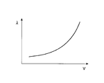
- FIG. 4 is a graph showing the relationship between the applied voltage and the transmission wavelength in the tunable filter 40.
- the relationship between the applied voltage and the wavelength of transmitted light is acquired in advance.
- the A / D converter 42 performs time sampling.
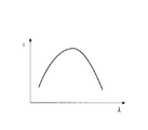
- “A” in FIG. 5 is a time-sampling graph with respect to the voltage V
- “b” in FIG. 5 is a time-sampling graph with respect to the light intensity I. Based on “a” in FIG.
- FIG. 6 is an example of an optical spectrum.
- FIG. 7 is a schematic diagram for explaining the incident light spectrum and the reflected light spectrum.
- the measurement light from the light source 10 is incident light.
- the intensity S (k) of the incident light spectrum depends on the spatial frequency 1 / ⁇ (frequency per unit length).
- the wavelength of the light source 10 is ⁇
- the wave number k is 2 ⁇ / ⁇ .
- the thickness of the dielectric layer 120 is d, the refractive index is n, and the reflectance is R.
- the reflected light E is obtained by superimposing a plurality of reflection components.
- E1 is a reflection component on the surface 120a.
- E2 is a reflection component on the back surface 120b.
- E3 is a reflection component reflected once by the front surface 120a and twice by the back surface 120b. Note that reflection components after E4 are omitted.
- a plurality of components overlap to obtain the intensity I (k) of the reflected light spectrum.
- the intensity I (k) of the reflected light spectrum has a relationship expressed by the following formula with the intensity S (k) of the incident light spectrum.
- the second term is a front-back interference term.
- the third term is a front-back multiple interference term.
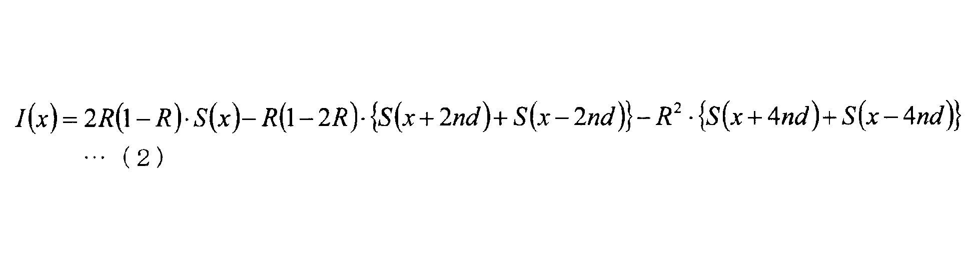
- FIG. 8 is a schematic diagram for explaining the Fourier transform of the reflected light spectrum I (k). As shown in FIG. 8, the spatial frequency 1 / ⁇ is converted into a position x by a spatial domain Fourier transform. The intensity I (x) of the reflected light spectrum converted to the position x is as follows by performing Fourier transform on Equation 1.
- a peak value appears every 2nd.
- 2nd is the optical path difference between the front and back surfaces. That is, nd is the optical path length between the front and back surfaces of the dielectric layer.
- the thickness of the dielectric layer can be calculated based on the optical path length nd.
- the spatial domain Fourier transform is used, but a time domain Fourier transform may be used.
- the position x satisfies the following relationship.
- FIG. 9 is a schematic diagram illustrating reflected light.
- the front surface position is 0 and the back surface position is x.
- the relationship between the time ⁇ and the angular frequency ⁇ in the FFT is expressed as follows.
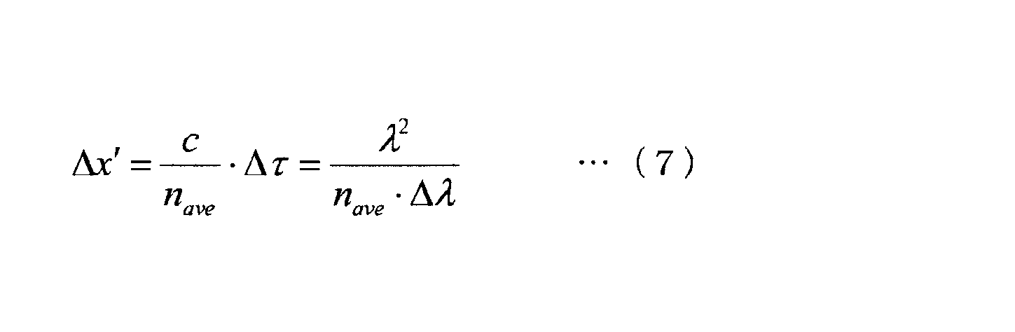
- ⁇ x ′ 2 ⁇ x is set in consideration of the round-trip distance.
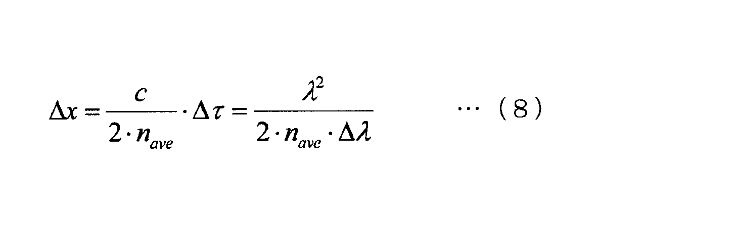
- the data interval ⁇ x of the reflected light spectrum after the FFT is as follows.
- the maximum measured optical thickness x max can be expressed by the following equation.
- ⁇ can be considered as the minimum period of FFT, and therefore, ⁇ can be considered as the measurement wavelength range or wavelength scan range of the spectrometer. Assuming that the wavelength span (measurement wavelength region) is ⁇ w and the center wavelength of the spectrometer is ⁇ 0 , Expressions 12 and 13 are expressed by the following expressions.
- the thickness of the measurement object is examined using a specific example.
- the maximum measured optical thickness X max is 15 from Equation 12. 4 mm.
- the sampling number N s is a fixed value for the number of sequences, it is not easy to change.
- the sampling number N s of the wavelength axis direction can be set in any way. For example in the case of setting the number of samplings N s 5000, etc., it can measure the thick measurement target of about 10 times that of the 512 CCD array which is arranged.
- the wavelength range ⁇ w of the spectroscope is widened according to Equation 12, the data interval ⁇ X after FFT can be reduced. Accordingly, it can be seen that reducing the data interval and increasing the measurable thickness are not compatible.
- the above is a general formula that does not depend on the refractive index. Therefore, when converting to a real scale in a medium having a refractive index n ave , each may be divided by 2n ave .
- FIG. 10 is a schematic diagram for explaining the minimum spatial resolution.
- “B” in FIG. 10 is a spectrum showing an intensity distribution depending on the wave number k of the light source that can be approximated by a Gaussian function.
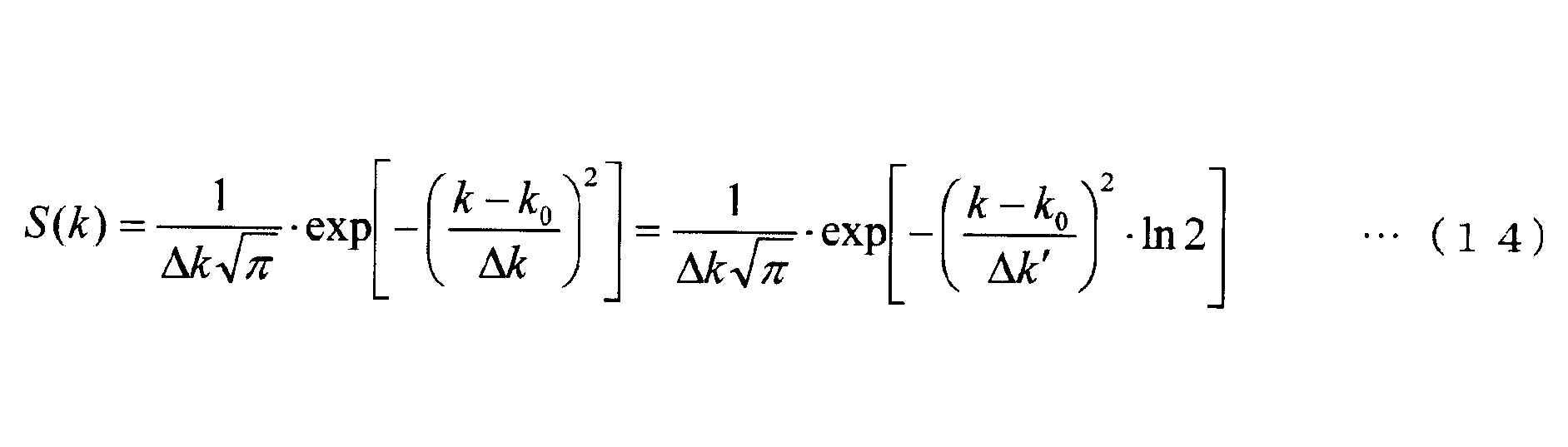
- the intensity S (k) of the spectrum shown in “b” of FIG. 10 is given by the following formula, where the wave number of the peak value is k0, the intensity of the peak value is 1 / ⁇ k ⁇ ( ⁇ ) 1/2, and the half width at half maximum is ⁇ k.
- the wave number of the peak value is k0
- the intensity of the peak value is 1 / ⁇ k ⁇ ( ⁇ ) 1/2
- the half width at half maximum is ⁇ k.
- the relationship is established.
- the half-value half width ⁇ k can be expressed as follows using Equations 15 and 16.
- the half-value half width l c of the spectrum of intensity S (x) is the coherence length.
- Minimum resolution space is l c, it is determined by the center wavelength and the half value width of the spectrum of the light source 10.
- a necessary sampling number N s condition is derived based on the above-described maximum measurement optical thickness x max .
- the center wavelength of the light source 10 is ⁇ 0
- the half width of the light source spectrum is ⁇
- the wavelength span that is the wavelength sweep range of the tunable filter 40 is ⁇ w
- the refractive index of the dielectric layer 120 is n
- the maximum measured optical thickness x max is expressed by the following formula.
- the maximum measured thickness d and the maximum measured optical thickness x max must satisfy the following conditions.
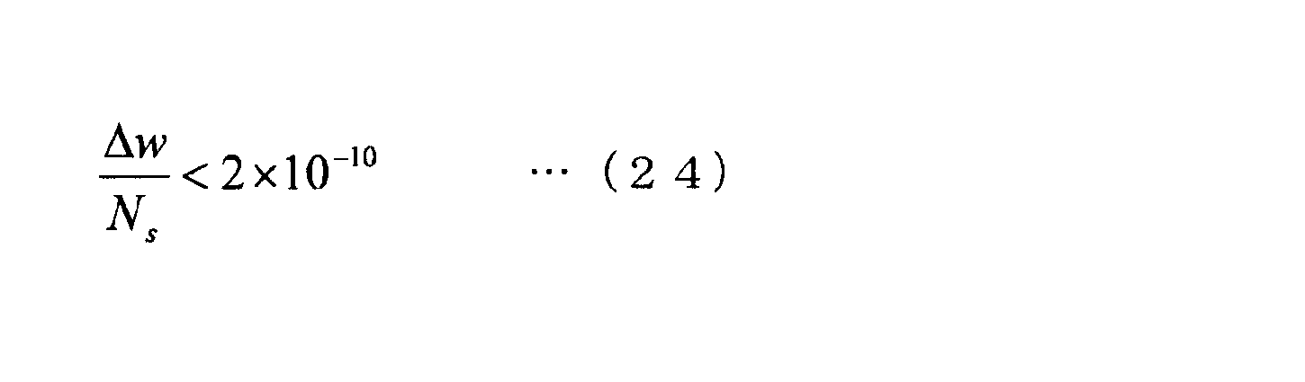
- wavelength span ⁇ w [m] is converted into ⁇ w ′ [nm] and expressed as follows.
- the interference optical system 1 performs sampling at a sampling number N s with sweeping in wavelength span ⁇ w '[nm] which satisfies the relationship shown in equation 25. For example, when the wavelength span ⁇ w '[nm] is 40nm performs sampling as sampling number N s is 200 greater than.
- the spatial resolution in the thickness direction of the measurement object will be examined.
- the coherence length is 0.7 ⁇ m using Equation 20. Since the coherence length is the half width at half maximum of the Gaussian function, the spatial resolution can be doubled to about 1.4 ⁇ m.
- the frequency domain method when an SC light source is used, the data interval ⁇ x after FFT is 3.2 ⁇ m using Equation 13.
- the weighted centroid of the 2nd signal having a certain width is calculated in order to accurately obtain the 2nd position after the FFT. Then, a change in the optical path length 2nd is detected based on a change in the position of the weighted center of gravity.
- the weighted center of gravity in order to determine the weighted center of gravity with high accuracy close to the 2nd signal shape Gaussian function after FFT, and, at least three of the plurality of sampling points are required for full width at half maximum within 2l c.
- the 2nd signal shape In order for the 2nd signal shape to be a Gaussian function, the light source spectrum itself must also be a Gaussian function.
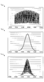
- the reflected light spectrum shown in “a” in FIG. 11 is an example of a spectrum close to a Gaussian function.
- “B” in FIG. 11 is a signal after FFT of the reflected light spectrum shown in “a” in FIG.
- the signal shape after FFT is close to a Gaussian function, and the skirt portion is sufficiently included in the detection range 1540 to 1580 nm, so that the position of the center of gravity can be obtained appropriately.
- the bottom part protrudes greatly from the detection range as in the reflected light spectrum shown in “a” of FIG.
- the peak becomes sharp as shown in the signal of “b” in FIG.
- the accuracy of is reduced.
- the center wavelength of the detection range is different from the center wavelength of the reflected light spectrum as in the reflected light spectrum shown in “a” in FIG. 13
- the shape is a Gaussian function as in the signal shown in “b” in FIG.
- the accuracy of the center of gravity is reduced.
- a Gaussian function is used as the window function.
- a Gaussian function there are one that normalizes the area to 1 and one that normalizes the height to 1.
- “A” in FIG. 14 is an example of a Gaussian function that normalizes the area to 1. Assuming that the center wavelength is ⁇ 0 and the half width at half maximum is ⁇ HWHM , the Gaussian function shown in “a” of FIG. 14 is expressed as follows.
- “b” in FIG. 14 is an example of a Gaussian function that normalizes the height to 1.
- the Gaussian function shown in “b” of FIG. 14 is expressed as follows.
- the edge of the measurement region is attenuated by about 97%, it can be said that the shape of the 2nd signal after the FFT is close to a Gaussian function.
- the window function measurement can be performed without worrying about the wavelength of the light source, the spectral width, the center wavelength of the measuring system such as a spectroscope, the band, and the like.
- C in FIG. 15 is a signal obtained by applying the Gaussian function shown in “b” of FIG. 15 to the reflected light spectrum shown in “a” of FIG.
- the center wavelength ⁇ 0 1548 nm
- the half width at half maximum ⁇ HWHM 30 nm
- the sample thickness d 775 ⁇ m
- the refractive index n of the sample is 3.7.
- the 2nd signal after FFT is as shown in “b” of FIG. “C” in FIG. 16 is an enlarged view of the peak portion of “b” in FIG.
- FIG. 18 is a graph showing the relationship between the half-value half width ⁇ HWHM of the light source and the waveform width after FFT.
- the width of the 2nd waveform after the FFT changes. The more points that make up the peak shape after FFT, the more accurate the calculation of the center of gravity. That is, the width of the 2nd waveform after FFT can be increased as the half-value half width ⁇ HWHM of the light source is reduced.
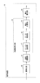
- FIG. 19 is a flowchart showing the operation of the optical interference system 1.
- the control process shown in FIG. 19 is repeatedly executed at a predetermined interval from the timing when the power source of the light source 10 and the arithmetic device 15 is turned on, for example. It is assumed that the tunable filter 40 has been set in advance before the execution of FIG. That is, it is assumed that the relationship between the applied voltage (or applied frequency) and the wavelength of transmitted light is acquired in advance, for example, as shown in FIG.
- the light source 10 generates measurement light.
- the light receiving element 41 acquires the spectrum of the reflected light reflected by the front surface 120a and the back surface 120b of the dielectric layer 120. That is, the light receiving element 41 detects the wavelength while sweeping the wavelength by the tunable filter 40. Thereby, for example, the reflected light of the spectrum shown in “b” of FIG. 20 is obtained.
- the optical path length calculation unit 16 inputs the spectrum of reflected light from the light receiving element 41.
- the process of S10 ends, the process proceeds to a waveform adjustment process (S11).
- the waveform adjustment unit 31 adjusts the waveform. That is, the window function described above is applied to the reflected light spectrum.
- the process of S11 ends, the process proceeds to a coordinate conversion process (S12).
- the optical path length calculation unit 16 converts the coordinate axis of the spectrum obtained in the process of S11 from the wavelength ⁇ to the spatial frequency (1 / ⁇ ). For example, the spectrum shown in “c” of FIG.
- the process proceeds to the first data interpolation process (S14).
- the optical path length calculation unit 16 performs data interpolation of the spectrum obtained in the process of S12.
- the sampling number is N s
- the spectrum data is (x 0 , x 1 , x 2 ,..., X Ns-1 )
- the intensity array is (y 0 , y 1 , y 2 ,..., Y Ns-1 ).
- the optical path length calculation unit 16 rearranges the spatial frequency array at equal intervals. For example, assuming that the spatial frequency included in the rearranged spatial frequency array is X i , rearrangement is performed using the following equation.
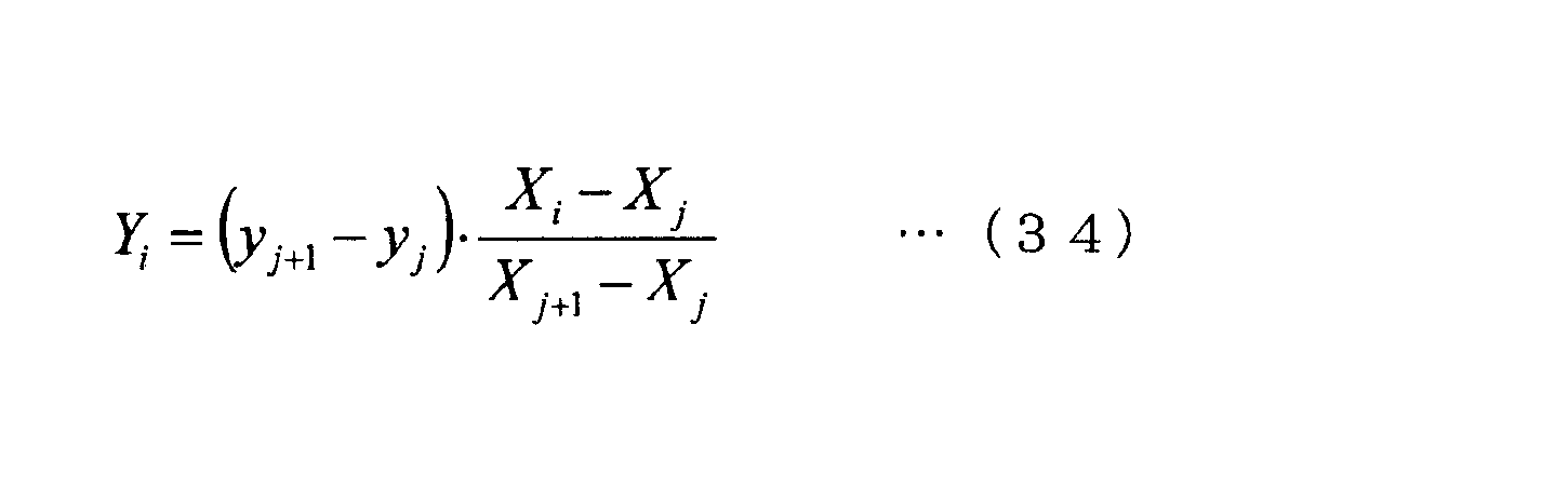
- the optical path length calculation unit 16 calculates the intensity at the spatial frequency X i after the rearrangement by linear interpolation. If the intensity at this time is Y i , it is calculated using the following equation.
- the Fourier transform unit 17 Fourier transforms the spectrum interpolated in the process of S14 (Fourier transform process). Thereby, for example, as shown in “b” of FIG. 21, the vertical axis is the amplitude and the horizontal axis is the phase spectrum.
- the process of S16 ends, the process proceeds to a filtering process (S18).
- S20 an extraction process
- the process of S20 ends, the process proceeds to the second data interpolation process (S22).
- the data interpolation unit 18 interpolates the 2nd peak data obtained in the process of S20 (data interpolation process).
- Interpolation number N A is set in advance based on, for example, the required precision.
- data interpolation is performed using the following formula.
- j is an index used for the intensity array.
- the process of S22 ends, the process proceeds to the extraction process (S24).
- the centroid calculator 19 extracts only the data range used for the calculation of the centroid from the data interpolated in the process of S22.
- the center-of-gravity calculation unit 19 sets A to be a threshold used for the center-of-gravity calculation, and substitutes 0 for intensity data Y equal to or less than the maximum intensity Y MAX ⁇ A of the peak.
- the centroid calculating unit 19 calculates a weighted centroid from the data interpolated in the process of S24 (weighted centroid calculating step). For example, the following formula is used.
- N is the number of data points after extracting the center of gravity range.
- the thickness calculation unit 20 divides the optical path length nd obtained in the process of S26 by the refractive index of the material of the measurement object (here, the dielectric layer 120), thereby obtaining the thickness of the measurement object. Is calculated (thickness calculation step).
- the control process shown in FIG. 19 ends.
- the measurement accuracy of the thickness of the dielectric layer 120 by the measurement method of the present embodiment is in the range of ⁇ 6 ⁇ m to +6 ⁇ m, which is 3% or less of the allowable range of the thickness variation of the dielectric layer 120. You can see that it is obtained.
- the waveform before the Fourier transform can be converted into a waveform suitable for the Fourier transform by using the window function. It is possible to have a width of. Therefore, the peak position detection accuracy can be improved.
- the interpolation method described above is not limited to linear interpolation, and may be polynomial interpolation.
- the surface 120c1 in the dot 120c is a mirror surface, and the surface 120d outside the dot 120c is left as a sand surface by sandblasting.
- “a” in FIG. 22 shows the thickness d from the surface 120 c 1 of the dot 120 c to the bottom surface of the dielectric layer 120.
- a distance of 200 mm from the collimator 12 to the surface 120c1 of the dot 120c is shown.
- the distance from the collimator 12 to the surface 120c1 of the dot 120c is not limited to this.
- the collimator 12 is horizontally moved by using an adjustment mechanism 12 a capable of horizontally moving the collimator 12, and light is applied from the surface 120 c 1 of the dot 120 c to the dielectric layer 120.
- the adjustment mechanism 12a can adjust the angle of the collimator 12 along with the horizontal movement. Thereby, the incident angle of the measurement light output from the collimator 12 to the dielectric layer 120 can be adjusted.
- the surface 120a of the dielectric layer 120 is flattened by polishing.
- the electrode layer 110 (dielectric material) is deformed from the surface 120a of the dielectric layer 12.
- the distance to the back surface 120b) of the layer 12 is not uniform.
- the intensity of the reflected light is generally maximized when it is perpendicularly incident on the electrostatic chuck 100, but the signal after the FFT processing of S16 in FIG. 19 is not necessarily maximized.
- window functions such as a rectangular window, a Gaussian window, and a Hamming window are used.
- a window function here, a rectangular window
- the waveform outside the finite section is recognized as 0, and the waveform shape at the end of the finite section becomes distorted.
- the resolution of the peak of the signal intensity after FFT processing is a trade-off between the resolution of the peak of the signal intensity after FFT processing and the dynamic range.
- the collimator 12 is moved horizontally by the adjustment mechanism 12a, light is incident from one point in the dot 120c formed on the dielectric layer 120, and the dielectric layer thickness measuring method according to the present embodiment is used.
- the thickness of the dielectric layer 120 was measured.
- the horizontal axis represents the measurement time (seconds)
- the vertical axis represents the thickness d ( ⁇ m) of the dielectric layer 120 obtained as a result of the measurement. According to this result, the average of the thickness d was 385.97 ⁇ m, and the measurement accuracy in the steady state was ⁇ 0.787 ⁇ m.
- the thickness of the dielectric layer must be not less than “the lower limit thickness at which the dielectric layer causes dielectric breakdown” and not more than “the upper limit thickness at which the substrate can be attracted by the electrostatic chuck”. . That is, high design accuracy is required for the thickness of the dielectric layer.
- the numerical value from the surface 110a of the electrode layer 110 to the surface 120a of the dielectric layer 120 is about several hundred ⁇ m. More desirably, it is about 200 ⁇ m or more and 400 ⁇ m or less. Therefore, the allowable range of the strain ⁇ of the electrode layer 110 shown in STEP 3 of FIG. 1 needs to be measured with a resolution of ⁇ m order. As described above, a method for measuring the thickness of the dielectric layer is required to have a high resolution.
- the arithmetic unit 15 determines whether the measured thickness of the dielectric layer 120 is 200 ⁇ m or more and 400 ⁇ m or less, and when the thickness is smaller than 200 ⁇ m or larger than 400 ⁇ m. May display a warning.
- the present invention is not limited to this, and the arithmetic unit 15 may determine whether the measured thickness of the dielectric layer 120 is within a predetermined range.
- the predetermined range may be a range of about several hundred ⁇ m. As a result of the determination, when the measured thickness of the dielectric layer 120 is not included in the predetermined range, a warning may be displayed.
- the arithmetic unit 15 determines whether the difference between the maximum value (Max) and the minimum value (Min) of the thickness of the dielectric layer 120 is 200 ⁇ m or less. A warning may be displayed.
- the present invention is not limited to this, and the computing device 15 may determine whether the difference between the measured maximum value and minimum value of the dielectric layer 120 is equal to or less than a predetermined threshold value.
- the predetermined threshold may be a value of about several hundred ⁇ m.
- a warning may be displayed when the difference between the maximum value and the minimum value of the measured thickness of the dielectric layer 120 is not more than a predetermined threshold value.
- the measurement object can be measured with high accuracy on the order of ⁇ m even for the method for measuring the thickness of the dielectric layer according to the present embodiment.
- the measurement accuracy of the thickness d of the dielectric layer 120 in the steady state shown in FIG. 23 is ⁇ 0.787 ⁇ m, and the accuracy is ⁇ 1 ⁇ m or less. This indicates that the method for measuring the thickness of the dielectric layer according to the present embodiment has sufficient accuracy for measuring the thickness of the dielectric layer.
- the collimator 12 was finely adjusted in the horizontal direction by the adjusting mechanism 12a, and the thickness of the dielectric layer 120 when light was incident from a plurality of points within the same dot 120c was measured.
- the result is shown in FIG.
- the horizontal axis represents the measurement time (seconds), and the vertical axis represents the thickness d ( ⁇ m) of the dielectric layer 120 obtained as a result of the measurement.
- the thickness d fluctuated by about 11 ⁇ m between the minimum value (Min) and the maximum value (Max). Therefore, the measurement accuracy of the thickness d of the dielectric layer 120 when the measurement position is moved within the same dot is ⁇ 5.5 ⁇ m.
- the method for measuring the thickness of the dielectric layer according to the present embodiment has sufficient accuracy for measuring the thickness of the dielectric layer having a dot shape on the surface.
- the planarity in one dot 120c can be measured. Thereby, the attraction force due to the contact area between the electrostatic chuck 100 and the wafer can be predicted.
- the collimator 12 was used.
- the collimator 12 emits measurement light adjusted as parallel rays to the dielectric layer 120. Therefore, the collimator 12 is useful when the distance to the measurement object is long.
- the focuser 13 collects the measurement light and emits it to the dielectric layer 120. Therefore, the focuser 13 is useful when the distance to the measurement object is fixed.
- “a” in FIG. 25 shows an example in which a focuser 13 having a focal length of 200 mm and a beam diameter of 1 mm is used and the spot diameter is 100 ⁇ m.
- the allowable distortion of the surface of the dot 120 is approximately 0.3 degrees when the electrostatic chuck 100 is horizontal.
- the focuser 13 it is possible to measure the pinpoint thickness even for a measurement object having an uneven surface. That is, according to the method for measuring the thickness of the dielectric layer according to the present embodiment, by using the focuser 13, the thickness of the dielectric layer 120 can be accurately increased even in the electrostatic chuck 100 having a dot shape on the surface. It can be measured.
- the dot diameter shown in “a” in FIG. 25 is about 2 mm, but as shown in “c” in FIG. 25, the dot diameter may be about several hundred ⁇ m in the future. There is. As described above, if the focuser 13 is used, the measurement light can be incident on the minute dots 120c, and thus pinpoint thickness measurement is possible.
- the dielectric layer 120 has a cylindrical shape, and the surface of the dielectric layer 120 is circular as shown in “a” of FIG. A plurality of dots 120 c are regularly formed on the surface of the dielectric layer 120.
- the occurrence position of abnormal discharge is shown on the outermost periphery on the upper right side (Y axis -60 °) of the dielectric layer 120.
- “B” in FIG. 26 indicates a measurement position in the present embodiment.
- the measurement position is the axis of line A going to the Y axis + 0 ° with the notch position of ⁇ 180 ° as the Y axis, the axis of line B rotated by ⁇ 120 ° with respect to line A, and rotated by ⁇ 60 ° with respect to line A.
- the axis of the line C Measuring light is incident on the dots 120c located on each line.
- the dot 120c located on each line (that is, in the diametrical direction) intersects the center position O of the dielectric layer 120 and the circumferences of the radius 50 mm, the radius 100 mm, and the radius 145.5 mm from the center position O. In the position. Therefore, there are seven measurement positions on the dot 120c of each line.
- the horizontal axis indicates the center position O
- the vertical axis indicates the thickness of the dielectric layer 120 at each measurement position.
- the measurement result is shown.
- the thickness of the dielectric layer 120 is approximately 300 ⁇ m to 470 ⁇ m
- the variation in the thickness of the dielectric layer 120 is within 200 ⁇ m which is an allowable range of distortion of the electrode layer 110.
- the thickness of the dielectric layer 120 was the thinnest at about 240 ⁇ m at the dot position 120c2 in the vicinity of the abnormal discharge occurrence position.
- the measurement result of the dot 120c positioned in each circumferential direction from the center position O to the radius 50 mm, the radius 100 mm, and the radius 145.5 mm is shown in “b” of FIG.
- the thickness of the dielectric layer 120 was measured at a plurality of dot positions located in the circumferential direction around the notch position (180 °). The number of measurement positions (dot positions) increases toward the outer peripheral side.
- the variation in the thickness of the dielectric layer 120 is small in the circumferential direction with a radius of 50 mm and a radius of 100 mm, and large at the outermost periphery with a radius of 145.5 mm. That is, the strain of the electrode layer 110 on the outermost periphery (radius 145.5 mm) of the dielectric layer 120 is larger than the strain of the electrode layer 110 located on the inner peripheral side. Particularly, at the position where the abnormal discharge occurs, the distortion of the electrode layer 110 is the largest and the thickness of the dielectric layer 120 is the smallest. From the results of “a” in FIG. 27 and “b” in FIG. 27 described above, the occurrence position of the abnormal discharge coincided with the measurement position where the thickness of the dielectric layer 120 was the thinnest.
- the thickness of the dielectric layer 120 was measured by polishing the surface of the dielectric layer 120. As a result, the validity of the numerical value by the dielectric layer thickness measurement method according to the present embodiment was confirmed. From the above, it was proved that according to the method for measuring the thickness of the dielectric layer according to the present embodiment, the measurement object can be measured with high accuracy and in a non-contact manner.
- optical interference system and the method for measuring the thickness of the dielectric layer have been described above.
- the optical interference system and the method for measuring the thickness of the dielectric layer according to the present invention are limited to the above embodiment.
- various modifications and improvements are possible within the scope of the present invention.
- the light source spectrum may be acquired and recorded in advance before the execution of the control process shown in FIG. 19, and the reflected light spectrum may be normalized by the normalization unit 30 before the adjustment process shown in S11.
- the light source spectrum shown in “a” in FIG. 28 is acquired in advance.
- the reflected light spectrum of the Si substrate shown in “b” of FIG. 28 is acquired.
- the normalization unit 30 normalizes the reflected light spectrum using the light source spectrum.
- the reflected light spectrum is divided by the light source spectrum to obtain the reflectance.
- “A” in FIG. 29 is an example of a spectrum normalized to reflectivity.
- the tunable filter 40 shown in FIG. 2 may be provided between the light source 10 and the optical circulator 11 or may be provided between the optical circulator 11 and the collimator 12.
- a movable grating spectroscope may be used.
- the spectroscope 14a includes a movable grading spectrum meter and a single light receiving element, and the arithmetic unit 15 and the spectrum meter cooperate to control the wavelength ⁇ of transmitted light.
- an optical spectrum analyzer may be used as a movable grading spectroscope.
- the arithmetic unit 15 may control the wavelength of the light source 10.
- the wavelength of the light source 10 is changed depending on the material of the measurement object.
- the wavelength sweeping section may be anything.
- the light source any light can be used as long as the interference between the measurement light and the reference light can be measured.
- the light from the light source is preferably light that does not cause interference with reflected light from at least the distance between the front surface and the back surface of the measurement object (usually about 800 to 1500 ⁇ m).
- low coherence light refers to light with a short coherence length.
- the center wavelength of the low coherence light is preferably 0.3 to 20 ⁇ m, for example, and more preferably 0.5 to 5 ⁇ m.
- the coherence length is preferably, for example, 0.1 to 100 ⁇ m, and more preferably 3 ⁇ m or less.
- an SLD Super Luminescent Diode
- LED high-intensity lamp (tungsten lamp, xenon lamp, etc.), ultra-wideband wavelength light source, or the like
- a high-luminance SLD wavelength, for example, 1300 nm
- the thickness of the wafer, the focus ring and the counter electrode can be measured by mounting the optical interference system 1 according to the present invention on the substrate processing apparatus.
- these parts need to be formed of a material that is transparent to the measurement light. is there.
- silicon, quartz, sapphire, or the like is used as the material for the chamber parts.
- SYMBOLS 1 Optical interference system, 10 ... Light source, 11 ... Optical circulator, 12 ... Collimator, 13 ... Focuser, 15 ... Arithmetic unit, 16 ... Optical path length calculation part, 17 ... Fourier transform part, 18 ... Data interpolation part, 19 ... Gravity center Calculation unit, 20 ... thickness calculation unit, 30 ... standardization unit, 31 ... waveform adjustment unit, 40 ... tunable filter, 41 ... light receiving element, 42 ... A / D conversion unit, 43 ... wavelength control unit, 100 ... static Electric chuck, 110 ... electrode layer, 120, 130 ... dielectric layer
Landscapes
- Physics & Mathematics (AREA)
- General Physics & Mathematics (AREA)
- Health & Medical Sciences (AREA)
- General Health & Medical Sciences (AREA)
- Nuclear Medicine, Radiotherapy & Molecular Imaging (AREA)
- Radiology & Medical Imaging (AREA)
- Length Measuring Devices By Optical Means (AREA)
Abstract
光源から測定対象物を透過する波長を有する測定光を出力し、コリメータ又はフォーカサーを移動させて、前記コリメータ等から前記出力した測定光を前記測定対象物の第1主面の計測位置へ出射し、前記第1主面及び対向する第2主面からの反射光を前記コリメータ等へ入射し、前記コリメータ等からの反射光を受光素子に入射し、前記受光素子に入射された光の強度を取得し、前記受光素子に入射された光の波長を掃引し、前記取得した光の強度及び前記掃引した光の波長を用いて、波長に依存した強度分布であって前記第1主面及び前記第2主面からの反射光の強度分布である干渉強度分布を測定し、前記干渉強度分布をフーリエ変換して得られる波形に基づいて前記測定対象物の厚さを前記測定対象物に非接触に計測する、ことを含む計測方法が提供される。
Description
測定対象物の厚さ計測方法に関する。
基板処理装置の内部には様々な装置が設けられている。例えば、基板は、載置台に設けられた静電チャック(ESC:Electrostatic Chuck)上に載置される。静電チャックは、導電性のシート状の電極層の表裏を誘電体層にて挟んだ構成を有する(例えば、特許文献1を参照)。基板は、直流電圧源から電極層に電圧を印加することにより生じるクーロン力によって静電チャックに吸着される。
通常、静電チャックの製造例としては、図1のSTEP1に示したように、電極層110の表裏を誘電体層120、130によって挟んで積層させた状態で焼結させる方法が用いられることが多い。誘電体層120、130にセラミックを用いる場合、焼結する際、図1のSTEP2に示したように、静電チャック100は、圧力がかけられた状態で高温処理される。このため、圧力や熱応力等により静電チャック100に歪みが生じることがある。焼結後、図1のSTEP3に示したように、静電チャック100の表裏面は、研磨され平坦化される。
しかしながら、静電チャック100の表裏面が平坦化されても、例えば、図1のSTEP3に示したように焼結時に静電チャック100の内部が歪んだ状態では、誘電体層120、130の厚さは不均一になる。
一方、誘電体層120、130の厚さには高い均一性が要求される。例えば、誘電体層120、130の厚さが設計値よりも厚い場合、熱容量が大きくなるために熱応答性が悪くなり、基板の温度制御性が悪化する。また、静電力が弱くなるために基板に対して十分な吸着力が得られず、特に基板の裏面に供給する伝熱ガスの圧力が高い場合等に基板が静電チャック100から跳ねる要因となる。
また、例えば、誘電体層120、130の厚さが設計値よりも薄い場合、静電チャック100に十分な機械的強度が得られない。また、絶縁性が十分でないために絶縁破壊を生じさせ、リーク電流や異常放電を発生させることがある。
以上のように、基板処理装置に取り付けられる静電チャック等の装置には、高い設計精度が求められる。よって、製造された装置の中から高い性能を有する装置を選別するためには、高精度で装置内の状態を計測する方法が望まれる。また、パーティクルや汚染防止対策の観点から非接触で装置内の状態を計測できることが好ましい。
上記課題に対して、一側面では、測定対象物の厚みを非接触で精度良く計測することを目的とする。
上記課題を解決するために、一の態様によれば、
第1主面及び前記第1主面に対向する第2主面を有する測定対象物の厚さを計測する方法であって、
光源から前記測定対象物を透過する波長を有する測定光を出力する第1のステップと、
コリメータ又はフォーカサーを移動させて、前記コリメータ又はフォーカサーから前記出力した測定光を前記測定対象物の第1主面の計測位置へ出射し、前記第1主面及び前記第2主面からの反射光を前記コリメータ又はフォーカサーへ入射する第2のステップと、
前記コリメータ又はフォーカサーからの反射光を受光素子に入射し、前記受光素子に入射された光の強度を取得し、前記受光素子に入射された光の波長を掃引する第3のステップと、
前記取得した光の強度及び前記掃引した光の波長を用いて、波長に依存した強度分布であって前記第1主面及び前記第2主面からの反射光の強度分布である干渉強度分布を測定する第4のステップと、
前記干渉強度分布をフーリエ変換して得られる波形に基づいて前記測定対象物の厚さを前記測定対象物に非接触に計測する第5のステップと、
を含むことを特徴とする計測方法が提供される。
第1主面及び前記第1主面に対向する第2主面を有する測定対象物の厚さを計測する方法であって、
光源から前記測定対象物を透過する波長を有する測定光を出力する第1のステップと、
コリメータ又はフォーカサーを移動させて、前記コリメータ又はフォーカサーから前記出力した測定光を前記測定対象物の第1主面の計測位置へ出射し、前記第1主面及び前記第2主面からの反射光を前記コリメータ又はフォーカサーへ入射する第2のステップと、
前記コリメータ又はフォーカサーからの反射光を受光素子に入射し、前記受光素子に入射された光の強度を取得し、前記受光素子に入射された光の波長を掃引する第3のステップと、
前記取得した光の強度及び前記掃引した光の波長を用いて、波長に依存した強度分布であって前記第1主面及び前記第2主面からの反射光の強度分布である干渉強度分布を測定する第4のステップと、
前記干渉強度分布をフーリエ変換して得られる波形に基づいて前記測定対象物の厚さを前記測定対象物に非接触に計測する第5のステップと、
を含むことを特徴とする計測方法が提供される。
一の態様によれば、測定対象物の厚みを非接触で精度良く計測することができる。
以下、本発明を実施するための形態について図面を参照して説明する。なお、本明細書及び図面において、実質的に同一の構成については、同一の符号を付することにより重複した説明を省く。
[静電チャックの内部の計測]
図1に示した静電チャック100の誘電体層120、130の厚さには高い均一性が要求される。例えば、誘電体層120、130の厚さが設計値よりも厚い場合、熱容量が大きくなるために熱応答性が悪くなり、基板の温度制御性が悪化する。また、静電力が弱くなるために基板に対して十分な吸着力が得られず、特に基板の裏面に供給する伝熱ガスの圧力が高い場合等に基板が静電チャック100から跳ねることがある。
図1に示した静電チャック100の誘電体層120、130の厚さには高い均一性が要求される。例えば、誘電体層120、130の厚さが設計値よりも厚い場合、熱容量が大きくなるために熱応答性が悪くなり、基板の温度制御性が悪化する。また、静電力が弱くなるために基板に対して十分な吸着力が得られず、特に基板の裏面に供給する伝熱ガスの圧力が高い場合等に基板が静電チャック100から跳ねることがある。
また、例えば、誘電体層120、130の厚さが設計値よりも薄い場合、静電チャック100に十分な機械的強度が得られない。また、絶縁性が十分でないために絶縁破壊を生じさせ、リーク電流や異常放電を発生させることがある。
このように、誘電体層120、130の厚さの均一性は、静電チャック100の性能の良し悪しに繋がる。しかしながら、静電チャック100の製造工程では、焼結時に静電チャック100にかかる圧力や熱応力等によって内部に歪みが生じる場合がある(図1のSTEP2)。歪みがある状態で誘電体層120,130の表面120a,130aを研磨すると、誘電体層120、130の表面120a、130aは平坦になる。しかし、静電チャック100の内部の歪みにより、誘電体層120、130の厚さは不均一になる(図1のSTEP3)。
誘電体層120、130の厚さが均一で、高い性能を有する静電チャック100を選別するためには、誘電体層120の表面120aから電極層110の表面110aまでの距離を高精度かつ非破壊で計測する方法が望まれる。また、誘電体層の厚さを計測する際、パーティクルや汚染防止対策の観点から非接触で計測されることが好ましい。
誘電体層の厚さを計測する方法の一例としては、静電容量の計測値から計算する方法がある。しかし、この方法では、誘電体層の表面に計測用のプローブが接触するため、パーティクルや金属汚染が発生する場合がある。これに対して、パーティクルや金属汚染の対策としてプローブにキャップを付けて計測する方法がある。しかし、この場合、プローブの押し付け圧力によって計測された数値に誤差が生じてしまう可能性がある。また、静電チャック100は積層構造であり、製造時に研磨による平坦化処理(図1のSTEP3参照)が行われるため、静電チャック100の全体の厚さを計測しただけでは、静電チャック100の内部に生じている歪みを計測することはできない。
また、誘電体層の厚みについては、前述のように高い設計精度が要求されている。つまり、「誘電体層が絶縁破壊を発生する下限の厚み」以上であって、「静電チャックによって基板を吸着可能な上限の厚み」以下でなければならない。一般的な静電チャックの場合、電極層110の表面110aから誘電体層120の表面120aまでの数値は数百μm程度である。より望ましくは、約200μm以上400μm以下である。したがって、図1のSTEP3に示した電極層110の歪みαの許容範囲もμmオーダーの分解能で測定する必要がある。このように、誘電体層の厚さを計測する方法には高精度な分解能が要求され、静電容量の計測値から誘電体層の厚さを計算する方法では困難である。
これに対して、本実施形態では、誘電体層の厚さを光学的に計測する方法を提案する。これにより、誘電体層を高精度かつ非接触に計測することができる。以下、本実施形態に係る誘電体層の厚さを計測する方法について説明する。
[システムの全体構成]
まず、本実施形態に係る光干渉システムについて、図2を参照しながら説明する。図2は、一実施形態に係る光干渉システムの全体構成図である。
まず、本実施形態に係る光干渉システムについて、図2を参照しながら説明する。図2は、一実施形態に係る光干渉システムの全体構成図である。
光干渉システム1は、一実施形態に係る誘電体層の厚さの計測方法を実行するシステムである。光干渉システム1は、OCT(Optical Coherence Tomography)を利用して測定対象物の厚さを計測する。
光干渉システム1は、光源10、光サーキュレータ11、コリメータ12、チューナブルフィルタ40、受光素子41、A/D変換部42、波長制御部43及び演算装置15を有している。なお、光源10、光サーキュレータ11、コリメータ12、チューナブルフィルタ40及び受光素子41のそれぞれは、光ファイバーケーブルにより接続されている。
光源10は、本実施形態の測定対象物である誘電体層120を透過する波長の測定光を出力する。光源10として、例えばSLD(Super Luminescent Diode)が用いられる。誘電体層120は、例えば板状を呈し、表面120a及び裏面120bを有している。
裏面120bは、電極層110との接触面である。本実施形態では、測定対象物の一例として、静電チャック100に使用される誘電体層の厚さを計測する。測定対象物の他の例としては、SiO2(石英)又はAl2O3(サファイア)等の誘電体の他、例えばSi(シリコン)が挙げられる。誘電体層120の表面120aは、測定対象物の第1主面の一例であり、誘電体層120の裏面120bは、測定対象物の第1主面に対向する第2主面の一例である。
光サーキュレータ11は、光源10、コリメータ12及びチューナブルフィルタ40に接続されている。光サーキュレータ11は、光源10で発生した測定光をコリメータ12へ出射する。光サーキュレータ11に替えて、2×1又は2×2のフォトカプラを用いてもよい。
コリメータ12は、平行光線として調整された測定光を誘電体層120へ出射する。測定光は、誘電体層120の表面120aから誘電体層を透過し、誘電体層120の裏面120b(電極層との接触面)で反射する。コリメータ12は、誘電体層120からの反射光を入射する。反射光には、表面120aの反射光だけでなく裏面120bの反射光が含まれる。コリメータ12は、反射光を光サーキュレータ11へ出射する。光サーキュレータ11は、反射光をチューナブルフィルタ40へ出射する。なお、コリメータ12に替えてフォーカサーを使用してもよい。フォーカサーを使用した方が好ましい場合については後述する。
チューナブルフィルタ40は、入力光の波長を変更可能な波長可変フィルタである。チューナブルフィルタ40は、ファブリペロー方式、回折格子方式、干渉フィルタ方式、音響光学方式等、印加電圧や印加周波数を制御することによりフィルタを透過させた透過光の波長を制御できるものであれば何でもよい。印加電圧や印加周波数は後述する波長制御部43により制御される。チューナブルフィルタ40は、透過光を受光素子41へ出射する。
受光素子41は、光を検出する素子であり、例えば光の強度に応じた信号を出力する。ここでは単一の受光素子41が用いられる。受光素子41として、例えばフォトダイオードや光電子増倍管が用いられる。受光素子41は出力信号をA/D変換部42へ出力する。
A/D変換部42は、受光素子41のアナログ出力信号をデジタル信号に変換する。A/D変換タイミングは波長制御部43により制御される。A/D変換部42は、デジタル信号を演算装置15へ出力する。演算装置15は、PC等の機器で実現される制御部の一例である。
波長制御部43は、チューナブルフィルタ40に接続され、チューナブルフィルタ40への印加電圧を制御する。また、波長制御部43は、A/D変換部42に接続され、印加電圧の制御タイミングとA/D変換タイミングとの同期をとる。
チューナブルフィルタ40、受光素子41、A/D変換部42及び波長制御部43によって、反射光の反射光スペクトル(干渉強度分布)が測定される。反射光スペクトルは、反射光の波長又は周波数に依存した強度分布を示す。A/D変換部42から演算装置15へ出力されるデジタル信号は、反射光スペクトルとなる。
演算装置15は、反射光スペクトルに基づいて誘電体層120の厚さを計測する。図3は、演算装置15の機能ブロック図である。図3に示すように、演算装置15は、規格化部30、波形調整部31、光路長算出部16及び厚さ算出部20を備えている。
規格化部30は、反射光スペクトルの波形を、予め取得された光源10の測定光のスペクトルを用いて規格化する。例えば、光源10の光源スペクトル(測定光のスペクトル)のプロファイルが歪んでいる場合や非対称である場合には、後述する処理後の信号も歪んでしまい、結果として精度の高い測定をすることができないおそれがある。このため、反射光スペクトルを光源スペクトルで除算して規格化する。すなわち、反射率の波形とする。規格化部30は、算出した波形を波形調整部31へ出力する。
波形調整部31は、波長に依存した窓関数を用いて波形を調整する。窓関数は、掃引部による波長掃引範囲によって定まる中心波長を最大とし、中心波長からの差が大きくなるほど漸次減衰する釣鐘型の関数である。中心波長は、例えば波長掃引範囲の中央値が採用される。窓関数としては、ガウス関数、ローレンツ関数、及び、ガウス関数及びローレンツ関数の合成関数等が用いられる。波形調整部31は、窓関数を規格化部30により出力された反射率の波形に対して適用する。波形調整部31は、調整後の波形を光路長算出部16へ出力する。
光路長算出部16は、フーリエ変換部17、データ補間部18及び重心計算部19を備えている。フーリエ変換部17は、反射光スペクトルを高速フーリエ変換(FFT:Fast Fourier Transform)によりフーリエ変換する。例えば、時間領域におけるフーリエ変換であれば、周波数(単位時間あたりの振動数)に依存した強度分布を示す反射光スペクトルを、時間に依存した強度分布を示す反射光スペクトルへ変換する。また、例えば、空間領域におけるフーリエ変換であれば、空間周波数(単位長さあたりの振動数)に依存した強度分布を示す反射光スペクトルを、位置に依存した強度分布を示す反射光スペクトルへ変換する。データ補間部18は、フーリエ変換後の反射光スペクトルの所定のピーク値を含む範囲において、データ点を補間する。重心計算部19は、フーリエ変換後の反射光スペクトルの所定のピーク値の重心位置を計算する。光路長算出部16は、重心位置に基づいて光路長を算出する。
厚さ算出部20は、光路長を測定対象物の素材の屈折率で割ることで、測定対象の厚さを算出する。たとえば、Al2O3の屈折率は、波長1μmにおいて1.8である。Siの屈折率は、波長4μmにおいて3.4である。SiO2の屈折率は、波長1μmにおいて1.5である。
なお、規格化部30は、光源スペクトルが計測波長範囲内に収まる場合には備えなくても良い。この場合、波形調整部31は、A/D変換部42により出力されたデジタル信号に対して窓関数を適用する。
以下では、チューナブルフィルタ40及びA/D変換部42を用いた波長掃引の動作原理について詳細を説明する。ここでは、以下の説明の理解を容易にするために、印加電圧を用いて波長を変更する場合を説明する。図4は、チューナブルフィルタ40における印加電圧と透過波長との関係を示すグラフである。図4に示すように、予め印加電圧と透過光の波長との関係を取得しておく。次に、図5に示すように、A/D変換部42において時間サンプリングを行う。図5の「a」は、電圧Vに対して時間サンプリングしたグラフであり、図5の「b」は、光強度Iに対して時間サンプリングのグラフである。図5の「a」及び図5の「b」に基づいて、図5の「c」に示すように、電圧Vと光強度との関係を導出できる。なお、図5の「c」に示すグラフを計測結果から直接プロットしてもよい。図4に示すグラフ及び図5の「c」に示すグラフを用いて、波長と強度のスペクトルが取得できる。図6は、光スペクトルの一例である。なお、図6に示すグラフを測定結果から直接プロットしてもよい。図4~図6を用いて説明したように、チューナブルフィルタ40を用いることで、単一の受光素子を用いた場合であっても光スペクトルを取得することができる。
上記構成を有する光干渉システム1によって、誘電体層120の表面120aと裏面120bとの光干渉を利用して誘電体層120の厚さを測定する(FFT周波数領域法)。以下、光干渉の原理について説明する。図7は、入射光スペクトル及び反射光スペクトルを説明する概要図である。図7に示すように、光源10からの測定光を入射光とする。入射光スペクトルの強度S(k)は、空間周波数1/λ(単位長さあたりの振動数)に依存する。光源10の波長をλとすると波数kは2π/λである。誘電体層120の厚さをd、屈折率をn、反射率をRとする。反射光Eは、複数の反射成分を重ねたものになる。
例えば、E1は、表面120aにおける反射成分である。E2は、裏面120bにおける反射成分である。E3は、表面120aで一回、裏面120bで2回反射された反射成分である。なお、E4以降の反射成分は省略している。複数の成分が重なり、反射光スペクトルの強度I(k)が得られる。反射光スペクトルの強度I(k)は、入射光スペクトルの強度S(k)と以下の数式で示す関係がある。

図8は、反射光スペクトルI(k)のフーリエ変換を説明する概要図である。図8に示すように、空間領域フーリエ変換により、空間周波数1/λを位置xに変換している。位置xに変換された反射光スペクトルの強度I(x)は、式1をフーリエ変換することにより、以下の通りとなる。


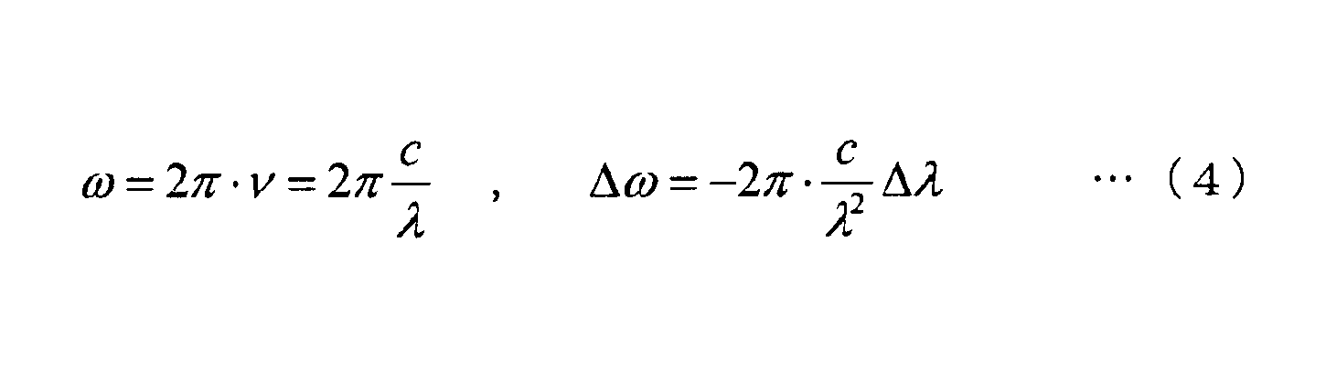


屈折率n(平均屈折率nave)の誘電体層120中を光が時間Δτで移動する距離をΔx’とすると、距離Δx’は、上記式3及び式5を用いて、以下のように表現される。

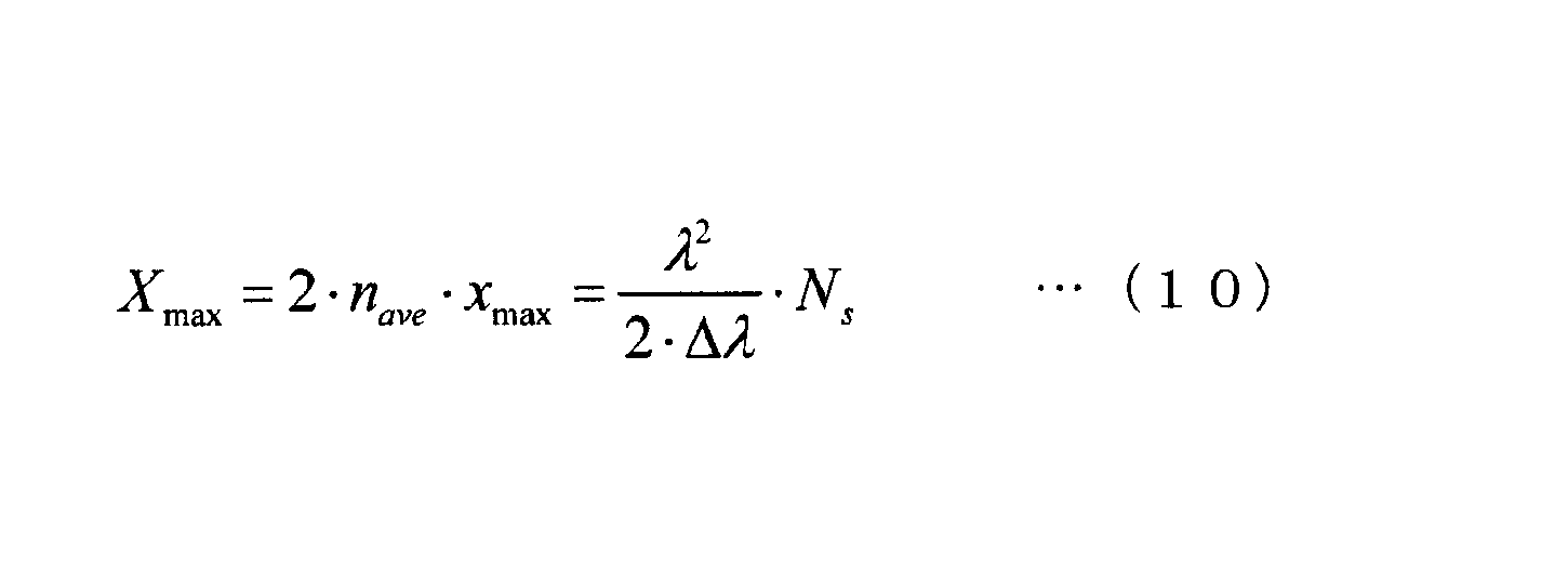


式12により、より厚い測定対象物を測定するためには、波長λ0を長くする手法、波長スパンΔwを狭くする手法が考えられる。しかし、波長λ0をできるだけ長く設定した場合であっても約10%長くする程度が限界である。また、波長スパンΔwをできるだけ狭く設定する場合であっても1桁小さくする程度が限界である。このため、これらのパラメータを変更する手法では、Siに換算して数十mmオーダーの厚さを測定することができない。
一方、式12により、サンプリング数Nsを大きくすれば、より厚い媒質を計測することができる。従来のCCDセンサ等であれば、サンプリング数Nsは配列数であるため固定値であり、変更することが容易ではない。これに対して、チューナブルフィルタ40で反射光の波長を掃引して単一の受光素子41で検出することにより、波長軸方向のサンプリング数Nsをいかようにも設定することができる。例えばサンプリング数Nsを5000等に設定した場合には、512個を配列させたCCDアレイに比べて10倍程度の厚い測定対象物を測定することができる。
また、式12により、分光器の波長範囲Δwを広くすれば、FFT後のデータ間隔ΔXを小さくすることができる。これにより、データ間隔を小さくすることと、計測可能厚さを厚くすることとは、両立しないことがわかる。以上は、屈折率によらない一般式である。よって、屈折率naveの媒質中においての実スケールに変換する場合は、それぞれ2naveで除すればよい。
次に、最小空間分解能について考察する。図10は、最小空間分解能を説明する概要図である。図10の「b」は、ガウス関数で近似できる光源の波数kに依存した強度分布を示すスペクトルである。図10の「b」に示すスペクトルの強度S(k)は、ピーク値の波数をk0、ピーク値の強度を1/Δk・(π)1/2、半値半幅をΔkとすると、以下の式で表すことができる。
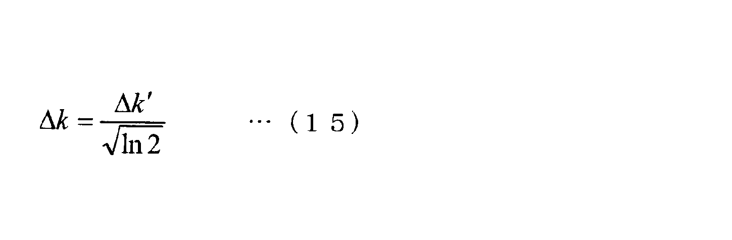


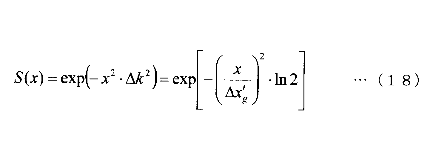
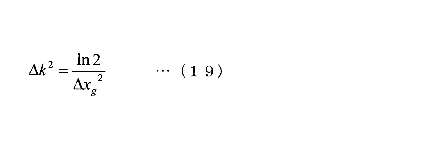

次に、上述した最大計測光学厚さxmaxに基づいて、必要なサンプリング数Nsの条件を導出する。光源10の中心波長をλ0、光源スペクトルの半値半幅をΔλ、チューナブルフィルタ40の波長掃引範囲である波長スパンをΔw、誘電体層120の屈折率をnとすると、式9に基づいて、最大計測光学厚さxmaxは以下の式で表される。



次に、測定対象物の厚さ方向の空間分解能について検討する。例えば、波長域が1200nm~2000nmのSuper Continuum光源を用いた場合、コヒーレンス長は、数式20を用いて0.7umとなる。コヒーレンス長は、ガウス関数の半値半幅となるため、空間分解能はその2倍の1.4um程度とすることができる。一方、周波数ドメイン方式では、SC光源を用いた場合、FFT後のデータ間隔Δxは、式13を用いて3.2umとなる。実空間のデータ間隔Δxは、FFT後のデータ間隔Δxを屈折率nで除算することにより得られるため、例えば、Si(屈折率3.6)であればΔx=0.9um、Qz(屈折率1.46)であればΔx=1.46umとなる。このため、Siであれば1um程度、Qzであれば2um程度の分解能となる。
周波数ドメイン方式を利用した測定対象物の厚さの計測では、FFT後の2ndの位置を正確に求めるために、あえてある程度の幅を持つ2nd信号の重み付け重心を計算する。そして、重み付け重心の位置の変化に基づいて光路長2ndの変化を検出する。ここで、重み付け重心を高精度に求めるためには、FFT後の2ndの信号形状がガウス関数に近く、かつ、半値全幅2lc内に少なくとも3個以上の複数のサンプリング点が必要となる。また、2ndの信号形状がガウス関数となるには、光源スペクトル自体もガウス関数となる必要がある。すなわち、Gaussianスペクトル光源で、かつ、検出範囲内にガウス関数の裾部分が十分に含まれる必要がある。例えば、図11の「a」に示す反射光スペクトルは、ガウス関数に近いスペクトルの一例である。図11の「b」は、図11の「a」に示す反射光スペクトルのFFT後の信号である。このような反射光スペクトルであれば、FFT後の信号形状がガウス関数に近く、裾部分も検出範囲1540~1580nm内に十分含まれているため、適切に重心位置を求めることができる。しかしながら、図12の「a」に示す反射光スペクトルのように、裾部分が検出範囲から大きくはみ出している場合には、図12の「b」に示す信号のようにピークが鋭くなり、重心位置の精度が低下する。また、図13の「a」に示す反射光スペクトルのように、検出範囲の中心と反射光スペクトルの中心波長が異なる場合には、図13の「b」に示す信号のように形状がガウス関数とはならず、重心位置の精度が低下する。
Gaussianスペクトル光源や、任意のGaussianスペクトル光源のための光学フィルタの設計は困難であるため、FFTの実行前にデータ自体を加工することが考えられる。すなわち、任意のスペクトルを有する光源を用いて、サンプルからの反射光スペクトルを得た後、FFTの実行前に、窓関数を用いて反射スペクトルを加工することが考えられる。加工後の信号を反射光スペクトルとして取り扱うことで、FFTの重心の精度を精度良く求めることができる。
窓関数としては例えばガウス関数が用いられる。以下ではガウス関数の一例を説明する。ガウス関数としては、面積を1に規格化するものと、高さを1に規格化するものがある。図14の「a」は、面積を1に規格化するガウス関数の一例である。中心波長をλ0、半値半幅をΔλHWHMとすると、図14の「a」に示すガウス関数は以下のように表現される。

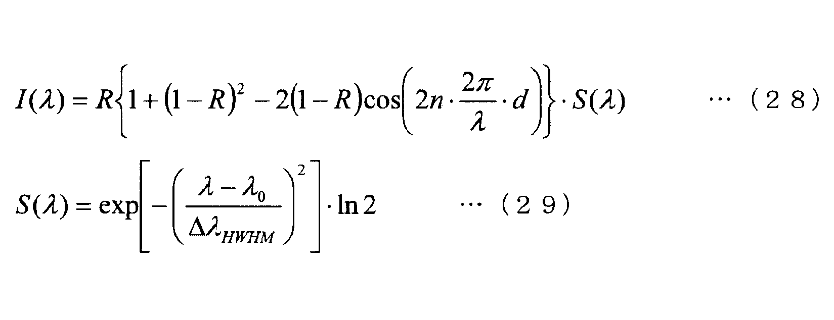

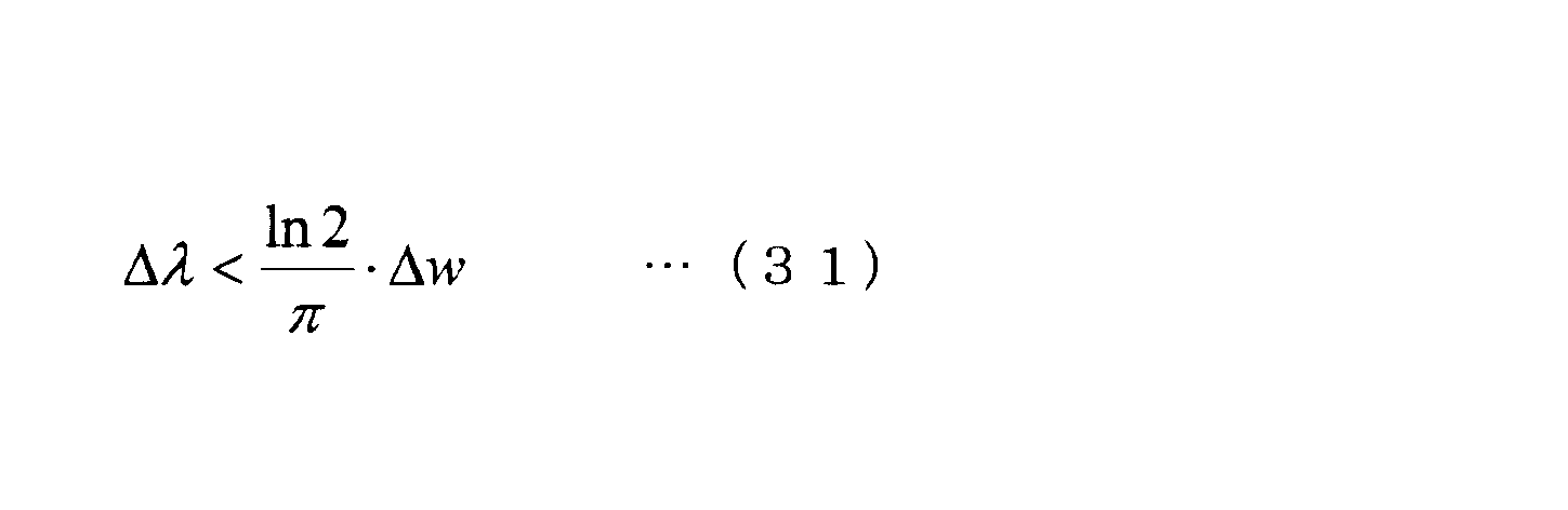
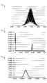
以下では、具体的に窓関数を用いた場合を説明する。図15の「a」は、中心波長λ0=1548nm、半値半幅ΔλHWHM=30nm、サンプル厚さd=775um、サンプルの屈折率n=3.7とした場合の反射光スペクトルの一例である。図15の「b」は、ガウス関数の一例であり、半値半幅ΔλHWHM=5nmである。図15の「c」は、図15の「a」に示す反射光スペクトルに、図15の「b」に示すガウス関数を適用して得られる信号である。
図16の「a」(すなわち図15の「a」)に示すように、中心波長λ0=1548nm、半値半幅ΔλHWHM=30nm、サンプル厚さd=775um、サンプルの屈折率n=3.7とした場合の反射光スペクトルを用いた場合には、FFT後の2nd信号は、図16の「b」に示すものとなる。図16の「c」は、図16の「b」のピーク部分の拡大図である。このように、ピーク自体が1つのサンプリング点のみで決定されているため、重心位置の精度が低下する。
これに対して、図17の「a」(すなわち図15の「c」)に示すように、窓関数を適用した後の信号を用いることで、FFT後の2nd信号は、図17の「b」及び図17の「c」に示すように幅の持ったピークを有することとなる。このため、重心位置の精度を向上させることができる。
また、図18は、光源の半値半幅ΔλHWHMとFFT後の波形の幅との関係を示すグラフである。図18に示すように、光源の半値半幅ΔλHWHMの大きさを変更すると、FFT後の2ndの波形の幅が変化する。FFT後のピーク形状を構成する点が多い程、重心の計算精度が向上する。すなわち、光源の半値半幅ΔλHWHMが小さくなるほどFFT後の2ndの波形の幅を大きくすることができる。
(誘電体層の厚さを計測する方法)
次に、光干渉システム1を用いて誘電体層の厚さを計測する方法について説明する。図19は、光干渉システム1の動作を示すフローチャートである。図19に示す制御処理は、例えば光源10及び演算装置15の電源がオンされたタイミングから所定の間隔で繰り返し実行される。なお、図19の実行前に、チューナブルフィルタ40の事前設定が済んでいるものとする。すなわち、事前に、例えば図6に示すような印加電圧(又は印加周波数)と透過光の波長との関係が取得されているものとする。
次に、光干渉システム1を用いて誘電体層の厚さを計測する方法について説明する。図19は、光干渉システム1の動作を示すフローチャートである。図19に示す制御処理は、例えば光源10及び演算装置15の電源がオンされたタイミングから所定の間隔で繰り返し実行される。なお、図19の実行前に、チューナブルフィルタ40の事前設定が済んでいるものとする。すなわち、事前に、例えば図6に示すような印加電圧(又は印加周波数)と透過光の波長との関係が取得されているものとする。
図19に示すように、反射光スペクトルの入力処理から開始する(S10)。光源10は、測定光を発生する。例えば、図20の「a」に示すスペクトルの測定光となる。受光素子41は、誘電体層120の表面120a及び裏面120bで反射した反射光のスペクトルを取得する。すなわち、チューナブルフィルタ40によって波長掃引しつつ、受光素子41で検出する。これにより、例えば、図20の「b」に示すスペクトルの反射光となる。光路長算出部16は、受光素子41から反射光のスペクトルを入力する。S10の処理が終了すると、波形調整処理へ移行する(S11)。
S11の処理では、波形調整部31が波形を調整する。すなわち、上述した窓関数を反射光スペクトルに適用する。S11の処理が終了すると、座標変換処理へ移行する(S12)。
S12の処理では、光路長算出部16が、S11の処理で得られたスペクトルの座標軸を、波長λから空間周波数(1/λ)へ変換する。例えば、図20の「c」に示すスペクトルとなる。S12の処理が終了すると、第1データ補間処理へ移行する(S14)。
S14の処理では、光路長算出部16が、S12の処理で得られたスペクトルのデータ補間を行う。例えば、サンプリング数をNsとし、スペクトルのデータとして、空間周波数の配列を(x0,x1,x2,…,xNs-1)とし、強度の配列を(y0,y1,y2,…,yNs-1)とする。まず、光路長算出部16は、空間周波数の配列を等間隔に再配列する。例えば、再配列後の空間周波数の配列に含まれる空間周波数をXiとすると、以下の式を用いて再配列を行う。


S16の処理では、フーリエ変換部17が、S14の処理で補間されたスペクトルをフーリエ変換する(フーリエ変換工程)。これにより、例えば、図21の「b」に示すように、縦軸が振幅、横軸が位相のスペクトルとなる。S16の処理が終了すると、フィルタリング処理へ移行する(S18)。
S18の処理では、光路長算出部16が、S16の処理で得られたスペクトルからX=0のピーク値をフィルタリングする。例えば、X=0からX=Z(所定値)までの範囲の強度データYに0を代入する。S18の処理が終了すると、抽出処理へ移行する(S20)。
S20の処理では、光路長算出部16が、S18の処理で得られたスペクトルからX=2ndのピーク値を抽出する。例えば、ピークの最大値をYiとした場合、Yi-10からデータ点を20点抽出する。これは、ピークの中心から裾までのデータを抽出するためである。例えば、ピークの最大値を1としたときに、最大値から0.5までの範囲が含まれるように抽出する。例えば、図21の「c」に示すスペクトルが抽出される。S20の処理が終了すると、第2データ補間処理へ移行する(S22)。
S22の処理では、データ補間部18が、S20の処理で得られた2ndピークのデータを補間する(データ補間工程)。データ補間部18は、例えばデータ点間を補間数NAで等間隔に線形補間する。補間数NAは、例えば必要な精度に基づいて予め設定される。
例えば、以下の数式を用いてデータ補間を行う。
S24の処理では、重心計算部19が、S22の処理で補間されたデータから重心の計算に利用するデータ範囲のみを抽出する。例えば、重心計算部19は、重心計算に使用する閾値をA%とし、ピークの最大強度YMAX×A以下の強度データYに0を代入する。S24の処理が終了すると、重心計算処理へ移行する(S26)。
S26の処理では、重心計算部19が、S24の処理で補間されたデータから重み付け重心を計算する(重み付け重心計算工程)。例えば、以下の式を用いる。

S28の処理では、厚さ算出部20が、S26の処理で得られた光路長ndを測定対象物(ここでは、誘電体層120)の素材の屈折率で割ることで、測定対象の厚さを算出する(厚さ算出工程)。S28の処理が終了すると、図19に示す制御処理を終了する。
以上で図19に示す制御処理を終了する。図19に示す制御処理を実行することで、反射光スペクトルのサンプリング数を任意に設定しつつ、ガウス関数を用いて精度のよい反射光スペクトルとすることができる。さらに、少ないデータ点であっても高精度に測定対象物の厚さを測定することができる。データ補間工程にて直線補間をすることで、FFT後の信号プロファイルに依存することなく、重心位置を決定することができ、高精度で測体対象物の厚さを計測することができる。本実施形態の計測方法による誘電体層120の厚さの計測精度は-6μm~+6μmの範囲であり、誘電体層120の厚みのばらつきの許容範囲の3%以下となるため、十分な精度が得られていることが分かる。
以上、一実施形態に係る光干渉システム1及びその方法によれば、窓関数を用いてフーリエ変換前の波形をフーリエ変換に適した波形とすることができるので、フーリエ変換後のピーク波形にある程度の幅を持たせることが可能となる。よって、ピーク位置の検出精度を向上させることができる。なお、以上に説明した補間方法は、線形補間に限られず、多項式補間であってもよい。
[ドットパターンニング後の評価]
静電チャック100の表面には、ドット形状の凸部が均等に形成されている場合がある。そこで、表面がドット形状の静電チャック100についても、本実施形態に係る誘電体層の厚さの計測方法を使用してその精度を評価した。以下では、ドット形状の凸部が均等に形成されている静電チャック100に近似した構成にするために、静電チャック100の表面をドット形状(円状)にパターニングした後、本実施形態の計測方法を用いて誘電体層の厚さを評価した。
静電チャック100の表面には、ドット形状の凸部が均等に形成されている場合がある。そこで、表面がドット形状の静電チャック100についても、本実施形態に係る誘電体層の厚さの計測方法を使用してその精度を評価した。以下では、ドット形状の凸部が均等に形成されている静電チャック100に近似した構成にするために、静電チャック100の表面をドット形状(円状)にパターニングした後、本実施形態の計測方法を用いて誘電体層の厚さを評価した。
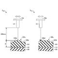
パターニングでは、図22の「a」及び図22の「b」に示したように、ドット120c内の表面120c1は、鏡面とし、ドット120c外の表面120dはサンドブラスト処理により砂面のまま残す。例えば、図22の「a」には、ドット120cの表面120c1から誘電体層120の底面までの厚さdが示されている。
また、コリメータ12からドット120cの表面120c1までの距離200mmが示されている。しかし、コリメータ12からドット120cの表面120c1までの距離はこれに限られない。
図22の「b」に示したように、ドット外の砂面となっている表面120dに測定光(赤外光)を当てると、測定光は散乱してしまう。このため、図22の「a」に示したように、コリメータ12の水平移動が可能な調整機構12aを使用して、コリメータ12を水平移動させ、ドット120cの表面120c1から誘電体層120に光を入射させるようにする。このように、表面にドット形状が形成されている静電チャック100の誘電体層120の厚さの計測では、コリメータ12を移動させてドット形状が形成された位置をスキャニングし、ドット120c内から光を入射する。なお、調整機構12aは、水平移動とともにコリメータ12の角度調整が可能である。これにより、コリメータ12から出力される測定光の誘電体層120への入射角を調整できる。
図1のSTEP3に示したように、誘電体層120の表面120aは研磨により平坦化されているが、電極層110が歪んでいる場合、誘電体層12の表面120aから電極層110(誘電体層12の裏面120b)までの距離は均一ではない。このとき、反射光の強度は、一般的に静電チャック100に垂直に入射している場合に最大となるが、図19のS16のFFT処理後の信号が最大になるとは限らない。計測精度を高めるためには、FFT処理後の信号強度が最も強くなるコリメータ12の入射角をその都度採用することが好ましい。
FFT処理では、矩形窓、ガウス窓、ハミング窓等の窓関数を用いる。窓関数(ここでは、矩形窓)を用いた場合、有限区間外の波形は0と認識され、有限区間終端部分の波形形状がいびつになる。この結果、FFT処理後の信号強度のピークの分解能とダイナミックレンジとの間にトレードオフが存在することになる。
よって、本実施形態では、計測精度を高めるためには、調整機構12aによって角度調整を行って、FFT処理後の信号強度が最も強くなる角度にコリメータ12の入射角を制御することが好ましい。
(ドット内の一点から光を入射させた場合の厚さ計測精度)
以下では、調整機構12aによってコリメータ12を水平移動させ、誘電体層120上に形成されたドット120c内の一点から光を入射させ、本実施形態に係る誘電体層の厚さ計測方法を用いて誘電体層120の厚さを計測した。その結果を図23に示す。横軸は、計測時間(秒)を示し、縦軸は、計測した結果得られた誘電体層120の厚さd(μm)を示す。この結果によれば、厚さdの平均は、385.97μmであり、定常状態での測定精度は、±0.787μmであった。
以下では、調整機構12aによってコリメータ12を水平移動させ、誘電体層120上に形成されたドット120c内の一点から光を入射させ、本実施形態に係る誘電体層の厚さ計測方法を用いて誘電体層120の厚さを計測した。その結果を図23に示す。横軸は、計測時間(秒)を示し、縦軸は、計測した結果得られた誘電体層120の厚さd(μm)を示す。この結果によれば、厚さdの平均は、385.97μmであり、定常状態での測定精度は、±0.787μmであった。
前述したように、誘電体層の厚みは、「誘電体層が絶縁破壊を発生する下限の厚み」以上であって、「静電チャックによって基板を吸着可能な上限の厚み」以下でなければならない。つまり、誘電体層の厚みについては高い設計精度が求められる。これは、一般的な静電チャックの場合、電極層110の表面110aから誘電体層120の表面120aまでの数値は、数百μm程度である。より望ましくは、約200μm以上400μm以下であることを示す。したがって、図1のSTEP3に示した電極層110の歪みαの許容範囲もμmオーダーの分解能で測定する必要がある。このように、誘電体層の厚さを計測する方法には高精度な分解能が要求される。
よって、演算装置15(制御部)は、計測された誘電体層120の厚さが200μm以上400μm以下であるかを判定し、その厚さが200μmより小さい又は400μmより大きい値であった場合には、警告を表示するようにしてもよい。ただし、これに限られず、演算装置15は、計測された誘電体層120の厚さが、予め定められた範囲内にあるかを判定してもよい。予め定められた範囲は、数百μm程度の範囲であってもよい。判定の結果、計測された誘電体層120の厚さが、予め定められた範囲に含まれない場合、警告を表示してもよい。
同様に、演算装置15(制御部)は、誘電体層120の厚さの最大値(Max)と最小値(Min)との差が200μm以下であるかを判定し、200μmより大きい場合には、警告を表示するようにしてもよい。ただし、これに限られず、演算装置15は、計測された誘電体層120の厚さの最大値と最小値との差が、予め定められた閾値以下であるかを判定してもよい。予め定められた閾値は、数百μm程度の値であってもよい。判定の結果、計測された誘電体層120の厚さの最大値と最小値との差が、予め定められた閾値以下である場合、警告を表示してもよい。
以上から、本実施形態に係る誘電体層の厚さの計測方法に対しても測定対象物をμmオーダーの高精度な計測ができることが要求されている。これに対して、図23に示した定常状態での誘電体層120の厚さdの測定精度は、±0.787μmであり、±1μm以下の精度である。これは、本実施形態に係る誘電体層の厚さ計測方法が、誘電体層の厚さの計測に対して十分な精度を有していることを示す。
(ドット内の複数点から光を入射させた場合の厚さ計測精度)
次に、調整機構12aによってコリメータ12を水平方向に微調整させ、同一ドット120c内の複数点から光を入射させた場合の誘電体層120の厚さを計測した。その結果を図24に示す。横軸は、計測時間(秒)を示し、縦軸は、計測した結果得られた誘電体層120の厚さd(μm)を示す。この結果によれば、厚さdは、最小値(Min)と最大値(Max)との間で約11μm変動した。よって、同一ドット内で測定位置を移動させた場合の誘電体層120の厚さdの測定精度は、±5.5μmであった。これは、本実施形態に係る誘電体層の厚さ計測方法は、表面にドット形状を有する誘電体層の厚さの計測に対して、十分な精度を有していることを示す。これによれば、図25の「b」に示したように、一つのドット120c内の平面性を計測することができる。これにより、静電チャック100とウェハとの接触面積による吸着力を予測できる。
次に、調整機構12aによってコリメータ12を水平方向に微調整させ、同一ドット120c内の複数点から光を入射させた場合の誘電体層120の厚さを計測した。その結果を図24に示す。横軸は、計測時間(秒)を示し、縦軸は、計測した結果得られた誘電体層120の厚さd(μm)を示す。この結果によれば、厚さdは、最小値(Min)と最大値(Max)との間で約11μm変動した。よって、同一ドット内で測定位置を移動させた場合の誘電体層120の厚さdの測定精度は、±5.5μmであった。これは、本実施形態に係る誘電体層の厚さ計測方法は、表面にドット形状を有する誘電体層の厚さの計測に対して、十分な精度を有していることを示す。これによれば、図25の「b」に示したように、一つのドット120c内の平面性を計測することができる。これにより、静電チャック100とウェハとの接触面積による吸着力を予測できる。
(ドット形状とフォーカサー)
以上の厚さ計測では、コリメータ12を用いた。コリメータ12は、平行光線として調整された測定光を誘電体層120へ出射する。よって、コリメータ12は、測定対象物までの距離が長いときに有用である。一方、図25に示したように、フォーカサー13は、測定光を集光し、誘電体層120へ出射する。よって、フォーカサー13は、測定対象物までの距離が固定されているときに有用である。例えば、図25の「a」では、焦点距離200mm、ビーム径1mmのフォーカサー13を使用し、スポット径を100μmとした例が示されている。図25の「b」に示したように、許容できるドット120の表面の歪みは静電チャック100を水平とした場合、およそ0.3度となる。
以上の厚さ計測では、コリメータ12を用いた。コリメータ12は、平行光線として調整された測定光を誘電体層120へ出射する。よって、コリメータ12は、測定対象物までの距離が長いときに有用である。一方、図25に示したように、フォーカサー13は、測定光を集光し、誘電体層120へ出射する。よって、フォーカサー13は、測定対象物までの距離が固定されているときに有用である。例えば、図25の「a」では、焦点距離200mm、ビーム径1mmのフォーカサー13を使用し、スポット径を100μmとした例が示されている。図25の「b」に示したように、許容できるドット120の表面の歪みは静電チャック100を水平とした場合、およそ0.3度となる。
よって、フォーカサー13を利用すれば、表面に凹凸のある形状の測定対象物であっても、ピンポイントの厚み計測が可能となる。つまり、本実施形態に係る誘電体層の厚さ計測方法によれば、フォーカサー13を用いることにより、表面にドット形状を有する静電チャック100においても、誘電体層120の厚さを高精度に計測することができる。
加えて、図25の「a」に示したドット径は、2mm程度であるが、図25の「c」に示したように、将来的には、ドット径は数百μm程度になる可能性がある。このように、フォーカサー13を利用すれば、微細なドット120cに測定光を入射することができるため、ピンポイントの厚み計測が可能となる。
(誘電体層の面内厚み分布)
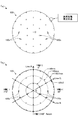
次に、本実施形態に係る誘電体層の厚さ計測方法を用いて、異常放電が発生した誘電体層の厚さを計測した。誘電体層120は円筒状であり、図26の「a」に示したように、誘電体層120の表面は円形である。誘電体層120の表面には、ドット120cが規則的に複数形成されている。
次に、本実施形態に係る誘電体層の厚さ計測方法を用いて、異常放電が発生した誘電体層の厚さを計測した。誘電体層120は円筒状であり、図26の「a」に示したように、誘電体層120の表面は円形である。誘電体層120の表面には、ドット120cが規則的に複数形成されている。
誘電体層120の上部右側(Y軸-60°)の最外周には、異常放電の発生位置が示されている。図26の「b」は、本実施形態における計測位置を示す。計測位置は、ノッチ位置をY軸-180°としてY軸+0°に向かうラインAの軸、ラインAに対して-120°回転させたラインBの軸、ラインAに対して-60°回転させたラインCの軸である。各ライン上に位置するドット120cに測定光を入射させる。各ライン上(つまり、直径方向)に位置するドット120cは、誘電体層120の中心位置Oと、その中心位置Oから半径50mm、半径100mm、半径145.5mmの各周と各ラインが交差する位置に設けられている。よって、各ラインのドット120c上の計測位置は、7箇所となる。
その計測結果を図27の「a」に示す。図27の「a」では、横軸に中心位置O、中心位置Oから±50mm、±100mm、±145.5mmの各計測位置を示し、縦軸に各計測位置における誘電体層120の厚さの計測結果を示す。これによれば、誘電体層120の厚さは、概ね300μm~470μmであり、誘電体層120の厚さのバラツキは、電極層110の歪みの許容範囲である200μm以内に収まっている。ところが、異常放電の発生位置近傍のドット位置120c2では、誘電体層120の厚さは約240μmと最も薄かった。
また、中心位置Oから半径50mm、半径100mm、半径145.5mmの各周方向に位置するドット120cの計測結果を図27の「b」に示す。ノッチ位置(180°)を中心として周方向に位置する複数点のドット位置において誘電体層120の厚さの計測が行われた。計測位置(ドット位置)の個数は、外周側程多くなっている。
この結果、誘電体層120の厚さのバラツキは、半径50mm、半径100mmの周方向では小さく、半径145.5mmの最外周では大きい。つまり、誘電体層120の最外周(半径145.5mm)の電極層110の歪みは、それより内周側に位置する電極層110の歪みよりも大きいことを示している。特に、異常放電の発生位置では、電極層110の歪みが最も大きく、誘電体層120の厚さが最も薄い。以上に示した図27の「a」及び図27の「b」の結果から、異常放電の発生位置と最も誘電体層120の厚さが薄くなった計測位置とが一致した。
さらに、計測後、誘電体層120の表面を研磨することで、誘電体層120の厚さの計測を行った。その結果、本実施形態に係る誘電体層の厚さ計測方法による数値の妥当性が確認された。以上から、本実施形態に係る誘電体層の厚さ計測方法によれば、測定対象物を精度良くかつ非接触で計測することができることが証明された。
以上、光干渉システム及び誘電体層の厚さの計測方法についてその一実施形態を説明したが、本発明に係る光干渉システム及び誘電体層の厚さの計測方法は、上記実施形態に限定されるものではなく、本発明の範囲内で種々の変形及び改良が可能である。また、上記実施例及び変形例を矛盾しない範囲で組み合わせることができる。
例えば、図19に示す制御処理の実行前に、光源スペクトルを事前に取得して記録しておき、S11に示す調整処理の前に、規格化部30によって反射光スペクトルを規格化してもよい。例えば、図28の「a」に示す光源スペクトルを予め取得しているものとする。そして、図28の「b」に示すSi基板の反射光スペクトルを取得したものとする。規格化部30は、光源スペクトルを用いて反射光スペクトルを規格化する。例えば、反射光スペクトルを光源スペクトルで除算して、反射率とする。図29の「a」は反射率に規格化したスペクトルの例である。図29の「a」に示すスペクトルに、図29の「b」に示すガウス関数を積算すると、図29の「c」に示すスペクトルとなる。これにより、FFT後の信号は、完全なガウス関数となる。
また、図2に示すA/D変換部42及び波長制御部43を演算装置15に組み込んでもよい。また、図2に示すチューナブルフィルタ40は、光源10と光サーキュレータ11との間に設けてもよいし、光サーキュレータ11とコリメータ12との間に設けてもよい。また、図2では、チューナブルフィルタ40を用いる例を説明したが、可動グレーティングの分光器を用いる場合であってもよい。図30は、分光器14aが可動グレーディングのスペクトルメータ及び単一の受光素子を備えており、演算装置15及びスペクトルメータが協働して透過光の波長λを制御する。また、図31に示すように、可動グレーディングの分光器として光スペクトラムアナライザを用いてもよい。この場合には、波長-強度のスペクトルが直接取得できる。さらに、図32に示すように、演算装置15が光源10の波長を制御してもよい。例えば、測定対象物の素材等により光源10の波長を変更する。このように、波長の掃引部は何であってもよい。
光源としては、測定光と参照光との干渉が測定できれば、任意の光を使用することが可能である。光源からの光は、少なくとも測定対象物の表面と裏面との間の距離(通常は800~1500μm程度)からの反射光が干渉を生じない程度の光が好ましい。具体的には例えば低コヒーレンス光を用いることが好ましい。低コヒーレンス光とは、コヒーレンス長の短い光をいう。低コヒーレンス光の中心波長は例えば0.3~20μmが好ましく、更に0.5~5μmがより好ましい。また、コヒーレンス長としては、例えば0.1~100μmが好ましく、更に3μm以下がより好ましい。このような低コヒーレンス光を光源として使用することにより、余計な干渉による障害を回避でき、測定対象物の表面又は内部層からの反射光に基づく参照光との干渉を容易に測定することができる。
上記低コヒーレンス光を使用した光源としては、例えばSLD(Super Luminescent Diode)、LED、高輝度ランプ(タングステンランプ、キセノンランプなど)、超広帯域波長光源等を使用することができる。これらの低コヒーレンス光源の中でも、輝度の高いSLD(波長、例えば1300nm)を光源として用いることが好ましい。
基板処理装置に本発明に係る光干渉システム1を搭載することで、ウェハ、フォーカスリング及び対向電極の厚さを計測できる。なお、処理室内に収容されているフォーカスリング又は対向電極等のチャンバ内パーツを測定対象物とする場合には、これらのパーツが測定光に対して透過性を有する材質で形成されている必要がある。例えば、チャンバ内パーツの材質として、シリコン、石英又はサファイア等が用いられる。
本国際出願は、2013年6月7日に出願された日本国特許出願2013-121202号に基づく優先権を主張するものであり、その全内容を本国際出願に援用する。
1…光干渉システム、10…光源、11…光サーキュレータ、12…コリメータ、13…フォーカサー、15…演算装置、16…光路長算出部、17…フーリエ変換部、18…データ補間部、19…重心計算部、20…厚さ算出部、30…規格化部、31…波形調整部、40…チューナブルフィルタ、41…受光素子、42…A/D変換部、43…波長制御部、100…静電チャック、110…電極層、120,130…誘電体層
Claims (9)
- 第1主面及び前記第1主面に対向する第2主面を有する測定対象物の厚さを計測する方法であって、
光源から前記測定対象物を透過する波長を有する測定光を出力する第1のステップと、
コリメータ又はフォーカサーを移動させて、前記コリメータ又はフォーカサーから前記出力した測定光を前記測定対象物の第1主面の計測位置へ出射し、前記第1主面及び前記第2主面からの反射光を前記コリメータ又はフォーカサーへ入射する第2のステップと、
前記コリメータ又はフォーカサーからの反射光を受光素子に入射し、前記受光素子に入射された光の強度を取得し、前記受光素子に入射された光の波長を掃引する第3のステップと、
前記取得した光の強度及び前記掃引した光の波長を用いて、波長に依存した強度分布であって前記第1主面及び前記第2主面からの反射光の強度分布である干渉強度分布を測定する第4のステップと、
前記干渉強度分布をフーリエ変換して得られる波形に基づいて前記測定対象物の厚さを前記測定対象物に非接触に計測する第5のステップと、
を含むことを特徴とする計測方法。 - 前記第2のステップは、
前記測定対象物の第1主面の複数の計測位置に測定光を出射するように、前記コリメータ又はフォーカサーを移動させる、
ことを特徴とする請求項1に記載の計測方法。 - 前記第2のステップは、
前記測定対象物の第1主面に形成された複数の凸部のそれぞれに測定光を出射するように、前記コリメータ又はフォーカサーを移動させる、
ことを特徴とする請求項2に記載の計測方法。 - 前記第2のステップは、
前記測定対象物の第1主面に形成された一の凸部内の複数の計測位置に測定光を出射するように、前記フォーカサーを移動させる、
ことを特徴とする請求項2に記載の計測方法。 - 前記測定対象物は静電チャックの電極層上に設けられた誘電体層であり、
前記第5のステップは、
前記計測された誘電体層の厚さが予め定められた範囲内であるかを判定する、
ことを特徴とする請求項2に記載の計測方法。 - 前記第5のステップは、
前記計測された誘電体層の厚さが200μm以上400μm以下であるかを判定する、
ことを特徴とする請求項5に記載の計測方法。 - 前記測定対象物は静電チャックの電極層上に設けられた誘電体層であり、
前記第5のステップは、
前記計測された誘電体層の厚さの最大値と最小値との差が予め定められた閾値以下であるかを判定する、
ことを特徴とする請求項2に記載の計測方法。 - 前記第5のステップは、
前記計測された誘電体層の厚さの最大値と最小値との差が200μm以下であるかを判定する、
ことを特徴とする請求項7に記載の計測方法。 - 前記第2のステップは、
FFT処理後の信号強度に基づき前記コリメータ又はフォーカサーの角度を制御し、前記測定対象物の第1主面の計測位置へ測定光を所定の入射角で出射する、
ことを特徴とする請求項1に記載の計測方法。
Applications Claiming Priority (2)
| Application Number | Priority Date | Filing Date | Title |
|---|---|---|---|
| JP2013121202A JP6159156B2 (ja) | 2013-06-07 | 2013-06-07 | 測定対象物の厚さ計測方法 |
| JP2013-121202 | 2013-06-07 |
Publications (1)
| Publication Number | Publication Date |
|---|---|
| WO2014196401A1 true WO2014196401A1 (ja) | 2014-12-11 |
Family
ID=52008051
Family Applications (1)
| Application Number | Title | Priority Date | Filing Date |
|---|---|---|---|
| PCT/JP2014/063859 Ceased WO2014196401A1 (ja) | 2013-06-07 | 2014-05-26 | 測定対象物の厚さ計測方法 |
Country Status (2)
| Country | Link |
|---|---|
| JP (1) | JP6159156B2 (ja) |
| WO (1) | WO2014196401A1 (ja) |
Cited By (3)
| Publication number | Priority date | Publication date | Assignee | Title |
|---|---|---|---|---|
| CN110491769A (zh) * | 2018-05-15 | 2019-11-22 | 东京毅力科创株式会社 | 部件的驱动方法和处理装置 |
| US20230213331A1 (en) * | 2022-01-06 | 2023-07-06 | Disco Corporation | Measuring apparatus |
| WO2026078905A1 (ja) * | 2024-10-09 | 2026-04-16 | 三菱電機株式会社 | 測距装置、測距方法及び測距システム |
Families Citing this family (1)
| Publication number | Priority date | Publication date | Assignee | Title |
|---|---|---|---|---|
| JP6437364B2 (ja) * | 2015-03-30 | 2018-12-12 | 株式会社Screenホールディングス | 信号処理方法および画像処理装置 |
Citations (8)
| Publication number | Priority date | Publication date | Assignee | Title |
|---|---|---|---|---|
| JPH06102189A (ja) * | 1992-09-17 | 1994-04-15 | Toshiba Corp | 異物検査装置 |
| JPH06281432A (ja) * | 1993-03-25 | 1994-10-07 | Jasco Corp | 微小角度調整装置 |
| JP2000213919A (ja) * | 1999-01-21 | 2000-08-04 | Jeol Ltd | フ―リエ分光法を用いた厚み測定方法 |
| JP2007048823A (ja) * | 2005-08-08 | 2007-02-22 | Nikon Corp | 位置検出装置、アライメント装置、露光装置及びマイクロデバイスの製造方法 |
| JP2008275552A (ja) * | 2007-05-07 | 2008-11-13 | Covalent Materials Corp | 金属膜の埋設深さ測定方法 |
| JP2012216816A (ja) * | 2011-03-30 | 2012-11-08 | Ngk Insulators Ltd | 静電チャックの製法及び静電チャック |
| JP2013009001A (ja) * | 2012-09-12 | 2013-01-10 | Sumitomo Osaka Cement Co Ltd | 静電チャック装置 |
| JP2013096858A (ja) * | 2011-11-01 | 2013-05-20 | Tokyo Electron Ltd | 光干渉システム、基板処理装置及び計測方法 |
Family Cites Families (1)
| Publication number | Priority date | Publication date | Assignee | Title |
|---|---|---|---|---|
| ITTO20110589A1 (it) * | 2011-07-04 | 2013-01-05 | Avio Spa | Apparecchio e metodo per la determinazione della profondita' efficace di cementazione o nitrurazione di componenti di acciaio, in particolare ingranaggi |
-
2013
- 2013-06-07 JP JP2013121202A patent/JP6159156B2/ja active Active
-
2014
- 2014-05-26 WO PCT/JP2014/063859 patent/WO2014196401A1/ja not_active Ceased
Patent Citations (8)
| Publication number | Priority date | Publication date | Assignee | Title |
|---|---|---|---|---|
| JPH06102189A (ja) * | 1992-09-17 | 1994-04-15 | Toshiba Corp | 異物検査装置 |
| JPH06281432A (ja) * | 1993-03-25 | 1994-10-07 | Jasco Corp | 微小角度調整装置 |
| JP2000213919A (ja) * | 1999-01-21 | 2000-08-04 | Jeol Ltd | フ―リエ分光法を用いた厚み測定方法 |
| JP2007048823A (ja) * | 2005-08-08 | 2007-02-22 | Nikon Corp | 位置検出装置、アライメント装置、露光装置及びマイクロデバイスの製造方法 |
| JP2008275552A (ja) * | 2007-05-07 | 2008-11-13 | Covalent Materials Corp | 金属膜の埋設深さ測定方法 |
| JP2012216816A (ja) * | 2011-03-30 | 2012-11-08 | Ngk Insulators Ltd | 静電チャックの製法及び静電チャック |
| JP2013096858A (ja) * | 2011-11-01 | 2013-05-20 | Tokyo Electron Ltd | 光干渉システム、基板処理装置及び計測方法 |
| JP2013009001A (ja) * | 2012-09-12 | 2013-01-10 | Sumitomo Osaka Cement Co Ltd | 静電チャック装置 |
Cited By (4)
| Publication number | Priority date | Publication date | Assignee | Title |
|---|---|---|---|---|
| CN110491769A (zh) * | 2018-05-15 | 2019-11-22 | 东京毅力科创株式会社 | 部件的驱动方法和处理装置 |
| US20230213331A1 (en) * | 2022-01-06 | 2023-07-06 | Disco Corporation | Measuring apparatus |
| US12264908B2 (en) * | 2022-01-06 | 2025-04-01 | Disco Corporation | Measuring apparatus |
| WO2026078905A1 (ja) * | 2024-10-09 | 2026-04-16 | 三菱電機株式会社 | 測距装置、測距方法及び測距システム |
Also Published As
| Publication number | Publication date |
|---|---|
| JP2014238341A (ja) | 2014-12-18 |
| JP6159156B2 (ja) | 2017-07-05 |
Similar Documents
| Publication | Publication Date | Title |
|---|---|---|
| JP5891006B2 (ja) | 光干渉システム、基板処理装置及び計測方法 | |
| JP5805498B2 (ja) | 温度計測システム、基板処理装置及び温度計測方法 | |
| CN102738039B (zh) | 测量装置以及等离子体处理装置 | |
| TWI497044B (zh) | 溫度測定方法及記憶媒體 | |
| TWI521195B (zh) | 用於測量折射指數之方法,折射指數測量裝置,及用於製造光學元件之方法 | |
| JP6053523B2 (ja) | ファブリーペローフーリエ変換分光計 | |
| JP5993207B2 (ja) | 光干渉システム及び基板処理装置 | |
| KR102330413B1 (ko) | 온도 측정 방법, 기판 처리 시스템 및 기판 처리 장치에 배치되는 부재 | |
| US10184786B2 (en) | Wear amount measuring apparatus and method, temperature measuring apparatus and method and substrate processing system | |
| US9234795B2 (en) | Spectroscopic measurement apparatus capable of quickly measuring a spectral characteristic | |
| JP6159156B2 (ja) | 測定対象物の厚さ計測方法 | |
| KR20150073095A (ko) | 두께·온도 측정 장치, 두께·온도 측정 방법 및 기판 처리 시스템 | |
| JP5199981B2 (ja) | エッチング深さの検出方法並びにエッチングモニター装置及びエッチング装置 | |
| JP2018084434A (ja) | 測定装置及び測定方法 | |
| JP2021060276A (ja) | 温度計測システム及び温度計測方法 | |
| JP5901305B2 (ja) | 光干渉システム、基板処理装置及び測定方法 | |
| JP5888111B2 (ja) | エッチングモニタ装置 | |
| JP6479465B2 (ja) | 基板処理装置及び基板温度測定装置 | |
| JP6207383B2 (ja) | 屈折率分布計測方法、屈折率分布計測装置、及び光学素子の製造方法 | |
| JP2014002068A (ja) | 厚みモニタリング装置、エッチング深さモニタリング装置および厚みモニタリング方法 | |
| CN113795725A (zh) | 非接触式晶片厚度测定装置 | |
| Korol’kov et al. | Spectrophotometric method for measuring the groove depth of calibration reflection gratings | |
| JP2017219470A (ja) | 温度計測システム、基板処理装置及び温度計測方法 | |
| JP2009288159A (ja) | 距離測定装置およびこれを備えた光学干渉計、光学顕微鏡 |
Legal Events
| Date | Code | Title | Description |
|---|---|---|---|
| 121 | Ep: the epo has been informed by wipo that ep was designated in this application |
Ref document number: 14807132 Country of ref document: EP Kind code of ref document: A1 |
|
| NENP | Non-entry into the national phase |
Ref country code: DE |
|
| 122 | Ep: pct application non-entry in european phase |
Ref document number: 14807132 Country of ref document: EP Kind code of ref document: A1 |