WO2014192540A1 - 電力変換装置 - Google Patents
電力変換装置 Download PDFInfo
- Publication number
- WO2014192540A1 WO2014192540A1 PCT/JP2014/062740 JP2014062740W WO2014192540A1 WO 2014192540 A1 WO2014192540 A1 WO 2014192540A1 JP 2014062740 W JP2014062740 W JP 2014062740W WO 2014192540 A1 WO2014192540 A1 WO 2014192540A1
- Authority
- WO
- WIPO (PCT)
- Prior art keywords
- power conversion
- power
- unit
- conversion units
- current
- Prior art date
- Legal status (The legal status is an assumption and is not a legal conclusion. Google has not performed a legal analysis and makes no representation as to the accuracy of the status listed.)
- Ceased
Links
Images


Classifications
-
- H—ELECTRICITY
- H02—GENERATION; CONVERSION OR DISTRIBUTION OF ELECTRIC POWER
- H02M—APPARATUS FOR CONVERSION BETWEEN AC AND AC, BETWEEN AC AND DC, OR BETWEEN DC AND DC, AND FOR USE WITH MAINS OR SIMILAR POWER SUPPLY SYSTEMS; CONVERSION OF DC OR AC INPUT POWER INTO SURGE OUTPUT POWER; CONTROL OR REGULATION THEREOF
- H02M5/00—Conversion of AC power input into AC power output, e.g. for change of voltage, for change of frequency, for change of number of phases
- H02M5/40—Conversion of AC power input into AC power output, e.g. for change of voltage, for change of frequency, for change of number of phases with intermediate conversion into DC
- H02M5/42—Conversion of AC power input into AC power output, e.g. for change of voltage, for change of frequency, for change of number of phases with intermediate conversion into DC by static converters
- H02M5/44—Conversion of AC power input into AC power output, e.g. for change of voltage, for change of frequency, for change of number of phases with intermediate conversion into DC by static converters using discharge tubes or semiconductor devices to convert the intermediate DC into AC
- H02M5/453—Conversion of AC power input into AC power output, e.g. for change of voltage, for change of frequency, for change of number of phases with intermediate conversion into DC by static converters using discharge tubes or semiconductor devices to convert the intermediate DC into AC using devices of a triode or transistor type requiring continuous application of a control signal
- H02M5/458—Conversion of AC power input into AC power output, e.g. for change of voltage, for change of frequency, for change of number of phases with intermediate conversion into DC by static converters using discharge tubes or semiconductor devices to convert the intermediate DC into AC using devices of a triode or transistor type requiring continuous application of a control signal using semiconductor devices only
-
- H—ELECTRICITY
- H02—GENERATION; CONVERSION OR DISTRIBUTION OF ELECTRIC POWER
- H02M—APPARATUS FOR CONVERSION BETWEEN AC AND AC, BETWEEN AC AND DC, OR BETWEEN DC AND DC, AND FOR USE WITH MAINS OR SIMILAR POWER SUPPLY SYSTEMS; CONVERSION OF DC OR AC INPUT POWER INTO SURGE OUTPUT POWER; CONTROL OR REGULATION THEREOF
- H02M7/00—Conversion of AC power input into DC power output; Conversion of DC power input into AC power output
- H02M7/42—Conversion of DC power input into AC power output without possibility of reversal
- H02M7/44—Conversion of DC power input into AC power output without possibility of reversal by static converters
- H02M7/48—Conversion of DC power input into AC power output without possibility of reversal by static converters using discharge tubes with control electrode or semiconductor devices with control electrode
-
- H—ELECTRICITY
- H02—GENERATION; CONVERSION OR DISTRIBUTION OF ELECTRIC POWER
- H02H—EMERGENCY PROTECTIVE CIRCUIT ARRANGEMENTS
- H02H7/00—Emergency protective circuit arrangements specially adapted for specific types of electric machines or apparatus or for sectionalised protection of cable or line systems, and effecting automatic switching in the event of an undesired change from normal working conditions
- H02H7/10—Emergency protective circuit arrangements specially adapted for specific types of electric machines or apparatus or for sectionalised protection of cable or line systems, and effecting automatic switching in the event of an undesired change from normal working conditions for converters; for rectifiers
- H02H7/12—Emergency protective circuit arrangements specially adapted for specific types of electric machines or apparatus or for sectionalised protection of cable or line systems, and effecting automatic switching in the event of an undesired change from normal working conditions for converters; for rectifiers for static converters or rectifiers
- H02H7/122—Emergency protective circuit arrangements specially adapted for specific types of electric machines or apparatus or for sectionalised protection of cable or line systems, and effecting automatic switching in the event of an undesired change from normal working conditions for converters; for rectifiers for static converters or rectifiers for inverters, i.e. DC/AC converters
- H02H7/1225—Emergency protective circuit arrangements specially adapted for specific types of electric machines or apparatus or for sectionalised protection of cable or line systems, and effecting automatic switching in the event of an undesired change from normal working conditions for converters; for rectifiers for static converters or rectifiers for inverters, i.e. DC/AC converters responsive to internal faults, e.g. shoot-through
-
- H—ELECTRICITY
- H02—GENERATION; CONVERSION OR DISTRIBUTION OF ELECTRIC POWER
- H02M—APPARATUS FOR CONVERSION BETWEEN AC AND AC, BETWEEN AC AND DC, OR BETWEEN DC AND DC, AND FOR USE WITH MAINS OR SIMILAR POWER SUPPLY SYSTEMS; CONVERSION OF DC OR AC INPUT POWER INTO SURGE OUTPUT POWER; CONTROL OR REGULATION THEREOF
- H02M1/00—Details of apparatus for conversion
- H02M1/0067—Converter structures employing plural converter units, other than for parallel operation of the units on a single load
- H02M1/008—Plural converter units for generating at two or more independent and non-parallel outputs, e.g. systems with plural point of load switching regulators
-
- H—ELECTRICITY
- H02—GENERATION; CONVERSION OR DISTRIBUTION OF ELECTRIC POWER
- H02M—APPARATUS FOR CONVERSION BETWEEN AC AND AC, BETWEEN AC AND DC, OR BETWEEN DC AND DC, AND FOR USE WITH MAINS OR SIMILAR POWER SUPPLY SYSTEMS; CONVERSION OF DC OR AC INPUT POWER INTO SURGE OUTPUT POWER; CONTROL OR REGULATION THEREOF
- H02M1/00—Details of apparatus for conversion
- H02M1/32—Means for protecting converters other than automatic disconnection
- H02M1/325—Means for protecting converters other than automatic disconnection with means for allowing continuous operation despite a fault, i.e. fault tolerant converters
Definitions
- the present invention quickly separates a failed power conversion unit among a plurality of power conversion units provided in parallel from a DC power supply unit that supplies DC power to each of the power conversion units, and performs other sound power conversions.
- the present invention relates to a power converter capable of operating a unit continuously.
- FIG. 3 is a schematic block diagram of this kind of power converter, and 1 is a DC power supply unit.
- the DC power supply unit 1 includes, for example, a diode circuit or a battery that rectifies and smoothes commercial AC power.
- Reference numerals 2 (2a to 2n) denote a plurality of power conversion units connected in parallel to the DC power supply unit 1 via the DC link unit 3.
- These power conversion units 2 (2a to 2n) are formed of inverter units which convert the DC power supplied from the DC power supply unit 1 into AC power and output the AC power.
- the output terminals 4 (4a to 4n) of the power conversion unit 2 (2a to 2n) are, for example, connected in parallel and used as a power output terminal for a large capacity AC load. Alternatively, a plurality of AC loads are individually connected to the output terminals 4 (4a to 4n) of the plurality of power conversion units 2 (2a to 2n).
- Each of the power conversion units 2 (2a to 2n) is interposed between the positive electrode and the negative electrode of the DC input terminal by connecting two semiconductor switching elements Q1 to Q6 consisting of, for example, IGBTs in series. It comprises three sets of half bridge circuits in parallel. Each of the semiconductor switching elements Q1 to Q6 is alternately on / off driven with a predetermined phase difference for each half bridge circuit to thereby switch a DC voltage applied to the half bridge circuit. And each said power conversion unit 2 (2a-2n) connects each series connection point which is the middle point of the said half bridge circuit to the said output terminal 4 (4a-4n), and outputs three-phase alternating current power of a predetermined voltage Configured to
- D1 to D6 are freewheeling diodes connected in antiparallel to the semiconductor switching elements Q1 to Q6.
- Reference numeral 5 denotes a capacitor provided between the DC input terminals of the power conversion unit 2 (2a to 2n) to stabilize the DC voltage supplied to the power conversion unit 2 (2a to 2n).
- Reference numeral 6 denotes a control circuit for on / off controlling the semiconductor switching elements Q1 to Q6 as described above.
- the power conversion device configured in this way is, for example, as disclosed in detail in Patent Document 1 and the like.
- Patent Document 1 discloses that switches 7 using mechanical contacts are respectively provided as circuit switches in direct current input portions of the plurality of power conversion units 2 (2a to 2n). Furthermore, Patent Document 1 discloses that a DC reactor 8 is interposed in each of the DC link portions 3 between the DC power supply unit 1 and the Patent Document 1. The switch 7 disconnects the failed power conversion unit 2 (2a to 2n) from the DC power supply unit 1 when a failure such as a short circuit occurs in any of the plurality of power conversion units 2 (2a to 2n). In this way, only the remaining sound power conversion units 2 (2a to 2n) can be operated.
- the broken power conversion unit 2 (2a to 2n) is disconnected by the switch 7, another sound power conversion unit 2 (2a to 2n) is connected to the short circuit point of the broken power conversion unit 2 (2a to 2n). Excess current flows in from 2n). Then, the flow of the excessive current may cause the other sound power conversion units 2 (2a to 2n) to be in an overcurrent state.
- the DC reactor 8 limits the rising of the current flowing to the other sound power conversion units 2 (2a to 2n) at the time of occurrence of such a short circuit fault, thereby allowing these sound power conversion units 2 (2a to 2n) to Plays a role in preventing the over current state.
- Patent No. 4726624 gazette
- the response characteristics of the power conversion units 2 (2a to 2n) can not be deteriorated.
- the responsiveness to fluctuation of the input DC voltage during normal operation of each of the power conversion units 2 (2a to 2n) is deteriorated.
- the operation response delay of the switch 7 is generally on the order of several milliseconds, and it can not be said that the response to a short circuit failure is high.
- the present invention has been made in consideration of such circumstances, and an object thereof is to quickly separate a failed power conversion unit from among a plurality of power conversion units provided in parallel from a DC power supply unit, and other soundness. It is an object of the present invention to provide a highly responsive power converter with a simple configuration capable of continuously operating a power conversion unit.
- the power conversion device is provided in parallel with a DC power supply unit and a DC link unit to convert DC power supplied from the DC power supply unit into AC power. And a plurality of power conversion units for outputting.
- a plurality of semiconductor switch elements for individually limiting the power supplied to the power conversion units are individually interposed between the power conversion units and the DC power supply unit.
- the control circuit monitoring the short circuit current generated in each of the power conversion units turns off the semiconductor switch element connected to the power conversion unit in which the short circuit current flows and cuts off the power supply to the power conversion unit It is characterized in that it is configured as follows.
- control circuit is configured to, for example, detect the following current and control the semiconductor switch element to turn off.
- the power conversion is performed from the current supplied from the DC power supply unit to the power conversion unit, the current flowing to the semiconductor switching element constituting the main part of the power conversion unit, or the drop of the DC voltage applied to the semiconductor switching element Short circuit current due to short circuit failure of unit.
- the DC power supply unit is formed of, for example, a voltage control type PWM converter that generates a predetermined DC voltage using a semiconductor switching element such as an IGBT or a MOS-FET.
- a semiconductor switching element such as an IGBT or a MOS-FET.
- Each of the plurality of power conversion units is, for example, an inverter unit that generates three-phase AC power.
- the semiconductor switch element is formed of, for example, an IGBT in which diodes are connected in antiparallel, or a reverse conducting IGBT capable of flowing current in both directions.
- the semiconductor switch element is interposed on at least one of the positive electrode side and the negative electrode side of the DC input unit in each of the power conversion units.
- power is supplied to each of the power conversion units by effectively utilizing the element characteristic itself of the semiconductor switching element interposed between each of the power conversion units and the DC power supply unit.
- Power, in particular the current can be limited. Therefore, it is possible to effectively prevent the overcurrent from flowing unintentionally in the semiconductor switching elements that constitute each of the power conversion units.
- the power conversion unit When a short circuit failure occurs in the power conversion unit, the power is controlled by turning off the semiconductor switch element connected to the power conversion unit in which the failure has occurred under the control of the control circuit.
- the conversion unit can be quickly disconnected from the DC power supply unit.
- the response delay of the semiconductor switching device is generally on the order of several microseconds, the power at which the failure occurs is sufficiently fast compared to the case where a conventional switch using a mechanical contact is used as a circuit switch.
- the conversion unit can be disconnected from the DC power supply unit.
- the problem of the operation response delay of each power conversion unit in the normal state is solved as in the conventional device in which a direct current reactor is interposed in the direct current input portion of each power conversion unit. I will not invite you. Moreover, since a DC reactor is not required, it is not necessary to adjust its inductance, and the operation responsiveness of each of the power conversion units can be made sufficiently fast.
- the power conversion unit in which the short circuit failure has occurred can be quickly disconnected from the DC power supply unit only by turning off the semiconductor switch element. Accordingly, other sound power conversion units can be stably and continuously operated without causing the above-mentioned problem of over-current. Therefore, by using a semiconductor switch element having a current limiting function and a DC link circuit separation function, its operating characteristics are guaranteed while simplifying the overall configuration of the power converter, and the sound power conversion unit continues A large amount of practical effects such as enabling driving can be achieved.
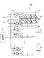
- FIG. 1 is a view showing a schematic configuration of a main part of a power conversion device 10 according to an embodiment of the present invention, and the same parts as those of the conventional power conversion device shown in FIG. In addition, the repetition description is abbreviate
- the DC power supply unit 1 in this embodiment is realized as a voltage control type PWM converter or the like which switches a DC input voltage using a semiconductor switching element such as an IGBT or a MOS-FET to generate a predetermined DC output voltage. Be done.
- the power converter 10 is characterized in that a semiconductor switch element 11 (for example, an IGBT) is provided to each DC input portion of the plurality of power conversion units 2 (2a to 2n) provided in parallel. 11a to 11n) in series as circuit switches. Diodes 12 (12a to 12n) are connected in antiparallel to these semiconductor switch elements 11 (11a to 11n). These diodes 12 (12a to 12n) are alternating current superimposed on direct current power due to the delay of the switching operation of the switching elements Q1 to Q6 mentioned above, variations of the components of the power conversion unit 2 (2a to 2n), etc. Play the role of flowing the crossflow component of
- the semiconductor switch elements 11 (11a to 11n) are interposed in series on the positive electrode side of each DC input portion of the power conversion unit 2 (2a to 2n).
- the semiconductor switch elements 11 (11a to 11n) may be interposed in series on the negative electrode side of the respective DC input portions of the power conversion unit 2 (2a to 2n).
- a reverse conducting IGBT capable of passing current in both directions as the semiconductor switch element 11 (11a to 11n).
- the direct current flowing into each of the power conversion units 2 (2a to 2n) through the semiconductor switch elements 11 (11a to 11n) thus controlled to be on has the element characteristics of the semiconductor switch elements 11 (11a to 11n) Depending on the maximum current is limited. Therefore, the DC power applied to each of the aforementioned half bridge circuits constituting the main part of each of the power conversion units 2 (2a to 2n) is limited. Therefore, an overcurrent does not flow in each half bridge circuit unless an abnormality such as a short circuit occurs in the above-described semiconductor switching elements Q1 to Q6 constituting each half bridge circuit.
- the terminal voltage of the capacitor 5 provided in the DC input portion of the power conversion unit 2 (2a to 2n), that is, the so-called DC link voltage decreases.
- a short circuit current having an abnormally large current value flows from the DC power supply unit 1 to the power conversion unit 2 (2a to 2n).
- the control circuit 6 monitors the occurrence of such a short circuit current through, for example, current detectors 13 (13a to 13n) provided in the DC input unit.
- the control circuit 6 controls the semiconductor switch elements 11 (11a to 11n) in the power conversion unit 2 (2a to 2n) in which the short circuit current is detected to be off.
- the control circuit 6 cuts off the DC power supplied from the DC power supply unit 1 to the power conversion units 2 (2a to 2n).
- the power conversion units 2 (2a to 2n) in which the short circuit failure has occurred are disconnected from the DC power supply unit 1.
- the disconnection of the power conversion unit 2 (2a to 2n) from the DC power supply unit 1 depends on the element characteristics of the semiconductor switch element 11 (11a to 11n), and is performed promptly with only a response delay of several microseconds, for example. Be done.
- the power conversion unit 2 (2a to 2n) in which the short circuit failure has occurred is disconnected. . Therefore, the overcurrent due to the short circuit does not flow into the other sound power conversion units 2 (2a to 2n). Also, even if an overcurrent caused by the short circuit fault flows into the other sound power conversion units 2 (2a to 2n), the current limitation by the semiconductor switch elements 11 (11a to 11n) described above acts. . In this way, the generation of an overcurrent in the sound power conversion unit 2 (2a to 2n) can be prevented in advance. Therefore, the power conversion unit 2 (2a to 2n) in which the short circuit failure has occurred can be separated, and the remaining other healthy power conversion units 2 (2a to 2n) can be continuously operated stably.
- the semiconductor switch elements 11 (11a to 11n) may be used to limit direct current (direct current power) flowing into the power conversion units 2 (2a to 2n). it can.
- the power conversion device 10 having the configuration described above uses the semiconductor switch elements 11 (11a to 11n) at the time of detection of a short circuit current to convert the power conversion unit 2 (2a to 2n) in which the short circuit failure occurs. Can be quickly separated from Therefore, the configuration is simple, and there is an excellent advantage that the operation response characteristic of each of the power conversion units 2 (2a to 2n) in normal operation is not sacrificed.
- each of the power conversion units 2 (2a to 2n) is configured by a three-level inverter as shown in FIG. 2, for example, the following configuration is preferable.
- the semiconductor switch elements 11 (11a to 11n) in series on the positive electrode side of each DC input unit of the power conversion unit 2 (2a to 2n)
- the negative electrode side on each DC input unit The semiconductor switch elements 14 (14a to 14n) are also interposed in series.
- the three-level inverter is also referred to as a neutral point clamp inverter.
- the three-level inverter generally receives the midpoint voltage obtained by dividing the DC output voltage from the DC power supply unit 1 and the positive and negative voltages described above, and the DC voltage between these voltages. Switch the voltage separately. Then, by combining the output voltages obtained by switching among the above-mentioned voltages, AC power closer to a sine wave is generated as compared with the inverter shown in FIG.
- the 3-level inverter is, for example, as described in detail in JP-A-2011-193646.
- reference numerals 15 (15a to 15n) denote diodes connected in antiparallel to the respective semiconductor switch elements 14 (14a to 14n).
- reference numerals 16 (16a to 16n) denote current detectors for detecting currents respectively flowing in the respective semiconductor switch elements 14 (14a to 14n).
- 17a, 17b and 17c denote bi-directional switches for controlling the potential of the series connection point of the half bridge circuits in the three-level inverter.
- the DC power supply unit 1 is equivalently shown as DC power supplies 1a and 1b which output 1/2 DC voltage so as to output the midpoint voltage to be applied to the three-level inverter. Furthermore, in the three-level inverter, two capacitors 5a and 5b interposed between the positive electrode voltage and the intermediate voltage point, and between the intermediate voltage point and the negative electrode voltage point are used.
- the semiconductor switch elements 11 (11a to 11n) and 14 (14a to 14n) are provided on the positive electrode side and the negative electrode side of the unit, respectively.
- the semiconductor switch elements 11 (11a to 11n) on the positive side or the semiconductor switch elements 14 (14a to 14n) on the negative side are turned off in accordance with a short circuit failure on the upper arm side or the lower arm side in each half bridge circuit. Do.
- the power conversion units 2 (2a to 2n) may be disconnected from the DC power supplies 1a and 1b of the DC power supply unit 1, respectively.
- the power conversion unit 2 is controlled under the control of the control circuit 6. It is desirable to disconnect (2a to 2n) also from the other DC power supplies 1a and 1b. In this way, the power conversion unit 2 (2a to 2n) in which the short circuit failure has occurred can be completely disconnected from the DC power supply unit 1. Then, similarly to the embodiment described above, it becomes possible to continue and stably operate the other sound power conversion units 2 (2a to 2n).
- the present invention is not limited to the embodiment described above.
- a MOS-FET or a bipolar transistor as the semiconductor switch elements 11 (11a to 11n) and 14 (14a to 14n) is there.
- a switching element using a SiC (silicon carbide) element.
- the power conversion units 2 (2a to 2n) are provided by the current detectors 13 (13a to 13n) and 16 (16a to 16n) provided at the direct current input portions of the power conversion units 2 (2a to 2n). The short circuit current was detected from the current flowing into the.
- the present invention not only converts power conversion units 2 (2a to 2n) that generate three-phase AC power, but also converts power conversion units 2 (2a to 2n) that generate single-phase AC power and other power conversion circuits in parallel.
- the control circuit 6 detects a short circuit of each of the power conversion units 2 (2a to 2n) to control the semiconductor switch elements 11 (11a to 11n) and 14 (14a to 14n) on / off. It was explained as what to do. However, the on / off control function of the semiconductor switching elements 11 (11a to 11n) and 14 (14a to 14n) based on the short circuit detection can be provided individually for each of the power conversion units 2 (2a to 2n). is there.
- the present invention can be implemented with various modifications without departing from the scope of the invention.
Landscapes
- Engineering & Computer Science (AREA)
- Power Engineering (AREA)
- Inverter Devices (AREA)
- Rectifiers (AREA)
Abstract
Description
特に本発明に係る電力変換装置は、前記各電力変換ユニットと前記直流電源ユニットとの間に、前記各電力変換ユニットに給電される電力を制限する複数の半導体スイッチ素子をそれぞれ個別に介装すると共に、前記各電力変換ユニットに生じる短絡電流をそれぞれ監視する制御回路により、短絡電流が流れた電力変換ユニットに接続された前記半導体スイッチ素子をオフ制御して当該電力変換ユニットに対する電力供給を遮断するように構成したことを特徴としている。
1a,1b 直流電源
2(2a~2n) 電力変換ユニット
3 直流リンク部
5,5a,5b コンデンサ
6 制御回路
10 電力変換装置
11(11a~11n) 半導体スイッチ素子
12(12a~12n) ダイオード
13(13a~13n) 電流検出器
14(14a~14n) 半導体スイッチ素子
15(15a~15n) ダイオード
16(16a~16n) 電流検出器
17a,17b,17c 双方向スイッチ
Q1~Q6 半導体スイッチング素子
D1~D6 フリーホイリング・ダイオード
Claims (5)
- 直流電源ユニットと、
直流リンク部を介して並列に設けられて前記直流電源ユニットから給電される直流電力をそれぞれ交流電力に変換して出力する複数の電力変換ユニットと、
これらの各電力変換ユニットと前記直流電源ユニットとの間にそれぞれ個別に介装されて前記各電力変換ユニットに給電される電力を制限する複数の半導体スイッチ素子と、
前記各電力変換ユニットに生じる短絡電流をそれぞれ監視し、短絡電流が流れた電力変換ユニットに接続された前記半導体スイッチ素子をオフ制御して当該電力変換ユニットに対する電力供給を遮断する制御回路と
を具備したことを特徴とする電力変換装置。 - 前記制御回路は、前記直流電源ユニットから前記電力変換ユニットに供給される電流、前記電力変換ユニットの主体部を構成する半導体スイッチング素子に流れる電流、または前記半導体スイッチング素子に印加される直流電圧の低下から該電力変換ユニットの短絡電流を検出して前記半導体スイッチ素子をオフ制御する請求項1に記載の電力変換装置。
- 前記複数の電力変換ユニットは、それぞれ三相交流電力を生成するインバータ・ユニットである請求項1に記載の電力変換装置。
- 前記半導体スイッチ素子は、前記各電力変換ユニットにおける直流入力部の正極側および負極側の少なくとも一方に介装される請求項1に記載の電力変換装置。
- 前記半導体スイッチ素子は、ダイオードを逆並列に接続したIGBT、または双方向に電流を流し得る逆導通IGBTからなる請求項1に記載の電力変換装置。
Priority Applications (4)
| Application Number | Priority Date | Filing Date | Title |
|---|---|---|---|
| US14/772,411 US10003273B2 (en) | 2013-05-30 | 2014-05-13 | Power conversion device |
| CA2903362A CA2903362C (en) | 2013-05-30 | 2014-05-13 | Power conversion device |
| CN201480012532.5A CN105027415B (zh) | 2013-05-30 | 2014-05-13 | 电力变换装置 |
| SG11201506921WA SG11201506921WA (en) | 2013-05-30 | 2014-05-13 | Power conversion device |
Applications Claiming Priority (2)
| Application Number | Priority Date | Filing Date | Title |
|---|---|---|---|
| JP2013-114721 | 2013-05-30 | ||
| JP2013114721A JP2014236530A (ja) | 2013-05-30 | 2013-05-30 | 電力変換装置 |
Publications (1)
| Publication Number | Publication Date |
|---|---|
| WO2014192540A1 true WO2014192540A1 (ja) | 2014-12-04 |
Family
ID=51988576
Family Applications (1)
| Application Number | Title | Priority Date | Filing Date |
|---|---|---|---|
| PCT/JP2014/062740 Ceased WO2014192540A1 (ja) | 2013-05-30 | 2014-05-13 | 電力変換装置 |
Country Status (7)
| Country | Link |
|---|---|
| US (1) | US10003273B2 (ja) |
| JP (1) | JP2014236530A (ja) |
| CN (1) | CN105027415B (ja) |
| CA (1) | CA2903362C (ja) |
| SG (1) | SG11201506921WA (ja) |
| TW (1) | TWI631809B (ja) |
| WO (1) | WO2014192540A1 (ja) |
Families Citing this family (17)
| Publication number | Priority date | Publication date | Assignee | Title |
|---|---|---|---|---|
| CN104393833A (zh) * | 2014-11-21 | 2015-03-04 | 南车株洲电力机车研究所有限公司 | 一种光伏智能电源 |
| DE102016201735A1 (de) * | 2016-02-04 | 2017-08-10 | Baumüller Nürnberg GmbH | Verfahren zum sicheren Abschalten eines Antriebssystems |
| DE102016117996A1 (de) * | 2016-09-23 | 2018-03-29 | Still Gmbh | Schutzeinrichtung eines Wechselrichters für eine elektrisch angetriebene mobile Arbeitsmaschine |
| CN107919653B (zh) * | 2016-10-10 | 2022-01-11 | 恩智浦有限公司 | 用于开关电路的反向电流保护电路 |
| DE102016123955A1 (de) * | 2016-12-09 | 2018-06-14 | Eaton Industries (Austria) Gmbh | Niederspannungs-Schutzschaltgerät |
| JP6821266B2 (ja) * | 2017-06-26 | 2021-01-27 | 東芝三菱電機産業システム株式会社 | 電力変換装置 |
| JP6943723B2 (ja) * | 2017-10-20 | 2021-10-06 | 株式会社日立製作所 | 電力変換装置及びエレベーター |
| US11177648B2 (en) * | 2017-12-26 | 2021-11-16 | Eaton Intelligent Power Limited | System and method for compact motor control with redundant power structures |
| JP6934823B2 (ja) * | 2018-02-27 | 2021-09-15 | 三菱電機株式会社 | 3レベルiタイプインバータおよび半導体モジュール |
| JP7154907B2 (ja) | 2018-09-14 | 2022-10-18 | 株式会社東芝 | 半導体モジュール |
| JP7102053B2 (ja) * | 2018-12-05 | 2022-07-19 | 日立建機株式会社 | 回生制動システム、及び、それを用いた電気駆動作業車両 |
| JP7224228B2 (ja) * | 2019-04-09 | 2023-02-17 | オムロン株式会社 | モータ駆動装置及びサーボdc給電システム |
| US12301132B2 (en) | 2019-07-23 | 2025-05-13 | Tmeic Corporation | Multiple power conversion system |
| JP2022075146A (ja) * | 2020-11-06 | 2022-05-18 | 株式会社オートネットワーク技術研究所 | Dcdcコンバータ |
| US12348155B2 (en) * | 2021-07-14 | 2025-07-01 | Tmeic Corporation | Power conversion device |
| JP7835527B2 (ja) * | 2022-12-20 | 2026-03-25 | ニチコン株式会社 | 蓄電システム |
| US20250274116A1 (en) * | 2024-02-28 | 2025-08-28 | Advanced Energy Industries, Inc. | Over-current protection for a power supply |
Citations (4)
| Publication number | Priority date | Publication date | Assignee | Title |
|---|---|---|---|---|
| JPS52115323A (en) * | 1976-03-24 | 1977-09-27 | Toshiba Corp | Inverter device |
| JPS57135684A (en) * | 1981-02-17 | 1982-08-21 | Toshiba Corp | Protecting device for inverter |
| JPS62110481A (ja) * | 1985-11-07 | 1987-05-21 | Fuji Electric Co Ltd | 直流配電形インバ−タ装置 |
| JP4726624B2 (ja) * | 2005-12-28 | 2011-07-20 | 東芝三菱電機産業システム株式会社 | インバータシステム |
Family Cites Families (19)
| Publication number | Priority date | Publication date | Assignee | Title |
|---|---|---|---|---|
| JPS5825590U (ja) * | 1981-08-13 | 1983-02-18 | 株式会社三社電機製作所 | インバ−タ装置の保護装置 |
| JPS58154397A (ja) * | 1982-03-05 | 1983-09-13 | Toshiba Corp | インバ−タ装置の並列運転方式 |
| JPH0530793A (ja) * | 1991-07-12 | 1993-02-05 | Yaskawa Electric Corp | サーボ制御装置の地絡検出方法 |
| JP3625692B2 (ja) * | 1999-05-28 | 2005-03-02 | 三菱電機株式会社 | 車載用電力変換装置 |
| JP2000341974A (ja) * | 1999-05-28 | 2000-12-08 | Mitsubishi Electric Corp | 車載用電力変換装置 |
| US6396721B1 (en) | 2000-02-03 | 2002-05-28 | Kabushiki Kaisha Toshiba | Power converter control device and power converter thereof |
| JP2003102180A (ja) * | 2001-09-21 | 2003-04-04 | Hitachi Ltd | 電車用モジュール形インバータ装置 |
| JP3824907B2 (ja) | 2001-11-02 | 2006-09-20 | 東芝三菱電機産業システム株式会社 | 電力変換装置 |
| JP2004015892A (ja) * | 2002-06-05 | 2004-01-15 | Toshiba Corp | インバータの制御装置及び電気自動車 |
| JP4071675B2 (ja) * | 2003-05-27 | 2008-04-02 | 東芝三菱電機産業システム株式会社 | 無停電電源装置の並列運転システム |
| DE102005016177B4 (de) * | 2005-04-08 | 2008-07-03 | Semikron Elektronik Gmbh & Co. Kg | Schaltungsanordnung und zugehöriges Ansteuerverfahren für ein Elektro- oder Hybridfahrzeug mit zwei Gleichstromquellen |
| JP4802153B2 (ja) | 2007-07-30 | 2011-10-26 | 株式会社東芝 | 電気車制御装置 |
| JP2009296844A (ja) | 2008-06-09 | 2009-12-17 | Toyota Motor Corp | 電動車両およびリレー溶着判定方法 |
| JP4772104B2 (ja) | 2008-12-10 | 2011-09-14 | 三菱電機株式会社 | 電力変換装置 |
| DE112011102229T5 (de) * | 2010-06-29 | 2013-06-06 | Honda Motor Co., Ltd. | Elektrisches Automobil |
| WO2012008022A1 (ja) * | 2010-07-14 | 2012-01-19 | トヨタ自動車株式会社 | 車両の制御装置 |
| DE102011015977A1 (de) | 2011-04-04 | 2012-10-04 | Andreas Stihl Ag & Co. Kg | Verfahren zur Inbetriebnahme einer elektronischen Ansteuerschaltung eines elektrischen Motors und Schaltungsanordnung hierzu |
| JP5906679B2 (ja) * | 2011-11-10 | 2016-04-20 | 富士電機株式会社 | 電力変換装置、および過電流保護回路 |
| JP2014166033A (ja) * | 2013-02-25 | 2014-09-08 | Toyota Motor Corp | 電源装置 |
-
2013
- 2013-05-30 JP JP2013114721A patent/JP2014236530A/ja active Pending
-
2014
- 2014-05-13 CA CA2903362A patent/CA2903362C/en active Active
- 2014-05-13 CN CN201480012532.5A patent/CN105027415B/zh not_active Expired - Fee Related
- 2014-05-13 US US14/772,411 patent/US10003273B2/en active Active
- 2014-05-13 SG SG11201506921WA patent/SG11201506921WA/en unknown
- 2014-05-13 WO PCT/JP2014/062740 patent/WO2014192540A1/ja not_active Ceased
- 2014-05-29 TW TW103118807A patent/TWI631809B/zh not_active IP Right Cessation
Patent Citations (4)
| Publication number | Priority date | Publication date | Assignee | Title |
|---|---|---|---|---|
| JPS52115323A (en) * | 1976-03-24 | 1977-09-27 | Toshiba Corp | Inverter device |
| JPS57135684A (en) * | 1981-02-17 | 1982-08-21 | Toshiba Corp | Protecting device for inverter |
| JPS62110481A (ja) * | 1985-11-07 | 1987-05-21 | Fuji Electric Co Ltd | 直流配電形インバ−タ装置 |
| JP4726624B2 (ja) * | 2005-12-28 | 2011-07-20 | 東芝三菱電機産業システム株式会社 | インバータシステム |
Also Published As
| Publication number | Publication date |
|---|---|
| CN105027415A (zh) | 2015-11-04 |
| US20160036342A1 (en) | 2016-02-04 |
| SG11201506921WA (en) | 2015-09-29 |
| CA2903362C (en) | 2022-05-10 |
| JP2014236530A (ja) | 2014-12-15 |
| TWI631809B (zh) | 2018-08-01 |
| CA2903362A1 (en) | 2014-12-04 |
| CN105027415B (zh) | 2018-10-12 |
| US10003273B2 (en) | 2018-06-19 |
| TW201517493A (zh) | 2015-05-01 |
Similar Documents
| Publication | Publication Date | Title |
|---|---|---|
| CA2903362C (en) | Power conversion device | |
| JP6062132B1 (ja) | 電力変換装置および電力システム | |
| JP6009651B2 (ja) | 電力変換装置 | |
| JP6113373B2 (ja) | 電力変換装置 | |
| JP6575289B2 (ja) | 電力変換装置 | |
| US20160294276A1 (en) | Power conversion device | |
| CN108432111B (zh) | Dcdc转换器 | |
| US10530243B2 (en) | Power conversion device with malfunction detection | |
| JP5145124B2 (ja) | 電力変換装置 | |
| JP2015156740A (ja) | 電力変換装置 | |
| CN102934349B (zh) | 用于模块化的多级转换器的双模块 | |
| JP2013059248A (ja) | 3レベル電力変換装置 | |
| KR20200096719A (ko) | 반도체 단락 회로 전도 손실을 감소시키기 위한 3-레벨 펄스 폭 변조 기술 | |
| JP4942169B2 (ja) | 3レベルインバータ装置 | |
| WO2018087891A1 (ja) | 電力変換装置 | |
| Katebi et al. | Advanced three level active neutral point converter with fault tolerant capabilities | |
| JP6700578B2 (ja) | 無停電電源装置 | |
| KR102453339B1 (ko) | 고장 회피 회로를 가지는 멀티레벨 인버터 | |
| JP4575876B2 (ja) | インバータ装置及びインバータシステム | |
| CN210041670U (zh) | 直流电源电路 | |
| WO2013136775A1 (ja) | 直流電源装置 | |
| JP2015100151A (ja) | 電力変換装置 | |
| JP2007181331A (ja) | インバータシステム | |
| JP2000023466A (ja) | インバータ装置 |
Legal Events
| Date | Code | Title | Description |
|---|---|---|---|
| WWE | Wipo information: entry into national phase |
Ref document number: 201480012532.5 Country of ref document: CN |
|
| 121 | Ep: the epo has been informed by wipo that ep was designated in this application |
Ref document number: 14805162 Country of ref document: EP Kind code of ref document: A1 |
|
| ENP | Entry into the national phase |
Ref document number: 2903362 Country of ref document: CA |
|
| WWE | Wipo information: entry into national phase |
Ref document number: 14772411 Country of ref document: US |
|
| NENP | Non-entry into the national phase |
Ref country code: DE |
|
| 122 | Ep: pct application non-entry in european phase |
Ref document number: 14805162 Country of ref document: EP Kind code of ref document: A1 |