WO2014192336A1 - タッチパネル基板 - Google Patents
タッチパネル基板 Download PDFInfo
- Publication number
- WO2014192336A1 WO2014192336A1 PCT/JP2014/054341 JP2014054341W WO2014192336A1 WO 2014192336 A1 WO2014192336 A1 WO 2014192336A1 JP 2014054341 W JP2014054341 W JP 2014054341W WO 2014192336 A1 WO2014192336 A1 WO 2014192336A1
- Authority
- WO
- WIPO (PCT)
- Prior art keywords
- substrate
- electrode
- touch panel
- terminal portion
- sensor electrode
- Prior art date
- Legal status (The legal status is an assumption and is not a legal conclusion. Google has not performed a legal analysis and makes no representation as to the accuracy of the status listed.)
- Ceased
Links
Images



Classifications
-
- G—PHYSICS
- G06—COMPUTING OR CALCULATING; COUNTING
- G06F—ELECTRIC DIGITAL DATA PROCESSING
- G06F3/00—Input arrangements for transferring data to be processed into a form capable of being handled by the computer; Output arrangements for transferring data from processing unit to output unit, e.g. interface arrangements
- G06F3/01—Input arrangements or combined input and output arrangements for interaction between user and computer
- G06F3/03—Arrangements for converting the position or the displacement of a member into a coded form
- G06F3/041—Digitisers, e.g. for touch screens or touch pads, characterised by the transducing means
- G06F3/0416—Control or interface arrangements specially adapted for digitisers
- G06F3/04164—Connections between sensors and controllers, e.g. routing lines between electrodes and connection pads
-
- G—PHYSICS
- G06—COMPUTING OR CALCULATING; COUNTING
- G06F—ELECTRIC DIGITAL DATA PROCESSING
- G06F3/00—Input arrangements for transferring data to be processed into a form capable of being handled by the computer; Output arrangements for transferring data from processing unit to output unit, e.g. interface arrangements
- G06F3/01—Input arrangements or combined input and output arrangements for interaction between user and computer
- G06F3/03—Arrangements for converting the position or the displacement of a member into a coded form
- G06F3/041—Digitisers, e.g. for touch screens or touch pads, characterised by the transducing means
-
- G—PHYSICS
- G06—COMPUTING OR CALCULATING; COUNTING
- G06F—ELECTRIC DIGITAL DATA PROCESSING
- G06F3/00—Input arrangements for transferring data to be processed into a form capable of being handled by the computer; Output arrangements for transferring data from processing unit to output unit, e.g. interface arrangements
- G06F3/01—Input arrangements or combined input and output arrangements for interaction between user and computer
- G06F3/03—Arrangements for converting the position or the displacement of a member into a coded form
- G06F3/041—Digitisers, e.g. for touch screens or touch pads, characterised by the transducing means
- G06F3/0412—Digitisers structurally integrated in a display
-
- G—PHYSICS
- G06—COMPUTING OR CALCULATING; COUNTING
- G06F—ELECTRIC DIGITAL DATA PROCESSING
- G06F3/00—Input arrangements for transferring data to be processed into a form capable of being handled by the computer; Output arrangements for transferring data from processing unit to output unit, e.g. interface arrangements
- G06F3/01—Input arrangements or combined input and output arrangements for interaction between user and computer
- G06F3/03—Arrangements for converting the position or the displacement of a member into a coded form
- G06F3/041—Digitisers, e.g. for touch screens or touch pads, characterised by the transducing means
- G06F3/047—Digitisers, e.g. for touch screens or touch pads, characterised by the transducing means using sets of wires, e.g. crossed wires
-
- H—ELECTRICITY
- H05—ELECTRIC TECHNIQUES NOT OTHERWISE PROVIDED FOR
- H05K—PRINTED CIRCUITS; CASINGS OR CONSTRUCTIONAL DETAILS OF ELECTRIC APPARATUS; MANUFACTURE OF ASSEMBLAGES OF ELECTRICAL COMPONENTS
- H05K9/00—Screening of apparatus or components against electric or magnetic fields
- H05K9/0067—Devices for protecting against damage from electrostatic discharge
-
- G—PHYSICS
- G06—COMPUTING OR CALCULATING; COUNTING
- G06F—ELECTRIC DIGITAL DATA PROCESSING
- G06F2203/00—Indexing scheme relating to G06F3/00 - G06F3/048
- G06F2203/041—Indexing scheme relating to G06F3/041 - G06F3/045
- G06F2203/04102—Flexible digitiser, i.e. constructional details for allowing the whole digitising part of a device to be flexed or rolled like a sheet of paper
-
- G—PHYSICS
- G06—COMPUTING OR CALCULATING; COUNTING
- G06F—ELECTRIC DIGITAL DATA PROCESSING
- G06F2203/00—Indexing scheme relating to G06F3/00 - G06F3/048
- G06F2203/041—Indexing scheme relating to G06F3/041 - G06F3/045
- G06F2203/04107—Shielding in digitiser, i.e. guard or shielding arrangements, mostly for capacitive touchscreens, e.g. driven shields, driven grounds
-
- G—PHYSICS
- G06—COMPUTING OR CALCULATING; COUNTING
- G06F—ELECTRIC DIGITAL DATA PROCESSING
- G06F3/00—Input arrangements for transferring data to be processed into a form capable of being handled by the computer; Output arrangements for transferring data from processing unit to output unit, e.g. interface arrangements
- G06F3/01—Input arrangements or combined input and output arrangements for interaction between user and computer
- G06F3/03—Arrangements for converting the position or the displacement of a member into a coded form
- G06F3/041—Digitisers, e.g. for touch screens or touch pads, characterised by the transducing means
- G06F3/044—Digitisers, e.g. for touch screens or touch pads, characterised by the transducing means by capacitive means
Definitions
- the present invention relates to a touch panel substrate.
- a touch panel substrate that can detect the position of a detection object when a finger or an input pen (detection object) is brought into contact with or close to a display screen is displayed on a mobile phone or a notebook personal computer.
- Electronic devices provided on the display surface of the apparatus are widely used.
- the capacitive touch panel substrate includes a plurality of first sensor electrodes extending in a first direction, an electrode layer formed with a second sensor electrode extending in a second direction orthogonal to the first direction, and a first A touch controller is provided that calculates the position of the detection target based on a change in capacitance formed between the sensor electrode and the second sensor electrode.
- the capacitive touch panel substrate there is a problem that when an external electrostatic voltage is applied to the sensor electrode, malfunction occurs or the touch controller is electrostatically destroyed.
- Patent Document 1 includes an electrode and a lead layer that is individually connected to each electrode. Even if a potential difference due to charging between electrodes occurs in an assembly process or a storage process, damage to the lead layer due to electric discharge occurs. A touchpad having a structure that is easy to prevent and a method of manufacturing the same are disclosed.
- Patent Document 2 discloses a touch panel that can reduce misrecognition caused by malfunction by shielding electromagnetic noise and static electricity entering from the outside.
- FIG. 15 is a schematic diagram of a touch panel of Patent Document 2, (a) is a schematic top view of the touch panel, and (b) is an XX ′ cross-sectional view of (a).
- a plurality of detection electrodes 205 and detection electrodes 205 are electrically connected to the surface 203 of the substrate 202 of the touch panel 200 of Patent Document 2, and detection signals not shown are detected.
- a wiring electrode 207 for transmitting to the circuit is formed.
- a first shielding electrode 208 connected to GND is formed on the outer periphery of the substrate 202 in order to shield noise entering from the outside.
- the plurality of detection electrodes 205 are formed at the center of the substrate 202 to form a detection region 204.
- the wiring electrode 207 is formed outside the detection region 204 to form a wiring region 206, and is integrated into the right side edge of the substrate to form a terminal portion TA.
- the first shielding electrode 208 is formed outside the region including the detection region 204 and the wiring region 206 so as to surround the detection region 204 and the wiring region 206. With this configuration, noise that enters from the end of the substrate 202 is shielded by the first shielding electrode 208 before reaching the wiring electrode 207 or the detection electrode 205, thereby reducing erroneous recognition due to malfunction. it can.
- Japanese Patent Publication Japanese Patent Laid-Open No. 2012-155514 (Released on August 16, 2012)”
- Japanese Patent Publication Japanese Patent Laid-Open No. 2010-218542 (published on September 30, 2010)”
- the first shielding electrode 208 of the touch panel 200 of Patent Document 2 04 is not formed on the entire outer periphery of the substrate 202 so as to completely surround the wiring region 206, but is not formed on a portion where the terminal portion TA is formed on the outer periphery of the substrate 202. Therefore, noise enters from a portion of the outer periphery of the substrate 202 where the first shielding electrode 208 is not provided. As a result, there is a risk of erroneous recognition due to malfunction or destruction of a detection circuit (touch controller) (not shown).
- FIG. 16 is a top view of another example of the touch panel of Patent Document 2.
- FIG. 16 illustration of the detection electrode and the wiring electrode is omitted.
- the touch panel 201 shown in FIG. 16 one end of the first flexible substrate 230 is connected to the terminal portion TA.
- the signal processing IC 231 is mounted on the first flexible substrate 230, and the second flexible substrate 232 is connected to the other end of the first flexible substrate 230.
- the second flexible substrate 232 is connected to a touch controller (not shown).
- a first shielding electrode 208 ′ is formed on the terminal portion TA of the first flexible substrate 230.
- the shielding effect of electromagnetic noise from the outside can be improved as compared with the touch panel 200.
- the first shielding electrode 208 ′ is formed on the first flexible substrate 230 and is not formed on the substrate 202. Therefore, it is not possible to sufficiently shield noise that enters from the outside of the substrate 202 along the surface of the substrate 202 and enters.
- the surface of the substrate 202 on which the detection electrode 205 is formed is used as the detection surface. Therefore, static electricity from the user's finger is transmitted to the detection electrode 205, and a voltage due to static electricity is applied to the touch controller via the first flexible substrate 230 and the second flexible substrate 232. As a result, the touch controller is destroyed.
- the present invention has been made in view of the above-described problems, and an object of the present invention is to provide a detection circuit in which a static voltage is applied by shielding static electricity entering a sensor electrode formation surface of a substrate. An object of the present invention is to provide a touch panel substrate that can prevent destruction.
- a touch panel substrate includes a substrate provided with a plurality of sensor electrodes, a detection circuit electrically connected to the sensor electrodes, the sensor electrodes, and the sensors.
- a touch panel substrate that includes a relay wiring for electrically connecting to a detection circuit and that detects a position of a detection target on a detection surface that is a surface facing the outside, wherein the sensor electrode is the substrate.
- the sensor electrode forming surface is provided with a terminal portion made up of the sensor electrode terminals, and one end of the relay wiring is provided on the sensor electrode forming surface. Is connected to the terminal portion, and a shielding electrode is provided outside the terminal portion on the sensor electrode forming surface.
- a touch panel substrate capable of preventing destruction of a detection circuit due to application of an electrostatic voltage by shielding static electricity that enters the sensor electrode formation surface of the substrate. can do.
- FIG. 10 is a top view of another example of the touch panel of Patent Document 2.
- Embodiment 1 Hereinafter, embodiments of the present invention will be described in detail with reference to FIGS.
- FIG. 1 is a cross-sectional view of the touch panel substrate of the present embodiment.
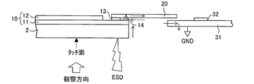
- FIG. 2 is a cross-sectional view showing a connection relationship between the first electrode substrate and the touch controller in the touch panel substrate of the present embodiment.
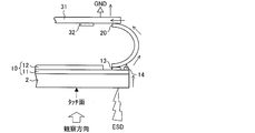
- FIG. 3 is a cross-sectional view showing a connection relationship between the first electrode substrate and the touch controller in a state where the flexible substrate is bent.
- the touch panel substrate 100 includes an AR (Anti Reflection) film 1, a cover glass 2, an OCA (Optical Clear Adhesive, transparent optical adhesive film) 3 and a sensor for preventing reflection of external light.
- the first electrode substrate 10 having electrodes and the protective substrate 4 are stacked in this order.
- the surface of the AR film 1 constitutes a touch surface (detection surface) for detecting contact or proximity of the detection target.
- the AR film 1 is not an essential configuration.
- the surface of the cover glass 2 constitutes the touch surface.
- the surface on the touch surface side is the front surface
- the surface opposite to the front surface is the back surface
- BM (black matrix) 5 is provided on the outer peripheral portion of the back surface of the cover glass 2.
- the BM 5 is provided on the back surface of the cover glass 2 and covering the wiring and the like (not shown) provided on the touch panel substrate 100, the wiring and the like of the touch panel substrate 100 can be prevented from being visually recognized by the user.
- the touch panel substrate 100 can be used as a display device with a touch panel substrate by bonding the protective substrate 4 to the display surface of the display device with the protective substrate 4 facing the display device.
- the first electrode substrate 10 includes a first substrate 11 (substrate), a plurality of sensor electrodes 12, a terminal portion 13 (see FIG. 2) including connection terminals of the sensor electrodes 12, and a shielding electrode 14. .
- the sensor electrode 12, the terminal portion 13, and the shielding electrode 14 are formed on the back surface (sensor electrode formation surface) of the first substrate 11.
- One end of the flexible substrate 20 (relay wiring) is connected to the terminal portion 13.
- the shielding electrode 14 is provided outside the terminal portion 13 on the back surface of the first substrate 11.
- the touch panel substrate 100 includes a touch controller substrate 31 different from the first substrate 11, and a touch controller 32 (detection circuit) as an AFE (analog front end) provided on the touch controller substrate 31. IC).
- the other end of the flexible substrate 20 is connected to the touch controller substrate 31, whereby the plurality of sensor electrodes 12 and the touch controller 32 are electrically connected to each other. If the sensor electrode 12 formed on the first substrate 11 and the touch controller 32 formed on the touch controller substrate 31 can be electrically connected, the flexible substrate 20 is not necessarily used. Both may be connected using a rigid substrate.
- the flexible substrate 20 includes a ground terminal (GND terminal) that is grounded by being connected to the GND of the touch controller substrate 31, and the GND terminal is electrically connected to the shielding electrode 14 in the first substrate 11. .
- GND terminal ground terminal
- static electricity that flows from the touch surface (the front surface of the AR film 1 or the cover glass 2) to the back surface of the first substrate 11 via the side surface of the touch panel substrate 100 is shielded by the shielding electrode 14 before entering the terminal portion 13.
- the potential can be released to the GND potential via the GND terminal of the flexible substrate 20.
- electrostatic breakdown of the touch controller 32 due to application of static voltage can be prevented.
- the shield electrode 14 may not be electrically connected to the GND, but may be provided as a lightning rod.
- an electrostatic removal sheet may be connected to the shielding electrode 14 and the static electricity may be discharged into the air using the electrostatic removal sheet. Thereby, the same effect as the case where the static electricity charged in the shielding electrode 14 is released to the GND can be obtained.
- the flexible substrate 20 may be folded, and the touch controller substrate 31 and the touch controller 32 may be disposed on the back side of the first electrode substrate 10. Thereby, the touch panel substrate 100 can be reduced in size.
- a capacitance is formed between the plurality of sensor electrodes 12.
- a detection object such as a human finger contacts or approaches the detection surface
- the magnitude of the capacitance formed between the two different sensor electrodes 12 changes.
- the touch controller 32 By detecting this change in capacitance using the touch controller 32, the contact position or proximity position of the detection target object on the detection surface of the touch panel substrate 100 can be specified.
- a known circuit can be used as the touch controller 32 for detecting the coordinate position of the detection target.
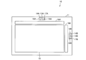
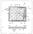
- FIG. 4 is a plan view showing the back side of the first electrode substrate according to an example of the present embodiment.
- a sensor active area 15 in which a plurality of sensor electrodes are formed is provided on the back surface of the first substrate 11.
- the sensor active area 15 is formed with a plurality of first sensor electrodes extending in the first direction and a plurality of second sensor electrodes extending in a second direction orthogonal to the first direction. ing.
- a wiring area 16A for aggregating the wirings connected to each of the plurality of first sensor electrodes and a wiring for aggregating the wirings connected to each of the plurality of second sensor electrodes A wiring area 16B is provided.
- a plurality of connection terminals 17A extended from the first sensor electrode outside the wiring area 16A constitute a terminal portion 13A, and a plurality of connection terminals 17A extended from the second sensor electrode outside the wiring area 16B.
- the connecting terminal 17B constitutes the terminal portion 13B.
- a shielding electrode 14A is provided outside the terminal portion 13A so as to cover the width of the terminal portion 13A, and outside the terminal portion 13B so as to cover the width of the terminal portion 13B. Is provided with a shielding electrode 14B. More specifically, the shielding electrode is provided between the terminal portion and the outer edge of the first substrate 11.
- the terminal portion 13A is connected to one end of the flexible substrate by pressure bonding using an ACF (Anisotropic Conductive Film), and the terminal portion 13B is connected to one end of another flexible substrate by pressure bonding using the ACF.
- ACF Adisotropic Conductive Film
- the flexible substrate includes a plurality of electrode terminals connected to each of the connection terminals 17A (17B) of the terminal portion 13A (13B), and two GND terminals 18.
- the flexible substrate is connected to the back surface of the first substrate 11 such that the two GND terminals 18A are connected to the shielding electrode 14A and the two GND terminals 18A sandwich the terminal portion 13A.
- the other flexible substrate is connected to the back surface of the first substrate 11 such that the two GND terminals 18B are connected to the shielding electrode 14B and the two GND terminals 18B sandwich the terminal portion 13B.
- the terminal portion 13A is surrounded by the two GND terminals 18A and the shielding electrode 14A
- the terminal portion 13B is surrounded by the two GND terminals 18B and the shielding electrode 14B.
- the shielding electrode 14A is provided outside the terminal portion 13A, and the shielding electrode 14B is provided outside the terminal portion 13B. Therefore, as shown in FIG. 1, it is possible to prevent the static electricity that has entered the back surface side of the first substrate 11 from the touch surface of the touch panel substrate 100 from entering the terminal portions 13A and 13B. As a result, it is possible to prevent static voltage from being applied to the touch controller 32 via the terminal portion 13 and the flexible substrate 20. Thereby, the electrostatic breakdown of the touch controller 32 can be prevented.
- the shielding electrodes 14A and 14B are provided only outside the terminal portions 13A and 13B.
- the shielding electrodes 14A and 14B may be provided so as to surround the entire sensor active area 15 and the wiring areas 16A and 16B.
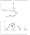
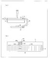
- FIG. 5 is a diagram for explaining a path of static electricity
- (a) is a cross-sectional view of a touch panel substrate of a comparative example showing a path of static electricity when no shielding electrode is provided on the first substrate
- These are top views of the 1st electrode substrate of the touchscreen board
- FIG. 6 is a diagram for explaining a path of static electricity
- (a) is a cross-sectional view of a touch panel substrate of Patent Document 2 as a comparative example
- (b) is a case where a shielding electrode is provided on the first substrate. It is a top view of the 1st electrode substrate of the touch panel substrate of patent document 2 which shows the path
- the first substrate 11 when the first substrate 11 is not provided with a shielding electrode, for example, when a charged user's finger touches the touch surface, the first substrate 11 wraps around the back surface of the first substrate 11. Static electricity enters the terminal portion 13. As a result, a static voltage is applied to the touch controller 32 via the terminal portion 13 and the flexible substrate 20, and the touch controller 32 is electrostatically broken.
- the sensor electrode 12 is formed on the front surface of the first substrate 11. Therefore, static electricity from the outside enters the terminal portion of the terminal portion 13 through the sensor electrode 12. As a result, a static voltage is applied to the touch controller 32 via the terminal portion 13 and the flexible substrate 20, and the touch controller 32 is electrostatically broken.
- the terminal portion 13A is interposed via the sensor electrode 12 inside the shielding electrode 14A. Break into. Therefore, application of static voltage to the touch controller 32 cannot be prevented.
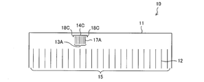
- FIG. 7 is a plan view showing the back side of the first electrode substrate according to another example of the present embodiment.
- the first electrode substrate 10 according to the present embodiment is provided with two GND terminals 18C so as to sandwich the terminal portion 13A as shown in FIG. 7 by connecting a flexible substrate to the back surface of the first substrate 11. It is done.
- the GND terminal 18C of the present embodiment is shorter than the GND terminal 18A of the first embodiment, and is provided so as to sandwich the terminal portion 13A only at the tip portion of the terminal portion 13A. Thus, it is not necessary to provide the GND terminal 18C so as to sandwich both sides of the terminal portion 13A, and it is only necessary to provide the GND terminal 18C so as to be connected to at least the shielding electrode 14C.
- the first electrode substrate according to the present embodiment similarly to the first embodiment, it is possible to prevent the electrostatic voltage from being applied to the touch controller and to prevent the electrostatic breakdown of the touch controller.
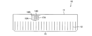
- FIG. 8 is a plan view showing the back side of the first electrode substrate according to still another example of the present embodiment.
- a GND terminal 18D is provided along the connection terminal 17A of the terminal portion 13A by connecting a flexible substrate to the back surface of the first substrate 11. It is done.
- the distance between the GND terminal 18D and the connection terminal 17A closest to the GND terminal 18D is larger than the interval between the adjacent connection terminals 17A.
- the first electrode substrate according to the present embodiment similarly to the first embodiment, it is possible to prevent the electrostatic voltage from being applied to the touch controller and to prevent the electrostatic breakdown of the touch controller.
- the first electrode substrate 10 according to the present embodiment can prevent a short circuit between the GND terminal 18D and the connection terminal 17A.
- electrostatic discharge between the GND terminal 18D and the connection terminal 17A can be suppressed. Therefore, it is possible to more effectively prevent static electricity from entering the terminal portion 13A.
- two GND terminals may be provided so as to sandwich the terminal portion 13A as in the configuration of the first or second embodiment.
- FIG. 9 is a plan view showing the back side of the first electrode substrate according to yet another example of the present embodiment.
- the first electrode substrate 10 is provided with a substantially U-shaped shielding electrode 14E on the back surface of the first substrate 11 so as to cover the outside of the terminal portion 13A.
- the GND terminal 18E of the flexible substrate is connected to the shielding electrode 14E as shown in FIG.
- the first electrode substrate according to the present embodiment similarly to the first embodiment, it is possible to prevent electrostatic voltage from being applied to the touch controller, and to prevent electrostatic breakdown of the touch controller.
- two GND terminals may be provided so as to sandwich the terminal portion 13A as in the configuration of the first or second embodiment.
- FIG. 10 is a plan view showing the back side of the first electrode substrate according to yet another example of the present embodiment.
- the first electrode substrate 10 according to the present embodiment is provided with two GND terminals 18F so as to sandwich the terminal portion 13A as shown in FIG. 10 by connecting a flexible substrate to the back surface of the first substrate 11. It is done.
- the two GND terminals 18F are connected to the shielding electrode 14F, and the length of the shielding electrode 14F is longer than the distance between the two GND terminals 18F.
- the first electrode substrate according to the present embodiment similarly to the first embodiment, it is possible to prevent the electrostatic voltage from being applied to the touch controller and to prevent the electrostatic breakdown of the touch controller.
- FIG. 11 is a diagram showing the configuration of the shielding electrode, (a) is a plan view showing the back side of the first electrode substrate according to still another example of the present embodiment, and (b) is a comparative example. It is a top view which shows the back side of the 1st electrode substrate.
- the first electrode substrate 10 is provided with a shielding electrode 14G on the back surface of the first substrate 11.
- a shielding electrode 14G has a multiple structure having a first shielding electrode 141G, a second shielding electrode 142G, and a third shielding electrode 143G in plan view.
- each shielding electrode 141G to 143G plays a role of buffering against static electricity, to the terminal portion 13A. Intrusion of static electricity can be prevented more reliably. Thereby, it is possible to effectively prevent the electrostatic voltage from being applied to the touch controller, and it is possible to more reliably prevent the electrostatic breakdown of the touch controller.
- FIG. 12 is a cross-sectional view of the touch panel substrate of the present embodiment.
- the touch panel substrate 101 is different from the touch panel substrate 100 of the first embodiment in that a second electrode substrate 40 is provided between the first electrode substrate 10 and the protective substrate 4.
- the second electrode substrate 40 includes a second substrate 41 (substrate), a plurality of sensor electrodes 42, a terminal portion, and a shielding electrode 44.
- the sensor electrode 42, the terminal portion, and the shielding electrode 44 are formed on the back surface (sensor electrode formation surface) of the second substrate 41.
- one end of the flexible substrate 50 (relay wiring) is connected to a terminal portion including a connection terminal of the sensor electrode 42.
- the shielding electrode 44 is provided outside the terminal portion in the second substrate 41.
- the touch panel substrate 101 includes a touch controller substrate 31 different from the first substrate 11 and the second substrate 41, and a touch controller 32 provided on the touch controller substrate 31.
- the other end of the flexible substrate 20 and the other end of the flexible substrate 50 are electrically connected to the touch controller 32, whereby the sensor electrode 12, the sensor electrode 42, and the touch controller 32 are electrically connected to each other. ing.
- the flexible substrate 20 and the flexible substrate 50 include a GND terminal electrically connected to the GND of the touch controller substrate 31, and the GND terminal of the flexible substrate 20 is electrically connected to the shielding electrode 14 in the first substrate 11.
- the GND terminal of the flexible substrate 50 is electrically connected to the shielding electrode 44 in the second substrate 41.
- the structure of each Example of Embodiment 1 is employable.
- FIG. 13 is a plan view of a touch panel substrate according to an example of the present embodiment.
- FIG. 13A is a plan view of the touch panel substrate when the first electrode substrate and the second electrode substrate are overlaid.
- ) Is a plan view of the first electrode substrate
- (c) is a plan view of the second electrode substrate.
- a sensor active area 15 in which a plurality of sensor electrodes 12 are formed is provided on the back surface of the first substrate 11.
- the plurality of connection terminals 17 ⁇ / b> A extended from the sensor electrode 12 constitute a terminal portion 13 ⁇ / b> A.
- a shielding electrode 44I1 is provided outside the terminal portion 13A.
- two GND terminals 18I are provided so as to sandwich the terminal portion 13A.
- shielding electrodes 14I2 that are substantially parallel to the direction in which the sensor electrode 12 extends are provided so as to sandwich the sensor active area 15.
- a sensor active area 45 in which a plurality of sensor electrodes 42 perpendicular to the sensor electrode 12 is formed is provided on the back surface of the second substrate 41.
- the plurality of connection terminals 47A extended from the sensor electrode 42 constitute a terminal portion 43A.
- a shielding electrode 14I1 is provided outside the terminal portion 43A.
- two GND terminals 48I are provided so as to sandwich the terminal portion 43A.
- two shielding electrodes 44I2 that are substantially parallel to the direction in which the sensor electrode 42 extends are provided so as to sandwich the sensor active area 45.
- the shielding electrode 14I2 is below the terminal portion 43A. Running through the layers. In other words, the terminal portion 43A and the shielding electrode 14I2 overlap in plan view.
- the touch panel substrate according to the present embodiment similarly to the first embodiment, it is possible to prevent the electrostatic voltage from being applied to the touch controller and to prevent the electrostatic breakdown of the touch controller.
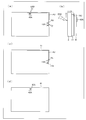
- FIG. 14 is a plan view of a touch panel substrate according to an example of the present embodiment.
- FIG. 14A is a plan view of the touch panel substrate when the first electrode substrate and the second electrode substrate are overlaid.
- (c) is a plan view of the first electrode substrate
- (d) is a plan view of the second electrode substrate. It is.
- the sensor electrode is not shown for the sake of simplicity.
- the cover glass 2, the first substrate 11, and the second substrate 41 constituting the touch surface are provided in this order.
- connection terminals 17A extended from the sensor electrode constitute a terminal portion 13A, and the outside of the terminal portion 13A is shielded.
- An electrode 14J is formed.
- a GND terminal 18J connected to the shield electrode 14J is formed along the connection terminal 17A.
- connection terminals 47A extended from the sensor electrodes constitute a terminal portion 43A.
- the shielding electrode 14J and the GND terminal 18J are formed only on the first substrate 11 which is the substrate closer to the cover glass 2 out of the first substrate 11 and the second substrate 41.
- the electrostatic voltage applied to the touch surface can be released to the GND potential via the shield electrode 14J as shown in FIG. Therefore, it does not enter the back surface of the second substrate 41. Therefore, it is possible to prevent electrostatic voltage from being applied to the touch controller via the terminal portion and the flexible substrate. Thereby, electrostatic breakdown of the touch controller can be prevented.
- the manufacturing cost can be reduced.
- the touch panel substrate according to the first aspect of the present invention includes a substrate (first substrate 11 and second substrate 41) provided with a plurality of sensor electrodes (12, 42), and a detection circuit electrically connected to the sensor electrodes. (Touch controller 32) and a relay surface (flexible substrates 20, 50) for electrically connecting the sensor electrode and the detection circuit, and a detection surface (touch surface) that faces the outside ) In which the sensor electrode is provided on a sensor electrode formation surface that is the surface opposite to the detection surface, and the sensor electrode formation is performed.
- the surface is provided with terminal portions (13, 43) composed of terminals of the sensor electrode, and one end of the relay wiring is connected to the terminal portion, In over the electrode forming surface, on the outside of the terminal section, characterized in that the shielding electrode (14, 44) is provided.
- the static electricity that flows from the side surface of the touch panel substrate to the sensor electrode formation surface of the substrate can be shielded by the shielding electrode before entering the terminal portion.
- the shielding electrode For example, when a charged user's finger touches the detection surface, static electricity that has flowed from the detection surface to the sensor electrode formation surface side can be shielded by the shielding electrode.
- the touch panel substrate according to aspect 2 of the present invention may be a flexible substrate in which the relay wiring is foldable in aspect 1 described above.
- the position where the detection circuit is provided with respect to the sensor electrode forming surface is not limited within the movable range of the flexible substrate. Therefore, for example, the touch panel substrate can be reduced in size by providing the detection circuit on the back surface of the substrate.
- the shielding electrode may be grounded.
- the static electricity shielded by the shielding electrode can be released to the GND.
- the relay wiring includes a ground terminal connected to the shielding electrode.
- the sensor electrode and the terminal portion are , And may be surrounded by the shielding electrode and the ground terminal.
- At least a part of the shielding electrode may be provided in multiples in a plan view on the sensor electrode forming surface.
- a touch panel substrate according to Aspect 6 of the present invention is the second substrate provided in any one of Aspects 1 to 5, provided on the opposite side of the detection surface with respect to the substrate, and facing the substrate.
- the sensor electrode extending surface in the first direction is formed on the sensor electrode forming surface of the substrate, and the second substrate has a second direction orthogonal to the first direction.
- a second sensor electrode extending in the direction may be formed.
- Static electricity that has entered the sensor electrode forming surface side from the detection surface is shielded by a shielding electrode provided on the substrate closer to the detection surface. Therefore, in order to shield the static electricity that has entered the sensor electrode formation surface side from the detection surface, it is not necessary to provide a shielding electrode on the second substrate, which is a substrate far from the detection surface. Since it is not necessary to provide a shielding electrode on the second substrate, the configuration for shielding static electricity can be simplified.
- the present invention can be used for a touch panel substrate used in a mobile phone, a notebook personal computer, or the like.
- First substrate 41
- Second substrate 12
- Sensor electrode 13, 13A, 13B, 43A Terminal portion 14, 14A to J, 44, 44I Shielding electrode 17A, 17B, 47A Connection terminal 18, 18A to 18J, 48I GND terminal 20, 50 Flexible substrate
- Touch controller Detection circuit 100
- 101 Touch panel substrate 101 Touch panel substrate
Landscapes
- Engineering & Computer Science (AREA)
- General Engineering & Computer Science (AREA)
- Theoretical Computer Science (AREA)
- Human Computer Interaction (AREA)
- Physics & Mathematics (AREA)
- General Physics & Mathematics (AREA)
- Computer Networks & Wireless Communication (AREA)
- Microelectronics & Electronic Packaging (AREA)
- Position Input By Displaying (AREA)
Abstract
Description
04と配線領域206とを完全に囲うように基板202の全外周に形成されているのではなく、基板202の外周において端子部TAが形成されている部分には形成されていない。そのため、基板202の外周において第1遮蔽電極208が設けられていない部分からノイズが侵入する。その結果、誤作動に起因する誤認識を生じたり図示しない検出回路(タッチコントローラー)が破壊されたりするおそれがある。
以下、本発明の実施の形態について、図1~6に基づいて詳細に説明する。
ネル基板100においてARフィルム1は必須の構成ではない。ARフィルム1を用いない場合、カバーガラス2の表面がタッチ面を構成する。
図4は、本実施形態の一実施例に係る第1電極基板の背面側を示す平面図である。
、図1に示すように、タッチパネル基板100のタッチ面から第1基板11の背面側に回り込んだ静電気の、端子部13A・13Bへの侵入を防止することができる。その結果、端子部13およびフレキシブル基板20を介してタッチコントローラー32に静電気の電圧が印加されることを防止することができる。これにより、タッチコントローラー32の静電破壊を防止することができる。
図5は静電気の経路を説明するための図であり、(a)は第1基板に遮蔽電極を設けていない場合の静電気の経路を示す比較例のタッチパネル基板の断面図であり、(b)は第1基板に遮蔽電極を設けた場合の静電気の経路を示す本実施形態のタッチパネル基板の第1電極基板の平面図である。
以下、本実施形態の他の実施例について、図7~11に基づいて説明する。なお、説明の便宜上、前記実施例にて説明した部材と同じ機能を有する部材については、同じ符号を
付記し、その説明を省略する。
図8は、本実施形態のさらに他の実施例に係る第1電極基板の背面側を示す平面図である。
図9は、本実施形態のさらに他の実施例に係る第1電極基板の背面側を示す平面図である。
ができる。
図10は、本実施形態のさらに他の実施例に係る第1電極基板の背面側を示す平面図である。
図11は、遮蔽電極の構成を示す図であり、(a)は本実施形態のさらに他の実施例に係る第1電極基板の背面側を示す平面図であり、(b)は比較例としての第1電極基板の背面側を示す平面図である。
本発明の他の実施形態について、図12に基づいて説明すれば、以下のとおりである。なお、説明の便宜上、前記実施形態にて説明した部材と同じ機能を有する部材については、同じ符号を付記し、その説明を省略する。
図13は、本実施形態の一実施例に係るタッチパネル基板の平面図であり、(a)は第1電極基板と第2電極基板とを重ねたときのタッチパネル基板の平面図であり、(b)は第1電極基板の平面図であり、(c)は第2電極基板の平面図である。
図14は、本実施形態の一実施例に係るタッチパネル基板の平面図であり、(a)は第1電極基板と第2電極基板とを重ねたときのタッチパネル基板の平面図であり、(b)は第1電極基板と第2電極基板とを重ねたときのタッチパネル基板の断面図であり、(c)は第1電極基板の平面図であり、(d)は第2電極基板の平面図である。なお、図14においては、説明を簡略化するためにセンサー電極の図示を省略している。
本発明の態様1に係るタッチパネル基板は、複数のセンサー電極(12、42)が設け
られた基板(第1基板11、第2基板41)と、上記センサー電極と電気的に接続された検出回路(タッチコントローラー32)と、上記センサー電極と上記検出回路とを電気的に接続するための中継配線(フレキシブル基板20、50)とを備えており、外部に対向する面である検出面(タッチ面)における検出対象物の位置を検出するタッチパネル基板であって、上記基板において、上記センサー電極は、上記検出面とは反対側の面であるセンサー電極形成面に設けられており、上記センサー電極形成面には、上記センサー電極の端子からなる端子部(13、43)が設けられており、上記中継配線の一端は、上記端子部と接続されており、上記センサー電極形成面において、上記端子部の外側には遮蔽電極(14、44)が設けられていることを特徴とする。
第2の方向に延びる第2のセンサー電極が形成されていてもよい。
41 第2基板(基板)
12、42 センサー電極
13、13A、13B、43A 端子部
14、14A~J、44、44I 遮蔽電極
17A、17B、47A 接続端子
18、18A~18J、48I GND端子
20、50 フレキシブル基板
32 タッチコントローラー(検出回路)
100、101 タッチパネル基板
Claims (6)
- 複数のセンサー電極が設けられた基板と、
上記センサー電極と電気的に接続された検出回路と、
上記センサー電極と上記検出回路とを電気的に接続するための中継配線とを備えており、
外部に対向する面である検出面における検出対象物の位置を検出するタッチパネル基板であって、
上記基板において、上記センサー電極は、上記検出面とは反対側の面であるセンサー電極形成面に設けられており、
上記センサー電極形成面には、上記センサー電極の端子からなる端子部が設けられており、
上記中継配線の一端は、上記端子部と接続されており、
上記センサー電極形成面において、上記端子部の外側には遮蔽電極が設けられていることを特徴とするタッチパネル基板。 - 上記中継配線は折り曲げ可能なフレキシブル基板であることを特徴とする請求項1に記載のタッチパネル基板。
- 上記遮蔽電極は、接地されていることを特徴とする請求項1または2に記載のタッチパネル基板。
- 上記中継配線は、上記遮蔽電極に接続されたグラウンド端子を備えており、
上記センサー電極形成面において、上記センサー電極および上記端子部は、上記遮蔽電極および上記グラウンド端子によって囲まれていることを特徴とする請求項3に記載のタッチパネル基板。 - 上記センサー電極形成面において、上記遮蔽電極は、少なくとも一部が平面視において多重に設けられていることを特徴とする請求項1~4の何れか1項に記載のタッチパネル基板。
- 上記基板に関して上記検出面とは反対側に、上記基板に対向して設けられた第2の基板をさらに備えており、
上記基板の上記センサー電極形成面には、第1の方向に延びる上記センサー電極が形成されており、
上記第2の基板には、上記第1の方向に直交する第2の方向に延びる第2のセンサー電極が形成されていることを特徴とする請求項1~5の何れか1項に記載のタッチパネル基板。
Priority Applications (2)
| Application Number | Priority Date | Filing Date | Title |
|---|---|---|---|
| US14/888,966 US20160098143A1 (en) | 2013-05-29 | 2014-02-24 | Touch panel substrate |
| CN201480026251.5A CN105190499A (zh) | 2013-05-29 | 2014-02-24 | 触摸面板基板 |
Applications Claiming Priority (2)
| Application Number | Priority Date | Filing Date | Title |
|---|---|---|---|
| JP2013-113380 | 2013-05-29 | ||
| JP2013113380 | 2013-05-29 |
Publications (1)
| Publication Number | Publication Date |
|---|---|
| WO2014192336A1 true WO2014192336A1 (ja) | 2014-12-04 |
Family
ID=51988380
Family Applications (1)
| Application Number | Title | Priority Date | Filing Date |
|---|---|---|---|
| PCT/JP2014/054341 Ceased WO2014192336A1 (ja) | 2013-05-29 | 2014-02-24 | タッチパネル基板 |
Country Status (3)
| Country | Link |
|---|---|
| US (1) | US20160098143A1 (ja) |
| CN (1) | CN105190499A (ja) |
| WO (1) | WO2014192336A1 (ja) |
Cited By (4)
| Publication number | Priority date | Publication date | Assignee | Title |
|---|---|---|---|---|
| CN105389046A (zh) * | 2015-10-27 | 2016-03-09 | 业成光电(深圳)有限公司 | 显示装置 |
| JP2017215927A (ja) * | 2016-05-26 | 2017-12-07 | 株式会社ジャパンディスプレイ | 表示装置及びセンサ |
| JP2018088142A (ja) * | 2016-11-29 | 2018-06-07 | 株式会社ジャパンディスプレイ | 表示装置 |
| JP2020170554A (ja) * | 2016-05-26 | 2020-10-15 | 株式会社ジャパンディスプレイ | 表示装置及びセンサ |
Families Citing this family (11)
| Publication number | Priority date | Publication date | Assignee | Title |
|---|---|---|---|---|
| WO2015140857A1 (ja) * | 2014-03-18 | 2015-09-24 | パナソニックIpマネジメント株式会社 | 電子機器 |
| KR102259430B1 (ko) * | 2014-06-19 | 2021-06-02 | 엘지이노텍 주식회사 | 파워 코일 패턴이 형성된 터치 팬을 이용한 터치 패널 |
| US9600106B2 (en) * | 2014-12-12 | 2017-03-21 | Innolux Corporation | Electronic display module and apparatus using the same |
| CN104793362B (zh) * | 2015-03-30 | 2017-12-26 | 深超光电(深圳)有限公司 | 液晶显示面板 |
| CN105116583A (zh) * | 2015-09-15 | 2015-12-02 | 深圳市华星光电技术有限公司 | 触控结构及具有该触控结构的液晶显示器 |
| CN105607774B (zh) * | 2015-12-28 | 2019-05-31 | 联想(北京)有限公司 | 一种信息处理装置及方法 |
| KR101752767B1 (ko) * | 2016-12-05 | 2017-06-30 | 알프스 덴키 가부시키가이샤 | 터치센서 오감지 방지구조 및 이를 포함하는 전자기기 |
| US10656761B2 (en) | 2017-04-26 | 2020-05-19 | Dell Products L.P. | Touch screen and method of compensating for differences in routing trace path lengths |
| US10216304B2 (en) | 2017-05-08 | 2019-02-26 | Dell Products Lp | Touch screen display device with improved ESD protection |
| JP2021086380A (ja) * | 2019-11-27 | 2021-06-03 | 双葉電子工業株式会社 | タッチパネル |
| KR102901564B1 (ko) * | 2020-07-10 | 2025-12-23 | 삼성디스플레이 주식회사 | 회로 기판 및 이를 포함하는 표시 장치 |
Citations (6)
| Publication number | Priority date | Publication date | Assignee | Title |
|---|---|---|---|---|
| JP2010218542A (ja) * | 2009-02-20 | 2010-09-30 | Seiko Instruments Inc | タッチパネル及びこれを備える表示装置 |
| US20110157084A1 (en) * | 2009-12-30 | 2011-06-30 | Yen-Liang Huang | Capacitive touch display panel and capacitive touch board |
| WO2011111748A1 (ja) * | 2010-03-11 | 2011-09-15 | アルプス電気株式会社 | 透光型入力装置 |
| JP2011222009A (ja) * | 2010-04-02 | 2011-11-04 | Arolltech Co Ltd | インセル型タッチセンサ装置を備えた表示装置 |
| JP2012238261A (ja) * | 2011-05-13 | 2012-12-06 | Alps Electric Co Ltd | 入力装置及び入力装置の製造方法 |
| JP2013045155A (ja) * | 2011-08-22 | 2013-03-04 | Kyocera Corp | 入力装置、表示装置、および機器 |
Family Cites Families (28)
| Publication number | Priority date | Publication date | Assignee | Title |
|---|---|---|---|---|
| JP4163054B2 (ja) * | 2003-06-23 | 2008-10-08 | アルプス電気株式会社 | 入力装置 |
| WO2009125531A1 (ja) * | 2008-04-10 | 2009-10-15 | シャープ株式会社 | タッチパネル及びそれを備えた表示装置 |
| US20110134075A1 (en) * | 2008-08-07 | 2011-06-09 | Sharp Kabushiki Kaisha | Touch panel, display, and electronic device |
| KR101076234B1 (ko) * | 2009-02-13 | 2011-10-26 | 주식회사 포인칩스 | 터치 스크린 입력장치 |
| US8237068B2 (en) * | 2009-08-07 | 2012-08-07 | OpeanPeak Inc. | Projected capacitive touch-sensitive panel |
| KR101073333B1 (ko) * | 2009-08-27 | 2011-10-12 | 삼성모바일디스플레이주식회사 | 터치 스크린 패널 및 그 제조방법 |
| KR101799031B1 (ko) * | 2010-08-09 | 2017-12-21 | 삼성디스플레이 주식회사 | 터치 감지층을 포함하는 액정 표시 장치 및 그 제조 방법 |
| TWI471642B (zh) * | 2010-09-24 | 2015-02-01 | Wintek Corp | Touch panel structure and its touch display panel |
| KR20120065008A (ko) * | 2010-12-10 | 2012-06-20 | 삼성모바일디스플레이주식회사 | 터치 스크린 패널 |
| JP5798619B2 (ja) * | 2011-04-22 | 2015-10-21 | シャープ株式会社 | 表示装置 |
| KR101381817B1 (ko) * | 2011-06-30 | 2014-04-07 | 삼성디스플레이 주식회사 | 터치 스크린 패널 |
| CN102999197B (zh) * | 2011-09-10 | 2016-06-08 | 宸鸿科技(厦门)有限公司 | 具有屏蔽结构之触控面板及其制造方法 |
| KR20130035763A (ko) * | 2011-09-30 | 2013-04-09 | 삼성전자주식회사 | 터치 스크린 패널 |
| JP5840522B2 (ja) * | 2012-02-08 | 2016-01-06 | 株式会社ジャパンディスプレイ | タッチパネル、表示装置および電子機器 |
| CN103294238A (zh) * | 2012-03-01 | 2013-09-11 | 瀚宇彩晶股份有限公司 | 触控显示装置 |
| TWI477851B (zh) * | 2012-05-22 | 2015-03-21 | Au Optronics Corp | 觸控顯示面板與觸控液晶顯示面板 |
| KR101917853B1 (ko) * | 2012-07-02 | 2019-01-30 | 삼성디스플레이 주식회사 | 정전기 방지 표시 패널과 그 제조 방법, 및 정전기 방지 표시 패널을 포함하는 표시 장치 |
| KR20140013482A (ko) * | 2012-07-24 | 2014-02-05 | 삼성디스플레이 주식회사 | 터치 스크린 패널 일체형 표시장치 |
| TW201422072A (zh) * | 2012-11-22 | 2014-06-01 | Wintek Corp | 周邊線路結構 |
| TWI472274B (zh) * | 2012-12-12 | 2015-02-01 | 勝華科技股份有限公司 | 複合線路結構 |
| TWI466003B (zh) * | 2012-12-26 | 2014-12-21 | Hannstouch Solution Inc | 觸控面板 |
| TWM461833U (zh) * | 2012-12-27 | 2013-09-11 | Wintek Corp | 觸控面板 |
| TW201426447A (zh) * | 2012-12-27 | 2014-07-01 | Wintek Corp | 觸控面板 |
| TW201426444A (zh) * | 2012-12-27 | 2014-07-01 | Wintek Corp | 觸控顯示裝置 |
| TWI486843B (zh) * | 2013-09-13 | 2015-06-01 | Henghao Technology Co Ltd | 觸控面板 |
| KR102119600B1 (ko) * | 2013-09-16 | 2020-06-08 | 엘지이노텍 주식회사 | 터치 윈도우 |
| US9552090B2 (en) * | 2014-02-05 | 2017-01-24 | Lg Innotek Co., Ltd. | Touch panel and display with the same |
| KR102275876B1 (ko) * | 2014-04-01 | 2021-07-12 | 엘지이노텍 주식회사 | 터치 패널 및 이를 포함하는 터치 디바이스 |
-
2014
- 2014-02-24 WO PCT/JP2014/054341 patent/WO2014192336A1/ja not_active Ceased
- 2014-02-24 CN CN201480026251.5A patent/CN105190499A/zh active Pending
- 2014-02-24 US US14/888,966 patent/US20160098143A1/en not_active Abandoned
Patent Citations (6)
| Publication number | Priority date | Publication date | Assignee | Title |
|---|---|---|---|---|
| JP2010218542A (ja) * | 2009-02-20 | 2010-09-30 | Seiko Instruments Inc | タッチパネル及びこれを備える表示装置 |
| US20110157084A1 (en) * | 2009-12-30 | 2011-06-30 | Yen-Liang Huang | Capacitive touch display panel and capacitive touch board |
| WO2011111748A1 (ja) * | 2010-03-11 | 2011-09-15 | アルプス電気株式会社 | 透光型入力装置 |
| JP2011222009A (ja) * | 2010-04-02 | 2011-11-04 | Arolltech Co Ltd | インセル型タッチセンサ装置を備えた表示装置 |
| JP2012238261A (ja) * | 2011-05-13 | 2012-12-06 | Alps Electric Co Ltd | 入力装置及び入力装置の製造方法 |
| JP2013045155A (ja) * | 2011-08-22 | 2013-03-04 | Kyocera Corp | 入力装置、表示装置、および機器 |
Cited By (4)
| Publication number | Priority date | Publication date | Assignee | Title |
|---|---|---|---|---|
| CN105389046A (zh) * | 2015-10-27 | 2016-03-09 | 业成光电(深圳)有限公司 | 显示装置 |
| JP2017215927A (ja) * | 2016-05-26 | 2017-12-07 | 株式会社ジャパンディスプレイ | 表示装置及びセンサ |
| JP2020170554A (ja) * | 2016-05-26 | 2020-10-15 | 株式会社ジャパンディスプレイ | 表示装置及びセンサ |
| JP2018088142A (ja) * | 2016-11-29 | 2018-06-07 | 株式会社ジャパンディスプレイ | 表示装置 |
Also Published As
| Publication number | Publication date |
|---|---|
| US20160098143A1 (en) | 2016-04-07 |
| CN105190499A (zh) | 2015-12-23 |
Similar Documents
| Publication | Publication Date | Title |
|---|---|---|
| WO2014192336A1 (ja) | タッチパネル基板 | |
| JP6564353B2 (ja) | 電極シート及びタッチ入力装置 | |
| US10007371B2 (en) | Smartphone | |
| US8531409B2 (en) | Electrical capacitance input device, display apparatus with input function and electronic apparatus | |
| JP5846930B2 (ja) | タッチパネル、表示装置および電子機器 | |
| JP5904777B2 (ja) | タッチパネルおよび表示装置 | |
| JP5970805B2 (ja) | 透明シート付タッチパネルセンサ | |
| WO2016002645A1 (ja) | タッチパネル基板 | |
| JP5756031B2 (ja) | 検出装置、表示装置および電子機器 | |
| CN108780368A (zh) | 触摸屏、触摸面板、显示装置及电子设备 | |
| JP2016212766A (ja) | タッチスクリーン、タッチパネル、表示装置および電子機器 | |
| WO2014069387A1 (ja) | タッチパネル | |
| JP6038368B2 (ja) | タッチパネルおよび表示装置 | |
| JP7068890B2 (ja) | 静電方式の入力装置 | |
| JP6208314B2 (ja) | タッチパネルおよび表示装置 | |
| JP2018063677A (ja) | タッチスクリーンパネル | |
| CN103699250A (zh) | 触控显示模块及手持电子装置 | |
| JP2017212015A (ja) | タッチパネル | |
| KR20160098988A (ko) | 터치 입력 장치 | |
| KR101865301B1 (ko) | 터치 입력 장치 | |
| JP6243506B2 (ja) | タッチパネル、表示装置および電子機器 | |
| KR101960055B1 (ko) | 터치 센서 및 표시 장치 | |
| JP6576080B2 (ja) | 静電容量式タッチパネル | |
| WO2015155944A1 (ja) | タッチセンサ |
Legal Events
| Date | Code | Title | Description |
|---|---|---|---|
| WWE | Wipo information: entry into national phase |
Ref document number: 201480026251.5 Country of ref document: CN |
|
| 121 | Ep: the epo has been informed by wipo that ep was designated in this application |
Ref document number: 14804653 Country of ref document: EP Kind code of ref document: A1 |
|
| WWE | Wipo information: entry into national phase |
Ref document number: 14888966 Country of ref document: US |
|
| NENP | Non-entry into the national phase |
Ref country code: DE |
|
| 122 | Ep: pct application non-entry in european phase |
Ref document number: 14804653 Country of ref document: EP Kind code of ref document: A1 |
|
| NENP | Non-entry into the national phase |
Ref country code: JP |