WO2014181856A1 - 窒化物半導体素子 - Google Patents
窒化物半導体素子 Download PDFInfo
- Publication number
- WO2014181856A1 WO2014181856A1 PCT/JP2014/062437 JP2014062437W WO2014181856A1 WO 2014181856 A1 WO2014181856 A1 WO 2014181856A1 JP 2014062437 W JP2014062437 W JP 2014062437W WO 2014181856 A1 WO2014181856 A1 WO 2014181856A1
- Authority
- WO
- WIPO (PCT)
- Prior art keywords
- buffer layer
- algan
- nitride semiconductor
- layer
- semiconductor device
- Prior art date
- Legal status (The legal status is an assumption and is not a legal conclusion. Google has not performed a legal analysis and makes no representation as to the accuracy of the status listed.)
- Ceased
Links
Images








Classifications
-
- H—ELECTRICITY
- H10—SEMICONDUCTOR DEVICES; ELECTRIC SOLID-STATE DEVICES NOT OTHERWISE PROVIDED FOR
- H10D—INORGANIC ELECTRIC SEMICONDUCTOR DEVICES
- H10D62/00—Semiconductor bodies, or regions thereof, of devices having potential barriers
- H10D62/80—Semiconductor bodies, or regions thereof, of devices having potential barriers characterised by the materials
- H10D62/81—Semiconductor bodies, or regions thereof, of devices having potential barriers characterised by the materials of structures exhibiting quantum-confinement effects, e.g. single quantum wells; of structures having periodic or quasi-periodic potential variation
- H10D62/815—Semiconductor bodies, or regions thereof, of devices having potential barriers characterised by the materials of structures exhibiting quantum-confinement effects, e.g. single quantum wells; of structures having periodic or quasi-periodic potential variation of structures having periodic or quasi-periodic potential variation, e.g. superlattices or multiple quantum wells [MQW]
- H10D62/8161—Semiconductor bodies, or regions thereof, of devices having potential barriers characterised by the materials of structures exhibiting quantum-confinement effects, e.g. single quantum wells; of structures having periodic or quasi-periodic potential variation of structures having periodic or quasi-periodic potential variation, e.g. superlattices or multiple quantum wells [MQW] potential variation due to variations in composition or crystallinity, e.g. heterojunction superlattices
- H10D62/8162—Semiconductor bodies, or regions thereof, of devices having potential barriers characterised by the materials of structures exhibiting quantum-confinement effects, e.g. single quantum wells; of structures having periodic or quasi-periodic potential variation of structures having periodic or quasi-periodic potential variation, e.g. superlattices or multiple quantum wells [MQW] potential variation due to variations in composition or crystallinity, e.g. heterojunction superlattices having quantum effects only in the vertical direction, i.e. layered structures having quantum effects solely resulting from vertical potential variation
- H10D62/8164—Semiconductor bodies, or regions thereof, of devices having potential barriers characterised by the materials of structures exhibiting quantum-confinement effects, e.g. single quantum wells; of structures having periodic or quasi-periodic potential variation of structures having periodic or quasi-periodic potential variation, e.g. superlattices or multiple quantum wells [MQW] potential variation due to variations in composition or crystallinity, e.g. heterojunction superlattices having quantum effects only in the vertical direction, i.e. layered structures having quantum effects solely resulting from vertical potential variation comprising only semiconductor materials
-
- H—ELECTRICITY
- H10—SEMICONDUCTOR DEVICES; ELECTRIC SOLID-STATE DEVICES NOT OTHERWISE PROVIDED FOR
- H10D—INORGANIC ELECTRIC SEMICONDUCTOR DEVICES
- H10D30/00—Field-effect transistors [FET]
- H10D30/40—FETs having zero-dimensional [0D], one-dimensional [1D] or two-dimensional [2D] charge carrier gas channels
- H10D30/47—FETs having zero-dimensional [0D], one-dimensional [1D] or two-dimensional [2D] charge carrier gas channels having two-dimensional [2D] charge carrier gas channels, e.g. nanoribbon FETs or high electron mobility transistors [HEMT]
- H10D30/471—High electron mobility transistors [HEMT] or high hole mobility transistors [HHMT]
- H10D30/473—High electron mobility transistors [HEMT] or high hole mobility transistors [HHMT] having confinement of carriers by multiple heterojunctions, e.g. quantum well HEMT
- H10D30/4732—High electron mobility transistors [HEMT] or high hole mobility transistors [HHMT] having confinement of carriers by multiple heterojunctions, e.g. quantum well HEMT using Group III-V semiconductor material
-
- H—ELECTRICITY
- H10—SEMICONDUCTOR DEVICES; ELECTRIC SOLID-STATE DEVICES NOT OTHERWISE PROVIDED FOR
- H10D—INORGANIC ELECTRIC SEMICONDUCTOR DEVICES
- H10D62/00—Semiconductor bodies, or regions thereof, of devices having potential barriers
- H10D62/80—Semiconductor bodies, or regions thereof, of devices having potential barriers characterised by the materials
- H10D62/81—Semiconductor bodies, or regions thereof, of devices having potential barriers characterised by the materials of structures exhibiting quantum-confinement effects, e.g. single quantum wells; of structures having periodic or quasi-periodic potential variation
- H10D62/815—Semiconductor bodies, or regions thereof, of devices having potential barriers characterised by the materials of structures exhibiting quantum-confinement effects, e.g. single quantum wells; of structures having periodic or quasi-periodic potential variation of structures having periodic or quasi-periodic potential variation, e.g. superlattices or multiple quantum wells [MQW]
- H10D62/8171—Doping structures, e.g. doping superlattices or nipi superlattices
-
- H—ELECTRICITY
- H10—SEMICONDUCTOR DEVICES; ELECTRIC SOLID-STATE DEVICES NOT OTHERWISE PROVIDED FOR
- H10D—INORGANIC ELECTRIC SEMICONDUCTOR DEVICES
- H10D62/00—Semiconductor bodies, or regions thereof, of devices having potential barriers
- H10D62/80—Semiconductor bodies, or regions thereof, of devices having potential barriers characterised by the materials
- H10D62/82—Heterojunctions
- H10D62/824—Heterojunctions comprising only Group III-V materials heterojunctions, e.g. GaN/AlGaN heterojunctions
-
- H—ELECTRICITY
- H10—SEMICONDUCTOR DEVICES; ELECTRIC SOLID-STATE DEVICES NOT OTHERWISE PROVIDED FOR
- H10D—INORGANIC ELECTRIC SEMICONDUCTOR DEVICES
- H10D62/00—Semiconductor bodies, or regions thereof, of devices having potential barriers
- H10D62/80—Semiconductor bodies, or regions thereof, of devices having potential barriers characterised by the materials
- H10D62/85—Semiconductor bodies, or regions thereof, of devices having potential barriers characterised by the materials being Group III-V materials, e.g. GaAs
- H10D62/854—Semiconductor bodies, or regions thereof, of devices having potential barriers characterised by the materials being Group III-V materials, e.g. GaAs further characterised by the dopants
-
- H—ELECTRICITY
- H10—SEMICONDUCTOR DEVICES; ELECTRIC SOLID-STATE DEVICES NOT OTHERWISE PROVIDED FOR
- H10D—INORGANIC ELECTRIC SEMICONDUCTOR DEVICES
- H10D62/00—Semiconductor bodies, or regions thereof, of devices having potential barriers
- H10D62/80—Semiconductor bodies, or regions thereof, of devices having potential barriers characterised by the materials
- H10D62/85—Semiconductor bodies, or regions thereof, of devices having potential barriers characterised by the materials being Group III-V materials, e.g. GaAs
- H10D62/8503—Nitride Group III-V materials, e.g. AlN or GaN
Definitions
- the present invention relates to a nitride semiconductor device, and more particularly to a nitride semiconductor device that suppresses leakage current and improves breakdown resistance.
- a nitride semiconductor device capable of selecting the thickness of the GaN electron transit layer in a wide range and increasing the degree of freedom in device design, and a nitride semiconductor device package excellent in breakdown voltage and reliability are also disclosed. (For example, refer to Patent Document 3).
- An object of the present invention is to provide a nitride semiconductor device that suppresses leakage current and has improved breakdown resistance.
- a substrate for achieving the above object, a substrate, a first buffer layer disposed on the substrate, a second buffer layer disposed on the first buffer layer, and the first buffer layer A third buffer layer made of AlGaN-based nitride semiconductor disposed on the second buffer layer, a fourth buffer layer made of GaN-based nitride semiconductor disposed on the third buffer layer, and the fourth buffer layer; A barrier layer made of an AlGaN-based nitride semiconductor disposed on the source layer, a source electrode disposed on the barrier layer, a drain electrode, and a gate electrode disposed between the source electrode and the drain electrode, A nitride semiconductor device in which the three buffer layers are lattice-relaxed is provided.
- the present invention it is possible to provide a nitride semiconductor device in which leakage current is suppressed and breakdown resistance is improved.
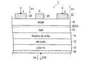
- the typical cross-section figure of the nitride semiconductor element which concerns on embodiment.
- etching is performed in the direction of arrow E, and the vertical leakage current I r V with respect to the total leakage current I r T when the transistor is turned off in a pseudo manner.
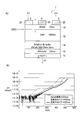
- FIG. 6 is an explanatory diagram of the vertical leakage current I r V and the horizontal leakage current I r H with respect to the total leakage current I r T when the transistor is turned off, and (b) between the total leakage current I r T and the source and drain.
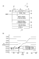
- etching is performed in the direction of arrow E, and the vertical leakage current I r V with respect to the total leakage current I r T when the transistor is turned off in a pseudo manner.
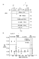
- An explanatory diagram of the lateral leakage current I r H (b) a diagram showing the relationship between the longitudinal leakage current I r V and the lateral leakage current I r H at an applied voltage of 400 V and the etching depth t from the AlGaN layer surface. .
- the typical cross-section figure of the nitride semiconductor device applied to the simulation of an energy band structure is the typical cross-section figure of the nitride semiconductor device applied to the simulation of an energy band structure.
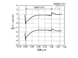
- FIG. 4 is an energy band structure diagram in the vicinity of the GaN buffer layer 16 and the AlGaN buffer layer 28 in a standard state in the nitride semiconductor device according to the embodiment.
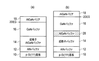
- the energy band structure (STD) in the vicinity of the GaN buffer layer / AlGaN buffer layer in the standard state and the vicinity of the GaN buffer layer / AlGaN buffer layer in a state in which the strain in the AlGaN buffer layer is zero The comparison figure of the energy band structure (A) in FIG. (A) A schematic cross-sectional structure diagram of a nitride semiconductor device according to an embodiment in which tensile stress is introduced into the GaN buffer layer to reduce strain of the AlGaN buffer layer, and (b) corresponds to each layer of FIG. The figure explaining film thickness (nm), Al composition (%), and distortion.
- the energy band structure figure of the nitride semiconductor device which concerns on embodiment which relieve
- the nitride semiconductor device 1 includes a substrate 10, a first buffer layer 12 disposed on the substrate 10, and a second buffer disposed on the first buffer layer 12.
- a layer 14 a third buffer layer 28 made of an AlGaN-based nitride semiconductor disposed on the second buffer layer 14, and a fourth buffer layer 16 made of a GaN-based nitride semiconductor disposed on the third buffer layer 28.
- the gate electrode 26 is disposed.
- the third buffer layer 28 is lattice-relaxed.
- the back electrode 24 is disposed on the back surface side of the substrate 10 opposite to the surface surface on which the first buffer layer 12 is disposed.
- the substrate 10 is made of, for example, p-type silicon (Si) having a plane orientation (111).
- the strain applied to the third buffer layer 28 may be zero or tensile strain.
- the strain applied to the fourth buffer layer 16 may be zero or compressive strain.
- the third buffer layer 28 and the fourth buffer layer 16 may be doped with carbon.
- carbon may be doped at the interface between the third buffer layer 28 and the fourth buffer layer 16.
- the carbon doping level may be, for example, about 1 ⁇ 10 17 to about 1 ⁇ 10 21 (cm ⁇ 3 ).
- the first buffer layer 12 may be made of AlN.
- the second buffer layer 14 may be composed of a superlattice.
- the superlattice is composed of a pair having an AlGaN layer as a quantum well layer and an AlN layer as a barrier layer.
- the thickness of the AlGaN layer / AlN layer is, for example, about 20 nm / about 3 nm.
- the third buffer layer 28 is made of Al x Ga 1-x N having an Al composition x, and x is 10% of y, where y is the average Al composition of the superlattice of the second buffer layer 14. It is desirable that it be smaller.
- the second buffer layer 14 is made of a single AlGaN layer
- the third buffer layer 28 is made of Al x Ga 1-x N with an Al composition x, and the Al compositions are different from each other. Also good.
- the fourth buffer layer 16 may be made of GaN.
- barrier layer 18 may be made of AlGaN.
- the film thickness of the third buffer layer is preferably 100 nm or more.
- the nitride semiconductor device 1 has a HEMT structure transistor configuration.
- the first buffer layer 12 is the AlN buffer layer 12
- the second buffer layer 14 is the AlGaN single layer 14 or the superlattice buffer layer 14
- the third buffer layer 28 is the AlGaN buffer layer 28
- the fourth buffer layer 16 is referred to as a GaN buffer layer 16
- the barrier layer 18 is referred to as an AlGaN barrier layer 18 to clarify the correspondence between each part.
- the vertical leakage current I r V and the horizontal leakage current I r H with respect to the total leakage current I r T are schematically represented as shown in FIG. In FIG. 2, the AlGaN buffer layer 28 is omitted for convenience of explanation.
- a bias voltage is applied between drain electrode 22 and source electrode 20, and between source electrode 20 and ground potential, between drain electrode 22 and ground potential, and between back electrode 24 and ground potential.
- I r T total leakage current I r T
- lateral leakage current I r H lateral leakage current I r H
- longitudinal leakage current I r V longitudinal leakage current
- etching is performed in the direction of arrow E, and the vertical leakage current I r V ⁇ horizontal with respect to the total leakage current I r T when the transistor is turned off in a pseudo manner.
- the direction leakage current I r H is expressed as shown in FIG. 3A, and the total leakage current I r T with the thickness of the AlGaN layer single film 14 or the superlattice buffer layer 14 as a parameter between the source and drain.
- the relationship of the applied voltage V r is expressed as shown in FIG.
- the total leakage current I r T increases the thickness of the second buffer layer 14 as shown in FIG. Then, the tendency for destruction tolerance to increase is seen.
- the leakage current that flows when the transistor is off is small.
- the thickness of the AlN buffer layer 12 is about 200 nm.
- the thickness of the GaN buffer layer 16 is about 1000 nm.
- the thickness of the AlGaN barrier layer 18 is about 25 nm.
- the distance between the source electrode 20 and the drain electrode 22 is about 10 ⁇ m.
- the relationship between the longitudinal leakage current I r V using the thickness of the AlGaN single layer 14 or the superlattice buffer layer 14 as a parameter and the applied voltage V r between the source and drain is This is expressed as shown in FIG.
- the vertical leakage current I r V decreases and the ratio of the horizontal leakage current I r H increases. It has increased.
- the total film thickness is made constant, the film thickness ratio of the GaN buffer layer 16 and the AlGaN buffer layer 28 is changed, etching is performed in the direction of arrow E, and the pseudo transistor
- An explanatory view of the vertical leakage current I r V and the horizontal leakage current I r H with respect to the total leakage current I r T when the OFF state is formed is expressed as shown in FIG.
- the relationship between the leakage current I r T and the applied voltage V r between the source and the drain is expressed as shown in FIG.
- the film thickness of the AlGaN buffer layer 28 is changed.
- the thicker the thickness the smaller the leakage current. That is, there is a high possibility that the total leakage current I r T passes through the GaN buffer layer 16.
- the ratio of the lateral leakage current I r H passing through the GaN buffer layer 16 in the lateral direction increases.
- the thickness of the AlN buffer layer 12 is about 200 nm, for example.
- the thickness of the AlGaN buffer layer 28 is about 400 nm, for example.
- the thickness of the GaN buffer layer 16 is about 1000 nm, for example.
- the thickness of the AlGaN barrier layer 18 is about 25 nm, for example.
- the vertical leakage current I r V (A / cm 2 ) / lateral leakage current I r H (A / cm 2 ) at an applied voltage of 400 V and etching from the surface of the AlGaN barrier layer 18 are performed.
- the relationship with the depth t (nm) is expressed as shown in FIG.
- the main leakage current path is the interface between the GaN buffer layer 16 and the AlGaN buffer layer 28.
- the strain state of AlGaN buffer layer 28 and GaN buffer layer 16 is controlled or C doping is performed, and C at the interface between GaN buffer layer 16 and AlGaN buffer layer 28 is implemented.
- the concentration to be maximum the total leakage current I r T (A / cm 2 ) can be reduced.
- the thickness of the AlN buffer layer 12 is, for example, about 200 nm.
- the thickness of the AlGaN buffer layer 28 formed of the Al 0.12 Ga 0.88 N layer is, for example, about 400 nm.
- the thickness of the GaN buffer layer 16 is about 1000 nm, for example.
- the thickness of the AlGaN barrier layer 18 formed of the Al 0.25 Ga 0.75 N layer is, for example, about 25 nm. 2DEG is formed at the interface between the GaN buffer layer 16 and the AlGaN barrier layer 18.
- the effect of reducing the leakage current by C doping will be described using the simulation result of the energy band structure.
- the GaN buffer layer (16) / AlGaN buffer layer ( 28) Pay attention to the interface.
- the strain state of the GaN buffer layer 16 and the strain state of the AlGaN buffer layer 28 are used as parameters.
- the AlGaN barrier layer 18 formed of the Al 0.25 Ga 0.75 N layer is completely distorted with respect to the GaN buffer layer 16 in the standard state.
- the AlGaN buffer layer 28 formed of the Al 0.12 Ga 0.88 N layer is completely distorted with respect to the AlN buffer layer 12.
- the underlying AlN buffer layer 12 is lattice-relaxed, and the a-axis lattice constant a ( ⁇ ) of the AlGaN buffer layer 28 formed of the Al 0.12 Ga 0.88 N layer is equal to the theoretical value 3.1120 ( ⁇ ) of AlN. .
- the GaN buffer layer 16 is in a tensile strain state where cracks are likely to occur.
- the AlGaN barrier layer 18 formed of the Al 0.25 Ga 0.75 N layer is completely distorted with respect to the GaN buffer layer 16 in a state where the strain in the GaN buffer layer 16 is zero.
- the AlGaN buffer layer 28 formed of the Al 0.12 Ga 0.88 N layer is completely distorted with respect to the AlN buffer layer 12.
- the underlying AlN buffer layer 12 is lattice-relaxed, and the a-axis lattice constant a ( ⁇ ) of the AlGaN buffer layer 28 is equal to the theoretical value 3.1120 ( ⁇ ) of AlN.
- the GaN buffer layer 16 is not distorted, and the a-axis lattice constant a ( ⁇ ) of the AlGaN buffer layer 28 is equal to the theoretical value 3.1891 ( ⁇ ) of GaN.
- the AlGaN barrier layer 18 formed of the Al 0.25 Ga 0.75 N layer is completely distorted with respect to the GaN buffer layer 16 in a state where the strain in the AlGaN buffer layer 28 is zero. Further, the AlGaN buffer layer 28 formed of the Al 0.12 Ga 0.88 N layer is not distorted, and the a-axis lattice constant a ( ⁇ ) of the AlGaN buffer layer 28 is the theoretical value 3.1798 of the Al 0.12 Ga 0.88 N layer. It is equal to ( ⁇ ). On the other hand, the GaN buffer layer 16 is in a tensile strain limit where cracks occur.
- the energy band structure in the vicinity of the GaN buffer layer 16 and the AlGaN buffer layer 28 corresponding to the standard state is expressed as shown in FIG.
- the energy band structure in the vicinity of the GaN buffer layer 16 and the AlGaN buffer layer 28 in a state where the strain of the GaN buffer layer 16 is zero (FIG. 9) is as shown in FIG. expressed.
- the energy band structure in the vicinity of the GaN buffer layer 16 and the AlGaN buffer layer 28 in a state where the strain of the AlGaN buffer layer 28 is zero is expressed as shown in FIG.
- the energy level of the GaN buffer layer 16 in the vicinity of the interface with the AlGaN buffer layer 28 is lower than that at the center of the GaN buffer layer 16 because the tensile strain in the GaN buffer layer 16 is about +0.11 (%). This is due to polarization.
- the spontaneous polarization of the AlGaN buffer layer 28 is negative on the surface side, the energy level increases, but the electric field strength due to tensile strain in the GaN buffer layer 16 is larger.
- carbon (C) is doped into GaN buffer layer 16 and AlGaN buffer layer 28 in order to lower the carrier concentration at the interface between GaN buffer layer 16 and AlGaN buffer layer 28. .
- carbon (C) is doped in a region where the energy level is lower than that of the GaN buffer layer 16 (near the interface with the AlGaN buffer layer 28) by the piezoelectric field.
- the doping level of carbon (C) is, for example, about 1 ⁇ 10 17 (cm ⁇ 3 ) to about 1 ⁇ 10 21 (cm ⁇ 3 ).
- FIG. 14A A schematic cross-sectional structure of the nitride semiconductor device according to the comparative example is represented as shown in FIG. 14A, and a schematic cross-sectional structure of the nitride semiconductor device according to the embodiment is shown in FIG. 14B. It is expressed as follows.
- the lattice of the superlattice buffer layer 14 or the AlGaN layer single film 14 is distorted with respect to the AlN buffer layer 12.
- the superlattice buffer layer 14 or the AlGaN layer single film 14 is subjected to in-plane compressive stress because the a-axis lattice constant a is larger than the AlN buffer layer 12. Since this compressive stress lowers the energy level at the interface between the GaN buffer layer 16 and the superlattice buffer layer 14 or the AlGaN layer single film 14 (piezo effect), it becomes a path of leakage current.
- the GaN buffer layer 16 and the superlattice buffer layer 14 or the AlGaN layer single film 14 In the nitride semiconductor device 1 according to the embodiment, in order to reduce the leakage current passing through the GaN buffer layer 16, the GaN buffer layer 16 and the superlattice buffer layer 14 or the AlGaN layer single film 14 An AlGaN buffer layer 28 having a lattice relaxation is disposed therebetween.
- the energy band structure (STD) in the vicinity of the GaN buffer layer 16 and the AlGaN buffer layer 28 in the standard state and the energy band structure in a state in which the strain in the AlGaN buffer layer 28 is zero ( A comparative diagram of curve A) is represented as shown in FIG. FIG. 15 corresponds to the graph displayed by superimposing FIG. 11 and FIG.
- FIG. 1 A schematic cross-sectional structure of the nitride semiconductor device according to the embodiment in which tensile stress is introduced into the GaN buffer layer 16 to relax the strain of the AlGaN buffer layer 28 is expressed as shown in FIG.
- the state of film thickness (nm), Al composition (%), and strain corresponding to each layer in (a) is expressed as shown in FIG.
- the film thickness of the AlGaN barrier layer 18 is, for example, about 25 nm, and the Al composition x is 25%. Therefore, the AlGaN barrier layer 18 is represented by Al 0.25 Ga 0.75 N. A tensile stress is applied to the AlGaN barrier layer 18.
- the film thickness of the GaN buffer layer 16 is, for example, about 1000 nm. A tensile stress is applied to the GaN buffer layer 16.
- the film thickness of the AlGaN buffer layer 28 is, for example, about 400 nm, and the Al composition x is 12%. Therefore, the AlGaN buffer layer 28 is represented by Al 0.12 Ga 0.88 N. Since neither the tensile stress nor the compressive stress is applied to the AlGaN buffer layer 28, the strain is zero.
- the superlattice buffer layer 14 is formed of 68 pairs of an AlN barrier layer and an AlGaN well layer, and has a film thickness of, for example, about 1700 nm and an average Al composition y of about 24%.
- the superlattice buffer layer 14 has a superlattice pair (film thickness: 20 nm / 5 nm) represented by Al 0.05 Ga 0.95 N / AlN.
- the magnitude relationship between the Al composition x of the AlGaN buffer layer 28 represented by Al x Ga 1-x N and the average Al composition y of the superlattice buffer layer 14 is x ⁇ y.
- x is preferably smaller than y by 0.1 (10%) or more.
- the film thickness of the AlGaN buffer layer 28 represented by Al x Ga 1-x N is preferably about 100 nm or more, for example. The greater the difference between the average Al composition y of the superlattice buffer layer 14 and the Al composition x of the AlGaN buffer layer 28, the easier the AlGaN buffer layer 28 relaxes, and the thicker the AlGaN buffer layer 28, the greater the AlGaN buffer layer 28. This is because the layer 28 is easily lattice-relaxed.
- the energy band structure of the semiconductor element 1 is expressed as shown by the thick line in FIG. In FIG. 17, the solid line corresponds to the energy band structure of FIG. 13 (the energy band structure of curve A of FIG. 15).
- the AlGaN buffer layer 28 has relaxed strain.
- the thermal expansion coefficient of the silicon substrate 10 Expressing (CTE Coefficient of Thermal Expansion)
- CTE Si, AlGaN buffer layer 28 with CTE AlGaN, relationship CTE Si ⁇ CTE AlGaN are satisfied,
- the AlGaN buffer layer 28 is susceptible to tensile stress.
- the relationship between the Al composition x of the Al x Ga 1-x N layer of the nitride semiconductor device 1 according to the embodiment and the a-axis lattice constant a is expressed as shown in FIG.
- the a-axis lattice constant a of AlN is 3.1120
- the a-axis lattice constant a of GaN is 3.11891
- the a-axis lattice constant a of Al 0.12 Ga 0.88 N is 3.1798.
- the nitride semiconductor device of the present invention can be used for all power devices such as a high-frequency power semiconductor module and a high-frequency intelligent power module. Applicable to telephones, digital cameras, video cameras, tablet terminals, electric cars, desktop computers, printers, television receivers, notebook computers, docking stations, home servers, etc., and inverters and converters for solar cells and industrial equipment. is there.
- SYMBOLS 1 Nitride semiconductor element 10 ... Substrate 12 ... 1st buffer layer (AlN buffer layer) 14 ... Second buffer layer (AlGaN layer single layer or superlattice buffer layer) 16 ... Fourth buffer layer (GaN buffer layer) 18 ... Barrier layer (AlGaN barrier layer) 20 ... Source electrode 22 ... Drain electrode 24 ... Back electrode 26 ... Gate electrode 28 ... Third buffer layer (AlGaN buffer layer) 2DEG ... 2-dimensional electron gas I r ... leakage current V r ... applied voltage I r T ... total leakage current I r V ... longitudinal leakage current I r H ... lateral leakage current D1, D2, D3, D4 ... thickness t ... depth from the surface
Landscapes
- Junction Field-Effect Transistors (AREA)
- Chemical & Material Sciences (AREA)
- Engineering & Computer Science (AREA)
- Materials Engineering (AREA)
Abstract
窒化物半導体素子(1)は、基板(10)と、基板上に配置された第1バッファ層(12)と、第1バッファ層上に配置された第2バッファ層(14)と、第2バッファ層上に配置されたAlGaN系窒化物半導体からなる第3バッファ層(28)と、第3バッファ層上に配置されたGaN系窒化物半導体からなる第4バッファ層(16)と、第4バッファ層上に配置されたAlGaN系窒化物半導体からなるバリア層(18)と、バリア層上に配置されたソース電極(20)、ドレイン電極(22)およびソース電極およびドレイン電極の間に配置されたゲート電極(26)とを備え、第3バッファ層は格子緩和されている。リーク電流を抑制し、破壊耐量を向上した窒化物半導体素子を提供する。
Description
本発明は、窒化物半導体素子に関し、特にリーク電流を抑制し、破壊耐量を向上した窒化物半導体素子に関する。
高電子移動度トランジスタ(HEMT:High Electron Mobility Transistor)構造を有する窒化物半導体素子において、炭素(C)などの不純物ドーピングを実施してリーク電流を抑制する技術は、各種提案されている(例えば、特許文献1および特許文献2参照。)。
GaN電子走行層の厚さを広い範囲で選択することができ、デバイス設計の自由度を高めることができる窒化物半導体素子、および耐圧および信頼性に優れる窒化物半導体素子パッケージについても開示されている(例えば、特許文献3参照。)。
本発明の目的は、リーク電流を抑制し、破壊耐量を向上した窒化物半導体素子を提供することにある。
上記目的を達成するための本発明の一態様によれば、基板と、前記基板上に配置された第1バッファ層と、記第1バッファ層上に配置された第2バッファ層と、前記第2バッファ層上に配置されたAlGaN系窒化物半導体からなる第3バッファ層と、前記第3バッファ層上に配置されたGaN系窒化物半導体からなる第4バッファ層と、前記第4バッファ層上に配置されたAlGaN系窒化物半導体からなるバリア層と、前記バリア層上に配置されたソース電極、ドレイン電極および前記ソース電極および前記ドレイン電極の間に配置されたゲート電極とを備え、前記第3バッファ層は格子緩和されている窒化物半導体素子が提供される。
本発明によれば、リーク電流を抑制し、破壊耐量を向上した窒化物半導体素子を提供することができる。
次に、図面を参照して、実施の形態を説明する。以下の図面の記載において、同一又は類似の部分には同一又は類似の符号を付している。ただし、図面は模式的なものであり、厚みと平面寸法との関係、各層の厚みの比率等は現実のものとは異なることに留意すべきである。したがって、具体的な厚みや寸法は以下の説明を参酌して判断すべきものである。又、図面相互間においても互いの寸法の関係や比率が異なる部分が含まれていることはもちろんである。
又、以下に示す実施の形態は、この発明の技術的思想を具体化するための装置や方法を例示するものであって、この発明の実施の形態は、構成部品の材質、形状、構造、配置等を下記のものに特定するものでない。この発明の実施の形態は、特許請求の範囲において、種々の変更を加えることができる。
実施の形態に係る窒化物半導体素子1は、図1に示すように、基板10と、基板10上に配置された第1バッファ層12と、第1バッファ層12上に配置された第2バッファ層14と、第2バッファ層14上に配置されたAlGaN系窒化物半導体からなる第3バッファ層28と、第3バッファ層28上に配置されたGaN系窒化物半導体からなる第4バッファ層16と、第4バッファ層16上に配置されたAlGaN系窒化物半導体からなるバリア層18と、バリア層18上に配置されたソース電極20、ドレイン電極22およびソース電極20およびドレイン電極22の間に配置されたゲート電極26とを備える。ここで、第3バッファ層28は格子緩和されている。
また、基板10の第1バッファ層12が配置される表面側とは反対側の裏面側には、裏面電極24が配置される。
基板10は、例えば、面方位(111)のp型シリコン(Si)から構成される。
また、実施の形態に係る窒化物半導体素子1において、第3バッファ層28に加わる歪みはゼロもしくは引張り歪みであっても良い。
また、実施の形態に係る窒化物半導体素子1において、第4バッファ層16に加わる歪みはゼロもしくは圧縮歪みであっても良い。
また、実施の形態に係る窒化物半導体素子1において、第3バッファ層28と第4バッファ層16に炭素がドーピングされていても良い。
また、特に、第3バッファ層28と第4バッファ層16との界面に炭素がドーピングされていても良い。
また、炭素のドーピングレベルは、例えば、約1×10¹⁷以上約1×10²¹(cm-3)以下であっても良い。
第1バッファ層12は、AlNから構成されていても良い。
第2バッファ層14は、超格子から構成されていても良い。ここで、超格子は、AlGaN層を量子井戸層、AlN層をバリア層とするペアから構成される。AlGaN層/AlN層の厚さは、例えば、約20nm/約3nmである。
また、第3バッファ層28は、Al組成をxとするAlxGa1-xNからなり、第2バッファ層14の超格子の平均Al組成をyとすると、xは、yよりも10%以上小さいことが望ましい。
また、第2バッファ層14は、AlGaN層単膜からなり、第3バッファ層28は、Al組成をxとするAlxGa1-xNからなり、互いにAl組成が異なるように構成されていても良い。
また、第4バッファ層16は、GaNから構成されていても良い。
また、バリア層18は、AlGaNから構成されていても良い。
また、第3バッファ層の膜厚は、100nm以上であることが望ましい。
第4バッファ層16のバリア層18との界面には、2次元電子ガス(2DEG:Two Dimensional Electron Gas)が形成される。AlGaNからなるバリア層18は、この2DEGに対する電子供給層としての役割を有し、GaNからなる第4バッファ層16は、電子走行層としての役割を有する。結果として、実施の形態に係る窒化物半導体素子1は、HEMT構造のトランジスタ構成を有する。
以下の説明においては、第1バッファ層12をAlNバッファ層12、第2バッファ層14をAlGaN層単膜14若しくは超格子バッファ層14、第3バッファ層28をAlGaNバッファ層28、第4バッファ層16をGaNバッファ層16、バリア層18をAlGaNバリア層18と記載し、各部の対応関係を明瞭化する。
実施の形態に係る窒化物半導体素子1において、全リーク電流IrTに対する縦方向リーク電流IrV・横方向リーク電流IrHは、図2に示すように模式的に表される。図2において、AlGaNバッファ層28は説明の都合上、図示を省略している。実施の形態に係る窒化物半導体素子1において、ドレイン電極22・ソース電極20間にバイアス電圧を印加し、ソース電極20と接地電位間・ドレイン電極22と接地電位間・裏面電極24と接地電位間に導通する電流をそれぞれ、全リーク電流IrT・横方向リーク電流IrH・縦方向リーク電流IrVとして検出する。
実施の形態に係る窒化物半導体素子1において、矢印E方向にエッチングを実施して、擬似的にトランジスタのオフ状態を形成した場合の全リーク電流IrTに対する縦方向リーク電流IrV・横方向リーク電流IrHは、図3(a)に示すように表され、AlGaN層単膜14若しくは超格子バッファ層14の厚さをパラメータとする全リーク電流IrTとソース・ドレイン間の印加電圧Vrの関係は、図3(b)に示すように表される。
ここで、AlGaN層単膜14若しくは超格子バッファ層14の厚さをパラメータとすると、図3(b)に示すように、全リーク電流IrTは、第2バッファ層14の厚さを厚くすると、破壊耐量が増大する傾向が見られる。
実施の形態に係る窒化物半導体素子1において、トランジスタがオフのときに流れるリーク電流は、少ない方が望ましい。
超格子バッファ層14の超格子のペア数を増やす(総膜厚を増やす)と全リーク電流IrT(縦方向リーク電流IrV)は減少し、破壊電圧も改善する。
ここで、AlNバッファ層12の厚さは約200nmである。AlGaN層単膜14の厚さは、約200nmであり、AlGaN/AlN=20nm/3nmからなる超格子バッファ層14の厚さは、ペア数20の場合、460nm、ペア数40の場合、920nmである。GaNバッファ層16の厚さは約1000nmである。AlGaNバリア層18の厚さは約25nmである。また、ソース電極20とドレイン電極22の間隔は、約10μmである。
実施の形態に係る窒化物半導体素子1において、AlGaN層単膜14若しくは超格子バッファ層14の厚さをパラメータとする縦方向リーク電流IrVとソース・ドレイン間の印加電圧Vrの関係は、図4(a)に示すように表される。
また、実施の形態に係る窒化物半導体素子1において、ソース・ドレイン間の印加電圧Vr=400Vにおける垂直成分の割合は、図4(b)に示すように表される。すなわち、AlGaN層単膜14では、全リーク電流IrT=9.2(A/cm2)、縦方向リーク電流IrV=7.9(A/cm2)であり、垂直成分の割合は、86.1%である。超格子バッファ層14でペア数20の場合では、全リーク電流IrT=5.6×10-1(A/cm2)、縦方向リーク電流IrV=3.9×10-1(A/cm2)であり、垂直成分の割合は、69.4%である。さらに、超格子バッファ層14でペア数40の場合では、全リーク電流IrT=2.2×10-1(A/cm2)、縦方向リーク電流IrV=6.1×10-2(A/cm2)であり、垂直成分の割合は、28.24%である。
図4(a)および図4(b)から明らかなように、AlGaN層単膜14・超格子バッファ層14の厚さを増やすと、縦方向リーク電流IrVは減少し、破壊電圧も改善している。
一方、横方向リーク電流IrH(=IrT-IrV)の割合は、AlGaN層単膜では、13.9%、超格子のペア数20の場合では、30.6%、さらに、超格子のペア数40の場合では、71.8%である。図4(a)および図4(b)から明らかなように、超格子バッファ層14のペア数を増やすと、縦方向リーク電流IrVは減少し、横方向リーク電流IrHの割合が増加している。
すなわち、AlGaN層単膜14若しくは超格子バッファ層14の膜厚を増やすことで縦方向の電気抵抗が大きくなり、全リーク電流IrTの内、GaNバッファ層16を横方向に経由する横方向リーク電流IrHの割合が増加している。
実施の形態に係る窒化物半導体素子1において、総膜厚を一定にして、GaNバッファ層16とAlGaNバッファ層28の膜厚比を変え、矢印E方向にエッチングを実施して、擬似的にトランジスタのオフ状態を形成した場合の全リーク電流IrTに対する縦方向リーク電流IrV・横方向リーク電流IrHの説明図は、図5(a)に示すように表される。図5(a)においては、GaNバッファ層16の厚さを、厚さD1=1000nmと厚さD2=200nmの2通りに変化させており、第3バッファ層28の厚さを、厚さD3=200nmと厚さD4=1000nmの2通りに変化させている。
実施の形態に係る窒化物半導体素子1において、総膜厚を一定にして、AlGaNバッファ層28の厚さを、厚さD3=200nmと厚さD4=1000nmの2通りに変化させた場合の全リーク電流IrTとソース・ドレイン間の印加電圧Vrの関係は、図5(b)に示すように表される。AlGaN層単膜:200nmの曲線は、AlGaNバッファ層28の厚さD3=200nm、GaNバッファ層16の厚さD1=1000nmに対応し、AlGaN層単膜:1000nmの曲線は、AlGaNバッファ層28の厚さD3=1000nm、GaNバッファ層16の厚さD2=200nmに対応する。
図5(a)および図5(b)から明らかなように、総膜厚を一定にして、GaNバッファ層16とAlGaNバッファ層28の膜厚比を変えたとき、AlGaNバッファ層28の膜厚の厚い方が、リーク電流が少なくなる。すなわち、全リーク電流IrTは、GaNバッファ層16を経由している可能性が高い。全リーク電流IrTの内、GaNバッファ層16を横方向に経由する横方向リーク電流IrHの割合が増加している。
実施の形態に係る窒化物半導体素子において、矢印E方向にエッチングを実施して、擬似的にトランジスタのオフ状態を形成した場合の全リーク電流IrTに対する縦方向リーク電流IrV・横方向リーク電流IrHの説明図は、図6(a)に示すように表される。図6(a)において、AlNバッファ層12の厚さは、例えば、約200nmである。超格子(AlGaN/AlN=20nm/3nm)で形成される超格子バッファ層14の厚さは、例えば、約1700nmである。AlGaNバッファ層28の厚さは、例えば、約400nmである。GaNバッファ層16の厚さは、例えば、約1000nmである。AlGaNバリア層18の厚さは、例えば、約25nmである。
図6(a)の構成において、印加電圧400Vにおける縦方向リーク電流IrV(A/cm2)・横方向リーク電流IrH(A/cm2)とAlGaNバリア層18の表面からのエッチング深さt(nm)との関係は、図6(b)に示すように表される。
図6(b)に示すように、GaNバッファ層16を全てエッチングすると急激に、横方向リーク電流IrH(A/cm2)の値が低下する。このため、GaNバッファ層16とAlGaNバッファ層28の界面にリーク経路が存在していることがわかる。
実施の形態に係る窒化物半導体素子1において、主なリーク電流経路はGaNバッファ層16とAlGaNバッファ層28の界面である。
ここで、AlGaNバッファ層28には、圧縮応力が加わっている。このため、AlGaNバッファ層28にピエゾ電界が発生し、GaNバッファ層16との界面においてエネルギー準位が下がるため、リーク電流経路が形成される。
実施の形態に係る窒化物半導体素子1においては、AlGaNバッファ層28およびGaNバッファ層16の歪み状態を制御、若しくはCドープを実施して、かつGaNバッファ層16とAlGaNバッファ層28の界面のC濃度が最大になるように制御することによって、全リーク電流IrT(A/cm2)を低減化可能である。
(エネルギーバンド構造のシミュレーション)
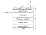
実施の形態に係る窒化物半導体素子1において、エネルギーバンド構造のシミュレーションに適用する模式的断面構造は、図7に示すように表される。
実施の形態に係る窒化物半導体素子1において、エネルギーバンド構造のシミュレーションに適用する模式的断面構造は、図7に示すように表される。
図7において、AlNバッファ層12の厚さは、例えば、約200nmである。超格子(AlGaN/AlN=20nm/3nm)で形成される超格子バッファ層14の厚さは、例えば、約1700nmである。Al0.12Ga0.88N層で形成されるAlGaNバッファ層28の厚さは、例えば、約400nmである。GaNバッファ層16の厚さは、例えば、約1000nmである。Al0.25Ga0.75N層で形成されるAlGaNバリア層18の厚さは、例えば、約25nmである。GaNバッファ層16とAlGaNバリア層18との界面には、2DEGが形成される。
実施の形態に係る窒化物半導体素子1において、Cドープによるリーク電流の低減効果をエネルギーバンド構造のシミュレーション結果を用いて説明する。
Al0.25Ga0.75N層で形成されるAlGaNバリア層18の最表面からAl0.12Ga0.88N層で形成されるAlGaNバッファ層28までのバンド構造において、特にGaNバッファ層(16)/AlGaNバッファ層(28)界面に注目する。また、GaNバッファ層16の歪み状態、およびAlGaNバッファ層28の歪み状態をパラメータとする。
超格子(AlGaN/AlN=20nm/3nm)で形成される超格子バッファ層14・AlNバッファ層12は、ここでは絶縁体として取り扱う。
超格子(AlGaN/AlN=20nm/3nm)で形成される超格子バッファ層14・AlNバッファ層12は、ここでは絶縁体として取り扱う。
(標準状態)
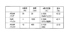
実施の形態に係る窒化物半導体素子1において、標準状態におけるAlGaNバリア層18・GaNバッファ層16・AlGaNバッファ層28のAl組成(%)・膜厚(nm)・a軸格子定数a(Å)・歪み(%)の数値例は、図8に示すように表される。ここで、標準状態とは、AlGaNバッファ層28やGaNバッファ層16に歪み制御を実施していない状態に対応する。
実施の形態に係る窒化物半導体素子1において、標準状態におけるAlGaNバリア層18・GaNバッファ層16・AlGaNバッファ層28のAl組成(%)・膜厚(nm)・a軸格子定数a(Å)・歪み(%)の数値例は、図8に示すように表される。ここで、標準状態とは、AlGaNバッファ層28やGaNバッファ層16に歪み制御を実施していない状態に対応する。
図8に示すように、標準状態において、Al0.25Ga0.75N層で形成されるAlGaNバリア層18は、GaNバッファ層16に対して完全に歪んでいる。また、Al0.12Ga0.88N層で形成されるAlGaNバッファ層28は、AlNバッファ層12に対して完全に歪んでいる。下地のAlNバッファ層12は格子緩和しており、Al0.12Ga0.88N層で形成されるAlGaNバッファ層28のa軸格子定数a(Å)は、AlNの理論値3.1120(Å)に等しい。また、GaNバッファ層16はクラックが発生する限界の引っ張り歪み状態にある。
(GaNバッファ層における歪みゼロ)
また、実施の形態に係る窒化物半導体素子1において、GaNバッファ層16における歪みをゼロとした状態におけるAlGaNバリア層18・GaNバッファ層16・AlGaNバッファ層28のAl組成(%)・膜厚(nm)・a軸格子定数a(Å)・歪み(%)の数値例は、図9に示すように表される。
また、実施の形態に係る窒化物半導体素子1において、GaNバッファ層16における歪みをゼロとした状態におけるAlGaNバリア層18・GaNバッファ層16・AlGaNバッファ層28のAl組成(%)・膜厚(nm)・a軸格子定数a(Å)・歪み(%)の数値例は、図9に示すように表される。
図9に示すように、GaNバッファ層16における歪みをゼロとした状態において、Al0.25Ga0.75N層で形成されるAlGaNバリア層18は、GaNバッファ層16に対して完全に歪んでいる。また、Al0.12Ga0.88N層で形成されるAlGaNバッファ層28は、AlNバッファ層12に対して完全に歪んでいる。下地のAlNバッファ層12は格子緩和しており、AlGaNバッファ層28のa軸格子定数a(Å)は、AlNの理論値3.1120(Å)に等しい。一方、GaNバッファ層16は歪んでおらず、AlGaNバッファ層28のa軸格子定数a(Å)は、GaNの理論値3.1891(Å)に等しい。
(AlGaNバッファ層における歪みゼロ)
また、実施の形態に係る窒化物半導体素子1において、AlGaNバッファ層28における歪みをゼロとした状態におけるAlGaNバリア層18・GaNバッファ層16・AlGaNバッファ層28のAl組成(%)・膜厚(nm)・a軸格子定数a(Å)・歪み(%)の数値例は、図10に示すように表される。
また、実施の形態に係る窒化物半導体素子1において、AlGaNバッファ層28における歪みをゼロとした状態におけるAlGaNバリア層18・GaNバッファ層16・AlGaNバッファ層28のAl組成(%)・膜厚(nm)・a軸格子定数a(Å)・歪み(%)の数値例は、図10に示すように表される。
図10に示すように、AlGaNバッファ層28における歪みをゼロとした状態において、Al0.25Ga0.75N層で形成されるAlGaNバリア層18は、GaNバッファ層16に対して完全に歪んでいる。また、Al0.12Ga0.88N層で形成されるAlGaNバッファ層28は、歪んでおらず、AlGaNバッファ層28のa軸格子定数a(Å)は、Al0.12Ga0.88N層の理論値3.1798(Å)に等しい。一方、GaNバッファ層16はクラックが発生する限界の引っ張り歪み状態にある。
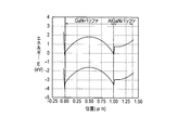
実施の形態に係る窒化物半導体素子1において、標準状態(図8)に対応するGaNバッファ層16・AlGaNバッファ層28近傍におけるエネルギーバンド構造は、図11に示すように表される。
標準状態においては、GaNバッファ層16とAlGaNバッファ層28の界面で、電子が走行しやすい領域が発生している。
また、GaNバッファ層16に引張り歪み、AlGaNバッファ層28に圧縮歪みが発生しているため、ピエゾ電界が発生してGaNバッファ層16とAlGaNバッファ層28の界面のエネルギー準位が下がっている。
GaNバッファ層16のAlGaNバリア層18との界面の2DEGを導通する電流がオフされているとき、AlGaNバリア層18からGaNバッファ層16に供給される電子は、本来、GaNバッファ層16の障壁を乗り越え難いが、GaNバッファ層16中にはリークパスとなり得る、例えば螺旋転位のような転位が分布しているため、この螺旋転位を経由してGaNバッファ層16/AlGaNバッファ層28界面に到達した電子は、リーク電流に寄与する。
実施の形態に係る窒化物半導体素子1において、GaNバッファ層16の歪みをゼロとした状態(図9)におけるGaNバッファ層16・AlGaNバッファ層28近傍におけるエネルギーバンド構造は、図12に示すように表される。
GaNバッファ層16における歪みをゼロとした状態においても、標準状態と同様に、GaNバッファ層16とAlGaNバッファ層28の界面で、電子が走行しやすい領域が発生している。
また、GaNバッファ層16の歪みをゼロとした状態においても、AlGaNバッファ層28に圧縮歪みが発生しているため、ピエゾ電界が発生してGaNバッファ層16とAlGaNバッファ層28の界面のエネルギー準位が下がっている。GaNバッファ層16の歪みをゼロとした状態におけるエネルギーバンド構造(図12)と、標準状態におけるエネルギーバンド構造(図11)とを比較すると、標準状態におけるGaNバッファ層16の歪みが0.11%と小さいため(ただしクラックは発生する)、分極の大きさに変化は見られない。
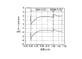
実施の形態に係る窒化物半導体素子1において、AlGaNバッファ層28の歪みをゼロとした状態におけるGaNバッファ層16・AlGaNバッファ層28近傍におけるエネルギーバンド構造は、図13に示すように表される。
AlGaNバッファ層28の歪みをゼロとした状態においては、GaNバッファ層16に引張り歪みが発生しているが、GaNバッファ層16とAlGaNバッファ層28の界面のエネルギー準位が下がる現象は緩和されている。AlGaNバッファ層28の歪みをゼロにすることで、ピエゾ電界が小さくなり、界面のエネルギー準位が上昇している。
GaNバッファ層16の中央部と比べて、AlGaNバッファ層28との界面近傍のGaNバッファ層16のエネルギー準位が低いのは、GaNバッファ層16中の引張り歪み約+0.11(%)と自発分極が原因である。
AlGaNバッファ層28の自発分極は表面側がマイナスなので、エネルギー準位は上がる方向であるが、GaNバッファ層16中の引張り歪みに起因する電界強度の方が大きい。
実施の形態に係る窒化物半導体素子1においては、GaNバッファ層16とAlGaNバッファ層28の界面のキャリア濃度を下げるために、GaNバッファ層16およびAlGaNバッファ層28に炭素(C)がドーピングされる。特に、ピエゾ電界によってエネルギー準位がGaNバッファ層16よりも下がっている領域(AlGaNバッファ層28との界面付近)に炭素(C)がドーピングされることが効果的である。尚、炭素(C)のドーピングレベルは、例えば、約1×10¹⁷(cm-3)~約1×10²¹(cm-3)である。
比較例に係る窒化物半導体素子の模式的断面構造は、図14(a)に示すように表され、実施の形態に係る窒化物半導体素子の模式的断面構造は、図14(b)に示すように表される。
比較例に係る窒化物半導体素子において、超格子バッファ層14若しくはAlGaN層単膜14は、AlNバッファ層12に対して格子が歪んでいる。図14(a)に示すように、超格子バッファ層14若しくはAlGaN層単膜14は、a軸格子定数aがAlNバッファ層12より大きいため、面内に圧縮応力を受ける。この圧縮応力はGaNバッファ層16と超格子バッファ層14若しくはAlGaN層単膜14界面のエネルギー準位を下げるため(ピエゾ効果)、リーク電流の経路となる。
実施の形態に係る窒化物半導体素子1においては、HEMT構造において、GaNバッファ層16を経由するリーク電流を低減するために、GaNバッファ層16と超格子バッファ層14若しくはAlGaN層単膜14との間に、格子緩和したAlGaNバッファ層28を配置している。
実施の形態に係る窒化物半導体素子1において、標準状態におけるGaNバッファ層16・AlGaNバッファ層28近傍におけるエネルギーバンド構造(STD)と、AlGaNバッファ層28における歪みをゼロとした状態におけるエネルギーバンド構造(曲線A)の比較図は、図15に示すように表される。図15は、図11と図13を重ね合わせて表示したグラフに対応する。
標準状態においては、GaNバッファ層16とAlGaNバッファ層28の界面で、電子が走行しやすい領域が発生している。また、GaNバッファ層16に引張り歪み、AlGaNバッファ層28に圧縮歪みが発生しているため、ピエゾ電界が発生してGaNバッファ層16とAlGaNバッファ層28の界面のエネルギー準位が下がる。
AlGaNバッファ層28における歪みをゼロとした状態においては、曲線Aに示すように、GaNバッファ層16に引張り歪みが発生しているが、GaNバッファ層16とAlGaNバッファ層28の界面のエネルギー準位が下がる現象は緩和される。AlGaNバッファ層28の歪みをゼロにすることで、ピエゾ電界が小さくなり、界面のエネルギー準位が上昇する。GaNバッファ層16中の引張り歪み約+0.11(%) が原因でGaNバッファ層16の中央部と比べて、AlGaNバッファ層28との界面近傍のGaNバッファ層16のエネルギー準位が低い。
GaNバッファ層16に引っ張り応力を導入してAlGaNバッファ層28の歪みを緩和した実施の形態に係る窒化物半導体素子の模式的断面構造は、図16(a)に示すように表され、図16(a)の各層に対応する膜厚(nm)・Al組成(%)・歪みの状態は、図16(b)に示すように表される。
AlGaNバリア層18の膜厚は、例えば、約25nmであり、Al組成xは25%である。したがって、AlGaNバリア層18は、Al0.25Ga0.75Nで表される。AlGaNバリア層18には、引っ張り応力が加わる。
GaNバッファ層16の膜厚は、例えば、約1000nmである。GaNバッファ層16には、引っ張り応力が加わる。
AlGaNバッファ層28の膜厚は、例えば、約400nmであり、Al組成xは12%である。したがって、AlGaNバッファ層28は、Al0.12Ga0.88Nで表される。AlGaNバッファ層28には、引っ張り応力・圧縮応力のいずれも加わっていないため、歪みゼロである。
超格子バッファ層14は、AlN障壁層とAlGaNウェル層の68ペアで形成され、膜厚は、例えば、約1700nmであり、平均Al組成yは、約24%である。超格子バッファ層14は、Al0.05Ga0.95N/AlNで表される超格子ペア(膜厚20nm/5nm)を有する。
AlxGa1-xNで表されるAlGaNバッファ層28のAl組成xと超格子バッファ層14の平均Al組成yの大小関係は、x<yである。ここで、xは、yよりも0.1(10%)以上小さいことが望ましい。また、AlxGa1-xNで表されるAlGaNバッファ層28の膜厚は、例えば、約100nm以上であることが望ましい。超格子バッファ層14の平均Al組成yとAlGaNバッファ層28のAl組成xに差があるほど、AlGaNバッファ層28は格子緩和しやすく、また、AlGaNバッファ層28の膜厚が厚いほど、AlGaNバッファ層28は格子緩和しやすいからである。
AlGaNバッファ層28の歪みを緩和して、さらにGaNバッファ層16に圧縮歪みを導入した(ピエゾ電界が発生してAlGaNバッファ層28との界面エネルギー準位が上がる)、実施の形態に係る窒化物半導体素子1のエネルギーバンド構造は、図17の太線に示すように表される。尚、図17において、実線は、図13のエネルギーバンド構造(図15の曲線Aのエネルギーバンド構造)に対応している。
AlGaNバッファ層28は歪みが緩和している。ここで、シリコン基板10の熱膨張係数(CTE:Coefficient of Thermal Expansion)をCTESi、AlGaNバッファ層28の熱膨張係数をCTEAlGaNで表すと、CTESi<CTEAlGaNの関係が成立しており、AlGaNバッファ層28は引張り応力を受けやすくなっている。
AlGaNバッファ層28の歪みを緩和し、さらに引張り応力を導入することで、GaNバッファ層16)/AlGaNバッファ層28界面でのポテンシャルの落ち込みを無くしたポテンシャル構造を実現可能である。
実施の形態に係る窒化物半導体素子1のAlxGa1-xN層のAl組成xとa軸格子定数aの関係を示すは、図18に示すように表される。例えば、AlNのa軸格子定数aは3.1120、GaNのa軸格子定数aは3.1891、Al0.12Ga0.88Nのa軸格子定数aは3.1798である。
以上説明したように、本実施の形態によれば、リーク電流を抑制し、破壊耐量を向上した窒化物半導体素子を提供することができる。
[その他の実施の形態]
上記のように、実施の形態によって記載したが、この開示の一部をなす論述および図面は例示的なものであり、この発明を限定するものであると理解すべきではない。この開示から当業者には様々な代替実施の形態、実施例および運用技術が明らかとなろう。
上記のように、実施の形態によって記載したが、この開示の一部をなす論述および図面は例示的なものであり、この発明を限定するものであると理解すべきではない。この開示から当業者には様々な代替実施の形態、実施例および運用技術が明らかとなろう。
このように、本発明はここでは記載していない様々な実施の形態などを含む。
本発明の窒化物半導体素子は、高周波パワー半導体モジュール、高周波インテリジェントパワーモジュールなどパワーデバイス全般に利用可能であり、特に、高周波・小型・軽量化が求められている分野として、ワイヤレス受給電装置、携帯電話、デジタルカメラ、ビデオカメラ、タブレット端末、電気自動車、デスクトップコンピュータ、プリンタ、テレビ受像機、ノートブックコンピュータ、ドッキングステーション、ホームサーバなど、また太陽電池・産業機器向けのインバータ、コンバータなどに適用可能である。
1…窒化物半導体素子
10…基板
12…第1バッファ層(AlNバッファ層)
14…第2バッファ層(AlGaN層単膜若しくは超格子バッファ層)
16…第4バッファ層(GaNバッファ層)
18…バリア層(AlGaNバリア層)
20…ソース電極
22…ドレイン電極
24…裏面電極
26…ゲート電極
28…第3バッファ層(AlGaNバッファ層)
2DEG…2次元電子ガス
Ir…リーク電流
Vr…印加電圧
IrT…全リーク電流
IrV…縦方向リーク電流
IrH…横方向リーク電流
D1、D2、D3、D4…厚さ
t…表面からの深さ
10…基板
12…第1バッファ層(AlNバッファ層)
14…第2バッファ層(AlGaN層単膜若しくは超格子バッファ層)
16…第4バッファ層(GaNバッファ層)
18…バリア層(AlGaNバリア層)
20…ソース電極
22…ドレイン電極
24…裏面電極
26…ゲート電極
28…第3バッファ層(AlGaNバッファ層)
2DEG…2次元電子ガス
Ir…リーク電流
Vr…印加電圧
IrT…全リーク電流
IrV…縦方向リーク電流
IrH…横方向リーク電流
D1、D2、D3、D4…厚さ
t…表面からの深さ
Claims (14)
- 基板と、
前記基板上に配置された第1バッファ層と、
前記第1バッファ層上に配置された第2バッファ層と、
前記第2バッファ層上に配置されたAlGaN系窒化物半導体からなる第3バッファ層と、
前記第3バッファ層上に配置されたGaN系窒化物半導体からなる第4バッファ層と、
前記第4バッファ層上に配置されたAlGaN系窒化物半導体からなるバリア層と、
前記バリア層上に配置されたソース電極、ドレイン電極および前記ソース電極および前記ドレイン電極の間に配置されたゲート電極と
を備え、前記第3バッファ層は格子緩和されていることを特徴とする窒化物半導体素子。 - 前記第3バッファ層に加わる歪みはゼロもしくは引張り歪みであることを特徴とする請求項1に記載の窒化物半導体素子。
- 前記第4バッファ層に加わる歪みはゼロもしくは圧縮歪みであることを特徴とする請求項1または2に記載の窒化物半導体素子。
- 前記第3バッファ層と前記第4バッファ層に炭素がドーピングされていることを特徴とする請求項1~3のいずれか1項に記載の窒化物半導体素子。
- 前記第3バッファ層と前記第4バッファ層との界面に炭素がドーピングされていることを特徴とする請求項1~3のいずれか1項に記載の窒化物半導体素子。
- 前記炭素のドーピングレベルは、1×10¹⁷以上1×10²¹(cm-3)以下であることを特徴とする請求項4または5に記載の窒化物半導体素子。
- 前記第1バッファ層は、AlNからなることを特徴とする請求項1~6のいずれか1項に記載の窒化物半導体素子。
- 前記第2バッファ層は、超格子からなることを特徴とする請求項1~7のいずれか1項に記載の窒化物半導体素子。
- 前記超格子は、AlGaN層とAlN層のペアからなることを特徴とする請求項8に記載の窒化物半導体素子。
- 前記第3バッファ層は、Al組成をxとするAlxGa1-xNからなり、前記超格子の平均Al組成をyとすると、xは、yよりも10%以上小さいことを特徴とする請求項9に記載の窒化物半導体素子。
- 前記第2バッファ層は、AlGaN層単膜からなり、前記第3バッファ層は、Al組成をxとするAlxGa1-xNからなり、互いにAl組成が異なることを特徴とする請求項1~7のいずれか1項に記載の窒化物半導体素子。
- 前記第4バッファ層は、GaNからなることを特徴とする請求項1~11のいずれか1項に記載の窒化物半導体素子。
- 前記第3バッファ層の膜厚は、100nm以上であることを特徴とする請求項1~12のいずれか1項に記載の窒化物半導体素子。
- 前記基板は、(111)面の面方位を有するp型Siからなることを特徴とする請求項1~13のいずれか1項に記載の窒化物半導体素子。
Priority Applications (1)
| Application Number | Priority Date | Filing Date | Title |
|---|---|---|---|
| US14/935,343 US20160064488A1 (en) | 2013-05-09 | 2015-11-06 | Nitride based semiconductor device |
Applications Claiming Priority (2)
| Application Number | Priority Date | Filing Date | Title |
|---|---|---|---|
| JP2013-099233 | 2013-05-09 | ||
| JP2013099233A JP2014220407A (ja) | 2013-05-09 | 2013-05-09 | 窒化物半導体素子 |
Related Child Applications (1)
| Application Number | Title | Priority Date | Filing Date |
|---|---|---|---|
| US14/935,343 Continuation US20160064488A1 (en) | 2013-05-09 | 2015-11-06 | Nitride based semiconductor device |
Publications (1)
| Publication Number | Publication Date |
|---|---|
| WO2014181856A1 true WO2014181856A1 (ja) | 2014-11-13 |
Family
ID=51867328
Family Applications (1)
| Application Number | Title | Priority Date | Filing Date |
|---|---|---|---|
| PCT/JP2014/062437 Ceased WO2014181856A1 (ja) | 2013-05-09 | 2014-05-09 | 窒化物半導体素子 |
Country Status (3)
| Country | Link |
|---|---|
| US (1) | US20160064488A1 (ja) |
| JP (1) | JP2014220407A (ja) |
| WO (1) | WO2014181856A1 (ja) |
Families Citing this family (12)
| Publication number | Priority date | Publication date | Assignee | Title |
|---|---|---|---|---|
| JP5781292B2 (ja) * | 2010-11-16 | 2015-09-16 | ローム株式会社 | 窒化物半導体素子および窒化物半導体パッケージ |
| TWI703726B (zh) * | 2016-09-19 | 2020-09-01 | 新世紀光電股份有限公司 | 含氮半導體元件 |
| US10886408B2 (en) * | 2016-09-29 | 2021-01-05 | Intel Corporation | Group III-V material transistors employing nitride-based dopant diffusion barrier layer |
| TWI701715B (zh) * | 2017-06-06 | 2020-08-11 | 黃知澍 | N-face III族/氮化物磊晶結構及其主動元件與其積體化之極性反轉製作方法 |
| TWI678723B (zh) * | 2018-10-26 | 2019-12-01 | 世界先進積體電路股份有限公司 | 高電子遷移率電晶體裝置及其製造方法 |
| US11515407B2 (en) * | 2018-12-26 | 2022-11-29 | Intel Corporation | High breakdown voltage structure for high performance GaN-based HEMT and MOS devices to enable GaN C-MOS |
| JP7448314B2 (ja) * | 2019-04-19 | 2024-03-12 | 株式会社東芝 | 半導体装置 |
| WO2021243653A1 (zh) * | 2020-06-04 | 2021-12-09 | 英诺赛科(珠海)科技有限公司 | 半导体装置及其制造方法 |
| JP7613012B2 (ja) * | 2020-07-13 | 2025-01-15 | 富士通株式会社 | 半導体装置 |
| JP7645743B2 (ja) | 2021-08-16 | 2025-03-14 | 株式会社東芝 | 窒化物半導体、半導体装置及び窒化物半導体の製造方法 |
| CN115172448A (zh) * | 2022-07-08 | 2022-10-11 | 智兴新能电子科技(南京)有限公司 | 一种可减小电流崩塌效应的氮化物半导体高电子迁移率晶体管外延结构 |
| CN115896938A (zh) * | 2022-12-26 | 2023-04-04 | 西电芜湖研究院有限责任公司 | 一种GaN外延低位错薄膜及其制备方法 |
Citations (3)
| Publication number | Priority date | Publication date | Assignee | Title |
|---|---|---|---|---|
| JP2011082494A (ja) * | 2009-09-14 | 2011-04-21 | Covalent Materials Corp | 化合物半導体基板 |
| WO2011118098A1 (ja) * | 2010-03-26 | 2011-09-29 | 日本電気株式会社 | 電界効果トランジスタ、電界効果トランジスタの製造方法、および電子装置 |
| JP2012015306A (ja) * | 2010-06-30 | 2012-01-19 | Sumitomo Electric Ind Ltd | 半導体装置およびその製造方法 |
Family Cites Families (23)
| Publication number | Priority date | Publication date | Assignee | Title |
|---|---|---|---|---|
| US3737737A (en) * | 1970-10-09 | 1973-06-05 | Siemens Ag | Semiconductor diode for an injection laser |
| US5192987A (en) * | 1991-05-17 | 1993-03-09 | Apa Optics, Inc. | High electron mobility transistor with GaN/Alx Ga1-x N heterojunctions |
| JPH1168158A (ja) * | 1997-08-20 | 1999-03-09 | Sanyo Electric Co Ltd | 窒化ガリウム系化合物半導体装置 |
| JP2001053339A (ja) * | 1999-08-11 | 2001-02-23 | Toshiba Corp | 半導体発光素子およびその製造方法 |
| JP4530171B2 (ja) * | 2003-08-08 | 2010-08-25 | サンケン電気株式会社 | 半導体装置 |
| JP2007165719A (ja) * | 2005-12-15 | 2007-06-28 | Nippon Telegr & Teleph Corp <Ntt> | 窒化物半導体素子 |
| EP1978550A4 (en) * | 2005-12-28 | 2009-07-22 | Nec Corp | FIELD EFFECT TRANSISTOR AND MULTILAYER EPITAXIAL FILM FOR USE IN THE MANUFACTURE OF A FIELD EFFECT TRANSISTOR |
| JP5383974B2 (ja) * | 2006-12-27 | 2014-01-08 | 住友電工デバイス・イノベーション株式会社 | 半導体基板および半導体装置 |
| US7928448B2 (en) * | 2007-12-04 | 2011-04-19 | Philips Lumileds Lighting Company, Llc | III-nitride light emitting device including porous semiconductor layer |
| JP4592742B2 (ja) * | 2007-12-27 | 2010-12-08 | Dowaエレクトロニクス株式会社 | 半導体材料、半導体材料の製造方法及び半導体素子 |
| JP2011071356A (ja) * | 2009-09-26 | 2011-04-07 | Sanken Electric Co Ltd | 半導体装置 |
| JP2011210750A (ja) * | 2010-03-26 | 2011-10-20 | Nec Corp | 電界効果トランジスタ、電界効果トランジスタの製造方法、および電子装置 |
| JP5781292B2 (ja) * | 2010-11-16 | 2015-09-16 | ローム株式会社 | 窒化物半導体素子および窒化物半導体パッケージ |
| JP5665676B2 (ja) * | 2011-07-11 | 2015-02-04 | Dowaエレクトロニクス株式会社 | Iii族窒化物エピタキシャル基板およびその製造方法 |
| US9257547B2 (en) * | 2011-09-13 | 2016-02-09 | Transphorm Inc. | III-N device structures having a non-insulating substrate |
| JP5785103B2 (ja) * | 2012-01-16 | 2015-09-24 | シャープ株式会社 | ヘテロ接合型電界効果トランジスタ用のエピタキシャルウエハ |
| JP6015053B2 (ja) * | 2012-03-26 | 2016-10-26 | 富士通株式会社 | 半導体装置の製造方法及び窒化物半導体結晶の製造方法 |
| JP6151487B2 (ja) * | 2012-07-10 | 2017-06-21 | 富士通株式会社 | 化合物半導体装置及びその製造方法 |
| US9099843B1 (en) * | 2012-07-19 | 2015-08-04 | Soraa Laser Diode, Inc. | High operating temperature laser diodes |
| US20140077266A1 (en) * | 2012-09-14 | 2014-03-20 | Power Integrations, Inc. | Heterostructure Transistor with Multiple Gate Dielectric Layers |
| EP3708699A1 (en) * | 2013-02-15 | 2020-09-16 | AZUR SPACE Solar Power GmbH | P-d0ping of group-i i i-nitride buffer later structure on a heterosubstrate |
| JP6121806B2 (ja) * | 2013-06-07 | 2017-04-26 | 株式会社東芝 | 窒化物半導体ウェーハ、窒化物半導体素子及び窒化物半導体ウェーハの製造方法 |
| JP2016134565A (ja) * | 2015-01-21 | 2016-07-25 | 株式会社東芝 | 半導体装置 |
-
2013
- 2013-05-09 JP JP2013099233A patent/JP2014220407A/ja active Pending
-
2014
- 2014-05-09 WO PCT/JP2014/062437 patent/WO2014181856A1/ja not_active Ceased
-
2015
- 2015-11-06 US US14/935,343 patent/US20160064488A1/en not_active Abandoned
Patent Citations (3)
| Publication number | Priority date | Publication date | Assignee | Title |
|---|---|---|---|---|
| JP2011082494A (ja) * | 2009-09-14 | 2011-04-21 | Covalent Materials Corp | 化合物半導体基板 |
| WO2011118098A1 (ja) * | 2010-03-26 | 2011-09-29 | 日本電気株式会社 | 電界効果トランジスタ、電界効果トランジスタの製造方法、および電子装置 |
| JP2012015306A (ja) * | 2010-06-30 | 2012-01-19 | Sumitomo Electric Ind Ltd | 半導体装置およびその製造方法 |
Also Published As
| Publication number | Publication date |
|---|---|
| JP2014220407A (ja) | 2014-11-20 |
| US20160064488A1 (en) | 2016-03-03 |
Similar Documents
| Publication | Publication Date | Title |
|---|---|---|
| WO2014181856A1 (ja) | 窒化物半導体素子 | |
| US8164117B2 (en) | Nitride semiconductor device | |
| JP4509031B2 (ja) | 窒化物半導体装置 | |
| US20130043485A1 (en) | GaN-BASED SEMICONDUCTOR DEVICE | |
| JP6113135B2 (ja) | 半導体フィールドプレートを含むiii−v族トランジスタ | |
| JP2013235873A (ja) | 半導体装置およびその製造方法 | |
| CN102623498A (zh) | 半导体元件 | |
| JP6883007B2 (ja) | 窒化物半導体装置 | |
| JP5997234B2 (ja) | 半導体装置、電界効果トランジスタおよび電子装置 | |
| CN108198855B (zh) | 半导体元件、半导体基底及其形成方法 | |
| WO2011118099A1 (ja) | 電界効果トランジスタ、電界効果トランジスタの製造方法、および電子装置 | |
| CN103117303A (zh) | 一种氮化物功率器件及其制造方法 | |
| WO2009119479A1 (ja) | 半導体装置及びその製造方法 | |
| JP2010171032A (ja) | 窒化物半導体装置形成用基板及び窒化物半導体装置 | |
| JP3369464B2 (ja) | 半導体装置 | |
| JP2011124509A (ja) | 半導体装置 | |
| JP2009260296A (ja) | 窒化物半導体エピタキシャルウエハ及び窒化物半導体素子 | |
| WO2010016564A1 (ja) | 半導体装置 | |
| CN112750904B (zh) | 具有应力松弛层的半导体元件 | |
| TWI780513B (zh) | p型氮化鎵高電子移動率電晶體 | |
| US20130069074A1 (en) | Power device and method of manufacturing the same | |
| TWI741834B (zh) | 氮化鎵高電子移動率電晶體 | |
| US20180240877A1 (en) | Transistor | |
| JP6666417B2 (ja) | 半導体装置 | |
| JP2005302916A (ja) | 半導体装置 |
Legal Events
| Date | Code | Title | Description |
|---|---|---|---|
| 121 | Ep: the epo has been informed by wipo that ep was designated in this application |
Ref document number: 14795529 Country of ref document: EP Kind code of ref document: A1 |
|
| NENP | Non-entry into the national phase |
Ref country code: DE |
|
| 122 | Ep: pct application non-entry in european phase |
Ref document number: 14795529 Country of ref document: EP Kind code of ref document: A1 |