WO2014174854A1 - 半導体装置 - Google Patents
半導体装置 Download PDFInfo
- Publication number
- WO2014174854A1 WO2014174854A1 PCT/JP2014/002347 JP2014002347W WO2014174854A1 WO 2014174854 A1 WO2014174854 A1 WO 2014174854A1 JP 2014002347 W JP2014002347 W JP 2014002347W WO 2014174854 A1 WO2014174854 A1 WO 2014174854A1
- Authority
- WO
- WIPO (PCT)
- Prior art keywords
- wiring pattern
- copper plate
- plate portion
- wiring
- semiconductor device
- Prior art date
- Legal status (The legal status is an assumption and is not a legal conclusion. Google has not performed a legal analysis and makes no representation as to the accuracy of the status listed.)
- Ceased
Links
Images





Classifications
-
- H—ELECTRICITY
- H10—SEMICONDUCTOR DEVICES; ELECTRIC SOLID-STATE DEVICES NOT OTHERWISE PROVIDED FOR
- H10W—GENERIC PACKAGES, INTERCONNECTIONS, CONNECTORS OR OTHER CONSTRUCTIONAL DETAILS OF DEVICES COVERED BY CLASS H10
- H10W40/00—Arrangements for thermal protection or thermal control
- H10W40/40—Arrangements for thermal protection or thermal control involving heat exchange by flowing fluids
- H10W40/47—Arrangements for thermal protection or thermal control involving heat exchange by flowing fluids by flowing liquids, e.g. forced water cooling
-
- H—ELECTRICITY
- H10—SEMICONDUCTOR DEVICES; ELECTRIC SOLID-STATE DEVICES NOT OTHERWISE PROVIDED FOR
- H10W—GENERIC PACKAGES, INTERCONNECTIONS, CONNECTORS OR OTHER CONSTRUCTIONAL DETAILS OF DEVICES COVERED BY CLASS H10
- H10W40/00—Arrangements for thermal protection or thermal control
- H10W40/20—Arrangements for cooling
- H10W40/25—Arrangements for cooling characterised by their materials
- H10W40/255—Arrangements for cooling characterised by their materials having a laminate or multilayered structure, e.g. direct bond copper [DBC] ceramic substrates
-
- H—ELECTRICITY
- H10—SEMICONDUCTOR DEVICES; ELECTRIC SOLID-STATE DEVICES NOT OTHERWISE PROVIDED FOR
- H10W—GENERIC PACKAGES, INTERCONNECTIONS, CONNECTORS OR OTHER CONSTRUCTIONAL DETAILS OF DEVICES COVERED BY CLASS H10
- H10W70/00—Package substrates; Interposers; Redistribution layers [RDL]
- H10W70/60—Insulating or insulated package substrates; Interposers; Redistribution layers
- H10W70/62—Insulating or insulated package substrates; Interposers; Redistribution layers characterised by their interconnections
- H10W70/65—Shapes or dispositions of interconnections
-
- H—ELECTRICITY
- H10—SEMICONDUCTOR DEVICES; ELECTRIC SOLID-STATE DEVICES NOT OTHERWISE PROVIDED FOR
- H10W—GENERIC PACKAGES, INTERCONNECTIONS, CONNECTORS OR OTHER CONSTRUCTIONAL DETAILS OF DEVICES COVERED BY CLASS H10
- H10W72/00—Interconnections or connectors in packages
- H10W72/60—Strap connectors, e.g. thick copper clips for grounding of power devices
-
- H—ELECTRICITY
- H10—SEMICONDUCTOR DEVICES; ELECTRIC SOLID-STATE DEVICES NOT OTHERWISE PROVIDED FOR
- H10W—GENERIC PACKAGES, INTERCONNECTIONS, CONNECTORS OR OTHER CONSTRUCTIONAL DETAILS OF DEVICES COVERED BY CLASS H10
- H10W90/00—Package configurations
-
- H—ELECTRICITY
- H10—SEMICONDUCTOR DEVICES; ELECTRIC SOLID-STATE DEVICES NOT OTHERWISE PROVIDED FOR
- H10W—GENERIC PACKAGES, INTERCONNECTIONS, CONNECTORS OR OTHER CONSTRUCTIONAL DETAILS OF DEVICES COVERED BY CLASS H10
- H10W90/00—Package configurations
- H10W90/701—Package configurations characterised by the relative positions of pads or connectors relative to package parts
-
- H—ELECTRICITY
- H10—SEMICONDUCTOR DEVICES; ELECTRIC SOLID-STATE DEVICES NOT OTHERWISE PROVIDED FOR
- H10W—GENERIC PACKAGES, INTERCONNECTIONS, CONNECTORS OR OTHER CONSTRUCTIONAL DETAILS OF DEVICES COVERED BY CLASS H10
- H10W72/00—Interconnections or connectors in packages
- H10W72/90—Bond pads, in general
- H10W72/921—Structures or relative sizes of bond pads
- H10W72/926—Multiple bond pads having different sizes
Definitions
- the present invention relates to a semiconductor device such as a power device and a switching IC for high frequency applications, and more particularly to a semiconductor device equipped with a power semiconductor element.
- a semiconductor device In an inverter device, an uninterruptible power supply device, a machine tool, an industrial robot, and the like, a semiconductor device (power semiconductor module) is used independently of the main body device.
- a power module described in Patent Document 1 is known.
- This power module includes a power module substrate in which metal layers are bonded to both surfaces of a ceramic substrate, a heat sink bonded in a temporarily fixed state by interposing an Ag temporary sintered layer in one metal layer, and a power module substrate. And a holding means for holding the heat sink in a laminated state.
- An object of the present invention is to provide a semiconductor device that can be used.
- a wiring pattern copper plate part for forming a wiring pattern is disposed on one side of an insulating plate part, and a heat radiation copper plate part is disposed on the other side.
- the copper plate part for heat radiation of an insulated substrate and a cooling body are joined by a metal sintered material, the thickness of the copper plate part for wiring patterns and the copper plate part for heat radiation is set to the thickness which relieves a thermal stress.
- the thickness of the wiring pattern copper plate portion and the heat radiation copper plate portion is set to a thickness that reduces thermal stress and suppresses thermal resistance.
- the electrical connection between the wiring conductor plate and the semiconductor chip and the wiring pattern copper plate portion is made through a conductive rod-like body.
- the conductive rod-like body is compared with a cross-sectional area of the rod portion between the semiconductor chip and the wiring pattern copper plate portion and the wiring copper plate.
- the cross-sectional area of the fitting portion to be fitted to the wiring conductor plate is set to be wide.
- the semiconductor chip is configured by forming an insulated gate bipolar transistor and a free wheeling diode reversely connected thereto into a single chip.
- the thickness of the said copper plate part for wiring patterns and the said copper plate part for thermal radiation is set to 0.7 mm or more.
- the wiring pattern copper plate portion of the insulating substrate includes an upper arm wiring pattern portion for mounting a semiconductor chip constituting the upper arm, and a semiconductor constituting the lower arm.
- a lower arm wiring pattern portion for mounting a chip and a grounding wiring pattern portion are formed on the insulating plate portion independently of each other.
- a positive electrode side connection terminal is connected to the upper arm wiring pattern portion, an output terminal is connected to the lower arm wiring pattern, and the ground wiring pattern portion.
- the wiring conductor plate is a first wiring conductor plate portion connecting the semiconductor chip constituting the upper arm and the lower arm wiring pattern portion. And a second wiring conductor plate portion for connecting the semiconductor chip constituting the lower arm and the grounding wiring pattern portion.
- thermal stress can be relieved in the heat dissipation copper plate portion and the wiring pattern copper plate portion even in a state where the heat dissipation copper plate portion of the insulating substrate and the cooling body are sintered and connected. For this reason, it is not necessary to provide a holding means for holding the insulating substrate and the cooling body, and it is possible to prevent the insulating plate portion of the insulating substrate from cracking and the peeling of the joint portion, and to reduce the overall configuration while ensuring a heat radiation effect.
- FIG. 1 is a perspective view showing a first embodiment of a semiconductor device according to the present invention.
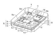
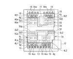
- FIG. 2 is an enlarged cross-sectional view taken along line AA in FIG. It is an expansion perspective view which shows the power semiconductor module of FIG. It is a top view except the insulating resin sealing member of the semiconductor device of FIG.
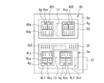
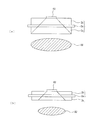
- FIG. 5 is a plan view showing an insulating substrate on which the semiconductor chip of FIG. 4 is mounted. It is explanatory drawing which shows the relationship between the thickness of the copper plate part which comprises an insulated substrate, and a heat-transfer area. It is an expanded sectional view which shows the conductor board for wiring. It is sectional drawing of a cooling body.
- FIG. 1 is a perspective view showing the overall configuration of a first embodiment of a semiconductor device according to the present invention
- FIG. 2 is a cross-sectional view taken along the line AA in FIG.
- reference numeral 1 denotes a semiconductor device.
- three power semiconductor modules 1 ⁇ / b> U, 1 ⁇ / b> V, and 1 ⁇ / b> W are fixed on a cooling body 21 at a predetermined interval in the longitudinal direction.
- Each of the power semiconductor modules 1U, 1V, and 1W has the same configuration. As shown in FIG.
- the semiconductor chip 4U and the lower arm constituting the upper arm are formed on the upper arm insulating substrate 3U and the lower arm insulating substrate 3L.
- a semiconductor chip 4L to be configured is mounted.
- the conductive posts 5Up and 5Lp as the conductive rod-like bodies are fixed on the respective semiconductor chips 4U1, 4U2, 4L1, and 4L2 at a predetermined interval.
- An upper arm wiring conductor plate 5U and a lower arm wiring conductor plate 5L as a second wiring conductor plate portion are disposed.
- each of the insulating substrates 3U and 3L is composed of an insulating plate portion 3a made of, for example, a silicon nitride substrate and, for example, a thick copper plate attached to the upper surface of the insulating plate portion 3a.
- the wiring pattern copper plate portion 3b and the heat radiating copper plate portion 3c which is similarly formed of a thick copper plate, are attached to the lower surface side of the insulating plate portion 3a.
- the wiring pattern copper plate portion 3b of the upper arm insulating substrate 3U is composed of the upper arm wiring pattern portion 3d as shown in FIG. 5, and the wiring pattern copper plate portion 3b of the lower arm insulating substrate 3L is The lower arm wiring pattern portion 3e and the grounding wiring pattern portion 3f are configured.
- the upper arm wiring pattern portion 3d is formed in a horizontally long rectangular shape when viewed from above, and is disposed on the upper surface of the wiring pattern copper plate portion 3b of the upper arm insulating substrate 3U.
- the lower arm wiring pattern portion 3e is formed in an L-shape when viewed from above with a rectangular chip mounting portion 3e1 and a connection portion 3e2 connected to the rear end surface on the left end side of the chip mounting portion 3e1.
- the wiring pattern copper plate portion 3b of the lower arm insulating substrate 3L is disposed on the upper surface.
- the ground wiring pattern portion 3f is formed in a horizontally long rectangle when viewed from above, and the rear end face of the chip mounting portion 3e1 of the lower arm wiring pattern portion 3e and the connection in the wiring pattern copper plate portion 3b of the lower arm insulating substrate 3L.
- the right end surface of the portion 3e2 is insulated from each other with a predetermined interval.
- the heat radiating copper plate portion 3c is arranged on the lower surface side of the insulating plate portions 3a of the respective insulating substrates 3U and 3L so as to overlap with the wiring pattern portions 3d, 3e, and 3f, respectively, as viewed from above.
- the wiring pattern copper plate portion 3b and the heat radiating copper plate portion 3c are formed of a copper plate having an equal thickness of, for example, 0.7 mm or more, preferably 1 mm or more in order to relieve thermal stress and suppress thermal resistance. Yes.
- the semiconductor chips 4U1, 4U2, 4L1, and 4L2 are mounted on the wiring pattern copper plate portion 3b as described later.
- heat generated in these semiconductor chips 4U1, 4U2, 4L1, and 4L2 diffuses through the wiring pattern copper plate portion 3b, the insulating plate portion 3a, and the heat dissipation copper plate portion 3c, as shown in FIG.
- the heat transfer area A1 when reaching the bottom surface of the heat radiating copper plate portion 3c can be widened.
- the wiring pattern copper plate portion 3b is set to 0.6 mm or less
- the heat transfer area A2 when reaching the bottom surface of the heat radiating copper plate portion 3c is as shown in FIG. It becomes narrower than the area A1.
- the individual thermal resistances Rth [K / W] of the insulating plate portion 3a, the wiring pattern copper plate portion 3b, and the heat dissipation copper plate portion 3c are set to t [m], and the thermal conductivity is ⁇ .
- [W / mK] is set and the heat transfer area on the bottom side is A [m 2 ]
- Rth t / ⁇ A (1)
- the overall thermal resistance of the insulating substrate 3 is the sum of the thermal resistances Rth of the plate portions 3a to 3c.
- the thermal conductivity ⁇ of the insulating plate portion 3a is smaller than the thermal conductivity of the copper plate, it is preferable to set the thickness t thin.
- the linear expansion coefficient ⁇ 1 of copper is 16 ppm to 18 ppm
- the linear expansion coefficient ⁇ 2 of the insulating plate portion 3a is 3 ppm to 5 ppm
- the aluminum serving as the cooling body 21 is about 22 ppm
- the space between the insulating plate portion 3a and the cooling body 21 is Thermal stress can be relieved by interposing the heat-dissipating copper plate portion 3c in the heat sink.
- the upper arm wiring pattern portion 3d incorporates two sets of reverse-conducting insulated gate bipolar transistors (hereinafter referred to as reverse-conducting IGBTs) constituting the upper arm.
- the semiconductor chips 4U1 and 4U2 thus mounted are mounted via a joining member such as solder.
- the chip mounting portion 3e1 of the lower arm wiring pattern portion 3e includes semiconductor chips 4L1 and 4L2 each including a pair of reverse conducting IGBTs constituting the lower arm, such as a bonding member such as solder.
- the reverse conducting IGBT is configured by integrating an IGBT and a free wheeling diode (FWD) reversely connected thereto into a single chip. For this reason, reverse conducting IGBT can reduce the area seen from the plane to about a half compared with the case where two semiconductor chips each incorporating IGBT and FWD are used.
- the positive-side connection terminal 11 constituting the main terminal is fixed to the upper arm wiring pattern portion 3d through a joining member such as solder.
- the output terminal 12 constituting the main terminal is fixed to the lower arm wiring pattern portion 3e through a joining member such as solder as shown by a two-dot chain line in FIG.
- the negative electrode side connection terminal 13 constituting the main terminal is fixed to the ground wiring pattern portion 3 f via a joining member such as solder.
- the upper arm wiring conductor plate 5U and the lower arm wiring conductor plate 5L are both formed of flat copper plates. As shown in FIG. 4, the upper arm wiring conductor plate 5U faces the semiconductor chip 4U1 and 4U2 from above, the chip facing plate portions 5U1 and 5U2, and the connection portion 3e2 of the lower arm wiring pattern portion 3e from above. And the connecting plate portion 5U3 to be connected to each other. Then, as shown in FIG. 4, chip opposing plate portions 5U1 and 5U2 are formed in a cylindrical shape as a conductive rod-like body on the emitter electrode 4Ue and the anode electrode 4Ua of the reverse conducting IGBT formed on the upper surfaces of the semiconductor chips 4U1 and 4U2. The plurality of conductive posts 5Up are electrically connected. Further, the connection plate portion 5U3 is electrically connected to the connection portion 3e2 of the lower arm wiring pattern portion 3e via a plurality of conductive posts 5Up as conductive rod-like bodies.
- each conductive post 5Up includes a large-diameter portion fitted in a through hole 15 formed on the inner arm surface of the upper arm wiring conductor plate 5U, for example, tin (Sn) plating. And a rod portion 17 serving as a small-diameter portion extending vertically from the center position of the upper and lower surfaces of the fitting portion 16.
- Each conductive post 5Up is fixed to the upper arm wiring conductor plate 5U by fitting the fitting portion 16 into the through hole 15, and the lower surface of the rod portion 17 protruding downward is the semiconductor chips 4U1, 4U2 and the lower arm.
- the wiring pattern part 3e is electrically connected to the connection part 3e2 by soldering, sintering metal fine particles, or the like.
- the conductive posts 5Up and 5U of the upper arm wiring conductor plate 5L and the lower arm wiring conductor plate 5L are applied on the solder paste in a state where the solder paste is applied to the joining positions of the conductive posts 5Up and 5Lp.
- the conductive posts 5Up and 5Lp can be soldered at a time. Note that the bar portion 17 extending above the conductive post 5Up can be omitted.
- the lower arm wiring conductor plate 5L includes a chip facing plate portion 5L1 facing the semiconductor chips 4L1 and 4L2, and a connecting plate portion 5L2 facing the right end side of the ground wiring pattern portion 3f. Are connected to each other.
- the chip opposing plate portion 5L1 is connected to the emitter electrode 4Le and the anode electrode 4La of the reverse conducting IGBT formed on the upper surfaces of the semiconductor chips 4L1 and 4L2 via the plurality of conductive posts 5Lp having the same configuration as the conductive post 5Up described above. They are electrically connected individually.
- the connection plate portion 5L2 is electrically connected to the right end side of the ground wiring pattern portion 3f via a plurality of conductive posts 5Lp having the same configuration as the conductive posts 5Up described above.
- the control electrodes such as the gate electrodes 4g and the emitter current sense electrodes 4es of the upper arm semiconductor chips 4U1 and 4U2 and the lower arm semiconductor chips 4L1 and 4L2 are connected to the external connection control terminal 19 via the lead frame 18. Yes.
- the insulating substrates 3U and 3L, the semiconductor chips 4U1 and 4U2, and the wiring conductor plates 5U and 5L are molded by the insulating resin sealing member 6, and the positive electrode side connection terminal 11, the output terminal 12 and the negative electrode side connection terminal 13 are externally connected.
- the connection control terminal 19 protrudes from the upper surface.
- the above is the specific configuration of the power semiconductor modules 1U, 1V, and 1W.
- These power semiconductor modules 1U, 1V, and 1W are joined to a cooling body 21 having a water-cooling jacket configuration with a metal sintered material.
- the bottom surface of the heat radiating copper plate portion 3c of the insulating substrate 3 of each power semiconductor module 1U, 1V, and 1W is in contact with a metal fine particle-containing paste containing metal fine particles such as Ag applied to the upper surface of the cooling body 21.
- a sintered metal material 20 formed by performing a sintering process under pressure and heating.
- the power semiconductor module 1U, 1V, and 1W heat radiating copper plate portion 3c is placed on the metal fine particle-containing paste and subjected to a sintering process to press and heat, thereby volatilizing the organic solvent and removing the metal fine particles.
- the sintered metal sintered material 20 it is possible to perform strong and high thermal conductivity bonding with a relatively thin bonding member layer of about 25 ⁇ m.
- a thin and uniform joining member layer can be formed with good reproducibility.
- the cooling body 21 includes a case body 22 formed by, for example, die-casting a metal material having a high thermal conductivity such as aluminum or aluminum alloy having a high thermal conductivity.
- An inlet 23 for injecting, for example, cooling water as a cooling medium is formed in one of the left and right ends of the case body 22, and an outlet 24 for discharging the cooling water is formed in the other.
- a cooling water passage 25 having an open upper end extending in the longitudinal direction is formed in an intermediate portion of the case body 22.
- the lid body 26 is fitted via a sealing member so as to close the cooling water passage 25.
- Cooling fins 27 projecting downward on the lower surface side and extending in the longitudinal direction are arranged on the lid body 26 at a predetermined interval in the width direction. Cooling water flows between the cooling fins 27. And the power semiconductor modules 1U, 1V, and 1W are joined to the upper surface of the cover body 26 by the metal sintered material 20 by the sintering process using metal microparticles.
- the connecting portion between the inlet 23 of the case body 22 and the cooling water passage 25 is configured as shown in FIG.
- the inlet 23 having a large inner diameter and the cooling water passage 25 having a thickness smaller than that of the inlet 23 are arranged in a stepped manner such that a part thereof overlaps in the vertical direction.
- a step portion 28 is formed between the bottom portion of the inlet 23 and the bottom portion of the cooling water passage 25 where the cooling water injected from the cooling water passage 25 becomes a champ in the width direction. For this reason, the cooling water injected from the injection port 23 abuts on the step portion 28 and spreads in the width direction of the cooling body 21, and the cooling water is uniformly passed in the width direction to the cooling water passage 25. Can be cooled uniformly.
- the equivalent circuit of each of the power semiconductor modules 1U to 1W includes an upper arm between a positive side connection terminal 11 constituting the main terminal and a negative side connection terminal 13 constituting the main terminal.
- the reverse conducting IGBT QU that constitutes the lower conducting arm and the reverse conducting IGBT QL that constitutes the lower arm are connected in series. Therefore, for example, in a state where a low level gate voltage is supplied to the gate electrode 4g of the reverse conduction IGBTQL of the lower arm and the gate electrode 4g of the reverse conduction IGBTQU of the upper arm is turned off, In addition, the switching state is set.
- the current from the positive electrode side connection terminal 11 is supplied to each of the upper arm semiconductor chips 4U1 and 4U2 through the upper arm wiring pattern portion 3d of the upper arm insulating substrate 3U. Input to the collector electrode of the built-in reverse conducting IGBT. Then, it is output from the emitter electrode through the collector electrode of the reverse conducting IGBT as shown in FIGS. As shown in FIG. 11 (b), the current output from the emitter electrode passes through the chip opposing plate portions 5U1 and 5U2 of the upper arm wiring conductor plate 5U, and further through the connection plate portion 5U3 to the lower arm insulating substrate 3L. Supplied to the connecting portion 3e2 of the lower arm wiring pattern portion 3e.
- the current supplied to the connection portion 3e2 passes through the lower arm wiring pattern portion 3e and is output as shown in FIGS. 13A and 13B. Output from the terminal 12.
- the gate electrode 4g of the reverse conducting IGBT QUA constituting the upper arm and the reverse conducting IGBT QUA is turned off the gate electrode 4g of the reverse conducting IGBT QL constituting the lower arm is applied.
- a gate voltage that repeatedly turns on and off is applied to establish a switching state.
- the reverse conducting IGBT QL is turned on, as shown in FIGS. 14A and 14B, the current input from the output terminal 12 is the lower arm wiring pattern of the lower arm insulating substrate 3L.
- the signal is input to the collector electrode of the reverse conducting IGBT QL constituting the lower arm through the part 3e.
- the current input to the collector of the reverse conducting IGBT QL is output from the upper emitter electrode 4Le, and as shown in FIGS. 15A and 15B, through the lower arm wiring conductor plate 5L, FIGS.
- the negative electrode side connection terminal 13 flows through the ground wiring pattern portion 3f formed on the lower arm insulating substrate 3L as shown in FIGS. 17A and 17B. 13 returns to the negative side of the power source.
- a one-phase portion of a three-phase alternating current is formed by the reverse conducting IGBT constituting the upper arm and the lower arm.
- the three power semiconductor modules 1U to 1W are controlled to be turned on / off by gate signals shifted by 120 degrees, so that a three-phase alternating current of U phase, V phase, and W phase can be output to the load.
- the semiconductor chips 4U1, 4U2 and 4L1, 4L2 incorporating the reverse conducting IGBTs QU and QL are in a heat generating state.
- the heat generated by each of these semiconductor chips 4U1, 4U2, 4L1, and 4L2 passes through the upper arm wiring pattern portion 3d and the lower arm wiring pattern portion 3e, through the insulating plate portion 3a, and further to the heat dissipation copper plate portion.
- heat conduction is performed to the lid body 26 of the cooling body 21 through the metal sintered material 20 obtained by sintering the metal fine particles. Then, the heat transferred to the lid body 26 is cooled by the cooling fins 27 that are in contact with the cooling water.
- the upper arm insulating substrate 3U and the lower arm insulating substrate 3L on which the semiconductor chips 4U1, 4U2 and 4L1, 4L2 that generate heat are mounted are placed on the front and back of the insulating plate portion 3a and the insulating plate portion 3a, which are relatively thin.
- the wiring pattern copper plate portion 3b and the heat radiating copper plate portion 3c are formed. Since the thickness of the wiring pattern copper plate portion 3b and the heat radiation copper plate portion 3c constituting the upper arm wiring pattern portion 3d and the lower arm wiring pattern portion 3e is 0.7 mm or more, preferably 1 mm or more. As described above, the thermal stress can be relaxed and the thermal resistance can be suppressed to improve the heat conduction efficiency.
- the organic solvent is evaporated by heating to 250 ° C. Since the pressure and heat bonding is performed to sinter, the bonding strength can be ensured while the thickness at the bonding portion is reduced, and the thermal conductivity can be increased.
- the heat generated in each of the semiconductor chips 4U1, 4U2 and 4L1, 4L2 can be transferred to the cooling body 21 with high heat conduction efficiency, and good cooling can be performed by the cooling body 21, and each of the semiconductor chips 4U1, 4U2, and It is possible to reliably prevent 4L1 and 4L2 from being overheated. Further, by applying reverse conducting IGBTQU and QL as switching elements built in the semiconductor chips 4U1, 4U2 and 4L1, 4L2, the chip area is about 50% as compared with the case where the IGBT and FWD are built in individual semiconductor chips. The power semiconductor modules 1U to 1W can be reduced in size accordingly.
- a thin bonding wire is used for the current paths between the semiconductor chips 4U1, 4U2 and 4L1, 4L2 and the positive connection terminal 11, the output terminal 12 and the negative connection terminal 13 as external connection terminals.
- the upper arm wiring conductor plate 5U and the lower arm wiring conductor plate 5L each including the rod-like conductive posts 5Up and 5Lp, and the upper arm wiring pattern portion 3d and the lower arm wiring pattern portion made of a copper plate, respectively. 3e and the grounding wiring pattern portion 3f, the wiring inductance can be reduced from 20 to 40 nH when bonding wires are used to about 1 to 2 nH. For this reason, switching speed can be improved.
- the lead frame 18 is used for connecting the control terminals of the semiconductor chips 4U1, 4U2 and 4L1, 4L2 and the external connection control terminal 19 without using the bonding wire, the generated Joule heat is used for the bonding wire. It can be made smaller compared to
- the configuration of the cooling body 21 is changed to an integrated type. That is, in the second embodiment, as shown in FIGS. 18 and 19, the cooling body 21 is directly divided into the cooling water passage 25 of the case body 22 without dividing the cooling body 21 into the case body 22 and the lid body 26. A large number of partition walls 31 are formed at predetermined intervals in the width direction. Then, the power semiconductor modules 1U to 1W having the same configuration as that of the first embodiment described above are joined to the upper surface of the case body 22 with a joining member that is sintered by pressing and heating metal fine particles such as Ag. .
- the power semiconductor modules 1U to 1W are joined to the cooling body 21 with a joining member obtained by sintering metal fine particles, so that the thermal conductivity of the joining member can be increased. In addition, a strong bond can be obtained.
- the cooling body 21 has an integrated structure in which no opening is present, it is possible to reliably avoid a cooling medium such as cooling water from leaking to the outside.
- the present invention is not limited to this, and various types of power semiconductor modules such as the 1in1 type, the 4in1 type, and the 6in1 type are used. The present invention can be applied to.
- the number of semiconductor chips constituting each arm is not limited to two, and the number of semiconductor chips arranged in parallel can be arbitrarily set according to the amount of current used. Accordingly, the number of conductive posts can be set to an arbitrary number according to the current used. Furthermore, in the above embodiment, the case where the three power semiconductor modules 1U to 1W are mounted on the cooling body 21 has been described. However, the present invention is not limited to this, and an arbitrary number of power semiconductor modules can be used depending on the application. Can be placed.
- the present invention is not limited to this, and the upper arm insulating substrate 3U, the lower arm insulating substrate 3L, and the semiconductor chips 4U1, 4U2 are not limited thereto.
- 4L1, 4L2, the upper arm wiring conductor plate 5U, and the lower arm wiring conductor plate 5L may be covered with a case, and the inside of the case may be filled with a gel-like sealing member.
- a wiring pattern copper plate portion including a plurality of wiring patterns of an upper arm wiring pattern portion 3d, a lower arm wiring pattern portion 3e, and a grounding wiring pattern portion 3f is formed on a single insulating plate portion, You may make it form the common heat-transfer pattern (heat-dissipation copper plate part) 3c for heat dissipation.
- ceramic base materials such as alumina (Al 2 O 3 ) and aluminum nitride (AlN) can be applied as the insulating plate portions 3a of the insulating substrates 3U and 3L.
- cylindrical conductive post 5Up and 5Lp are applied as the insulating plate portions 3a of the insulating substrates 3U and 3L.
- Conductive posts can be applied.
- the conductive posts 5Up and 5Lp may be conductive rod-shaped bodies that contribute to a reduction in inductance.
- a printed circuit board can be applied in place of the upper arm wiring conductor plate 5U and the lower arm wiring conductor plate 5L made of a copper plate.
- the present invention can obtain a desired circuit configuration only by the combination of terminal connections of the power semiconductor module. Therefore, the present invention is not limited to the above-described inverter device for power conversion but uses a power semiconductor module. The present invention can be applied to other semiconductor devices such as other power conversion devices and switching ICs for high frequency applications.
- connection terminal 17 ... external Auxiliary connection terminal, 20 ... sintered metal, 21 ... cooling body, 22 ... case body, 23 ... inlet, 24 ... discharge port, 25 ... cooling water passage, 26 ... lid, 27 ... cooling fin
Landscapes
- Cooling Or The Like Of Semiconductors Or Solid State Devices (AREA)
- Inverter Devices (AREA)
- Chemical & Material Sciences (AREA)
- Engineering & Computer Science (AREA)
- Ceramic Engineering (AREA)
- Physics & Mathematics (AREA)
- Geometry (AREA)
Abstract
保持手段を設けることがなく絶縁基板と冷却体とを熱抵抗を小さくして確実に接合することができる半導体装置を提供する。絶縁板部の一方に複数の配線パターンを形成する配線パターン用銅板部を配置し、他方に放熱用銅板部を配置した絶縁基板(3U),(3L)と、該絶縁基板の前記配線パターン用銅板部に実装された半導体チップ(4U),(4L)と、前記絶縁基板の放熱用銅板部に接触された冷却体(21)と、前記半導体チップと前記配線パターン用銅板部との間に接続された配線用導体板(5U),(5L)とを備え、前記絶縁基板の放熱用銅板部と前記冷却体とを金属焼結材(20)で接合するとともに、前記配線パターン用銅板部及び前記放熱用銅板部の厚みが熱応力を緩和する厚みに設定されている。
Description
本発明は、パワーデバイス、高周波用途のスイッチングICなどの半導体装置に関し、特にパワー半導体素子を搭載した半導体装置に関する。
インバータ装置、無停電電源装置、工作機械、産業用ロボット等では、その本体装置とは独立して半導体装置(パワー半導体モジュール)が使用されている。
従来の半導体装置としては、例えば特許文献1に記載されているパワーモジュールが知られている。
このパワーモジュールは、セラミックス基板の両面に金属層が接合されたパワーモジュール基板と、一方の金属層にAgの仮焼結層を介在させることにより仮止め状態に接合されたヒートシンクと、パワーモジュール基板とヒートシンクとを積層状態に保持する保持手段とを備えている。
従来の半導体装置としては、例えば特許文献1に記載されているパワーモジュールが知られている。
このパワーモジュールは、セラミックス基板の両面に金属層が接合されたパワーモジュール基板と、一方の金属層にAgの仮焼結層を介在させることにより仮止め状態に接合されたヒートシンクと、パワーモジュール基板とヒートシンクとを積層状態に保持する保持手段とを備えている。
ところで、上記特許文献1に記載されている従来例では、セラミックス基板の割れや接合部の剥離を防止するために、パワーモジュール基板の金属層とヒートシンクとをAgの仮焼結層で連結し、パワーモジュール基板とヒートシンクとの積層状態は別途保持手段によって保持するようにしている。
しかしながら、上記従来例にあっては、パワーモジュール基板の金属層とヒートシンクとを外力によって原料粉末が僅かに流動するようにAgの仮焼結層で結合しているので、完全な焼結層とする場合に比較して熱抵抗が大きくなるとともに、別途パワーモジュール基板とヒートシンクとを強固に保持する保持手段を必要とし、全体の構成が大型化するという未解決の課題がある。
そこで、本発明は、上記従来例の未解決の課題に着目してなされたものであり、保持手段を設けることがなく絶縁基板と冷却体とを熱抵抗を小さくして確実に接合することができる半導体装置を提供することを目的としている。
しかしながら、上記従来例にあっては、パワーモジュール基板の金属層とヒートシンクとを外力によって原料粉末が僅かに流動するようにAgの仮焼結層で結合しているので、完全な焼結層とする場合に比較して熱抵抗が大きくなるとともに、別途パワーモジュール基板とヒートシンクとを強固に保持する保持手段を必要とし、全体の構成が大型化するという未解決の課題がある。
そこで、本発明は、上記従来例の未解決の課題に着目してなされたものであり、保持手段を設けることがなく絶縁基板と冷却体とを熱抵抗を小さくして確実に接合することができる半導体装置を提供することを目的としている。
上記目的を達成するために、本発明に係る半導体装置の第1の態様は、絶縁板部の一方に配線パターンを形成する配線パターン用銅板部を配置し、他方に放熱用銅板部を配置した絶縁基板と、この絶縁基板の配線パターン用銅板部に実装された半導体チップと、絶縁基板の放熱用銅板部に接合された冷却体と、半導体チップと配線パターン用銅板部とに接続された配線用導体板とを備えている。そして、絶縁基板の放熱用銅板部と冷却体とを金属焼結材で接合するとともに、配線パターン用銅板部及び放熱用銅板部の厚みが熱応力を緩和する厚みに設定されている。
また、本発明に係る半導体装置の第2の態様は、前記配線パターン用銅板部及び前記放熱用銅板部の厚みが熱応力を緩和し、且つ熱抵抗を抑制する厚みに設定されている。
また、本発明に係る半導体装置の第3の態様は、前記配線用導体板と前記半導体チップ及び前記配線パターン用銅板部との電気的接続が導電性棒状体を介して行われている。
また、本発明に係る半導体装置の第4の態様は、前記導電性棒状体が、前記半導体チップ及び配線パターン用銅板部と前記配線用銅体板との間の棒部の断面積に比較して前記配線用導体板に嵌合する嵌合部の断面積が広く設定された構成を有している。
また、本発明に係る半導体装置の第5の態様は、前記半導体チップが、絶縁ゲートバイポーラトランジスタとこれに逆接続したフリー・ホイーリング・ダイオードとをワンチップ化して構成されている。
また、本発明に係る半導体装置の第3の態様は、前記配線用導体板と前記半導体チップ及び前記配線パターン用銅板部との電気的接続が導電性棒状体を介して行われている。
また、本発明に係る半導体装置の第4の態様は、前記導電性棒状体が、前記半導体チップ及び配線パターン用銅板部と前記配線用銅体板との間の棒部の断面積に比較して前記配線用導体板に嵌合する嵌合部の断面積が広く設定された構成を有している。
また、本発明に係る半導体装置の第5の態様は、前記半導体チップが、絶縁ゲートバイポーラトランジスタとこれに逆接続したフリー・ホイーリング・ダイオードとをワンチップ化して構成されている。
また、本発明に係る半導体装置の第6の態様は、前記配線パターン用銅板部及び前記放熱用銅板部の厚みが0.7mm以上に設定されている。
また、本発明に係る半導体装置の第7の態様は、前記絶縁基板の配線パターン用銅板部が、上アームを構成する半導体チップを実装する上アーム用配線パターン部と、下アームを構成する半導体チップを実装する下アーム用配線パターン部と、接地用配線パターン部とが互いに独立して前記絶縁板部上に形成されている。
また、本発明に係る半導体装置の第8の態様は、前記上アーム用配線パターン部に正極側接続端子が接続され、前記下アーム用配線パターンに出力端子が接続され、前記接地用配線パターン部に負極側接続端子が接続されている。
また、本発明に係る半導体装置の第9の態様は、前記配線用導体板は、前記上アームを構成する半導体チップと前記下アーム用配線パターン部とを接続する第1の配線用導体板部と、前記下アームを構成する半導体チップと前記接地用配線パターン部とを接続する第2の配線用導体板部とで構成されている。
また、本発明に係る半導体装置の第7の態様は、前記絶縁基板の配線パターン用銅板部が、上アームを構成する半導体チップを実装する上アーム用配線パターン部と、下アームを構成する半導体チップを実装する下アーム用配線パターン部と、接地用配線パターン部とが互いに独立して前記絶縁板部上に形成されている。
また、本発明に係る半導体装置の第8の態様は、前記上アーム用配線パターン部に正極側接続端子が接続され、前記下アーム用配線パターンに出力端子が接続され、前記接地用配線パターン部に負極側接続端子が接続されている。
また、本発明に係る半導体装置の第9の態様は、前記配線用導体板は、前記上アームを構成する半導体チップと前記下アーム用配線パターン部とを接続する第1の配線用導体板部と、前記下アームを構成する半導体チップと前記接地用配線パターン部とを接続する第2の配線用導体板部とで構成されている。
本発明によれば、絶縁基板の放熱用銅板部と冷却体とを焼結接続した状態でも放熱用銅板部及び配線パターン用銅板部で熱応力を緩和することができる。このため、絶縁基板と冷却体とを保持する保持手段を設ける必要なく、絶縁基板の絶縁板部の割れや接合部の剥離を防止することができ、放熱効果を確保しながら全体の構成を小型化することができる。
以下、図面を参照してこの発明の実施の形態について説明する。
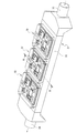
図1は本発明に係る半導体装置の第1の実施形態における全体構成を示す斜視図、図2は図1のA-A線上の断面図である。
図1において、1は半導体装置であって、この半導体装置1は、3つのパワー半導体モジュール1U、1V及び1Wが冷却体21上に長手方向に所定間隔を保って固定されている。
各パワー半導体モジュール1U、1V及び1Wは同一構成を有し、図2に示すように、上アーム用絶縁基板3U及び下アーム用絶縁基板3L上に上アームを構成する半導体チップ4U及び下アームを構成する半導体チップ4Lが実装されている。図3~図5に示すように、各半導体チップ4U1,4U2,4L1,4L2上に所定間隔を保って導電性棒状体としての導電ポスト5Up及び5Lpを固定した第1の配線用導体板部としての上アーム配線用導体板5U及び第2の配線用導体板部としての下アーム配線用導体板5Lが配置されている。
図1は本発明に係る半導体装置の第1の実施形態における全体構成を示す斜視図、図2は図1のA-A線上の断面図である。
図1において、1は半導体装置であって、この半導体装置1は、3つのパワー半導体モジュール1U、1V及び1Wが冷却体21上に長手方向に所定間隔を保って固定されている。
各パワー半導体モジュール1U、1V及び1Wは同一構成を有し、図2に示すように、上アーム用絶縁基板3U及び下アーム用絶縁基板3L上に上アームを構成する半導体チップ4U及び下アームを構成する半導体チップ4Lが実装されている。図3~図5に示すように、各半導体チップ4U1,4U2,4L1,4L2上に所定間隔を保って導電性棒状体としての導電ポスト5Up及び5Lpを固定した第1の配線用導体板部としての上アーム配線用導体板5U及び第2の配線用導体板部としての下アーム配線用導体板5Lが配置されている。
そして、絶縁基板3U,3L、半導体チップ4U1,4U2,4L1,4L2、上アーム配線用導体板5U及び下アーム配線用導体板5Lが例えば熱硬化性樹脂のエポキシ樹脂材料でなる絶縁樹脂封止部材6によって絶縁基板3U及び3Lの底面を露出した状態で封止されている。
絶縁基板3U及び3Lのそれぞれは、図2及び図3に示すように、例えば窒化珪素基板で構成される絶縁板部3aと、この絶縁板部3aの上面に貼り付けられた例えば厚銅板で構成される配線パターン用銅板部3bと、絶縁板部3aの下面側に貼り付けられた同様に厚銅板で構成される放熱用銅板部3cとで構成されている。
絶縁基板3U及び3Lのそれぞれは、図2及び図3に示すように、例えば窒化珪素基板で構成される絶縁板部3aと、この絶縁板部3aの上面に貼り付けられた例えば厚銅板で構成される配線パターン用銅板部3bと、絶縁板部3aの下面側に貼り付けられた同様に厚銅板で構成される放熱用銅板部3cとで構成されている。
ここで、上アーム用絶縁基板3Uの配線パターン用銅板部3bは、図5に示すように、上アーム用配線パターン部3dで構成され、下アーム用絶縁基板3Lの配線パターン用銅板部3bは、下アーム用配線パターン部3eと、接地用配線パターン部3fとで構成されている。
上アーム用配線パターン部3dは、平面から見て横長の長方形状に形成され、上アーム用絶縁基板3Uの配線パターン用銅板部3bの上面に配置されている。
下アーム用配線パターン部3eは、長方形状のチップ搭載部3e1とこのチップ搭載部3e1の左端側における後方側端面に連接された接続部3e2とで平面から見てL字状に形成されて、下アーム用絶縁基板3Lの配線パターン用銅板部3bの上面に配置されている。
接地用配線パターン部3fは、平面から見て横長の長方形に形成され、下アーム用絶縁基板3Lの配線パターン用銅板部3bにおける下アーム用配線パターン部3eのチップ搭載部3e1の後端面及び接続部3e2の右端面にそれぞれ所定間隔を保って絶縁されて配置されている。
上アーム用配線パターン部3dは、平面から見て横長の長方形状に形成され、上アーム用絶縁基板3Uの配線パターン用銅板部3bの上面に配置されている。
下アーム用配線パターン部3eは、長方形状のチップ搭載部3e1とこのチップ搭載部3e1の左端側における後方側端面に連接された接続部3e2とで平面から見てL字状に形成されて、下アーム用絶縁基板3Lの配線パターン用銅板部3bの上面に配置されている。
接地用配線パターン部3fは、平面から見て横長の長方形に形成され、下アーム用絶縁基板3Lの配線パターン用銅板部3bにおける下アーム用配線パターン部3eのチップ搭載部3e1の後端面及び接続部3e2の右端面にそれぞれ所定間隔を保って絶縁されて配置されている。
また、放熱用銅板部3cは、各絶縁基板3U及び3Lの絶縁板部3aの下面側で、夫々配線パターン部3d及び3e,3fと平面から見て重なるように配置されている。
ここで、配線パターン用銅板部3b及び放熱用銅板部3cは、熱応力を緩和し、且つ熱抵抗を抑制するために、例えば0.7mm以上好ましくは1mm以上の等しい厚みの銅板で形成されている。このように、配線パターン用銅板部3b及び放熱用銅板部3cの厚みを0.7mm以上設定すると、後述するように、配線パターン用銅板部3bに半導体チップ4U1,4U2,4L1,4L2を実装したときに、これら半導体チップ4U1,4U2,4L1,4L2で発生する熱が、図6(a)に示すように、配線パターン用銅板部3b、絶縁板部3a及び放熱用銅板部3cを介して拡散して行き、放熱用銅板部3cの底面に達したときの伝熱面積A1を広くとすることができる。これに対して、配線パターン用銅板部3bを0.6mm以下に設定すると、図6(b)に示すように、放熱用銅板部3cの底面に達したときの伝熱面積A2が上記伝熱面積A1より狭くなる。
ここで、配線パターン用銅板部3b及び放熱用銅板部3cは、熱応力を緩和し、且つ熱抵抗を抑制するために、例えば0.7mm以上好ましくは1mm以上の等しい厚みの銅板で形成されている。このように、配線パターン用銅板部3b及び放熱用銅板部3cの厚みを0.7mm以上設定すると、後述するように、配線パターン用銅板部3bに半導体チップ4U1,4U2,4L1,4L2を実装したときに、これら半導体チップ4U1,4U2,4L1,4L2で発生する熱が、図6(a)に示すように、配線パターン用銅板部3b、絶縁板部3a及び放熱用銅板部3cを介して拡散して行き、放熱用銅板部3cの底面に達したときの伝熱面積A1を広くとすることができる。これに対して、配線パターン用銅板部3bを0.6mm以下に設定すると、図6(b)に示すように、放熱用銅板部3cの底面に達したときの伝熱面積A2が上記伝熱面積A1より狭くなる。
ここで、絶縁板部3a、配線パターン用銅板部3b及び放熱用銅板部3cの個々の熱抵抗Rth[K/W]は、伝熱体の厚みをt[m]とし、熱伝導率をλ[W/mK]とし、底面側の伝熱面積をA[m2]としたとき、下記(1)式で表される。
Rth=t/λA …………(1)
このため、厚みの変化に対して伝熱面積の変化の方が大きいので、厚みが厚くなるほど熱抵抗Rthが小さく抑制され、放熱効果を向上させることができる。
そして、絶縁基板3全体の熱抵抗は各板部3a~3cの熱抵抗Rthの和となる。ここに、絶縁板部3aについては熱伝導率λが銅板の熱伝導率に比較して小さいので、厚みtを薄く設定した方が好ましい。
Rth=t/λA …………(1)
このため、厚みの変化に対して伝熱面積の変化の方が大きいので、厚みが厚くなるほど熱抵抗Rthが小さく抑制され、放熱効果を向上させることができる。
そして、絶縁基板3全体の熱抵抗は各板部3a~3cの熱抵抗Rthの和となる。ここに、絶縁板部3aについては熱伝導率λが銅板の熱伝導率に比較して小さいので、厚みtを薄く設定した方が好ましい。
そして、温度上昇分ΔTは、デバイス損失をQ〔W〕とすると、下記(2)式のように熱抵抗Rthにデバイス損失Qを乗算した値となる。
ΔT=Rth×Q …………(2)
したがって、デバイス損失は定数であるので、熱抵抗Rthが小さい値となると温度上昇分ΔTを抑制して、良好な放熱効果を得ることができる。
また、銅の線膨張係数α1は16ppm~18ppm、絶縁板部3aの線膨張係数α2は3ppm~5ppm、冷却体21となるアルミニウムは22ppm程度であり、絶縁板部3aと冷却体21との間に放熱用銅板部3cを介在させることにより、熱応力を緩和することができる。
ΔT=Rth×Q …………(2)
したがって、デバイス損失は定数であるので、熱抵抗Rthが小さい値となると温度上昇分ΔTを抑制して、良好な放熱効果を得ることができる。
また、銅の線膨張係数α1は16ppm~18ppm、絶縁板部3aの線膨張係数α2は3ppm~5ppm、冷却体21となるアルミニウムは22ppm程度であり、絶縁板部3aと冷却体21との間に放熱用銅板部3cを介在させることにより、熱応力を緩和することができる。
したがって、配線パターン用銅板部3b及び放熱用銅板部3cの厚みを0.6mm以下とすると、十分な放熱効果が得られないとともに、銅板部が変形し易くなり、熱応力の緩和に寄与しなくなるが、厚みを0.7mm以上とすることにより、十分な放熱効果と熱応力の緩和を同時に行うことができる。
そして、上アーム用配線パターン部3dには、図5に示すように、上アームを構成する2組の逆導通絶縁ゲートバイポーラトランジスタ(Insulated Gate Bipolar Transistor)(以下、逆導通IGBTと称す)を内蔵した半導体チップ4U1及び4U2が例えば半田等の接合部材を介して実装されている。
そして、上アーム用配線パターン部3dには、図5に示すように、上アームを構成する2組の逆導通絶縁ゲートバイポーラトランジスタ(Insulated Gate Bipolar Transistor)(以下、逆導通IGBTと称す)を内蔵した半導体チップ4U1及び4U2が例えば半田等の接合部材を介して実装されている。
また、下アーム用配線パターン部3eのチップ搭載部3e1には、図5に示すように、下アームを構成する2組の逆導通IGBTを内蔵した半導体チップ4L1及び4L2が例えば半田等の接合部材を介して実装されている。
ここで、逆導通IGBTは、IGBTとこれに逆接続したフリー・ホイーリング・ダイオード(Free Wheeling Diode,FWD)とをワンチップ化して構成されている。このため、逆導通IGBTは、IGBTとFWDとを個別に内蔵させた2つの半導体チップを使用する場合に比較して平面から見た面積を半分程度に低減することができる。
さらに、上アーム用配線パターン部3dには、図5において二点鎖線で図示したように、主端子を構成する正極側接続端子11が半田等の接合部材を介して固定されている。同様に下アーム用配線パターン部3eには、図5において二点鎖線で図示したように主端子を構成する出力端子12が半田等の接合部材を介して固定されている。さらに、接地用配線パターン部3fには図5において二点鎖線で図示したように、主端子を構成する負極側接続端子13が半田等の接合部材を介して固定されている。
ここで、逆導通IGBTは、IGBTとこれに逆接続したフリー・ホイーリング・ダイオード(Free Wheeling Diode,FWD)とをワンチップ化して構成されている。このため、逆導通IGBTは、IGBTとFWDとを個別に内蔵させた2つの半導体チップを使用する場合に比較して平面から見た面積を半分程度に低減することができる。
さらに、上アーム用配線パターン部3dには、図5において二点鎖線で図示したように、主端子を構成する正極側接続端子11が半田等の接合部材を介して固定されている。同様に下アーム用配線パターン部3eには、図5において二点鎖線で図示したように主端子を構成する出力端子12が半田等の接合部材を介して固定されている。さらに、接地用配線パターン部3fには図5において二点鎖線で図示したように、主端子を構成する負極側接続端子13が半田等の接合部材を介して固定されている。
また、上アーム配線用導体板5U及び下アーム配線用導体板5Lは、ともに扁平な銅板で構成されている。上アーム配線用導体板5Uは、図4に示すように、半導体チップ4U1及び4U2に上方から対向するチップ対向板部5U1及び5U2と、下アーム用配線パターン部3eの接続部3e2に上方から対向する接続板部5U3とが互いに接続された構成を有する。
そして、図4に示すように、半導体チップ4U1及び4U2の上面に形成された逆導通IGBTのエミッタ電極4Ue及びアノード電極4Uaにチップ対向板部5U1及び5U2が導電性棒状体としての円柱状に形成された複数の導電ポスト5Upを介して電気的に接続されている。また、接続板部5U3が下アーム用配線パターン部3eの接続部3e2に導電性棒状体としての複数の導電ポスト5Upを介して電気的に接続されている。
そして、図4に示すように、半導体チップ4U1及び4U2の上面に形成された逆導通IGBTのエミッタ電極4Ue及びアノード電極4Uaにチップ対向板部5U1及び5U2が導電性棒状体としての円柱状に形成された複数の導電ポスト5Upを介して電気的に接続されている。また、接続板部5U3が下アーム用配線パターン部3eの接続部3e2に導電性棒状体としての複数の導電ポスト5Upを介して電気的に接続されている。
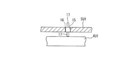
各導電ポスト5Upは、図7に示すように、上アーム配線用導体板5Uに形成された例えば内周面に錫(Sn)メッキが施された貫通孔15に嵌合される大径部となる嵌合部16と、この嵌合部16の上下面の中心位置から上下に延長する小径部となる棒部17とで構成されている。
そして、各導電ポスト5Upは上アーム配線用導体板5Uに、嵌合部16を貫通孔15に嵌合させて固定され、下方に突出する棒部17の下面が半導体チップ4U1,4U2及び下アーム用配線パターン部3eの接続部3e2に個別に半田付け,金属微粒子の焼結等によって電気的に接合されている。半田付けを行う場合に、各導電ポスト5Up及び5Lpの接合位置に半田ペーストを塗布した状態で、半田ペースト上に各上アーム配線用導体板5U及び下アーム配線用導体板5Lの導電ポスト5Up及び5Lpを載置してからリフロー処理することにより、各導電ポスト5Up及び5Lpを一度に半田付けすることができる。なお、導電ポスト5Upの上方に延長する棒部17は省略することができる。
そして、各導電ポスト5Upは上アーム配線用導体板5Uに、嵌合部16を貫通孔15に嵌合させて固定され、下方に突出する棒部17の下面が半導体チップ4U1,4U2及び下アーム用配線パターン部3eの接続部3e2に個別に半田付け,金属微粒子の焼結等によって電気的に接合されている。半田付けを行う場合に、各導電ポスト5Up及び5Lpの接合位置に半田ペーストを塗布した状態で、半田ペースト上に各上アーム配線用導体板5U及び下アーム配線用導体板5Lの導電ポスト5Up及び5Lpを載置してからリフロー処理することにより、各導電ポスト5Up及び5Lpを一度に半田付けすることができる。なお、導電ポスト5Upの上方に延長する棒部17は省略することができる。
また、下アーム配線用導体板5Lは、図4に示すように、半導体チップ4L1及び4L2に対向するチップ対向板部5L1と、接地用配線パターン部3fの右端側に対向する接続板部5L2とが互いに連結された構成を有する。
そして、チップ対向板部5L1が半導体チップ4L1及び4L2の上面に形成された逆導通IGBTのエミッタ電極4Le及びアノード電極4Laに前述した導電ポスト5Upと同様の構成を有する複数の導電ポスト5Lpを介して個別に電気的に接続されている。また、接続板部5L2が接地用配線パターン部3fの右端側に前述した導電ポスト5Upと同様の構成を有する複数の導電ポスト5Lpを介して電気的に接続されている。
そして、チップ対向板部5L1が半導体チップ4L1及び4L2の上面に形成された逆導通IGBTのエミッタ電極4Le及びアノード電極4Laに前述した導電ポスト5Upと同様の構成を有する複数の導電ポスト5Lpを介して個別に電気的に接続されている。また、接続板部5L2が接地用配線パターン部3fの右端側に前述した導電ポスト5Upと同様の構成を有する複数の導電ポスト5Lpを介して電気的に接続されている。
また、上アーム用半導体チップ4U1及び4U2と下アーム用半導体チップ4L1及び4L2のゲート電極4g及びエミッタ電流センス電極4es等の制御電極がリードフレーム18を介して外部接続用制御端子19に接続されている。
そして、絶縁基板3U,3L、半導体チップ4U1,4U2、配線用導体板5U,5Lが絶縁樹脂封止部材6によってモールド成型され、正極側接続端子11、出力端子12及び負極側接続端子13と外部接続用制御端子19が上面から突出されている。
そして、絶縁基板3U,3L、半導体チップ4U1,4U2、配線用導体板5U,5Lが絶縁樹脂封止部材6によってモールド成型され、正極側接続端子11、出力端子12及び負極側接続端子13と外部接続用制御端子19が上面から突出されている。
以上がパワー半導体モジュール1U、1V及び1Wの具体的構成である。これらパワー半導体モジュール1U、1V及び1Wは水冷ジャケットの構成を有する冷却体21に金属焼結材で接合されている。各パワー半導体モジュール1U、1V及び1Wの絶縁基板3の放熱用銅板部3cの底面は、冷却体21の上面に塗布された例えばAg等の金属微粒子を含有する金属微粒子含有ペーストに接触させた状態で、加圧加熱する焼結処理を行って形成した金属焼結材20により接合されている。このように、パワー半導体モジュール1U、1V及び1Wの放熱用銅板部3cを金属微粒子含有ペースト上に載置して加圧加熱する焼結処理を行うことにより、有機溶剤を揮発させて金属微粒子を焼結した金属焼結材20として、25μm程度の比較的薄い接合部材層で強固で且つ熱伝導率の高い接合を行うことができる。配線パターン用銅板部3b及び放熱用銅板部3cの厚みを0.7mm以上と厚くすることにより、薄く均一な接合部材層を再現性よく形成することができる。
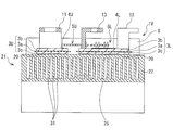
この冷却体21は、図1に示すように、例えば熱伝導率の高いアルミニウム、アルミニウム合金等の高熱伝導率の金属材料を例えばダイキャスト成型して形成されたケース体22を有する。このケース体22の左右両端部の一方に冷却媒体としての例えば冷却水を注入する注入口23が形成され、他方に冷却水を排出する排出口24が形成されている。
ケース体22の中間部には、図2に示すように、長手方向に延長する上端を開放した冷却水通路25が形成されている。そして、蓋体26が冷却水通路25を閉塞するように封止部材を介して嵌合されている。この蓋体26には、下面側に下方に突出し、且つ長手方向に延長する冷却フィン27が幅方向に所定間隔を保って配置されている。各冷却フィン27間には冷却水が通流するように構成されている。
そして、蓋体26の上面にパワー半導体モジュール1U、1V及び1Wが金属微粒子を用いた焼結処理による金属焼結材20で接合されている。
ケース体22の中間部には、図2に示すように、長手方向に延長する上端を開放した冷却水通路25が形成されている。そして、蓋体26が冷却水通路25を閉塞するように封止部材を介して嵌合されている。この蓋体26には、下面側に下方に突出し、且つ長手方向に延長する冷却フィン27が幅方向に所定間隔を保って配置されている。各冷却フィン27間には冷却水が通流するように構成されている。
そして、蓋体26の上面にパワー半導体モジュール1U、1V及び1Wが金属微粒子を用いた焼結処理による金属焼結材20で接合されている。
また、ケース体22の注入口23と冷却水通路25との連結部は、図8に示すように構成されている。すなわち、内径の大きい注入口23と厚みが注入口23より小さい冷却水通路25とが上下方向に一部が重なる段違いに配置されている。また、冷却水通路25から注入された冷却水が注入口23の底部と冷却水通路25の底部との間に幅方向にチャンパーとなる段部28が形成されている。このため、注入口23から注入された冷却水は段部28に当接して冷却体21の幅方向に広がり、冷却水通路25へ幅方向に均一に冷却水が通流され、各冷却フィン27を均一に冷却することができる。
次に、上記実施形態の動作を図9~図17を伴って説明する。
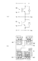
各パワー半導体モジュール1U~1Wの等価回路は、図9(a)に示すように、主端子を構成する正極側接続端子11と主端子を構成する負極側接続端子13との間に、上アームを構成する逆導通IGBTQUと下アームを構成する逆導通IGBTQLとが直列に接続された構成を有する。
このため、例えば下アームの逆導通IGBTQLのゲート電極4gに低レベルのゲート電圧を供給してオフ状態としている状態で、上アームの逆導通IGBTQUのゲート電極4gにオン・オフを繰り返すゲート電圧を加えてスイッチング状態とする。この場合には、逆導通IGBTQUがターンオンした時点で図9(a)に示すように正極側接続端子11から逆導通IGBTQUに向かう電流が流れる。このため、図9(b)に示すハッチング図示の正極側接続端子11に電流が流れる。
各パワー半導体モジュール1U~1Wの等価回路は、図9(a)に示すように、主端子を構成する正極側接続端子11と主端子を構成する負極側接続端子13との間に、上アームを構成する逆導通IGBTQUと下アームを構成する逆導通IGBTQLとが直列に接続された構成を有する。
このため、例えば下アームの逆導通IGBTQLのゲート電極4gに低レベルのゲート電圧を供給してオフ状態としている状態で、上アームの逆導通IGBTQUのゲート電極4gにオン・オフを繰り返すゲート電圧を加えてスイッチング状態とする。この場合には、逆導通IGBTQUがターンオンした時点で図9(a)に示すように正極側接続端子11から逆導通IGBTQUに向かう電流が流れる。このため、図9(b)に示すハッチング図示の正極側接続端子11に電流が流れる。
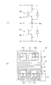
この正極側接続端子11からの電流は、図10(a)及び(b)に示すように、上アーム用絶縁基板3Uの上アーム用配線パターン部3dを通じて各上アーム用半導体チップ4U1及び4U2に内蔵された逆導通IGBTのコレクタ電極に入力される。
そして、逆導通IGBTのコレクタ電極を通じてエミッタ電極から図11(a)及び(b)に示すように出力される。このエミッタ電極から出力された電流は、図11(b)に示すように、上アーム配線用導体板5Uのチップ対向板部5U1及び5U2を通じ、さらに接続板部5U3を通じて下アーム用絶縁基板3Lの下アーム用配線パターン部3eの接続部3e2に供給される。
そして、逆導通IGBTのコレクタ電極を通じてエミッタ電極から図11(a)及び(b)に示すように出力される。このエミッタ電極から出力された電流は、図11(b)に示すように、上アーム配線用導体板5Uのチップ対向板部5U1及び5U2を通じ、さらに接続板部5U3を通じて下アーム用絶縁基板3Lの下アーム用配線パターン部3eの接続部3e2に供給される。
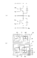
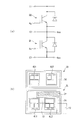
この接続部3e2に供給された電流は、図12(a)及び(b)に示すように、下アーム用配線パターン部3eを通って、図13(a)及び(b)に示すように出力端子12から出力される。
逆に、上アームを構成する逆導通IGBTQUのゲート電極4gに低レベルのゲート電圧を印加してこの逆導通IGBTQUをオフ状態とした状態で、下アームを構成する逆導通IGBTQLのゲート電極4gにオン・オフを繰り返すゲート電圧を印加してスイッチング状態とする。この場合には、逆導通IGBTQLがターンオンしたときに、出力端子12から入力される電流が、図14(a)及び(b)に示すように、下アーム用絶縁基板3Lの下アーム用配線パターン部3eを通じて下アームを構成する逆導通IGBTQLのコレクタ電極に入力される。
逆に、上アームを構成する逆導通IGBTQUのゲート電極4gに低レベルのゲート電圧を印加してこの逆導通IGBTQUをオフ状態とした状態で、下アームを構成する逆導通IGBTQLのゲート電極4gにオン・オフを繰り返すゲート電圧を印加してスイッチング状態とする。この場合には、逆導通IGBTQLがターンオンしたときに、出力端子12から入力される電流が、図14(a)及び(b)に示すように、下アーム用絶縁基板3Lの下アーム用配線パターン部3eを通じて下アームを構成する逆導通IGBTQLのコレクタ電極に入力される。
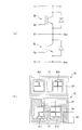
逆導通IGBTQLのコレクタに入力された電流は上部のエミッタ電極4Leから出力され、図15(a)及び(b)に示すように、下アーム配線用導体板5Lを通じ、図16(a)及び(b)に示すように下アーム用絶縁基板3Lに形成された接地用配線パターン部3fを通じて、図17(a)及び(b)に示すように負極側接続端子13に流れ、この負極側接続端子13から電源の負極側に戻る。
このようにして、上アーム及び下アームを構成する逆導通IGBTによって三相交流の一相分が形成される。このため、3つのパワー半導体モジュール1U~1Wを120度ずれたゲート信号でオン・オフ制御することにより、U相、V相及びW相の3相交流を負荷に出力することができる。
このようにして、上アーム及び下アームを構成する逆導通IGBTによって三相交流の一相分が形成される。このため、3つのパワー半導体モジュール1U~1Wを120度ずれたゲート信号でオン・オフ制御することにより、U相、V相及びW相の3相交流を負荷に出力することができる。
このように、各パワー半導体モジュール1U~1Wが動作状態となると、各逆導通IGBTQU及びQLを内蔵した半導体チップ4U1,4U2及び4L1,4L2が発熱状態となる。
これら各半導体チップ4U1,4U2及び4L1,4L2の発熱は、図2に示すように、上アーム用配線パターン部3d及び下アーム用配線パターン部3eを通じ、絶縁板部3aを通じ、さらに放熱用銅板部3cを通じ、金属微粒子を焼結した金属焼結材20を通じて冷却体21の蓋体26に熱伝導される。
そして、蓋体26に伝熱された熱は冷却水に接触する冷却フィン27で冷却される。
これら各半導体チップ4U1,4U2及び4L1,4L2の発熱は、図2に示すように、上アーム用配線パターン部3d及び下アーム用配線パターン部3eを通じ、絶縁板部3aを通じ、さらに放熱用銅板部3cを通じ、金属微粒子を焼結した金属焼結材20を通じて冷却体21の蓋体26に熱伝導される。
そして、蓋体26に伝熱された熱は冷却水に接触する冷却フィン27で冷却される。
このとき、発熱する各半導体チップ4U1,4U2及び4L1,4L2を実装する上アーム用絶縁基板3U及び下アーム用絶縁基板3Lは、比較的厚みの薄い絶縁板部3aと絶縁板部3aの表裏に形成された配線パターン用銅板部3b及び放熱用銅板部3cにより構成されている。上アーム用配線パターン部3d及び下アーム用配線パターン部3eを構成する配線パターン用銅板部3bと放熱用銅板部3cの厚みが0.7mm以上で好ましくは1mm以上に形成されているので、前述したように、熱応力を緩和するとともに、熱抵抗を抑制して熱伝導効率を向上させることができる。
しかも、上アーム用絶縁基板3U及び下アーム用絶縁基板3Lの放熱用銅板部3cがそれぞれ金属微粒子を例えば10MPaで加圧した状態で、250℃に加熱して有機溶剤を蒸発させて金属微粒子同士を焼結する加圧・加熱接合するので、この接合部での厚みを薄くしながら接合強度を確保するとともに、熱伝導率を高くすることができる。
しかも、上アーム用絶縁基板3U及び下アーム用絶縁基板3Lの放熱用銅板部3cがそれぞれ金属微粒子を例えば10MPaで加圧した状態で、250℃に加熱して有機溶剤を蒸発させて金属微粒子同士を焼結する加圧・加熱接合するので、この接合部での厚みを薄くしながら接合強度を確保するとともに、熱伝導率を高くすることができる。
したがって、各半導体チップ4U1,4U2及び4L1,4L2の発熱を高熱伝導効率で冷却体21に伝熱することができ、冷却体21で良好な冷却を行うことができ、各半導体チップ4U1,4U2及び4L1,4L2が過熱状態となることを確実に防止することができる。
また、半導体チップ4U1,4U2及び4L1,4L2に内蔵するスイッチング素子として逆導通IGBTQU及びQLを適用することにより、IGBT及びFWDを個別の半導体チップに内蔵させる場合に比較してチップ面積を50%程度縮小することができ、この分パワー半導体モジュール1U~1Wを小型化することができる。
また、半導体チップ4U1,4U2及び4L1,4L2に内蔵するスイッチング素子として逆導通IGBTQU及びQLを適用することにより、IGBT及びFWDを個別の半導体チップに内蔵させる場合に比較してチップ面積を50%程度縮小することができ、この分パワー半導体モジュール1U~1Wを小型化することができる。
さらに、上記実施形態では、半導体チップ4U1,4U2及び4L1,4L2と外部接続端子となる正極側接続端子11、出力端子12及び負極側接続端子13との間の電流路が、細いボンディングワイヤを使用することなく、棒状の導電ポスト5Up及び5Lpをそれぞれ備える上アーム配線用導体板5U及び下アーム配線用導体板5Lと、銅板で構成される上アーム用配線パターン部3d、下アーム用配線パターン部3e及び接地用配線パターン部3fとで構成されているので、配線インダクタンスはボンディングワイヤを使用した場合の20~40nHから1~2nH程度に小さくすることができる。このため、スイッチング速度を向上させることができる。また、半導体チップ4U1,4U2及び4L1,4L2の制御端子と外部接続用制御端子19との接続でもボンディングワイヤを使用することなくリードフレーム18を使用して接続するので、発生するジュール熱をボンディングワイヤに比較して小さくすることができる。
次に、本発明の第2の実施形態について図18及び図19を伴って説明する。
この第2の実施形態では、冷却体21の構成を一体型に変更したものである。
すなわち、第2の実施形態では、図18及び図19に示すように、冷却体21をケース体22と蓋体26に分割することなく、ケース体22の冷却水通路25に直接冷却フィンに相当する隔壁31を幅方向に所定間隔を保って多数形成した構成としている。
そして、ケース体22の上面に前述した第1の実施形態と同様の構成を有するパワー半導体モジュール1U~1WをAg等の金属微粒子を加圧・加熱して焼結した接合部材で接合している。
この第2の実施形態では、冷却体21の構成を一体型に変更したものである。
すなわち、第2の実施形態では、図18及び図19に示すように、冷却体21をケース体22と蓋体26に分割することなく、ケース体22の冷却水通路25に直接冷却フィンに相当する隔壁31を幅方向に所定間隔を保って多数形成した構成としている。
そして、ケース体22の上面に前述した第1の実施形態と同様の構成を有するパワー半導体モジュール1U~1WをAg等の金属微粒子を加圧・加熱して焼結した接合部材で接合している。
この第2の実施形態においても、冷却体21にパワー半導体モジュール1U~1Wを、金属微粒子を焼結した接合部材で接合するようにしているので、この接合部材での熱伝導率を高めることができるとともに、強固な接合を得ることができる。
しかも、冷却体21に開口部が存在しない一体構造であるので、冷却水等の冷却媒体が外部に漏れることを確実に回避することができる。
なお、上記実施形態においては、2in1タイプの半導体モジュール1U~1Wを適用した場合について説明したが、これに限定されるものではなく1in1タイプ、4in1タイプ、6in1タイプ等の種々のタイプのパワー半導体モジュールに本発明を適用することができる。
しかも、冷却体21に開口部が存在しない一体構造であるので、冷却水等の冷却媒体が外部に漏れることを確実に回避することができる。
なお、上記実施形態においては、2in1タイプの半導体モジュール1U~1Wを適用した場合について説明したが、これに限定されるものではなく1in1タイプ、4in1タイプ、6in1タイプ等の種々のタイプのパワー半導体モジュールに本発明を適用することができる。
また、各アームを構成する半導体チップ数も2つに限らず、使用する電流量に応じて並列に配置する半導体チップ数を任意に設定することかできる。これに応じて導電ポスト数も使用電流に応じて任意数に設定することができる。
さらに、上記実施形態においては、冷却体21上に3つのパワー半導体モジュール1U~1Wを載置した場合について説明したが、これに限定されるものではなく、用途に応じて任意数のパワー半導体モジュールを載置することができる。
また、上記実施形態では、半導体チップ4U1,4U2及び4L1,4L2に内蔵するスイッチング素子として逆導通IGBTQU及びQLを適用した場合について説明したが、これに限定されるものではなく、IGBTを内蔵した半導体チップとFWDを内蔵した半導体チップを逆並列に接続するようにしても良く、IGBTに代えてパワーMOSFET(Metal-Oxide-Semiconductor Field-Effect Transistor)等の他の電圧制御型スイッチング素子を適用することができる。
さらに、上記実施形態においては、冷却体21上に3つのパワー半導体モジュール1U~1Wを載置した場合について説明したが、これに限定されるものではなく、用途に応じて任意数のパワー半導体モジュールを載置することができる。
また、上記実施形態では、半導体チップ4U1,4U2及び4L1,4L2に内蔵するスイッチング素子として逆導通IGBTQU及びQLを適用した場合について説明したが、これに限定されるものではなく、IGBTを内蔵した半導体チップとFWDを内蔵した半導体チップを逆並列に接続するようにしても良く、IGBTに代えてパワーMOSFET(Metal-Oxide-Semiconductor Field-Effect Transistor)等の他の電圧制御型スイッチング素子を適用することができる。
さらに、上記実施形態においては、上アーム用の絶縁基板3U及び下アーム用の絶縁基板3L、半導体チップ4U1,4U2,4L1,4L2、上アーム用の配線用導体板5U及び下アーム用の配線用導体板5Lを絶縁樹脂封止部材6でモールド成型した場合について説明したが、これに限定されるものではなく、上アーム用の絶縁基板3U及び下アーム用の絶縁基板3L、半導体チップ4U1,4U2,4L1,4L2、上アーム用の配線用導体板5U及び下アーム用の配線用導体板5Lをケースで覆い、ケース内部にゲル状封止部材を充填するようにしてもよい。
また、上記実施形態においては、絶縁基板3U及び3Lを設けた場合について説明したが、これに限定されるものではなく、絶縁基板を構成する部材と封止材の線膨張係数差が問題にならない場合などでは、一枚の絶縁板部に上アーム用配線パターン部3d及び下アーム用配線パターン部3e、接地用配線パターン部3fの複数の配線パターンを備える配線パターン用銅板部を形成すると共に、共通の放熱用伝熱パターン(放熱用銅板部)3cを形成するようにしてもよい。
また、上記実施形態においては、絶縁基板3U及び3Lを設けた場合について説明したが、これに限定されるものではなく、絶縁基板を構成する部材と封止材の線膨張係数差が問題にならない場合などでは、一枚の絶縁板部に上アーム用配線パターン部3d及び下アーム用配線パターン部3e、接地用配線パターン部3fの複数の配線パターンを備える配線パターン用銅板部を形成すると共に、共通の放熱用伝熱パターン(放熱用銅板部)3cを形成するようにしてもよい。
また、上記実施形態においては絶縁基板3U,3Lの絶縁板部3aとしては、アルミナ(Al2O3)、窒化アルミニウム(AlN)等のセラミック基材を適用することができる。
また、上記実施形態においては、円柱状の導電ポスト5Up及び5Lpを適用する場合について説明したが、これに限定されるものではなく、四角柱、三角柱、多角柱、楕円柱等の任意の形状の導電ポストを適用することができる。要は導電ポスト5Up及び5Lpは、インダクタンスの減少に寄与する導電棒状体であれば良い。また、銅板で構成された上アーム配線用導体板5U及び下アーム配線用導体板5Lに代えてプリント基板を適用することもできる。
また、本発明は、パワー半導体モジュールの端子接続の組み合わせだけで所望する回路構成が得られることから、本発明は上述した電力変換用インバータ装置に限定されるものではなく、パワー半導体モジュールを使用する他の電力変換装置や高周波用途のスイッチングIC等の他の半導体装置に本発明を適用することができる。
また、上記実施形態においては、円柱状の導電ポスト5Up及び5Lpを適用する場合について説明したが、これに限定されるものではなく、四角柱、三角柱、多角柱、楕円柱等の任意の形状の導電ポストを適用することができる。要は導電ポスト5Up及び5Lpは、インダクタンスの減少に寄与する導電棒状体であれば良い。また、銅板で構成された上アーム配線用導体板5U及び下アーム配線用導体板5Lに代えてプリント基板を適用することもできる。
また、本発明は、パワー半導体モジュールの端子接続の組み合わせだけで所望する回路構成が得られることから、本発明は上述した電力変換用インバータ装置に限定されるものではなく、パワー半導体モジュールを使用する他の電力変換装置や高周波用途のスイッチングIC等の他の半導体装置に本発明を適用することができる。
1U~1W…パワー半導体モジュール、3U…上アーム用絶縁基板、3L…下アーム用絶縁基板、3a…絶縁板部、3b…配線パターン用銅板部、3c…放熱用銅板部、3d…上アーム用配線パターン部、3e…下アーム用配線パターン部、3f…接地用配線パターン部、4U,4U1,4U2…上アーム用半導体チップ、4L,4L1,4L2…下アーム用半導体チップ、5U…上アーム配線用導体板、5L…下アーム配線用導体板、5Up,5Lp…導電ポスト、6…絶縁樹脂封止部材、11…正極側接続端子、12…出力端子、13…負極側接続端子、17…外部接続補助端子、20…金属焼結材、21…冷却体、22…ケース体、23…注入口、24…排出口、25…冷却水通路、26…蓋体、27…冷却フィン
Claims (9)
- 絶縁板部の一方に配線パターンを形成する配線パターン用銅板部を配置し、他方に放熱用銅板部を配置した絶縁基板と、
該絶縁基板の前記配線パターン用銅板部に実装された半導体チップと、
前記絶縁基板の放熱用銅板部に接合された冷却体と、
前記半導体チップと前記配線パターン用銅板部とに接続された配線用導体板とを備え、
前記絶縁基板の放熱用銅板部と前記冷却体とを金属焼結材で接合するとともに、前記配線パターン用銅板部及び前記放熱用銅板部の厚みが熱応力を緩和する厚みに設定されている
ことを特徴とする半導体装置。 - 前記配線パターン用銅板部及び前記放熱用銅板部の厚みが熱応力を緩和し、且つ熱抵抗を抑制する厚みに設定されていることを特徴とする請求項1に記載の半導体装置。
- 前記配線用導体板と前記半導体チップ及び前記配線パターン用銅板部との電気的接続は導電性棒状体を介して行われていることを特徴とする請求項1又は2に記載の半導体装置。
- 前記導電性棒状体は、前記半導体チップ及び配線パターン用銅板部と前記配線用導体板との間の棒部の断面積に比較して前記配線用導体板に嵌合する嵌合部の断面積が広く設定されていることを特徴とする請求項3に記載の半導体装置。
- 前記半導体チップは、絶縁ゲートバイポーラトランジスタとこれに逆接続したフリー・ホイーリング・ダイオードとをワンチップ化して構成されていることを特徴とする請求項1又は2に記載の半導体装置。
- 前記配線パターン用銅板部及び前記放熱用銅板部の厚みが0.7mm以上に設定されていることを特徴とする請求項2に記載の半導体装置。
- 前記絶縁基板の配線パターン用銅板部は、上アームを構成する半導体チップを実装する上アーム用配線パターン部と、下アームを構成する半導体チップを実装する下アーム用配線パターン部と、接地用配線パターン部とが互いに独立して前記絶縁板部上に形成されていることを特徴とする請求項1又は2に記載の半導体装置。
- 前記上アーム用配線パターン部に正極側接続端子が接続され、前記下アーム用配線パターン部に出力端子が接続され、前記接地用配線パターン部に負極側接続端子が接続されていることを特徴とする請求項7に記載の半導体装置。
- 前記配線用導体板は、前記上アームを構成する半導体チップと前記下アーム用配線パターン部とを接続する第1の配線用導体板部と、前記下アームを構成する半導体チップと前記接地用配線パターン部とを接続する第2の配線用導体板部とで構成されていることを特徴とする請求項7に記載の半導体装置。
Priority Applications (2)
| Application Number | Priority Date | Filing Date | Title |
|---|---|---|---|
| JP2015513575A JP6176320B2 (ja) | 2013-04-25 | 2014-04-25 | 半導体装置 |
| US14/850,196 US9673129B2 (en) | 2013-04-25 | 2015-09-10 | Semiconductor device |
Applications Claiming Priority (2)
| Application Number | Priority Date | Filing Date | Title |
|---|---|---|---|
| JP2013092796 | 2013-04-25 | ||
| JP2013-092796 | 2013-04-25 |
Related Child Applications (1)
| Application Number | Title | Priority Date | Filing Date |
|---|---|---|---|
| US14/850,196 Continuation US9673129B2 (en) | 2013-04-25 | 2015-09-10 | Semiconductor device |
Publications (1)
| Publication Number | Publication Date |
|---|---|
| WO2014174854A1 true WO2014174854A1 (ja) | 2014-10-30 |
Family
ID=51791442
Family Applications (1)
| Application Number | Title | Priority Date | Filing Date |
|---|---|---|---|
| PCT/JP2014/002347 Ceased WO2014174854A1 (ja) | 2013-04-25 | 2014-04-25 | 半導体装置 |
Country Status (3)
| Country | Link |
|---|---|
| US (1) | US9673129B2 (ja) |
| JP (1) | JP6176320B2 (ja) |
| WO (1) | WO2014174854A1 (ja) |
Cited By (5)
| Publication number | Priority date | Publication date | Assignee | Title |
|---|---|---|---|---|
| US9999146B2 (en) | 2015-12-17 | 2018-06-12 | Fuji Electric Co., Ltd. | Semiconductor module |
| WO2018155216A1 (ja) * | 2017-02-24 | 2018-08-30 | 富士電機株式会社 | 評価方法、推定方法、評価装置、および複合評価装置 |
| JP6644196B1 (ja) * | 2019-02-01 | 2020-02-12 | 三菱電機株式会社 | 半導体装置およびその製造方法ならびに電力変換装置 |
| JP2022524961A (ja) * | 2019-02-28 | 2022-05-11 | ヒタチ・エナジー・スウィツァーランド・アクチェンゲゼルシャフト | 冷却器フレームの一体化が向上した電力変換装置 |
| WO2024225129A1 (ja) * | 2023-04-28 | 2024-10-31 | 新電元工業株式会社 | 電子モジュール |
Families Citing this family (14)
| Publication number | Priority date | Publication date | Assignee | Title |
|---|---|---|---|---|
| CN103814439B (zh) * | 2011-09-09 | 2016-10-19 | 株式会社村田制作所 | 模块基板 |
| US9725367B2 (en) * | 2013-03-29 | 2017-08-08 | Mitsubishi Materials Corporation | Apparatus and method for producing (metal plate)-(ceramic board) laminated assembly, and apparatus and method for producing power-module substrate |
| CN106415834B (zh) * | 2014-11-28 | 2019-09-13 | 富士电机株式会社 | 半导体装置 |
| JP6578795B2 (ja) * | 2015-08-04 | 2019-09-25 | 富士電機株式会社 | 半導体装置及び半導体装置の製造方法 |
| CN107240581A (zh) * | 2016-03-29 | 2017-10-10 | 株式会社京浜 | 电力转换装置及电力转换装置的制造方法 |
| US10900412B2 (en) * | 2018-05-31 | 2021-01-26 | Borg Warner Inc. | Electronics assembly having a heat sink and an electrical insulator directly bonded to the heat sink |
| US11129310B2 (en) * | 2018-11-22 | 2021-09-21 | Fuji Electric Co., Ltd. | Semiconductor module, vehicle and manufacturing method |
| CN112913009B (zh) * | 2019-04-10 | 2024-08-16 | 新电元工业株式会社 | 半导体装置以及引线框材料 |
| CN113892172B (zh) * | 2019-05-30 | 2025-01-14 | 三菱电机株式会社 | 半导体装置 |
| WO2021001924A1 (ja) * | 2019-07-02 | 2021-01-07 | 三菱電機株式会社 | パワーモジュールおよびその製造方法 |
| JP7413720B2 (ja) * | 2019-10-28 | 2024-01-16 | 富士電機株式会社 | 半導体モジュール |
| JP1669329S (ja) * | 2020-03-13 | 2020-10-05 | ||
| USD949808S1 (en) * | 2020-11-27 | 2022-04-26 | Sansha Electric Manufacturing Co., Ltd. | Semiconductor device |
| EP4266363A1 (en) * | 2022-04-21 | 2023-10-25 | Airbus SAS | Improved power component for electric or hybrid aircraft |
Citations (4)
| Publication number | Priority date | Publication date | Assignee | Title |
|---|---|---|---|---|
| JPH08335652A (ja) * | 1995-06-09 | 1996-12-17 | Mitsubishi Materials Corp | パワーモジュール用基板及びその製造方法 |
| JP2003116282A (ja) * | 2001-10-09 | 2003-04-18 | Hitachi Ltd | 水冷インバータ |
| JP2003243610A (ja) * | 2002-02-19 | 2003-08-29 | Hitachi Ltd | 絶縁型半導体装置 |
| JP2008086099A (ja) * | 2006-09-27 | 2008-04-10 | Honda Motor Co Ltd | インバータ装置 |
Family Cites Families (8)
| Publication number | Priority date | Publication date | Assignee | Title |
|---|---|---|---|---|
| US6245442B1 (en) * | 1997-05-28 | 2001-06-12 | Kabushiki Kaisha Toyota Chuo | Metal matrix composite casting and manufacturing method thereof |
| JP4207896B2 (ja) * | 2005-01-19 | 2009-01-14 | 富士電機デバイステクノロジー株式会社 | 半導体装置 |
| JP2006202938A (ja) * | 2005-01-20 | 2006-08-03 | Kojiro Kobayashi | 半導体装置及びその製造方法 |
| JP5028085B2 (ja) * | 2006-12-27 | 2012-09-19 | アイシン・エィ・ダブリュ株式会社 | 電子回路装置とその製造方法 |
| WO2009125779A1 (ja) * | 2008-04-09 | 2009-10-15 | 富士電機デバイステクノロジー株式会社 | 半導体装置及び半導体装置の製造方法 |
| JP5707896B2 (ja) | 2010-11-24 | 2015-04-30 | 三菱マテリアル株式会社 | ヒートシンク付パワーモジュール用基板、パワーモジュール及びパワーモジュール用基板の製造方法 |
| JP5732880B2 (ja) * | 2011-02-08 | 2015-06-10 | 株式会社デンソー | 半導体装置及びその製造方法 |
| JP5807348B2 (ja) * | 2011-03-10 | 2015-11-10 | 富士電機株式会社 | 半導体装置およびその製造方法 |
-
2014
- 2014-04-25 WO PCT/JP2014/002347 patent/WO2014174854A1/ja not_active Ceased
- 2014-04-25 JP JP2015513575A patent/JP6176320B2/ja active Active
-
2015
- 2015-09-10 US US14/850,196 patent/US9673129B2/en active Active
Patent Citations (4)
| Publication number | Priority date | Publication date | Assignee | Title |
|---|---|---|---|---|
| JPH08335652A (ja) * | 1995-06-09 | 1996-12-17 | Mitsubishi Materials Corp | パワーモジュール用基板及びその製造方法 |
| JP2003116282A (ja) * | 2001-10-09 | 2003-04-18 | Hitachi Ltd | 水冷インバータ |
| JP2003243610A (ja) * | 2002-02-19 | 2003-08-29 | Hitachi Ltd | 絶縁型半導体装置 |
| JP2008086099A (ja) * | 2006-09-27 | 2008-04-10 | Honda Motor Co Ltd | インバータ装置 |
Cited By (10)
| Publication number | Priority date | Publication date | Assignee | Title |
|---|---|---|---|---|
| US9999146B2 (en) | 2015-12-17 | 2018-06-12 | Fuji Electric Co., Ltd. | Semiconductor module |
| WO2018155216A1 (ja) * | 2017-02-24 | 2018-08-30 | 富士電機株式会社 | 評価方法、推定方法、評価装置、および複合評価装置 |
| CN109564259A (zh) * | 2017-02-24 | 2019-04-02 | 富士电机株式会社 | 评价方法、推定方法、评价装置及综合评价装置 |
| US11143691B2 (en) | 2017-02-24 | 2021-10-12 | Fuji Electric Co., Ltd. | Evaluation method, estimation method, evaluation apparatus, and combined evaluation apparatus |
| JP6644196B1 (ja) * | 2019-02-01 | 2020-02-12 | 三菱電機株式会社 | 半導体装置およびその製造方法ならびに電力変換装置 |
| WO2020157965A1 (ja) * | 2019-02-01 | 2020-08-06 | 三菱電機株式会社 | 半導体装置およびその製造方法ならびに電力変換装置 |
| US12308304B2 (en) | 2019-02-01 | 2025-05-20 | Mitsubishi Electric Corporation | Semiconductor device and method of manufacturing the same, and power conversion device |
| JP2022524961A (ja) * | 2019-02-28 | 2022-05-11 | ヒタチ・エナジー・スウィツァーランド・アクチェンゲゼルシャフト | 冷却器フレームの一体化が向上した電力変換装置 |
| JP7573818B2 (ja) | 2019-02-28 | 2024-10-28 | ヒタチ・エナジー・リミテッド | 冷却器フレームの一体化が向上した電力変換装置 |
| WO2024225129A1 (ja) * | 2023-04-28 | 2024-10-31 | 新電元工業株式会社 | 電子モジュール |
Also Published As
| Publication number | Publication date |
|---|---|
| US9673129B2 (en) | 2017-06-06 |
| JPWO2014174854A1 (ja) | 2017-02-23 |
| JP6176320B2 (ja) | 2017-08-09 |
| US20150380338A1 (en) | 2015-12-31 |
Similar Documents
| Publication | Publication Date | Title |
|---|---|---|
| JP6176320B2 (ja) | 半導体装置 | |
| CN111916411B (zh) | 对用电器进行可控的电功率供应的功率模块 | |
| JP6065995B2 (ja) | 半導体装置及び半導体装置の製造方法 | |
| US8872332B2 (en) | Power module with directly attached thermally conductive structures | |
| CN104637910B (zh) | 半导体模块和其制造方法 | |
| CN106952897B (zh) | 半导体装置及其制造方法 | |
| KR101388737B1 (ko) | 반도체 패키지, 반도체 모듈, 및 그 실장 구조 | |
| US9385107B2 (en) | Multichip device including a substrate | |
| JP2014199829A (ja) | 半導体モジュール及びそれを搭載したインバータ | |
| US9579746B2 (en) | Thermocompression bonding structure and thermocompression bonding method | |
| CN104134636A (zh) | 用于半导体模块的直接冷却衬底和相应的制造方法 | |
| CN104517939A (zh) | 垂直分流电阻 | |
| CN116666322A (zh) | 半导体封装件、冷却系统、基板以及该基板制造方法 | |
| JP2017022346A (ja) | 半導体装置及び半導体装置の製造方法 | |
| JP2018110218A (ja) | 半導体装置およびその製造方法 | |
| CN111354710B (zh) | 半导体装置及其制造方法 | |
| WO2013171946A1 (ja) | 半導体装置の製造方法および半導体装置 | |
| WO2005119896A1 (ja) | インバータ装置 | |
| JP5987635B2 (ja) | パワー半導体モジュール | |
| US9698076B1 (en) | Metal slugs for double-sided cooling of power module | |
| CN107124837B (zh) | 电子模块及制造其的方法 | |
| JP5682511B2 (ja) | 半導体モジュール | |
| JP2011176087A (ja) | 半導体モジュール、及び電力変換装置 | |
| JP2016001644A (ja) | 半導体モジュール | |
| JP2014116478A (ja) | 半導体モジュール及び半導体モジュールの製造方法並びに電力変換装置 |
Legal Events
| Date | Code | Title | Description |
|---|---|---|---|
| 121 | Ep: the epo has been informed by wipo that ep was designated in this application |
Ref document number: 14788743 Country of ref document: EP Kind code of ref document: A1 |
|
| ENP | Entry into the national phase |
Ref document number: 2015513575 Country of ref document: JP Kind code of ref document: A |
|
| NENP | Non-entry into the national phase |
Ref country code: DE |
|
| 122 | Ep: pct application non-entry in european phase |
Ref document number: 14788743 Country of ref document: EP Kind code of ref document: A1 |