WO2014157303A1 - 導電膜形成用組成物およびこれを用いる導電膜の製造方法 - Google Patents
導電膜形成用組成物およびこれを用いる導電膜の製造方法 Download PDFInfo
- Publication number
- WO2014157303A1 WO2014157303A1 PCT/JP2014/058455 JP2014058455W WO2014157303A1 WO 2014157303 A1 WO2014157303 A1 WO 2014157303A1 JP 2014058455 W JP2014058455 W JP 2014058455W WO 2014157303 A1 WO2014157303 A1 WO 2014157303A1
- Authority
- WO
- WIPO (PCT)
- Prior art keywords
- conductive film
- copper
- composition
- forming
- complex
- Prior art date
- Legal status (The legal status is an assumption and is not a legal conclusion. Google has not performed a legal analysis and makes no representation as to the accuracy of the status listed.)
- Ceased
Links
- 0 *C(C(*)(*)N(*)*)O* Chemical compound *C(C(*)(*)N(*)*)O* 0.000 description 1
Classifications
-
- C—CHEMISTRY; METALLURGY
- C09—DYES; PAINTS; POLISHES; NATURAL RESINS; ADHESIVES; COMPOSITIONS NOT OTHERWISE PROVIDED FOR; APPLICATIONS OF MATERIALS NOT OTHERWISE PROVIDED FOR
- C09D—COATING COMPOSITIONS, e.g. PAINTS, VARNISHES OR LACQUERS; FILLING PASTES; CHEMICAL PAINT OR INK REMOVERS; INKS; CORRECTING FLUIDS; WOODSTAINS; PASTES OR SOLIDS FOR COLOURING OR PRINTING; USE OF MATERIALS THEREFOR
- C09D5/00—Coating compositions, e.g. paints, varnishes or lacquers, characterised by their physical nature or the effects produced; Filling pastes
- C09D5/24—Electrically-conducting paints
-
- C—CHEMISTRY; METALLURGY
- C09—DYES; PAINTS; POLISHES; NATURAL RESINS; ADHESIVES; COMPOSITIONS NOT OTHERWISE PROVIDED FOR; APPLICATIONS OF MATERIALS NOT OTHERWISE PROVIDED FOR
- C09D—COATING COMPOSITIONS, e.g. PAINTS, VARNISHES OR LACQUERS; FILLING PASTES; CHEMICAL PAINT OR INK REMOVERS; INKS; CORRECTING FLUIDS; WOODSTAINS; PASTES OR SOLIDS FOR COLOURING OR PRINTING; USE OF MATERIALS THEREFOR
- C09D129/00—Coating compositions based on homopolymers or copolymers of compounds having one or more unsaturated aliphatic radicals, each having only one carbon-to-carbon double bond, and at least one being terminated by an alcohol, ether, aldehydo, ketonic, acetal, or ketal radical; Coating compositions based on hydrolysed polymers of esters of unsaturated alcohols with saturated carboxylic acids; Coating compositions based on derivatives of such polymers
- C09D129/02—Homopolymers or copolymers of unsaturated alcohols
- C09D129/04—Polyvinyl alcohol; Partially hydrolysed homopolymers or copolymers of esters of unsaturated alcohols with saturated carboxylic acids
-
- C—CHEMISTRY; METALLURGY
- C09—DYES; PAINTS; POLISHES; NATURAL RESINS; ADHESIVES; COMPOSITIONS NOT OTHERWISE PROVIDED FOR; APPLICATIONS OF MATERIALS NOT OTHERWISE PROVIDED FOR
- C09D—COATING COMPOSITIONS, e.g. PAINTS, VARNISHES OR LACQUERS; FILLING PASTES; CHEMICAL PAINT OR INK REMOVERS; INKS; CORRECTING FLUIDS; WOODSTAINS; PASTES OR SOLIDS FOR COLOURING OR PRINTING; USE OF MATERIALS THEREFOR
- C09D139/00—Coating compositions based on homopolymers or copolymers of compounds having one or more unsaturated aliphatic radicals, each having only one carbon-to-carbon double bond, and at least one being terminated by a single or double bond to nitrogen or by a heterocyclic ring containing nitrogen; Coating compositions based on derivatives of such polymers
- C09D139/04—Homopolymers or copolymers of monomers containing heterocyclic rings having nitrogen as ring member
- C09D139/06—Homopolymers or copolymers of N-vinyl-pyrrolidones
-
- C—CHEMISTRY; METALLURGY
- C09—DYES; PAINTS; POLISHES; NATURAL RESINS; ADHESIVES; COMPOSITIONS NOT OTHERWISE PROVIDED FOR; APPLICATIONS OF MATERIALS NOT OTHERWISE PROVIDED FOR
- C09D—COATING COMPOSITIONS, e.g. PAINTS, VARNISHES OR LACQUERS; FILLING PASTES; CHEMICAL PAINT OR INK REMOVERS; INKS; CORRECTING FLUIDS; WOODSTAINS; PASTES OR SOLIDS FOR COLOURING OR PRINTING; USE OF MATERIALS THEREFOR
- C09D171/00—Coating compositions based on polyethers obtained by reactions forming an ether link in the main chain; Coating compositions based on derivatives of such polymers
- C09D171/02—Polyalkylene oxides
-
- C—CHEMISTRY; METALLURGY
- C09—DYES; PAINTS; POLISHES; NATURAL RESINS; ADHESIVES; COMPOSITIONS NOT OTHERWISE PROVIDED FOR; APPLICATIONS OF MATERIALS NOT OTHERWISE PROVIDED FOR
- C09D—COATING COMPOSITIONS, e.g. PAINTS, VARNISHES OR LACQUERS; FILLING PASTES; CHEMICAL PAINT OR INK REMOVERS; INKS; CORRECTING FLUIDS; WOODSTAINS; PASTES OR SOLIDS FOR COLOURING OR PRINTING; USE OF MATERIALS THEREFOR
- C09D7/00—Features of coating compositions, not provided for in group C09D5/00; Processes for incorporating ingredients in coating compositions
- C09D7/40—Additives
- C09D7/60—Additives non-macromolecular
- C09D7/61—Additives non-macromolecular inorganic
-
- H—ELECTRICITY
- H05—ELECTRIC TECHNIQUES NOT OTHERWISE PROVIDED FOR
- H05K—PRINTED CIRCUITS; CASINGS OR CONSTRUCTIONAL DETAILS OF ELECTRIC APPARATUS; MANUFACTURE OF ASSEMBLAGES OF ELECTRICAL COMPONENTS
- H05K1/00—Printed circuits
- H05K1/02—Details
- H05K1/09—Use of materials for the conductive, e.g. metallic pattern
- H05K1/092—Dispersed materials, e.g. conductive pastes or inks
- H05K1/095—Dispersed materials, e.g. conductive pastes or inks for polymer thick films, i.e. having a permanent organic polymeric binder
-
- C—CHEMISTRY; METALLURGY
- C08—ORGANIC MACROMOLECULAR COMPOUNDS; THEIR PREPARATION OR CHEMICAL WORKING-UP; COMPOSITIONS BASED THEREON
- C08K—Use of inorganic or non-macromolecular organic substances as compounding ingredients
- C08K3/00—Use of inorganic substances as compounding ingredients
- C08K3/18—Oxygen-containing compounds, e.g. metal carbonyls
- C08K3/20—Oxides; Hydroxides
- C08K3/22—Oxides; Hydroxides of metals
- C08K2003/2248—Oxides; Hydroxides of metals of copper
-
- C—CHEMISTRY; METALLURGY
- C08—ORGANIC MACROMOLECULAR COMPOUNDS; THEIR PREPARATION OR CHEMICAL WORKING-UP; COMPOSITIONS BASED THEREON
- C08L—COMPOSITIONS OF MACROMOLECULAR COMPOUNDS
- C08L2203/00—Applications
- C08L2203/20—Applications use in electrical or conductive gadgets
-
- C—CHEMISTRY; METALLURGY
- C08—ORGANIC MACROMOLECULAR COMPOUNDS; THEIR PREPARATION OR CHEMICAL WORKING-UP; COMPOSITIONS BASED THEREON
- C08L—COMPOSITIONS OF MACROMOLECULAR COMPOUNDS
- C08L39/00—Compositions of homopolymers or copolymers of compounds having one or more unsaturated aliphatic radicals, each having only one carbon-to-carbon double bond, and at least one being terminated by a single or double bond to nitrogen or by a heterocyclic ring containing nitrogen; Compositions of derivatives of such polymers
- C08L39/04—Homopolymers or copolymers of monomers containing heterocyclic rings having nitrogen as ring member
- C08L39/06—Homopolymers or copolymers of N-vinyl-pyrrolidones
-
- H—ELECTRICITY
- H05—ELECTRIC TECHNIQUES NOT OTHERWISE PROVIDED FOR
- H05K—PRINTED CIRCUITS; CASINGS OR CONSTRUCTIONAL DETAILS OF ELECTRIC APPARATUS; MANUFACTURE OF ASSEMBLAGES OF ELECTRICAL COMPONENTS
- H05K1/00—Printed circuits
- H05K1/02—Details
- H05K1/09—Use of materials for the conductive, e.g. metallic pattern
- H05K1/092—Dispersed materials, e.g. conductive pastes or inks
- H05K1/097—Inks comprising nanoparticles and specially adapted for being sintered at low temperature
-
- H—ELECTRICITY
- H05—ELECTRIC TECHNIQUES NOT OTHERWISE PROVIDED FOR
- H05K—PRINTED CIRCUITS; CASINGS OR CONSTRUCTIONAL DETAILS OF ELECTRIC APPARATUS; MANUFACTURE OF ASSEMBLAGES OF ELECTRICAL COMPONENTS
- H05K2201/00—Indexing scheme relating to printed circuits covered by H05K1/00
- H05K2201/01—Dielectrics
- H05K2201/0104—Properties and characteristics in general
- H05K2201/0129—Thermoplastic polymer, e.g. auto-adhesive layer; Shaping of thermoplastic polymer
-
- H—ELECTRICITY
- H05—ELECTRIC TECHNIQUES NOT OTHERWISE PROVIDED FOR
- H05K—PRINTED CIRCUITS; CASINGS OR CONSTRUCTIONAL DETAILS OF ELECTRIC APPARATUS; MANUFACTURE OF ASSEMBLAGES OF ELECTRICAL COMPONENTS
- H05K3/00—Apparatus or processes for manufacturing printed circuits
- H05K3/10—Apparatus or processes for manufacturing printed circuits in which conductive material is applied to the insulating support in such a manner as to form the desired conductive pattern
- H05K3/12—Apparatus or processes for manufacturing printed circuits in which conductive material is applied to the insulating support in such a manner as to form the desired conductive pattern using thick film techniques, e.g. printing techniques to apply the conductive material or similar techniques for applying conductive paste or ink patterns
- H05K3/1283—After-treatment of the printed patterns, e.g. sintering or curing methods
Definitions
- the present invention relates to a composition for forming a conductive film, and in particular, to a composition for forming a conductive film containing copper oxide particles, a predetermined copper complex, a thermoplastic polymer, and a solvent.
- the present invention also relates to a method for producing a conductive film, and more particularly to a method for producing a conductive film using the conductive film forming composition.
- a metal film or a circuit board is obtained by applying a dispersion of metal particles or metal oxide particles to the base material by a printing method and then sintering by heat treatment or light irradiation treatment.
- a technique for forming an electrically conductive portion such as a wiring in is known. Since the above method is simpler, energy-saving, and resource-saving than conventional high-heat / vacuum processes (sputtering) and plating processes, it is highly anticipated in the development of next-generation electronics.
- a conductive film is formed using a composition for forming a conductive film containing copper fine particles, a copper precursor, and a reducing agent, and further baked to form a conductive film.
- a method is disclosed.
- substrate, and heat-processing is disclosed.
- a conductive ink composition containing fine particles (A) of a copper salt composed of a carboxylic acid having a reducing power and copper ions and a coordination compound (B) is used as an electric charge in a substrate.
- a method for producing an electrically conductive portion is disclosed, wherein the desired portion for applying electrical conduction is applied or filled, and the substrate is heat-treated.
- an object of the present invention is to provide a conductive film-forming composition that can form a conductive film that is excellent in conductivity and has few voids.
- the present inventors have found that the above problems can be solved by using copper oxide particles, a predetermined copper complex, a thermoplastic polymer, and a solvent. That is, it has been found that the above object can be achieved by the following configuration.
- R 1 , R 2 , R 3 , R 4 , R 5 and R 6 each independently represents a hydrogen atom, an alkyl group, an alkoxy group, an aryl group, a heteroaryl group, an amino group, an alkylamino group, A substituent selected from the group consisting of a hydroxy group and a hydroxyalkyl group, wherein two or more substituents selected from R 1 , R 2 , R 3 , R 4 , R 5 and R 6 are bonded to each other to form a ring; A structure may be formed.
- R 6 is a hydrogen atom, and at least one of R 1 to R 5 is a hydroxy group or a hydroxyalkyl group, A composition for forming a conductive film.
- (3) The composition for electrically conductive film formation as described in (2) whose at least 1 is an alkyl group among R ⁇ 1 > and R ⁇ 2 > in Formula (1) in a copper complex (B).
- (4) The composition for forming a conductive film according to any one of (1) to (3), wherein in the copper complex (B), the oxidation number of copper is + II.
- thermoplastic polymer (C) is a hydrophilic polymer.
- the thermoplastic polymer (C) is at least one selected from the group consisting of polyvinylpyrrolidone, polyvinyl alcohol and polyethylene oxide. Composition.
- the composition for electrically conductive film formation which can form the electrically conductive film excellent in electroconductivity and few voids can be provided. Moreover, according to this invention, the manufacturing method of the electrically conductive film using this composition for electrically conductive film formation can also be provided.
- the composition for forming a conductive film contains copper oxide particles.
- copper oxide is reduced to metallic copper by heat treatment or light irradiation treatment described later, and constitutes metallic copper in the conductive film.
- the metal copper in the conductive film is formed together with the metal copper particles generated by reduction of the copper oxide particles.
- the “copper oxide” in the present invention is a compound that does not substantially contain copper that has not been oxidized. Specifically, in crystal analysis by X-ray diffraction, a peak derived from copper oxide is detected, and metallic copper. It refers to a compound for which no peak is detected. Although not containing copper substantially, it means that content of copper is 1 mass% or less with respect to copper oxide particles.
- copper oxide copper (I) oxide or copper (II) oxide is preferable, and copper (II) oxide is more preferable because it is available at low cost and has low resistance. That is, as the copper oxide particles, copper oxide particles made of copper oxide (II) or copper oxide particles made of copper oxide (I) are preferable, and copper oxide particles made of copper oxide (II) are more preferable.
- the average particle diameter of the copper oxide particles is not particularly limited, but is preferably 50 to 500 nm, more preferably 70 to 250 nm, and still more preferably 80 to 180 nm. Within this range, the conductivity and voids of the conductive film obtained using the composition for forming a conductive film of the present invention are more excellent.
- the average particle diameter of the copper oxide particles is the volume median diameter (Dv50).
- Dv50 volume median diameter
- the copper oxide particles either powders or dispersions can be used, and known copper oxide particles used in the composition for forming a conductive film, and having an average particle diameter within the above range, There is no particular limitation.
- the copper oxide (II) particles NanoTek CuO (manufactured by CI Kasei Co., Ltd.), copper oxide (II) nanoparticles (manufactured by Sigma Aldrich), copper oxide (II) nanoparticles (manufactured by Iritech) Etc.
- the copper (I) oxide particles include copper (I) oxide particles (manufactured by Hefei).
- the composition for forming a conductive film includes a copper complex (hereinafter simply referred to as “copper complex”) as a copper precursor.
- copper complex copper (+ II) or copper (+ I) in the copper complex is reduced by heat treatment or light irradiation treatment described later to produce copper (0), and the produced copper (0) is conductive. It works as an adhesive and has an effect of promoting fusion between metallic copper particles produced by reduction of copper oxide in the copper oxide particles.
- the composition for forming a conductive film when the composition for forming a conductive film is included, between the copper metal particles generated by reducing the copper oxide of the copper oxide particles, the metal copper generated by reducing the copper oxide of the copper oxide particles There is an effect of promoting fusion between particles and copper particles and between copper particles.
- a copper complex will not be specifically limited if the ligand contained in it contains the compound represented by General formula (1).
- R 1 , R 2 , R 3 , R 4 , R 5 and R 6 each independently represents a hydrogen atom, an alkyl group, an alkoxy group, an aryl group, a heteroaryl group, an amino group, an alkylamino group, A substituent selected from the group consisting of a hydroxy group and a hydroxyalkyl group, wherein two or more substituents selected from R 1 , R 2 , R 3 , R 4 , R 5 and R 6 are bonded to each other; A ring structure may be formed.
- R 6 is a hydrogen atom
- at least one of R 1 to R 5 is a hydroxy group or a hydroxyalkyl group
- Any one or more substituents of R 1 to R 5 may be a hydroxy group or a hydroxyalkyl group.
- any one or more substituents of R 3 to R 5 may be a hydroxy group or a hydroxyalkyl group.
- the thing whose at least 1 is an alkyl group among R ⁇ 1 > and R ⁇ 2 > in Formula (1) is more preferable.
- the compound represented by the formula (1) is preferably a secondary amine or a tertiary amine, and more preferably a tertiary amine. When it is a secondary amine or a tertiary amine, the void is lower, and when it is a tertiary amine, the conductivity is further improved.
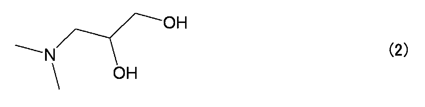
- a compound represented by the following formula (2) or a compound represented by the following formula (3) is particularly preferable.
- the copper complex preferably contains an inorganic anion and / or an organic anion as a ligand, and more preferably contains an organic anion as a ligand.
- organic anion include a conjugate base of carboxylic acid (carboxylate anion) and a conjugate base of acetylacetone or a derivative thereof (acetylacetonate anion or a derivative thereof).
- carboxylate anion examples include formic acid, acetic acid, trifluoroacetic acid, propionic acid, butyric acid, isobutyric acid, 2-methylbutyric acid, 2-ethylbutyric acid, valeric acid, isovaleric acid, pivalic acid, hexanoic acid, heptanoic acid, Examples thereof include conjugate bases such as octanoic acid, 2-ethylhexanoic acid, nonanoic acid, oxalic acid, malonic acid, benzoic acid, citric acid, and acetonedicarboxylic acid.
- acetylacetonate anion or a derivative thereof examples include acetylacetonate, 1,1,1-trimethylacetylacetonate, 1,1,1,5,5,5-hexamethylacetylacetonate, 1,1,1. -Trifluoroacetylacetonate, 1,1,1,5,5,5-hexafluoroacetylacetonate and the like.
- the formate anion or the acetate anion is preferable and the formate anion is more preferable because the conductivity of the conductive film to be obtained is more excellent.
- a copper complex containing a formate anion as a ligand is called a copper formate complex.
- the copper formate complex contains a formate anion and a compound represented by the formula (1) as a ligand.
- a particularly preferred copper formate complex includes two molecules of the formate anion and two molecules of the compound represented by the formula (1) in one molecule of the copper formate complex.
- the oxidation number of copper in the copper complex is not particularly limited, but from the viewpoint that the stability of the composition for forming a conductive film is better and the conductivity of the obtained conductive film is more excellent, + II or + I is Preferably, + II is more preferable.
- the method for synthesizing the copper complex is not particularly limited, and can be obtained, for example, by blending a copper carboxylate and a compound represented by the above formula (1). Alternatively, for example, it can be obtained by blending a complex of copper and acetylacetone or a derivative thereof with a compound represented by the above formula (1).
- the composition for forming a conductive film includes a thermoplastic polymer.
- a thermoplastic polymer can be used individually by 1 type or in combination of 2 or more types.
- thermoplastic polymer is not particularly limited, and examples thereof include cellulose resin, acrylic resin, polyester resin, polyether resin, polyolefin resin, polyurethane resin, polyamide resin, rosin compound, and vinyl polymer.
- examples of the cellulose resin include nitrocellulose, cellulose acetate, carboxymethylcellulose, and the like.
- acrylic resin examples include polymethyl acrylate (PAM) and polymethyl methacrylate (PMMA).
- polyester resin examples include polyethylene terephthalate (PET), polytrimethylene terephthalate (PTT), polybutylene terephthalate (PBT), polyethylene naphthalate (PEN), polybutylene naphthalate (PBN), and the like.
- polyether resin examples include polyacetal (POM), polyethylene oxide (PEO), polypropylene oxide (PPO), and modified polyphenylene ether (m-PPE).
- polyolefin resin examples include polyethylene (PE) and polypropylene (PP).
- polyamide resin examples include nylon 6, nylon 11, nylon 12, nylon 66, nylon 610, nylon 6T, nylon 6I, nylon 9T, nylon M5T, and the like.
- vinyl polymer examples include polyvinyl alcohol (PVA), polyvinyl pyrrolidone (PVP), polyvinyl acetate (PVAc), and the like.
- the thermoplastic polymer is preferably a hydrophilic polymer, more preferably at least one selected from the group consisting of polyvinyl pyrrolidone (PVP), polyvinyl alcohol (PVA) and polyethylene oxide (PEO), more preferably polyvinyl pyrrolidone or polyethylene oxide.
- PVP polyvinyl pyrrolidone
- PVA polyvinyl alcohol
- PEO polyethylene oxide
- Polyethylene oxide is more preferred.
- the reason why polyethylene oxide is preferable to polyvinyl pyrrolidone is that the harmfulness of a thermal decomposition product that is partially generated by heating during sintering is low.
- the weight average molecular weight of the thermoplastic polymer is not particularly limited, but is preferably 10,000 to 250,000, and more preferably 20,000 to 100,000, from the viewpoint of better conductivity and voids of the conductive film.
- the weight average molecular weight of the thermoplastic polymer is measured by GPC (gel permeation chromatography).
- the composition for forming a conductive film contains a solvent.
- a solvent copper oxide particles can be dispersed, and a copper complex as a copper precursor (hereinafter simply referred to as “copper complex”) and a thermoplastic polymer can be dissolved and does not react with them.
- copper complex a copper complex as a copper precursor (hereinafter simply referred to as “copper complex”) and a thermoplastic polymer can be dissolved and does not react with them.
- copper complex as a copper precursor
- thermoplastic polymer a thermoplastic polymer
- it is not particularly limited, for example, one selected from water, alcohols, ethers, esters, hydrocarbons, and aromatic hydrocarbons, or a mixture of two or more compatible types Is mentioned.
- water As the solvent, water, a water-soluble alcohol, an alkyl ether derived from the water-soluble alcohol, an alkyl ester derived from the water-soluble alcohol, or a mixture thereof is preferably used because of excellent compatibility with the copper complex.
- the water-soluble alcohol is preferably an aliphatic alcohol having a monovalent to trivalent hydroxy group, specifically, methanol, ethanol, 1-propanol, 1-butanol, 1-pentanol, 1-hexanol, cyclohexanol, 1-heptanol, 1-octanol, 1-nonanol, 1-decanol, glycidol, methylcyclohexanol, 2-methyl-1-butanol, 3-methyl-2-butanol, 4-methyl-2-pentanol, isopropyl alcohol, 2-ethylbutanol, 2-ethylhexanol, 2-octanol, terpineol, dihydroterpineol, 2-methoxyethanol, 2-ethoxyethanol, 2-n-butoxyethanol, carbitol, ethyl carbitol, n-butoxyethanol, carbitol, ethyl carbitol, n-
- aliphatic alcohols having 1 to 3 carbon atoms and having 1 to 3 valent hydroxy groups are preferable because they have a boiling point that is not too high and hardly remain after forming a conductive film.
- methanol, ethylene glycol, glycerol 2-methoxyethanol, diethylene glycol, and isopropyl alcohol are more preferable.
- ethers examples include alkyl ethers derived from the above alcohols, such as diethyl ether, diisobutyl ether, dibutyl ether, methyl-t-butyl ether, methyl cyclohexyl ether, diethylene glycol dimethyl ether, diethylene glycol diethyl ether, triethylene glycol dimethyl ether, triethylene glycol diethyl.
- alkyl ethers having 2 to 8 carbon atoms derived from aliphatic alcohols having 1 to 3 carbon atoms and having 1 to 3 valent hydroxy groups are preferred.
- diethyl ether, diethylene glycol dimethyl ether and tetrahydrofuran are more preferred.
- esters examples include alkyl esters derived from the above alcohols, such as methyl formate, ethyl formate, butyl formate, methyl acetate, ethyl acetate, butyl acetate, methyl propionate, ethyl propionate, butyl propionate, and ⁇ -butyrolactone. Illustrated. Of these, alkyl esters having 2 to 8 carbon atoms derived from aliphatic alcohols having 1 to 3 carbon atoms and having 1 to 3 valent hydroxy groups are preferred, and specifically methyl formate, ethyl formate, and methyl acetate are more preferred. .
- the main solvent is a solvent having the highest content in the solvent.
- composition for forming a conductive film may contain other components in addition to the copper oxide particles, the copper complex that is a copper precursor, the thermoplastic polymer, and the solvent.
- the composition for forming a conductive film may contain a rheology modifier (thixotropic agent, thixotropic agent).
- the rheology modifier imparts rheology to the conductive film-forming composition containing a solvent, and prevents dripping of the conductive film-forming composition applied or printed on the substrate before drying. This avoids contact between fine patterns.
- the rheology modifier is not particularly limited as long as it is a conventionally known rheology modifier used in a conductive film forming composition and does not adversely affect the conductivity and voids of the obtained conductive film. System rheology modifiers are preferred.
- organic rheology modifier examples include BYK-425 (a solution of urea-modified urethane urethane; manufactured by BYK Japan), BYK-428 (a solution of urethane having a large number of side chains; BYK Japan) Etc.).
- the conductive film forming composition may contain copper particles.
- a copper particle comprises the metallic copper in a electrically conductive film with the metallic copper which a copper oxide is reduce
- the copper particles are not particularly limited as long as they are conventionally known copper particles used in the conductive film-forming composition and do not adversely affect the flow characteristics of the conductive film-forming composition. Copper particles having a thickness of 0.1 to 2 ⁇ m are preferred.
- the average particle diameter of the copper particles is the volume median diameter (Dv50), and is measured using a particle diameter measuring machine such as FPAR-1000 (manufactured by Otsuka Electronics Co., Ltd., dynamic light scattering method). can do.
- the conductive film forming composition may contain a surfactant.
- the surfactant plays a role of improving the dispersibility of the copper oxide particles.
- the type of the surfactant is not particularly limited, and examples thereof include an anionic surfactant, a cationic surfactant, a nonionic surfactant, a fluorine surfactant, and an amphoteric surfactant. These surfactants can be used alone or in combination of two or more.
- the conductive film forming composition contains the above-described copper oxide particles, a copper complex that is a copper precursor, a thermoplastic polymer, and a solvent.
- content of the copper complex in the composition for electrically conductive film formation is not specifically limited, From the point that the electroconductivity of an electrically conductive film is more excellent, 5 mass% or more is preferable with respect to the total mass of a copper oxide particle. Further, from the viewpoint of less adverse effects on the conductivity and voids of the resulting conductive film, it is preferably 5 to 30% by mass, more preferably 10 to 30% by mass, and even more preferably 15 to 25% by mass.
- the content of the thermoplastic polymer in the composition for forming a conductive film is not particularly limited, but the total mass of the copper oxide particles is more excellent in the role as a primer for helping adhesion between the metallic copper and the base material. 3 mass% or more is preferable with respect to this. Further, from the viewpoint that the adverse effect on the conductivity of the obtained conductive film is less, it is more preferably 3 to 30% by mass, further preferably 3 to 15% by mass, and still more preferably 4 to 9% by mass.
- the content of the solvent in the composition for forming a conductive film is not particularly limited, but the increase in the viscosity of the composition for forming a conductive film is suppressed, and the handling property is superior, with respect to the total mass of the composition, 5 to 90% by mass is preferable, and 10 to 80% by mass is more preferable.
- the content of the copper particles in the conductive film-forming composition is not particularly limited, but from the viewpoint that the conductivity is further improved, 10 to 1500% by mass is preferable with respect to the mass.
- the content of the thixotropic agent in the conductive film-forming composition is not particularly limited, but the coating liquid before drying From the point that sagging is prevented and does not adversely affect the adhesion and conductivity of the conductive film to be formed, with respect to the total mass of the copper oxide particles (however, the composition for forming a conductive film contains copper particles) In this case, 0 to 5% by mass is preferable, and 0.5 to 3% by mass is more preferable.
- the content of the surfactant in the composition for forming a conductive film is not particularly limited, but from the viewpoint of improving the coating property, the total mass of the composition 0.0001 to 1% by mass is preferable, and 0.001 to 0.1% by mass is more preferable.
- the viscosity of the conductive film forming composition is preferably adjusted to a viscosity suitable for printing applications such as inkjet and screen printing.
- a viscosity suitable for printing applications such as inkjet and screen printing.
- inkjet discharge 1 to 50 cP is preferable, and 1 to 40 cP is more preferable.
- screen printing it is preferably from 1,000 to 100,000 cP, more preferably from 10,000 to 80,000 cP.
- the method for preparing the conductive film forming composition is not particularly limited, and a known method can be adopted.
- a known method can be adopted.
- known methods such as an ultrasonic method (for example, treatment with an ultrasonic homogenizer), a mixer method, a three-roll method, a ball mill method, etc.
- a composition can be obtained by dispersing the components by means.
- the method for producing a conductive film of the present invention comprises a step of forming a coating film on a substrate using the above-described composition for forming a conductive film (hereinafter also referred to as a coating film forming step as appropriate), heat treatment and / or light. And a step of obtaining a conductive film by performing irradiation treatment (hereinafter also referred to as a conductive film forming step). Below, each process is explained in full detail.
- This step is a step of forming a coating film by applying the above-described composition for forming a conductive film on a substrate.
- the precursor film before the reduction treatment is obtained in this step. You may dry a coating film before the electrically conductive film formation process mentioned later.
- the conductive film forming composition used is as described above.
- a well-known thing can be used as a base material used at this process.
- the material used for the substrate include resin, paper, glass, silicon-based semiconductor, compound semiconductor, metal oxide, metal nitride, wood, or a composite thereof. More specifically, low density polyethylene resin, high density polyethylene resin, ABS resin, acrylic resin, styrene resin, vinyl chloride resin, polyester resin (polyethylene terephthalate (PET)), polyacetal resin, polysulfone resin, polyetherimide resin Resin base materials such as polyetherketone resin, polyimide resin, cellulose derivative, etc .; non-coated printing paper, fine-coated printing paper, coated printing paper (art paper, coated paper), special printing paper, copy paper (PPC paper) ), Unbleached wrapping paper (both kraft paper for heavy bags, both kraft kraft paper), bleached wrapping paper (bleached kraft paper, pure white roll paper), coated balls, chipboard, corrugated cardboard and other paper substrates; soda glass, Glass substrates such as boro
- the method for applying the conductive film forming composition onto the substrate is not particularly limited, and a known method can be adopted.
- coating methods such as a screen printing method, a dip coating method, a spray coating method, a spin coating method, and an ink jet method can be used.
- the shape of application is not particularly limited, and may be a surface covering the entire surface of the substrate or a pattern (for example, a wiring or a dot).
- the coating amount of the composition for forming a conductive film on the substrate may be appropriately adjusted according to the desired film thickness of the conductive film.
- the film thickness of the coating film is preferably 0.1 to 100 ⁇ m, 0.1 to 50 ⁇ m is more preferable, 1 to 30 ⁇ m is more preferable, 1 to 20 ⁇ m is still more preferable, and 1 to 15 ⁇ m is even more preferable.
- This step is a step of performing a drying treatment on the formed coating film and removing the solvent. If desired, this step can be performed after the above-described coating film forming step and before the conductive film forming step described later. By removing the remaining solvent, in the conductive film forming step, generation of minute cracks and voids due to vaporization and expansion of the solvent can be suppressed, and the conductivity of the conductive film and the adhesion between the conductive film and the base material From the viewpoint of sex.
- a hot air dryer or the like can be used as a method for the drying treatment.
- the temperature is preferably 40 to 200 ° C., more preferably 50 to 150 ° C. More preferably, the heat treatment is performed at 70 ° C. to 120 ° C.
- an inert gas atmosphere such as nitrogen or argon is more preferable
- drying is preferably performed in a reducing gas atmosphere such as hydrogen.
- This step is a step of forming a conductive film containing metallic copper by performing heat treatment and / or light irradiation treatment on the formed coating film.
- the copper ions in the copper complex are reduced to metallic copper, the copper oxide in the copper oxide particles is reduced, and further sintered to obtain metallic copper.
- the metal copper generated from the copper complex and the copper oxide particles are Metal copper particles obtained by reduction are fused together to form grains, and the grains are further bonded and fused together to form a thin film.
- the light irradiation treatment it is presumed that the metal copper particles or the copper oxide particles absorb light and function as a photothermal conversion substance that converts the light into heat, and play a role of transferring heat into the coating film.
- the heating temperature is preferably 100 to 300 ° C., more preferably 150 to 250 ° C.
- the heating time is 5 to 120 minutes in that a conductive film having superior conductivity can be formed in a short time.
- 10 to 60 minutes are more preferable.
- the heating means is not particularly limited, and known heating means such as an oven and a hot plate can be used.
- the conductive film can be formed by heat treatment at a relatively low temperature, and therefore, the process cost is low.
- the light irradiation treatment can reduce and sinter to metallic copper by irradiating light on the portion to which the coating film is applied at room temperature for a short time, and heating for a long time.
- the base material does not deteriorate due to, and the adhesion of the conductive film to the base material becomes better.
- the light source used in the light irradiation treatment is not particularly limited, and examples thereof include a mercury lamp, a metal halide lamp, a xenon lamp, a chemical lamp, and a carbon arc lamp.
- Examples of radiation include electron beams, X-rays, ion beams, and far infrared rays.
- g-line, i-line, deep-UV light, and high-density energy beam (laser beam) are used.
- Specific examples of preferred embodiments include scanning exposure with an infrared laser, high-illuminance flash exposure such as a xenon discharge lamp, and infrared lamp exposure.
- the light irradiation is preferably light irradiation with a flash lamp, and more preferably pulsed light irradiation with a flash lamp. Irradiation with high-energy pulsed light can concentrate and heat the surface of the portion to which the coating film has been applied in a very short time, so that the influence of heat on the substrate can be extremely reduced.
- the irradiation energy of the pulse light is preferably 1 ⁇ 100J / cm 2, more preferably 1 ⁇ 30J / cm 2, preferably from 1 ⁇ sec ⁇ 100 m sec as a pulse width, and more preferably 10 ⁇ sec ⁇ 10 m sec.
- the irradiation time of the pulsed light is preferably 1 to 100 milliseconds, more preferably 1 to 50 milliseconds, and further preferably 1 to 20 milliseconds.
- the above heat treatment and light irradiation treatment may be performed alone or both may be performed simultaneously. Moreover, after performing one process, you may perform the other process further.
- the atmosphere in which the heat treatment and the light irradiation treatment are performed is not particularly limited, and examples include an air atmosphere, an inert atmosphere, or a reducing atmosphere.
- the inert atmosphere is, for example, an atmosphere filled with an inert gas such as argon, helium, neon, or nitrogen
- the reducing atmosphere is a reducing gas such as hydrogen or carbon monoxide. It refers to the atmosphere.
- a conductive film (metal copper film) containing metal copper is obtained.
- the film thickness of the conductive film is not particularly limited, and an optimum film thickness is appropriately adjusted according to the intended use. Of these, 0.01 to 1000 ⁇ m is preferable and 0.1 to 100 ⁇ m is more preferable from the viewpoint of printed wiring board use.
- the film thickness is a value (average value) obtained by measuring three or more thicknesses at arbitrary points on the conductive film and arithmetically averaging the values.
- the conductivity of the conductive film is evaluated by volume resistivity.
- the volume resistivity is less than 5 ⁇ 10 ⁇ 4 ⁇ ⁇ cm, preferably less than 1 ⁇ 10 ⁇ 4 ⁇ ⁇ cm, and more preferably less than 5 ⁇ 10 ⁇ 5 ⁇ ⁇ cm.
- the volume resistivity can be calculated by measuring the surface resistivity of the conductive film by the four-probe method and then multiplying the obtained surface resistivity by the film thickness.
- the void of the conductive film is evaluated by the void ratio.
- the void ratio is 30% or less, preferably 15% or less, and more preferably 5% or less. Note that the void ratio was obtained by arithmetically averaging the visual void ratio when the conductive film was processed with a focused ion beam (FIB) and the cross section was observed with a scanning electron microscope (SEM), and three points were randomly obtained. It can be calculated as a percentage.
- FIB focused ion beam
- SEM scanning electron microscope
- the conductive film may be provided on the entire surface of the base material or in a pattern.
- the patterned conductive film is useful as a conductor wiring (wiring) such as a printed wiring board.
- wiring conductor wiring
- the above-mentioned composition for forming a conductive film was applied to a substrate in a pattern, and the above heat treatment and / or light irradiation treatment was performed, or the entire surface of the substrate was provided.
- a method of etching the conductive film in a pattern may be used.
- the etching method is not particularly limited, and a known subtractive method, semi-additive method, or the like can be employed.
- an insulating layer (insulating resin layer, interlayer insulating film, solder resist) is further laminated on the surface of the patterned conductive film, and further wiring (metal) is formed on the surface. Pattern) may be formed.
- the material of the insulating film is not particularly limited.
- epoxy resin glass epoxy resin, aramid resin, crystalline polyolefin resin, amorphous polyolefin resin, fluorine-containing resin (polytetrafluoroethylene, perfluorinated polyimide, perfluorinated) Amorphous resin), polyimide resin, polyether sulfone resin, polyphenylene sulfide resin, polyether ether ketone resin, liquid crystal resin, and the like.
- an epoxy resin, a polyimide resin, or a liquid crystal resin and more preferably an epoxy resin. Specific examples include ABF GX-13 manufactured by Ajinomoto Fine Techno Co., Ltd.
- solder resist which is a kind of insulating layer material used for wiring protection, is described in detail in, for example, Japanese Patent Application Laid-Open No. 10-204150 and Japanese Patent Application Laid-Open No. 2003-222993. These materials can also be applied to the present invention if desired.
- solder resist commercially available products may be used. Specific examples include PFR800 manufactured by Taiyo Ink Manufacturing Co., Ltd., PSR4000 (trade name), SR7200G manufactured by Hitachi Chemical Co., Ltd., and the like.
- the base material (base material with a conductive film) having the conductive film obtained above can be used for various applications.
- a printed wiring board, TFT, FPC, RFID, etc. are mentioned.
- composition for forming conductive film Copper oxide particles; and (CI Kasei Co., NanoTek (R) CuO average particle diameter 50 nm) (70 mass parts), polyvinylpyrrolidone (PVP) and (weight-average molecular weight 220,000) (4 parts by mass), copper complex 1 (13 parts by mass), water (33 parts by mass), and a rheology modifier (BYK425, manufactured by Big Chemie Japan Co., Ltd.) (2 parts by mass) are mixed, and a revolving mixer (THINKY, manufactured by Aritori Kentaro ARE) -310) for 5 minutes to obtain a composition for forming a conductive film.
- a revolving mixer TINKY, manufactured by Aritori Kentaro ARE
- Example 2 (Synthesis of copper complex) Example 1 except that 2- (methylamino) ethanol (see formula below) (7.5 g; 100 mmol) was used instead of 3-dimethylamino-1,2-propanediol (11.9 g; 100 mmol) In the same manner as in Example 1, a copper formate complex was obtained. The obtained copper formate complex is hereinafter referred to as “copper complex 2”.
- a conductive film was prepared by preparing a composition for forming a conductive film in the same manner as in Example 1, except that the copper complex 2 (13 parts by mass) was used instead of the copper complex 1 (13 parts by mass).
- Example 3 (Synthesis of copper complex) Example 1 except that 2- (dimethylamino) ethanol (see formula below) (8.9 g; 100 mmol) was used instead of 3-dimethylamino-1,2-propanediol (11.9 g; 100 mmol)
- 2- (dimethylamino) ethanol see formula below
- 3-dimethylamino-1,2-propanediol 11.9 g; 100 mmol
- a conductive film was prepared by preparing a composition for forming a conductive film in the same manner as in Example 1 except that the copper complex 3 (13 parts by mass) was used instead of the copper complex 1 (13 parts by mass).
- Example 4 (Synthesis of copper complex) 1- (dimethylamino) -2-propanol (see formula below) (10.3 g; 100 mmol) was used in place of 3-dimethylamino-1,2-propanediol (11.9 g; 100 mmol).
- a copper formate complex was obtained.
- the obtained copper formate complex is hereinafter referred to as “copper complex 4”.
- a conductive film-forming composition was prepared in the same manner as in Example 1 except that copper complex 4 (13 parts by mass) was used instead of copper complex 1 (13 parts by mass) to produce a conductive film.
- Example 5 Synthesis of copper complex Similar to Example 1 except that 2-aminoethanol (see formula below) (6.1 g; 100 mmol) was used instead of 3-dimethylamino-1,2-propanediol (11.9 g; 100 mmol) Thus, a copper formate complex was obtained.
- the obtained copper formate complex is hereinafter referred to as “copper complex 5”.
- a conductive film-forming composition was prepared in the same manner as in Example 1 except that copper complex 5 (13 parts by mass) was used instead of copper complex 1 (13 parts by mass) to produce a conductive film.
- Example 6 (Synthesis of copper complex) Instead of 3-dimethylamino-1,2-propanediol (11.9 g; 100 mmol), 3- (diethylamino) -1,2-propanediol (see formula below) (14.7 g; 100 mmol) was used. Except for the points, a copper formate complex was obtained in the same manner as in Example 1. The obtained copper formate complex is hereinafter referred to as “copper complex 6”.
- a conductive film was prepared by preparing a composition for forming a conductive film in the same manner as in Example 1 except that the copper complex 6 (13 parts by mass) was used instead of the copper complex 1 (13 parts by mass).
- Example 7 (Synthesis of copper complex) Instead of 3-dimethylamino-1,2-propanediol (11.9 g; 100 mmol), 3- (methylamino) -1,2-propanediol (see formula below) (10.5 g; 100 mmol) was used. Except for the points, a copper formate complex was obtained in the same manner as in Example 1. The obtained copper formate complex is hereinafter referred to as “copper complex 7”.
- a conductive film-forming composition was prepared in the same manner as in Example 1 except that copper complex 7 (13 parts by mass) was used instead of copper complex 1 (13 parts by mass) to produce a conductive film.
- Example 8> Synthesis of copper complex Except that 3-amino-1,2-propanediol (see formula below) (9.1 g; 100 mmol) was used instead of 3-dimethylamino-1,2-propanediol (11.9 g; 100 mmol) In the same manner as in Example 1, a copper formate complex was obtained. The obtained copper formate complex is hereinafter referred to as “copper complex 8”.
- a conductive film was prepared by preparing a composition for forming a conductive film in the same manner as in Example 1, except that copper complex 8 (13 parts by mass) was used instead of copper complex 1 (13 parts by mass).
- Example 9 (Synthesis of copper complex) Example 2 except that 2,2′-iminodiethanol (see formula below) (10.5 g; 100 mmol) was used instead of 3-dimethylamino-1,2-propanediol (11.9 g; 100 mmol) In the same manner as in Example 1, a copper formate complex was obtained. The obtained copper formate complex is hereinafter referred to as “copper complex 9”.
- a conductive film was prepared by preparing a composition for forming a conductive film in the same manner as in Example 1 except that copper complex 9 (13 parts by mass) was used instead of copper complex 1 (13 parts by mass).
- Example 10 (Synthesis of copper complex) Except for using 2-amino-1,3-propanediol (see formula below) (9.1 g; 100 mmol) instead of 3-dimethylamino-1,2-propanediol (11.9 g; 100 mmol) In the same manner as in Example 1, a copper formate complex was obtained. The obtained copper formate complex is hereinafter referred to as “copper complex 10”.
- a conductive film-forming composition was prepared in the same manner as in Example 1 except that copper complex 10 (13 parts by mass) was used instead of copper complex 1 (13 parts by mass) to produce a conductive film.
- Example 11 (Synthesis of copper complex) Instead of 3-dimethylamino-1,2-propanediol (11.9 g; 100 mmol), 2-amino-2-hydroxymethyl-1,3-propanediol (see formula below) (12.1 g; 100 mmol) was used. Except for the points used, a copper formate complex was obtained in the same manner as in Example 1. The obtained copper formate complex is hereinafter referred to as “copper complex 11”.
- a conductive film forming composition was prepared in the same manner as in Example 1 except that the copper complex 11 (13 parts by mass) was used instead of the copper complex 1 (13 parts by mass) to produce a conductive film.
- Example 12 (Synthesis of copper complex) Instead of copper (II) formate tetrahydrate (manufactured by Kanto Chemical Co., Ltd.) (11.3 g; 50 mmol), copper (II) acetate (manufactured by Wako Pure Chemical Industries, Ltd.) (9.1 g; 50 mmol) was used. Except for the above, a copper acetate complex was obtained in the same manner as in Example 1. The obtained copper acetate complex is hereinafter referred to as “copper complex 12”.
- a conductive film was prepared by preparing a composition for forming a conductive film in the same manner as in Example 1, except that the copper complex 12 (13 parts by mass) was used instead of the copper complex 1 (13 parts by mass).
- Example 13> Synthesis of copper complex Except that acetylacetone copper (II) (manufactured by Kanto Chemical Co.) (13.1 g; 50 mmol) was used instead of copper (II) formate tetrahydrate (manufactured by Kanto Chemical Co., Ltd.) (11.3 g; 50 mmol) In the same manner as in Example 1, an acetylacetone copper complex was obtained. The obtained acetylacetone copper complex is hereinafter referred to as “copper complex 13”.
- a conductive film-forming composition was prepared in the same manner as in Example 1 except that the copper complex 13 (13 parts by mass) was used instead of the copper complex 1 (13 parts by mass) to produce a conductive film.
- Example 14 (Synthesis of copper complex) Instead of copper (II) formate tetrahydrate (Kanto Chemical Co., Ltd.) (11.3 g; 50 mmol), dicopper (I) oxalate 0.5 hydrate (Kanto Chemical Co., Ltd.) (11.2 g; A copper oxalate complex was obtained in the same manner as in Example 1 except that 50 mmol) was used. The obtained copper oxalate complex is hereinafter referred to as “copper complex 14”.
- a conductive film-forming composition was prepared in the same manner as in Example 1 except that copper complex 14 (13 parts by mass) was used instead of copper complex 1 (13 parts by mass) to produce a conductive film.
- Example 15 Preparation of conductive film forming composition / manufacture of conductive film
- copper oxide particles Ci Kasei Co., Ltd., NanoTek (R) CuO; average particle size 50 nm
- copper oxide particles comprising copper oxide (I) manufactured by Hefei; average particle size 20 nm
- a conductive film-forming composition was prepared in the same manner as in Example 1 to produce a conductive film.
- Example 16> Preparation of conductive film forming composition / manufacture of conductive film
- PVA polyvinyl alcohol
- a conductive film-forming composition was prepared in the same manner as in Example 1 to produce a conductive film.
- Example 17 (Preparation of conductive film forming composition / manufacture of conductive film) Implemented except that polyethylene pyrrolidone (mass average molecular weight 220,000) (4 parts by mass) was replaced by polyethylene oxide (PEO) (Sigma Aldrich, mass average molecular weight 200,000) (4 parts by mass).
- PEO polyethylene oxide
- a conductive film-forming composition was prepared in the same manner as in Example 1 to produce a conductive film.
- Example 18 Preparation of conductive film forming composition / manufacture of conductive film
- polyvinyl pyrrolidone mass average molecular weight 220,000
- PA polyacrylic acid
- a conductive film forming composition was prepared in the same manner as in Example 1 to produce a conductive film.
- Example 19 (Preparation of conductive film forming composition / manufacture of conductive film) Except for using polyacrylamide (PAM) (manufactured by Sigma-Aldrich, mass average molecular weight 10,000) (4 parts by mass) instead of polyvinylpyrrolidone (mass average molecular weight 220,000) (4 parts by mass) A conductive film-forming composition was prepared in the same manner as in Example 1 to produce a conductive film.
- PAM polyacrylamide
- a conductive film-forming composition was prepared in the same manner as in Example 1 to produce a conductive film.
- ⁇ Comparative example 1> (Preparation of conductive film forming composition / manufacture of conductive film) A conductive film forming composition was prepared in the same manner as in Example 1, except that copper formate tetrahydrate (13 parts by mass) was used instead of copper complex 1 (13 parts by mass). A conductive film was produced.
- a conductive film-forming composition was prepared in the same manner as in Example 1 except that copper complex C2 (13 parts by mass) was used instead of copper complex 1 (13 parts by mass) to produce a conductive film.
- a conductive film-forming composition was prepared in the same manner as in Example 1 except that copper complex C3 (13 parts by mass) was used instead of copper complex 1 (13 parts by mass) to produce a conductive film.
- a conductive film was prepared by preparing a composition for forming a conductive film in the same manner as in Example 1 except that the copper complex C4 (13 parts by mass) was used instead of the copper complex 1 (13 parts by mass).
- Example 1 was repeated except that ethylene glycol (see formula below) (6.2 g; 100 mmol) was used instead of 3-dimethylamino-1,2-propanediol (11.9 g; 100 mmol). A copper formate complex was obtained. The obtained copper formate complex is hereinafter referred to as “copper complex C5”.
- a conductive film was prepared by preparing a composition for forming a conductive film in the same manner as in Example 1, except that the copper complex C5 (13 parts by mass) was used instead of the copper complex 1 (13 parts by mass).
- Example 6 A conductive film-forming composition was prepared in the same manner as in Example 1 except that copper oxide particles (manufactured by CI Kasei Co., Ltd., NanoTek (R) CuO; average particle diameter 50 nm) were not used. Manufactured.
- Example 8 A conductive film-forming composition was prepared in the same manner as in Example 1 except that polyvinylpyrrolidone (mass average molecular weight 220,000) (4 parts by mass) was not used, and a conductive film was produced.
- polyvinylpyrrolidone mass average molecular weight 220,000
- Table 1 shows the compositions of the conductive film forming compositions of Examples 1 to 19 and Comparative Examples 1 to 8.
- void> The voids of the conductive films of Examples 1 to 19 and Comparative Examples 1 to 8 were evaluated by the following methods.
- a to C are desirable for practical use.
- B ... Void ratio 6-15%
- C ... Void rate 16-30%
- D ... Void rate 31 ⁇ 50% E ... Void ratio 51% or more
- Table 1 shows the evaluation results of conductivity and voids.
- Examples 1 to 19 are compared with Comparative Examples 1 to 8, the conductivity and voids of the conductive films of Examples 1 to 19 containing a copper complex containing the compound of the above formula (1) as a ligand are excellent. It was. Further, when Examples 1 and 6 to 11 are compared with Examples 2 to 5, it contains a copper complex containing a compound represented by the formula (1) having two or more hydroxy groups as a ligand. Examples 1 and 6 to 11 are obtained as compared with Examples 2 to 5 containing a copper complex having one hydroxy group and containing a compound represented by the formula (1) as a ligand. The conductivity of the conductive film was excellent.
- Example 1 containing a copper complex containing a compound represented by the formula (1), which is a tertiary amine, as a ligand 6 is a primary or secondary amine, compared to Examples 7 to 11 containing a copper complex containing a compound represented by the formula (1) as a ligand.
- the void was excellent.
- Examples 1, 12, and 13 are compared with Example 14, Examples 1, 12, and 14 containing a copper complex having a copper oxidation number of + II in the copper complex have a copper oxidation number of + I. Compared with Example 14 containing a certain copper complex, the electroconductivity of the electrically conductive film obtained was excellent.
- Example 1 when Example 1 is compared with Examples 12 and 13, the conductive film obtained in Example 1 containing the copper formate complex was obtained compared to Examples 12 and 13 containing the copper acetate complex or acetylacetone copper complex. The conductivity and void were excellent.
- Example 1 When Example 1 is compared with Example 15, Example 1 containing copper oxide particles made of copper (II) oxide is more in comparison with Example 15 containing copper oxide particles made of copper (I) oxide. The conductivity and voids of the obtained conductive film were excellent. Comparing Examples 1, 16 and 17 with Examples 18 and 19, Examples 1, 16 and 17 containing PVP, PVA or PEO as the thermoplastic polymer are Examples 18 and 19 containing PA or PAM. Compared with, conductivity and voids were excellent. Further, when Examples 1 and 17 and Example 16 are compared, Example 17 containing PVP or PEO as a thermoplastic polymer is more excellent in conductivity or void than Example 16 containing PVA. It was.
Landscapes
- Chemical & Material Sciences (AREA)
- Engineering & Computer Science (AREA)
- Life Sciences & Earth Sciences (AREA)
- Materials Engineering (AREA)
- Wood Science & Technology (AREA)
- Organic Chemistry (AREA)
- Inorganic Chemistry (AREA)
- Dispersion Chemistry (AREA)
- Chemical Kinetics & Catalysis (AREA)
- Microelectronics & Electronic Packaging (AREA)
- Conductive Materials (AREA)
- Paints Or Removers (AREA)
- Manufacturing Of Printed Wiring (AREA)
- Manufacturing Of Electric Cables (AREA)
- Parts Printed On Printed Circuit Boards (AREA)
- Compositions Of Macromolecular Compounds (AREA)
Abstract
酸化銅粒子(A)と、銅前駆体である銅錯体(B)と、熱可塑性ポリマー(C)と、溶媒(D)とを含有し、銅錯体(B)に含まれる配位子が一般式(1)で表される化合物を含む、導電性に優れ、かつ、ボイドの少ない導電膜を形成することができる導電膜形成用組成物が提供される。
Description
本発明は、導電膜形成用組成物に係り、特に、酸化銅粒子と、所定の銅錯体と、熱可塑性ポリマーと、溶媒とを含有する導電膜形成用組成物に関する。
また、本発明は、導電膜の製造方法に係り、特に、上記導電膜形成用組成物を用いた導電膜の製造方法に関する。
また、本発明は、導電膜の製造方法に係り、特に、上記導電膜形成用組成物を用いた導電膜の製造方法に関する。
基材上に金属膜を形成する方法として、金属粒子または金属酸化物粒子の分散体を印刷法により基材に塗布し、加熱処理または光照射処理して焼結させることによって金属膜や回路基板における配線等の電気的導通部位を形成する技術が知られている。
上記方法は、従来の高熱・真空プロセス(スパッタ)やめっき処理による配線作製法に比べて、簡便・省エネ・省資源であることから次世代エレクトロニクス開発において大きな期待を集めている。
上記方法は、従来の高熱・真空プロセス(スパッタ)やめっき処理による配線作製法に比べて、簡便・省エネ・省資源であることから次世代エレクトロニクス開発において大きな期待を集めている。
より具体的には、特許文献1においては、銅微粒子、銅前駆体、および還元剤を含有する導電膜形成用組成物を用いて塗膜を形成し、さらに焼成することにより導電膜を形成する方法が開示されている。
また、特許文献2においては、特定構造のアミン化合物およびギ酸銅を含む銅前駆体組成物を基板上に塗布し、加熱処理することによる銅膜の製造方法が開示されている。
また、特許文献3においては、還元力を有するカルボン酸と銅イオンとからなる銅塩の微粒子(A)および配位性化合物(B)を含有する導電性インク組成物を、基材中の電気的導通を得たいと所望する部位に塗布または充填し、当該基材を加熱処理することを特徴とする電気的導通部位の製造方法が開示されている。
また、特許文献2においては、特定構造のアミン化合物およびギ酸銅を含む銅前駆体組成物を基板上に塗布し、加熱処理することによる銅膜の製造方法が開示されている。
また、特許文献3においては、還元力を有するカルボン酸と銅イオンとからなる銅塩の微粒子(A)および配位性化合物(B)を含有する導電性インク組成物を、基材中の電気的導通を得たいと所望する部位に塗布または充填し、当該基材を加熱処理することを特徴とする電気的導通部位の製造方法が開示されている。
一方、近年、低コスト化の観点から、酸化銅粒子を含む組成物を用いて金属銅を含有する導電膜を形成する方法の開発が要望されている。
本発明者らが、特許文献1~3に記載の導電膜形成用組成物を用いて得られる導電膜の導電性およびボイドを検討したところ、導電性およびボイドのいずれも所望の性能を示さず、さらなる改良が必要であった。
本発明者らが、特許文献1~3に記載の導電膜形成用組成物を用いて得られる導電膜の導電性およびボイドを検討したところ、導電性およびボイドのいずれも所望の性能を示さず、さらなる改良が必要であった。
本発明は、上記実情に鑑みて、導電性に優れ、かつ、ボイドの少ない導電膜を形成することができる導電膜形成用組成物を提供することを目的とする。
本発明者らは、従来技術の問題点について鋭意検討した結果、酸化銅粒子と、所定の銅錯体と、熱可塑性ポリマーと、溶媒とを使用することにより、上記課題を解決できることを見出した。
すなわち、以下の構成により上記目的を達成することができることを見出した。
すなわち、以下の構成により上記目的を達成することができることを見出した。
(1)酸化銅粒子(A)と、銅前駆体である銅錯体(B)と、熱可塑性ポリマー(C)と、溶媒(D)とを含有し、銅錯体(B)に含まれる配位子が一般式(1)で表される化合物を含む導電膜形成用組成物。

[式中、R1、R2、R3、R4、R5およびR6は、それぞれ独立に、水素原子、アルキル基、アルコキシ基、アリール基、ヘテロアリール基、アミノ基、アルキルアミノ基、ヒドロキシ基およびヒドロキシアルキル基からなる群から選択される置換基であり、R1、R2、R3、R4、R5およびR6から選択される2以上の置換基は互いに結合して環構造を形成してもよい。]
(2)銅錯体(B)において、式(1)中、R6が水素原子であり、かつ、R1~R5のうち少なくとも1つがヒドロキシ基またはヒドロキシアルキル基である、(1)に記載の導電膜形成用組成物。
(3)銅錯体(B)において、式(1)中、R1およびR2のうち少なくとも1つがアルキル基である、(2)に記載の導電膜形成用組成物。
(4)銅錯体(B)において、銅の酸化数が+IIである、(1)~(3)のいずれか1項に記載の導電膜形成用組成物。
(5)銅錯体(B)がギ酸銅錯体である、(1)~(4)のいずれか1項に記載の導電膜形成用組成物。
(6)熱可塑性ポリマー(C)が親水性ポリマーである、(1)~(5)のいずれか1項に記載の導電膜形成用組成物。
(7)酸化銅粒子(A)が酸化銅(II)からなる、(1)~(6)のいずれか1項に記載の導電膜形成用組成物。
(8)熱可塑性ポリマー(C)がポリビニルピロリドン、ポリビニルアルコールおよびポリエチレンオキシドからなる群から選択される少なくとも1つである、(1)~(7)のいずれか1項に記載の導電膜形成用組成物。
(9)(1)~(8)のいずれか1項に記載の導電膜形成用組成物を基材上に付与して、塗膜を形成する塗膜形成工程と、塗膜に対して加熱および/または光照射による焼結処理を行い、導電膜を形成する導電膜形成工程とを備える、導電膜の製造方法。
(10)焼結処理がレーザー光照射またはパルス光照射により行われる、(9)に記載の導電膜の製造方法。
(2)銅錯体(B)において、式(1)中、R6が水素原子であり、かつ、R1~R5のうち少なくとも1つがヒドロキシ基またはヒドロキシアルキル基である、(1)に記載の導電膜形成用組成物。
(3)銅錯体(B)において、式(1)中、R1およびR2のうち少なくとも1つがアルキル基である、(2)に記載の導電膜形成用組成物。
(4)銅錯体(B)において、銅の酸化数が+IIである、(1)~(3)のいずれか1項に記載の導電膜形成用組成物。
(5)銅錯体(B)がギ酸銅錯体である、(1)~(4)のいずれか1項に記載の導電膜形成用組成物。
(6)熱可塑性ポリマー(C)が親水性ポリマーである、(1)~(5)のいずれか1項に記載の導電膜形成用組成物。
(7)酸化銅粒子(A)が酸化銅(II)からなる、(1)~(6)のいずれか1項に記載の導電膜形成用組成物。
(8)熱可塑性ポリマー(C)がポリビニルピロリドン、ポリビニルアルコールおよびポリエチレンオキシドからなる群から選択される少なくとも1つである、(1)~(7)のいずれか1項に記載の導電膜形成用組成物。
(9)(1)~(8)のいずれか1項に記載の導電膜形成用組成物を基材上に付与して、塗膜を形成する塗膜形成工程と、塗膜に対して加熱および/または光照射による焼結処理を行い、導電膜を形成する導電膜形成工程とを備える、導電膜の製造方法。
(10)焼結処理がレーザー光照射またはパルス光照射により行われる、(9)に記載の導電膜の製造方法。
本発明によれば、導電性に優れ、かつ、ボイドの少ない導電膜を形成することができる導電膜形成用組成物を提供することができる。
また、本発明によれば、該導電膜形成用組成物を用いた導電膜の製造方法を提供することもできる。
また、本発明によれば、該導電膜形成用組成物を用いた導電膜の製造方法を提供することもできる。
以下に、本発明の導電膜形成用組成物および導電膜の製造方法の好適態様について詳述する。
まず、本発明の従来技術と比較した特徴点について詳述する。
まず、本発明の従来技術と比較した特徴点について詳述する。
〈酸化銅粒子〉
導電膜形成用組成物には、酸化銅粒子が含まれる。酸化銅粒子は、後述する加熱処理または光照射処理によって酸化銅が金属銅に還元され、導電膜中の金属銅を構成する。なお、後述するように、導電膜形成用組成物に銅粒子が含まれる場合は、酸化銅粒子の酸化銅が還元されて生成する金属銅粒子とともに、導電膜中の金属銅を構成する。
導電膜形成用組成物には、酸化銅粒子が含まれる。酸化銅粒子は、後述する加熱処理または光照射処理によって酸化銅が金属銅に還元され、導電膜中の金属銅を構成する。なお、後述するように、導電膜形成用組成物に銅粒子が含まれる場合は、酸化銅粒子の酸化銅が還元されて生成する金属銅粒子とともに、導電膜中の金属銅を構成する。
本発明における「酸化銅」とは、酸化されていない銅を実質的に含まない化合物であり、具体的には、X線回折による結晶解析において、酸化銅由来のピークが検出され、かつ金属銅由来のピークが検出されない化合物のことを指す。銅を実質的に含まないとは、限定的ではないが、銅の含有量が酸化銅粒子に対して1質量%以下であることをいう。
酸化銅としては、酸化銅(I)または酸化銅(II)が好ましく、安価に入手可能であること、低抵抗であることから酸化銅(II)であることがさらに好ましい。すなわち、酸化銅粒子としては、酸化銅(II)からなる酸化銅粒子または酸化銅(I)からなる酸化銅粒子が好ましく、酸化銅(II)からなる酸化銅粒子がより好ましい。
酸化銅粒子の平均粒子径は、特に限定されないが、50~500nmが好ましく、70~250nmがより好ましく、80~180nmがさらに好ましい。この範囲内であると、本発明の導電膜形成用組成物を用いて得られる導電膜の導電性およびボイドがより優れたものとなる。なお、本発明において、酸化銅粒子の平均粒子径は体積中位径(Dv50)であり、例えば、FPAR-1000(大塚電子社製、動的光散乱方式)等の粒子径測定機を用いて測定することができる。
酸化銅粒子としては、粉末または分散液のどちらでも利用することができ、導電膜形成用組成物に用いられる公知の酸化銅粒子であって、平均粒子径が上記範囲内のものであれば、特に制限されない。具体的には、酸化銅(II)粒子としては、NanoTek CuO(シーアイ化成社製)、酸化銅(II)ナノ粒子(シグマアルドリッチ社製)、酸化銅(II)ナノ粒子(イオリテック社製)等が挙げられ。酸化銅(I)粒子としては、酸化銅(I)粒子(Hefei社製)等が挙げられる。
〈銅前駆体である銅錯体〉
導電膜形成用組成物には、銅前駆体である銅錯体(本項目において、以下、単に「銅錯体」という。)が含まれる。銅錯体は、後述する後述する加熱処理または光照射処理によって、銅錯体中の銅(+II)または銅(+I)が還元されて銅(0)が生成し、生成した銅(0)が導電性接着剤として働き、酸化銅粒子の酸化銅が還元されて生成する金属銅粒子間の融着を促進する効果がある。なお、後述するように、導電膜形成用組成物が含まれる場合は、酸化銅粒子の酸化銅が還元されて生成する金属銅粒子間、酸化銅粒子の酸化銅が還元されて生成する金属銅粒子と銅粒子間および銅粒子間の融着を促進する効果がある。
導電膜形成用組成物には、銅前駆体である銅錯体(本項目において、以下、単に「銅錯体」という。)が含まれる。銅錯体は、後述する後述する加熱処理または光照射処理によって、銅錯体中の銅(+II)または銅(+I)が還元されて銅(0)が生成し、生成した銅(0)が導電性接着剤として働き、酸化銅粒子の酸化銅が還元されて生成する金属銅粒子間の融着を促進する効果がある。なお、後述するように、導電膜形成用組成物が含まれる場合は、酸化銅粒子の酸化銅が還元されて生成する金属銅粒子間、酸化銅粒子の酸化銅が還元されて生成する金属銅粒子と銅粒子間および銅粒子間の融着を促進する効果がある。
銅錯体は、それに含まれる配位子が一般式(1)で表される化合物を含むものであれば、特に限定されない。
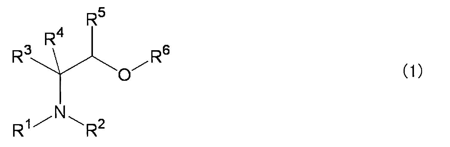
[式中、R1、R2、R3、R4、R5およびR6は、それぞれ独立に、水素原子、アルキル基、アルコキシ基、アリール基、ヘテロアリール基、アミノ基、アルキルアミノ基、ヒドロキシ基およびヒドロキシアルキル基からなる群から選択される置換基であり、R1、R2、R3、R4、R5およびR6から選択される2つ以上の置換基は互いに結合して環構造を形成してもよい。]
上記化合物としては、具体的には、例えば、以下に掲げるものが挙げられる。
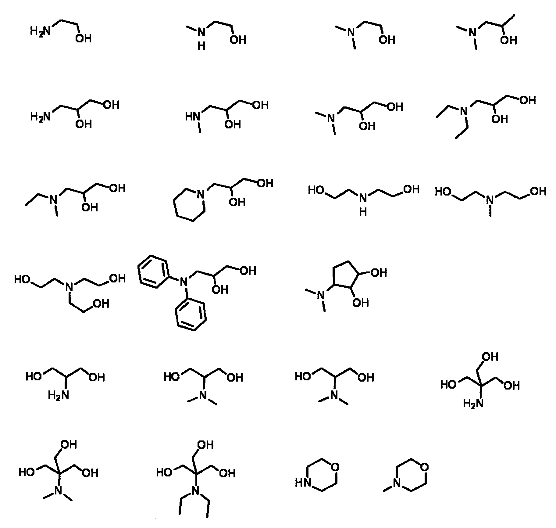
上記化合物としては、式(1)中、R6が水素原子であり、かつ、R1~R5のうち少なくとも1つがヒドロキシ基またはヒドロキシアルキル基であるものが好ましい。R1~R5のいずれか1つ以上の置換基がヒドロキシ基またはヒドロキシアルキル基であってもよいが、R3~R5のいずれか1つ以上の置換基がヒドロキシ基またはヒドロキシアルキル基であることが好ましい。化合物が1分子中に2つ以上のヒドロキシ基を有すると、導電性がより優れたものとなる。
さらに、上記化合物としては、式(1)中、R1およびR2のうち少なくとも1つがアルキル基であるものがより好ましい。式(1)で表される化合物は第二級アミンまたは第三級アミンであることが好ましく、第三級アミンであることがより好ましい。第二級アミンまたは第三級アミンであるとボイドがより低くなり、第三級アミンであると導電性がさらに良好なものとなる。
式(1)で表される化合物としては、とりわけ、下記式(2)で表されるもの、または下記式(3)で表されるものが好ましい。

銅錯体は上記一般式(1)で表される化合物以外に、無機アニオンおよび/または有機アニオンを配位子として含むことが好ましく、有機アニオンを配位子として含むことがより好ましい。有機アニオンとしては、カルボン酸の共役塩基(カルボキシラートアニオン)、およびアセチルアセトンまたはその誘導体の共役塩基(アセチルアセトナートアニオンまたはその誘導体)が好適な例として挙げられる。
カルボキシラートアニオンとしては、例えば、ギ酸、酢酸、トリフルオロ酢酸、プロピオン酸、酪酸、イソ酪酸、2-メチル酪酸、2-エチル酪酸、吉草酸、イソ吉草酸、ピバリン酸、ヘキサン酸、ヘプタン酸、オクタン酸、2-エチルヘキサン酸、ノナン酸、シュウ酸、マロン酸、安息香酸、クエン酸、アセトンジカルボン酸等の共役塩基が挙げられる。
アセチルアセトナートアニオンまたはその誘導体としては、例えば、アセチルアセトナート、1,1,1-トリメチルアセチルアセトナート、1,1,1,5,5,5-ヘキサメチルアセチルアセトナート、1,1,1-トリフルオロアセチルアセトナート、1,1,1,5,5,5-ヘキサフルオロアセチルアセトナート等が挙げられる。
これらの中でも、コストおよび得られる導電膜の導電性がより優れたものになることから、ギ酸アニオンまたは酢酸アニオンが好ましく、ギ酸アニオンがより好ましい。ギ酸アニオンを配位子として含む銅錯体をギ酸銅錯体という。特に、本発明においては、ギ酸銅錯体は、配位子として、ギ酸アニオンと、式(1)で表される化合物とを含む。特に好ましいギ酸銅錯体は、ギ酸銅錯体1分子中に、ギ酸アニオン2分子と、式(1)で表される化合物2分子とを含むものである。
また、銅錯体中の銅の酸化数は、特に限定されないが、導電膜形成用組成物の安定性がより良好であり、得られる導電膜の導電性がより優れるという点から、+IIまたは+Iが好ましく、+IIがより好ましい。
銅錯体の合成方法は、特に限定されるものではないが、例えば、銅カルボン酸塩と、上記式(1)で表される化合物とを配合することによって得られる。あるいは、例えば、銅とアセチルアセトンもしくはその誘導体との錯体と、上記式(1)で表される化合物とを配合することによって得られる。
〈熱可塑性ポリマー〉
導電膜形成用組成物には、熱可塑性ポリマーが含まれる。また、熱可塑性ポリマーは、1種類を単独で、または2種類以上を組み合わせて使用することができる。
導電膜形成用組成物には、熱可塑性ポリマーが含まれる。また、熱可塑性ポリマーは、1種類を単独で、または2種類以上を組み合わせて使用することができる。
熱可塑性ポリマーの種類は特に限定されないが、例えば、セルロース樹脂、アクリル樹脂、ポリエステル樹脂、ポリエーテル樹脂、ポリオレフィン樹脂、ポリウレタン樹脂、ポリアミド樹脂、ロジン配合物およびビニル系ポリマーが挙げられる。セルロース系樹脂としては、例えば、ニトロセルロース、酢酸セルロース、カルボキシメチルセルロース等が挙げられる。
アクリル樹脂としては、例えば、ポリアクリル酸メチル(PAM)、ポリメタクリル酸メチル(PMMA)等が挙げられる。ポリエステル樹脂としては、例えば、ポリエチレンテレフタラート(PET)、ポリトリメチレンテレフタラート(PTT)、ポリブチレンテレフタラート(PBT)、ポリエチレンナフタラート(PEN)、ポリブチレンナフタラート(PBN)等が挙げられる。ポリエーテル樹脂としては、例えば、ポリアセタール(POM)、ポリエチレンオキシド(PEO)、ポリプロピレンオキシド(PPO)、変性ポリフェニレンエーテル(m-PPE)等が挙げられる。ポリオレフィン樹脂としては、例えば、ポリエチレン(PE)、ポリプロピレン(PP)等が挙げられる。ポリアミド樹脂としては、例えば、ナイロン6、ナイロン11、ナイロン12、ナイロン66、ナイロン610、ナイロン6T、ナイロン6I、ナイロン9T、ナイロンM5T等が挙げられる。ビニル系ポリマーとしては、例えば、ポリビニルアルコール(PVA)、ポリビニルピロリドン(PVP)、ポリ酢酸ビニル(PVAc)等が挙げられる。
熱可塑性ポリマーとしては親水性ポリマーが好ましく、ポリビニルピロリドン(PVP)、ポリビニルアルコール(PVA)およびポリエチレンオキシド(PEO)からなる群から選択される少なくとも1種がより好ましく、ポリビニルピロリドンまたはポリエチレンオキシドがさらに好ましく、ポリエチレンオキシドがいっそう好ましい。ポリエチレンオキシドがポリビニルピロリドンよりも好ましい理由としては、焼結時の加熱によって一部発生する熱分解生成物の有害性が低い点が挙げられる。
熱可塑性ポリマーの重量平均分子量は、特に限定されないが、導電膜の導電性およびボイドがより優れる点で、10,000~250,000が好ましく、20,000~100,000がより好ましい。なお、熱可塑性ポリマーの重量平均分子量はGPC(ゲル浸透クロマトグラフィー)にて測定する。
〈溶媒〉
導電膜形成用組成物には、溶媒が含まれる。溶媒としては、酸化銅粒子を分散させ、かつ、銅前駆体である銅錯体(本項目において、以下、単に「銅錯体」という。)および熱可塑性ポリマーを溶解させることができ、それらと反応しないものであれば、特に限定するものではないが、例えば、水、アルコール類、エーテル類、エステル類、炭化水素類および芳香族炭化水素類から選ばれる一種、または相溶性のある二種以上の混合物が挙げられる。
導電膜形成用組成物には、溶媒が含まれる。溶媒としては、酸化銅粒子を分散させ、かつ、銅前駆体である銅錯体(本項目において、以下、単に「銅錯体」という。)および熱可塑性ポリマーを溶解させることができ、それらと反応しないものであれば、特に限定するものではないが、例えば、水、アルコール類、エーテル類、エステル類、炭化水素類および芳香族炭化水素類から選ばれる一種、または相溶性のある二種以上の混合物が挙げられる。
溶媒としては、銅錯体との相溶性に優れることから、水、水溶性アルコール、この水溶性アルコール由来のアルキルエーテル、この水溶性アルコール由来のアルキルエステル、またはこれらの混合物が好ましく用いられる。
水としては、イオン交換水のレベルの純度を有するものが好ましい。
水溶性アルコールとしては、1~3価のヒドロキシ基を有する脂肪族アルコールが好ましく、具体的には、メタノール、エタノール、1-プロパノール、1-ブタノール、1-ペンタノール、1-ヘキサノール、シクロヘキサノール、1-ヘプタノール、1-オクタノール、1-ノナノール、1-デカノール、グリシドール、メチルシクロヘキサノール、2-メチル-1-ブタノール、3-メチル-2-ブタノール、4-メチル-2-ペンタノール、イソプロピルアルコール、2-エチルブタノール、2-エチルヘキサノール、2-オクタノール、テルピネオール、ジヒドロテルピネオール、2-メトキシエタノール、2-エトキシエタノール、2-n-ブトキシエタノール、カルビトール、エチルカルビトール、n-ブチルカルビトール、ジアセトンアルコール、エチレングリコール、ジエチレングリコール、トリエチレングリコール、テトラエチレングリコール、プロピレングリコール、トリメチレングリコール、ジプロピレングリコール、トリプロピレングリコール、1,2-ブチレングリコール、1,3-ブチレングリコール、1,4-ブチレングリコール、ペンタメチレングリコール、へキシレングリコール、グリセリン等が挙げられる。
なかでも、1~3価のヒドロキシ基を有する炭素数1~6の脂肪族アルコールは、沸点が高すぎず導電膜形成後に残存しにくいことから好ましく、具体的には、メタノール、エチレングリコール、グリセリン、2-メトキシエタノール、ジエチレングリコール、イソプロピルアルコールがより好ましい。
水溶性アルコールとしては、1~3価のヒドロキシ基を有する脂肪族アルコールが好ましく、具体的には、メタノール、エタノール、1-プロパノール、1-ブタノール、1-ペンタノール、1-ヘキサノール、シクロヘキサノール、1-ヘプタノール、1-オクタノール、1-ノナノール、1-デカノール、グリシドール、メチルシクロヘキサノール、2-メチル-1-ブタノール、3-メチル-2-ブタノール、4-メチル-2-ペンタノール、イソプロピルアルコール、2-エチルブタノール、2-エチルヘキサノール、2-オクタノール、テルピネオール、ジヒドロテルピネオール、2-メトキシエタノール、2-エトキシエタノール、2-n-ブトキシエタノール、カルビトール、エチルカルビトール、n-ブチルカルビトール、ジアセトンアルコール、エチレングリコール、ジエチレングリコール、トリエチレングリコール、テトラエチレングリコール、プロピレングリコール、トリメチレングリコール、ジプロピレングリコール、トリプロピレングリコール、1,2-ブチレングリコール、1,3-ブチレングリコール、1,4-ブチレングリコール、ペンタメチレングリコール、へキシレングリコール、グリセリン等が挙げられる。
なかでも、1~3価のヒドロキシ基を有する炭素数1~6の脂肪族アルコールは、沸点が高すぎず導電膜形成後に残存しにくいことから好ましく、具体的には、メタノール、エチレングリコール、グリセリン、2-メトキシエタノール、ジエチレングリコール、イソプロピルアルコールがより好ましい。
エーテル類としては、上記アルコール由来のアルキルエーテルが挙げられ、ジエチルエーテル、ジイソブチルエーテル、ジブチルエーテル、メチル-t-ブチルエーテル、メチルシクロヘキシルエーテル、ジエチレングリコールジメチルエーテル、ジエチレングリコールジエチルエーテル、トリエチレングリコールジメチルエーテル、トリエチレングリコールジエチルエーテル、テトラヒドロフラン、テトラヒドロピラン、1,4-ジオキサン等が例示される。なかでも、1~3価のヒドロキシ基を有する炭素数1~4の脂肪族アルコール由来の炭素数2~8のアルキルエーテルが好ましく、具体的には、ジエチルエーテル、ジエチレングリコールジメチルエーテル、テトラヒドロフランがより好ましい。
エステル類としては、上記アルコール由来のアルキルエステルが挙げられ、ギ酸メチル、ギ酸エチル、ギ酸ブチル、酢酸メチル、酢酸エチル、酢酸ブチル、プロピオン酸メチル、プロピオン酸エチル、プロピオン酸ブチル、γ-ブチロラクトン等が例示される。なかでも、1~3価のヒドロキシ基を有する炭素数1~4の脂肪族アルコール由来の炭素数2~8のアルキルエステルが好ましく、具体的には、ギ酸メチル、ギ酸エチル、酢酸メチルがより好ましい。
上記溶媒の中でも、沸点が高すぎないことから、特に水または水溶性アルコールを主溶媒として用いることが好ましい。主溶媒とは、溶媒の中で含有率が最も多い溶媒である。
〈その他成分〉
導電膜形成用組成物には、上記酸化銅粒子、銅前駆体である銅錯体、熱可塑性ポリマーおよび溶媒以外にも他の成分が含まれていてもよい。
導電膜形成用組成物には、上記酸化銅粒子、銅前駆体である銅錯体、熱可塑性ポリマーおよび溶媒以外にも他の成分が含まれていてもよい。
例えば、導電膜形成用組成物にはレオロジー調整剤(揺変剤、揺変性付与剤)が含まれていてもよい。レオロジー調整剤は溶媒を含む導電膜形成用組成物にレオロジーを付与し、基材上に塗布または印刷した導電膜形成用組成物の乾燥前の液垂れを防止する。これによって、微細なパターン同士の接触が避けられる。レオロジー調整剤としては、導電膜形成用組成物に用いられる従来公知のレオロジー調整剤であって、得られる導電膜の導電性およびボイドに悪影響を及ぼさないものであれば、特に限定されないが、有機系レオロジー調整剤が好ましい。有機系レオロジー調整剤としては、具体的には、例えば、BYK-425(ウレア変性ウレタンウレタンの溶液;ビックケミー・ジャパン社製)、BYK-428(多数の側鎖を有するウレタンの溶液;ビックケミー・ジャパン社製)等が挙げられる。
また、例えば、導電膜形成用組成物には銅粒子が含まれていてもよい。銅粒子は、後述する加熱処理または光照射処理によって、酸化銅が還元されて生成する金属銅とともに、導電膜中の金属銅を構成する。酸化銅粒子とともに銅粒子が含まれることにより、形成される導電膜の導電性がさらに優れたものとなる。銅粒子としては、導電膜形成用組成物に用いられる従来公知の銅粒子であって、導電膜形成用組成物の流動特性に悪影響を及ぼさないものであれば、特に限定されないが、平均粒子径が0.1~2μmである銅粒子が好ましい。なお、本発明において、銅粒子の平均粒子径は体積中位径(Dv50)であり、例えば、FPAR-1000(大塚電子社製、動的光散乱方式)等の粒子径測定機を用いて測定することができる。
また、例えば、導電膜形成用組成物には界面活性剤が含まれていてもよい。界面活性剤は、酸化銅粒子の分散性を向上させる役割を果たす。界面活性剤の種類は特に制限されず、アニオン系界面活性剤、カチオン系界面活性剤、ノニオン系界面活性剤、フッ素系界面活性剤、両性界面活性剤などが挙げられる。これら界面活性剤は、1種を単独、または2種以上を混合して用いることができる。
[導電膜形成用組成物]
導電膜形成用組成物には、上述した酸化銅粒子と、銅前駆体である銅錯体と、熱可塑性ポリマーと、溶媒とが含有される。
導電膜形成用組成物には、上述した酸化銅粒子と、銅前駆体である銅錯体と、熱可塑性ポリマーと、溶媒とが含有される。
導電膜形成用組成物中における銅錯体の含有量は、特に限定されないが、導電膜の導電性がより優れるという点から、酸化銅粒子の全質量に対して5質量%以上が好ましい。また、得られる導電膜の導電性およびボイドに与える悪影響がより少ないという点から、5~30質量%が好ましく、10~30質量%が好ましく、15~25質量%がより好ましい。
また、導電膜形成用組成物中における熱可塑性ポリマーの含有量は、特に限定されないが、金属銅と基材との密着を助けるプライマーとしての役割がより優れるという点から、酸化銅粒子の全質量に対して3質量%以上が好ましい。また、得られる導電膜の導電性に与える悪影響がより少ないという点から、3~30質量%がより好ましく、3~15質量%がさらに好ましく、4~9質量%がいっそう好ましい。
また、導電膜形成用組成物中における溶媒の含有量は、特に限定されないが、導電膜形成用組成物の粘度の上昇が抑制され、取扱い性により優れる点から、組成物全質量に対して、5~90質量%が好ましく、10~80質量%がより好ましい。
また、導電膜形成用組成物が銅粒子を含む場合、導電膜形成用組成物中の銅粒子の含有量は、特に限定されないが、導電性がさらに向上するという点から、酸化銅粒子の全質量に対して、10~1500質量%が好ましい。
また、導電膜形成用組成物が揺変剤(揺変性付与剤)を含む場合、導電膜形成用組成物中の揺変剤の含有量は、特に限定されないが、乾燥前の塗膜の液垂れが防止され、かつ、形成される導電膜の密着性および導電性に悪影響を及ぼさないという点から、酸化銅粒子の全質量に対して(ただし、導電膜形成用組成物が銅粒子を含有する場合にあっては、酸化銅粒子および銅粒子の合計質量に対して)、0~5質量%が好ましく、0.5~3質量%がより好ましい。
また、導電膜形成用組成物が界面活性剤を含む場合、導電膜形成用組成物中の界面活性剤の含有量は、特に限定されないが、塗布性向上の点から、組成物全質量に対して、0.0001~1質量%が好ましく、0.001~0.1質量%がより好ましい。
導電膜形成用組成物の粘度は、インクジェット、スクリーン印刷等の印刷用途に適するような粘度に調整させることが好ましい。インクジェット吐出を行う場合、1~50cPが好ましく、1~40cPがより好ましい。スクリーン印刷を行う場合は、1000~100000cPが好ましく、10000~80000cPがより好ましい。
導電膜形成用組成物の調製方法は特に制限されず、公知の方法を採用できる。例えば、溶媒中に酸化銅粒子と、銅錯体と、熱可塑性ポリマーとを添加した後、超音波法(例えば、超音波ホモジナイザーによる処理)、ミキサー法、3本ロール法、ボールミル法などの公知の手段により成分を分散させることによって、組成物を得ることができる。
[導電膜の製造方法]
本発明の導電膜の製造方法は、上述した導電膜形成用組成物を用いて基材上に塗膜を形成する工程(以後、適宜塗膜形成工程とも称する)と、加熱処理および/または光照射処理を施して導電膜を得る工程(以後、導電膜形成工程とも称する)とを有する。以下に、それぞれの工程について詳述する。
本発明の導電膜の製造方法は、上述した導電膜形成用組成物を用いて基材上に塗膜を形成する工程(以後、適宜塗膜形成工程とも称する)と、加熱処理および/または光照射処理を施して導電膜を得る工程(以後、導電膜形成工程とも称する)とを有する。以下に、それぞれの工程について詳述する。
(塗膜形成工程)
本工程は、上述した導電膜形成用組成物を基材上に付与して、塗膜を形成する工程である。本工程により還元処理が施される前の前駆体膜が得られる。後述する導電膜形成工程の前に、塗膜を乾燥してもよい。使用される導電膜形成用組成物については、上述の通りである。
本工程は、上述した導電膜形成用組成物を基材上に付与して、塗膜を形成する工程である。本工程により還元処理が施される前の前駆体膜が得られる。後述する導電膜形成工程の前に、塗膜を乾燥してもよい。使用される導電膜形成用組成物については、上述の通りである。
本工程で使用される基材としては、公知のものを用いることができる。基材に使用される材料としては、例えば、樹脂、紙、ガラス、シリコン系半導体、化合物半導体、金属酸化物、金属窒化物、木材、またはこれらの複合物が挙げられる。
より具体的には、低密度ポリエチレン樹脂、高密度ポリエチレン樹脂、ABS樹脂、アクリル樹脂、スチレン樹脂、塩化ビニル樹脂、ポリエステル樹脂(ポリエチレンテレフタラート(PET))、ポリアセタール樹脂、ポリサルフォン樹脂、ポリエーテルイミド樹脂、ポリエーテルケトン樹脂、ポリイミド樹脂、セルロース誘導体等の樹脂基材;非塗工印刷用紙、微塗工印刷用紙、塗工印刷用紙(アート紙、コート紙)、特殊印刷用紙、コピー用紙(PPC用紙)、未晒包装紙(重袋用両更クラフト紙、両更クラフト紙)、晒包装紙(晒クラフト紙、純白ロール紙)、コートボール、チップボール、段ボール等の紙基材;ソーダガラス、ホウケイ酸ガラス、シリカガラス、石英ガラス等のガラス基材;アモルファスシリコン、ポリシリコン等のシリコン系半導体基材;CdS、CdTe、GaAs等の化合物半導体基材;銅板、鉄板、アルミ板等の金属基材;アルミナ、サファイア、ジルコニア、チタニア、酸化イットリウム、酸化インジウム、ITO(インジウム錫酸化物)、IZO(インジウム亜鉛酸化物)、ネサ(酸化錫)、ATO(アンチモンドープ酸化錫)、フッ素ドープ酸化錫、酸化亜鉛、AZO(アルミドープ酸化亜鉛)、ガリウムドープ酸化亜鉛、窒化アルミニウム基材、炭化ケイ素等のその他無機基材;紙-フェノール樹脂、紙-エポキシ樹脂、紙-ポリエステル樹脂等の紙-樹脂複合物、ガラス布-エポキシ樹脂(ガラスエポキシ樹脂)、ガラス布-ポリイミド系樹脂、ガラス布-フッ素樹脂等のガラス-樹脂複合物等の複合基材等が挙げられる。これらの中でも、ポリエステル樹脂基材、ポリエーテルイミド樹脂基材、紙基材、ガラス基材が好ましく使用される。
より具体的には、低密度ポリエチレン樹脂、高密度ポリエチレン樹脂、ABS樹脂、アクリル樹脂、スチレン樹脂、塩化ビニル樹脂、ポリエステル樹脂(ポリエチレンテレフタラート(PET))、ポリアセタール樹脂、ポリサルフォン樹脂、ポリエーテルイミド樹脂、ポリエーテルケトン樹脂、ポリイミド樹脂、セルロース誘導体等の樹脂基材;非塗工印刷用紙、微塗工印刷用紙、塗工印刷用紙(アート紙、コート紙)、特殊印刷用紙、コピー用紙(PPC用紙)、未晒包装紙(重袋用両更クラフト紙、両更クラフト紙)、晒包装紙(晒クラフト紙、純白ロール紙)、コートボール、チップボール、段ボール等の紙基材;ソーダガラス、ホウケイ酸ガラス、シリカガラス、石英ガラス等のガラス基材;アモルファスシリコン、ポリシリコン等のシリコン系半導体基材;CdS、CdTe、GaAs等の化合物半導体基材;銅板、鉄板、アルミ板等の金属基材;アルミナ、サファイア、ジルコニア、チタニア、酸化イットリウム、酸化インジウム、ITO(インジウム錫酸化物)、IZO(インジウム亜鉛酸化物)、ネサ(酸化錫)、ATO(アンチモンドープ酸化錫)、フッ素ドープ酸化錫、酸化亜鉛、AZO(アルミドープ酸化亜鉛)、ガリウムドープ酸化亜鉛、窒化アルミニウム基材、炭化ケイ素等のその他無機基材;紙-フェノール樹脂、紙-エポキシ樹脂、紙-ポリエステル樹脂等の紙-樹脂複合物、ガラス布-エポキシ樹脂(ガラスエポキシ樹脂)、ガラス布-ポリイミド系樹脂、ガラス布-フッ素樹脂等のガラス-樹脂複合物等の複合基材等が挙げられる。これらの中でも、ポリエステル樹脂基材、ポリエーテルイミド樹脂基材、紙基材、ガラス基材が好ましく使用される。
導電膜形成用組成物を基材上に付与する方法は特に制限されず、公知の方法を採用できる。例えば、スクリーン印刷法、ディップコーティング法、スプレー塗布法、スピンコーティング法、インクジェット法などの塗布法が挙げられる。
塗布の形状は特に制限されず、基材全面を覆う面状であっても、パターン状(例えば、配線状、ドット状)であってもよい。
基材上への導電膜形成用組成物の塗布量としては、所望する導電膜の膜厚に応じて適宜調整すればよいが、通常、塗膜の膜厚は0.1~100μmが好ましく、0.1~50μmがより好ましく、1~30μmがさらに好ましく、1~20μmがいっそう好ましく、1~15μmがよりいっそう好ましい。
塗布の形状は特に制限されず、基材全面を覆う面状であっても、パターン状(例えば、配線状、ドット状)であってもよい。
基材上への導電膜形成用組成物の塗布量としては、所望する導電膜の膜厚に応じて適宜調整すればよいが、通常、塗膜の膜厚は0.1~100μmが好ましく、0.1~50μmがより好ましく、1~30μmがさらに好ましく、1~20μmがいっそう好ましく、1~15μmがよりいっそう好ましい。
(乾燥工程)
本工程は、形成された塗膜に対して乾燥処理を行い、溶媒を除去する工程である。本工程は、所望により、前述した塗膜形成工程の後、かつ、後述する導電膜形成工程の前に実施することができる。
残存する溶媒を除去することにより、導電膜形成工程において、溶媒の気化膨張に起因する微小なクラックや空隙の発生を抑制することができ、導電膜の導電性および導電膜と基材との密着性の点で好ましい。
乾燥処理の方法としては温風乾燥機などを用いることができ、温度としては、40℃~200℃で加熱処理を行うことが好ましく、50℃以上150℃未満で加熱処理を行なうことがより好ましく、70℃~120℃で加熱処理を行うことがさらに好ましい。金属銅粒子を用いる場合は酸化を抑制するような条件が好ましく、例えば窒素、アルゴンなどの不活性ガス雰囲気下がより好ましく、水素等の還元性ガス雰囲気下で乾燥することがさらに好ましい。
本工程は、形成された塗膜に対して乾燥処理を行い、溶媒を除去する工程である。本工程は、所望により、前述した塗膜形成工程の後、かつ、後述する導電膜形成工程の前に実施することができる。
残存する溶媒を除去することにより、導電膜形成工程において、溶媒の気化膨張に起因する微小なクラックや空隙の発生を抑制することができ、導電膜の導電性および導電膜と基材との密着性の点で好ましい。
乾燥処理の方法としては温風乾燥機などを用いることができ、温度としては、40℃~200℃で加熱処理を行うことが好ましく、50℃以上150℃未満で加熱処理を行なうことがより好ましく、70℃~120℃で加熱処理を行うことがさらに好ましい。金属銅粒子を用いる場合は酸化を抑制するような条件が好ましく、例えば窒素、アルゴンなどの不活性ガス雰囲気下がより好ましく、水素等の還元性ガス雰囲気下で乾燥することがさらに好ましい。
(導電膜形成工程)
本工程は、形成された塗膜に対して加熱処理および/または光照射処理を行い、金属銅を含有する導電膜を形成する工程である。
加熱処理および/または光照射処理を行うことにより、上記銅錯体中の銅イオンが金属銅に還元されるとともに、酸化銅粒子中の酸化銅が還元され、さらに焼結されて金属銅が得られる。
より具体的には、例えば、酸化銅粒子と銅錯体とが導電膜形成用組成物中に含まれる場合は、上記処理を実施することにより、銅錯体から生成した金属銅と、酸化銅粒子が還元して得られる金属銅粒子とが互いに融着してグレインを形成し、さらにグレイン同士が接着・融着して薄膜を形成する。
なお、光照射処理を実施した場合、金属銅粒子または酸化銅粒子が光を吸収し、熱に変換する光熱変換物質として働き、塗膜中に熱を伝達させる役割を果たしていると推測される。
本工程は、形成された塗膜に対して加熱処理および/または光照射処理を行い、金属銅を含有する導電膜を形成する工程である。
加熱処理および/または光照射処理を行うことにより、上記銅錯体中の銅イオンが金属銅に還元されるとともに、酸化銅粒子中の酸化銅が還元され、さらに焼結されて金属銅が得られる。
より具体的には、例えば、酸化銅粒子と銅錯体とが導電膜形成用組成物中に含まれる場合は、上記処理を実施することにより、銅錯体から生成した金属銅と、酸化銅粒子が還元して得られる金属銅粒子とが互いに融着してグレインを形成し、さらにグレイン同士が接着・融着して薄膜を形成する。
なお、光照射処理を実施した場合、金属銅粒子または酸化銅粒子が光を吸収し、熱に変換する光熱変換物質として働き、塗膜中に熱を伝達させる役割を果たしていると推測される。
加熱処理の条件は、使用される銅錯体や溶媒の種類によって適宜最適な条件が選択される。なかでも、短時間で、導電性により優れる導電膜を形成することができる点で、加熱温度は100~300℃が好ましく、150~250℃がより好ましく、また、加熱時間は5~120分が好ましく、10~60分がより好ましい。
なお、加熱手段は特に制限されず、オーブン、ホットプレート等公知の加熱手段を用いることができる。
本発明では、比較的低温の加熱処理により導電膜の形成が可能であり、従って、プロセスコストが安いという利点を有する。
なお、加熱手段は特に制限されず、オーブン、ホットプレート等公知の加熱手段を用いることができる。
本発明では、比較的低温の加熱処理により導電膜の形成が可能であり、従って、プロセスコストが安いという利点を有する。
光照射処理は、上述した加熱処理とは異なり、室温にて塗膜が付与された部分に対して光を短時間照射することで金属銅への還元および焼結が可能となり、長時間の加熱による基材の劣化が起こらず、導電膜の基材との密着性がより良好となる。
光照射処理で使用される光源は特に制限されず、例えば、水銀灯、メタルハライドランプ、キセノンランプ、ケミカルランプ、カーボンアーク灯等がある。放射線としては、電子線、X線、イオンビーム、遠赤外線などがある。また、g線、i線、Deep-UV光、高密度エネルギービーム(レーザービーム)も使用される。
具体的な態様としては、赤外線レーザーによる走査露光、キセノン放電灯などの高照度フラッシュ露光、赤外線ランプ露光などが好適に挙げられる。
具体的な態様としては、赤外線レーザーによる走査露光、キセノン放電灯などの高照度フラッシュ露光、赤外線ランプ露光などが好適に挙げられる。
光照射は、フラッシュランプによる光照射が好ましく、フラッシュランプによるパルス光照射であることがより好ましい。高エネルギーのパルス光の照射は、塗膜を付与した部分の表面を、極めて短い時間で集中して加熱することができるため、基材への熱の影響を極めて小さくすることができる。
パルス光の照射エネルギーとしては、1~100J/cm2が好ましく、1~30J/cm2がより好ましく、パルス幅としては1μ秒~100m秒が好ましく、10μ秒~10m秒がより好ましい。パルス光の照射時間は、1~100m秒が好ましく、1~50m秒がより好ましく、1~20m秒が更に好ましい。
パルス光の照射エネルギーとしては、1~100J/cm2が好ましく、1~30J/cm2がより好ましく、パルス幅としては1μ秒~100m秒が好ましく、10μ秒~10m秒がより好ましい。パルス光の照射時間は、1~100m秒が好ましく、1~50m秒がより好ましく、1~20m秒が更に好ましい。
上記加熱処理および光照射処理は、単独で実施してもよく、両者を同時に実施してもよい。また、一方の処理を施した後、さらに他方の処理を施してもよい。
上記加熱処理および光照射処理を実施する雰囲気は特に制限されず、大気雰囲気下、不活性雰囲気下、または還元性雰囲気下などが挙げられる。なお、不活性雰囲気とは、例えば、アルゴン、ヘリウム、ネオン、窒素等の不活性ガスで満たされた雰囲気であり、また、還元性雰囲気とは、水素、一酸化炭素等の還元性ガスが存在する雰囲気を指す。
(導電膜)
上記工程を実施することにより、金属銅を含有する導電膜(金属銅膜)が得られる。
導電膜の膜厚は特に制限されず、使用される用途に応じて適宜最適な膜厚が調整される。なかでも、プリント配線基板用途の点からは、0.01~1000μmが好ましく、0.1~100μmがより好ましい。
なお、膜厚は、導電膜の任意の点における厚みを3箇所以上測定し、その値を算術平均して得られる値(平均値)である。
上記工程を実施することにより、金属銅を含有する導電膜(金属銅膜)が得られる。
導電膜の膜厚は特に制限されず、使用される用途に応じて適宜最適な膜厚が調整される。なかでも、プリント配線基板用途の点からは、0.01~1000μmが好ましく、0.1~100μmがより好ましい。
なお、膜厚は、導電膜の任意の点における厚みを3箇所以上測定し、その値を算術平均して得られる値(平均値)である。
導電膜の導電性は体積抵抗率によって評価する。体積抵抗率は5×10⁻⁴Ω・cm未満であり、1×10⁻⁴Ω・cm未満が好ましく、5×10⁻⁵Ω・cm未満がより好ましい。なお、体積抵抗率は、導電膜の表面抵抗率を四探針法にて測定後、得られた表面抵抗率に膜厚を乗算することで算出することができる。
導電膜のボイドはボイド率によって評価する。ボイド率は30%以下であり、15%以下が好ましく、5%以下がより好ましい。なお、ボイド率は、導電膜を集束イオンビーム(FIB)加工し、断面を走査型電子顕微鏡(SEM)により観察して、ランダムに3点とった際の目視での空隙率を相加平均したパーセンテージとして算出することができる。
導電膜は基材の全面、または、パターン状に設けられてもよい。パターン状の導電膜は、プリント配線基板などの導体配線(配線)として有用である。
パターン状の導電膜を得る方法としては、上記導電膜形成用組成物をパターン状に基材に付与して、上記加熱処理および/または光照射処理を行う方法や、基材全面に設けられた導電膜をパターン状にエッチングする方法などが挙げられる。
エッチングの方法は特に制限されず、公知のサブトラクティブ法、セミアディティブ法などを採用できる。
パターン状の導電膜を得る方法としては、上記導電膜形成用組成物をパターン状に基材に付与して、上記加熱処理および/または光照射処理を行う方法や、基材全面に設けられた導電膜をパターン状にエッチングする方法などが挙げられる。
エッチングの方法は特に制限されず、公知のサブトラクティブ法、セミアディティブ法などを採用できる。
パターン状の導電膜を多層配線基板として構成する場合、パターン状の導電膜の表面に、さらに絶縁層(絶縁樹脂層、層間絶縁膜、ソルダーレジスト)を積層して、その表面にさらなる配線(金属パターン)を形成してもよい。
絶縁膜の材料は特に限定されないが、例えば、エポキシ樹脂、ガラスエポキシ樹脂、アラミド樹脂、結晶性ポリオレフィン樹脂、非晶性ポリオレフィン樹脂、フッ素含有樹脂(ポリテトラフルオロエチレン、全フッ素化ポリイミド、全フッ素化アモルファス樹脂など)、ポリイミド樹脂、ポリエーテルスルフォン樹脂、ポリフェニレンサルファイド樹脂、ポリエーテルエーテルケトン樹脂、液晶樹脂など挙げられる。
これらの中でも、密着性、寸法安定性、耐熱性、電気絶縁性等の観点から、エポキシ樹脂、ポリイミド樹脂、または液晶樹脂を含有するものであることが好ましく、より好ましくはエポキシ樹脂である。具体的には、味の素ファインテクノ(株)製、ABF GX-13などが挙げられる。
これらの中でも、密着性、寸法安定性、耐熱性、電気絶縁性等の観点から、エポキシ樹脂、ポリイミド樹脂、または液晶樹脂を含有するものであることが好ましく、より好ましくはエポキシ樹脂である。具体的には、味の素ファインテクノ(株)製、ABF GX-13などが挙げられる。
また、配線保護のために用いられる絶縁層の材料の一種であるソルダーレジストについては、例えば、特開平10-204150号公報や、特開2003-222993号公報等に詳細に記載され、ここに記載の材料を所望により本発明にも適用することができる。ソルダーレジストは市販品を用いてもよく、具体的には、例えば、太陽インキ製造(株)製PFR800、PSR4000(商品名)、日立化成工業(株)製 SR7200G、などが挙げられる。
上記で得られた導電膜を有する基材(導電膜付き基材)は、種々の用途に使用することができる。例えば、プリント配線基板、TFT、FPC、RFIDなどが挙げられる。
[導電膜形成用組成物の調製および導電膜の製造]
〈実施例1〉
(銅錯体の合成)
ギ酸銅(II)四水和物(関東化学社製)(11.3g;50mmol)をメタノール(100mL)中に懸濁させ、さらに3-ジメチルアミノ-1,2-プロパンジオール(下記式参照)(11.9g;100mmol)を加えて、窒素雰囲気下室温で3時間攪拌し、均一溶液を得た。その溶液を濃縮し、減圧乾燥して、油状のギ酸銅錯体を定量的に得た。得られたギ酸銅錯体を以下「銅錯体1」という。なお、下記式の化合物は、上述した式(1)において、R1=R2=メチル、R3=R4=R6=水素原子、R5=2-ヒドロキシエチルとした化合物である。

〈実施例1〉
(銅錯体の合成)
ギ酸銅(II)四水和物(関東化学社製)(11.3g;50mmol)をメタノール(100mL)中に懸濁させ、さらに3-ジメチルアミノ-1,2-プロパンジオール(下記式参照)(11.9g;100mmol)を加えて、窒素雰囲気下室温で3時間攪拌し、均一溶液を得た。その溶液を濃縮し、減圧乾燥して、油状のギ酸銅錯体を定量的に得た。得られたギ酸銅錯体を以下「銅錯体1」という。なお、下記式の化合物は、上述した式(1)において、R1=R2=メチル、R3=R4=R6=水素原子、R5=2-ヒドロキシエチルとした化合物である。
(導電膜形成用組成物の調製)
酸化銅粒子(シーアイ化成社製,NanoTek(R) CuO;平均粒子径 50nm)(70質量部)と、ポリビニルピロリドン(PVP)(質量平均分子量 220,000)(4質量部)と、銅錯体1(13質量部)と、水(33質量部)と、レオロジー調整剤(BYK425,ビックケミー・ジャパン社製)(2質量部)とを混合し、自転公転ミキサー(THINKY社製、あわとり練太郎ARE-310)で5分間処理することで導電膜形成用組成物を得た。
酸化銅粒子(シーアイ化成社製,NanoTek(R) CuO;平均粒子径 50nm)(70質量部)と、ポリビニルピロリドン(PVP)(質量平均分子量 220,000)(4質量部)と、銅錯体1(13質量部)と、水(33質量部)と、レオロジー調整剤(BYK425,ビックケミー・ジャパン社製)(2質量部)とを混合し、自転公転ミキサー(THINKY社製、あわとり練太郎ARE-310)で5分間処理することで導電膜形成用組成物を得た。
(導電膜の製造)
PET基材(富士ゼロックス社製、PPC/レーザー用OHPフィルム GAAA5224、厚み:50μm、Tg:69℃)上に、導電膜形成用組成物をバー塗布し、その後、100℃で10分間乾燥させることで塗膜を得た。
その後、パルス光照射処理(Xenon社製,光焼結装置 Sinteron2000;照射エネルギー=5J/m2,パルス幅=2m秒)を行い、基材上に導電膜を形成した。
PET基材(富士ゼロックス社製、PPC/レーザー用OHPフィルム GAAA5224、厚み:50μm、Tg:69℃)上に、導電膜形成用組成物をバー塗布し、その後、100℃で10分間乾燥させることで塗膜を得た。
その後、パルス光照射処理(Xenon社製,光焼結装置 Sinteron2000;照射エネルギー=5J/m2,パルス幅=2m秒)を行い、基材上に導電膜を形成した。
〈実施例2〉
(銅錯体の合成)
3-ジメチルアミノ-1,2-プロパンジオール(11.9g;100mmol)に代えて、2-(メチルアミノ)エタノール(下記式参照)(7.5g;100mmol)を使用した点を除き、実施例1と同様にしてギ酸銅錯体を得た。得られたギ酸銅錯体を以下「銅錯体2」という。なお、下記式の化合物は、上述した式(1)において、R1=メチル、R2=R3=R4=R5=R6=水素原子とした化合物である。

(銅錯体の合成)
3-ジメチルアミノ-1,2-プロパンジオール(11.9g;100mmol)に代えて、2-(メチルアミノ)エタノール(下記式参照)(7.5g;100mmol)を使用した点を除き、実施例1と同様にしてギ酸銅錯体を得た。得られたギ酸銅錯体を以下「銅錯体2」という。なお、下記式の化合物は、上述した式(1)において、R1=メチル、R2=R3=R4=R5=R6=水素原子とした化合物である。
(導電膜形成用組成物の調製・導電膜の製造)
銅錯体1(13質量部)に代えて銅錯体2(13質量部)を使用した点を除き、実施例1と同様にして導電膜形成用組成物を調製して、導電膜を製造した。
銅錯体1(13質量部)に代えて銅錯体2(13質量部)を使用した点を除き、実施例1と同様にして導電膜形成用組成物を調製して、導電膜を製造した。
〈実施例3〉
(銅錯体の合成)
3-ジメチルアミノ-1,2-プロパンジオール(11.9g;100mmol)に代えて、2-(ジメチルアミノ)エタノール(下記式参照)(8.9g;100mmol)を使用した点を除き、実施例1と同様にしてギ酸銅錯体得た。得られたギ酸銅錯体を以下「銅錯体3」という。なお、下記式の化合物は、上述した式(1)において、R1=R2=メチル、R3=R4=R5=R6=水素原子とした化合物である。

(銅錯体の合成)
3-ジメチルアミノ-1,2-プロパンジオール(11.9g;100mmol)に代えて、2-(ジメチルアミノ)エタノール(下記式参照)(8.9g;100mmol)を使用した点を除き、実施例1と同様にしてギ酸銅錯体得た。得られたギ酸銅錯体を以下「銅錯体3」という。なお、下記式の化合物は、上述した式(1)において、R1=R2=メチル、R3=R4=R5=R6=水素原子とした化合物である。
(導電膜形成用組成物の調製・導電膜の製造)
銅錯体1(13質量部)に代えて銅錯体3(13質量部)を使用した点を除き、実施例1と同様にして導電膜形成用組成物を調製して、導電膜を製造した。
銅錯体1(13質量部)に代えて銅錯体3(13質量部)を使用した点を除き、実施例1と同様にして導電膜形成用組成物を調製して、導電膜を製造した。
〈実施例4〉
(銅錯体の合成)
3-ジメチルアミノ-1,2-プロパンジオール(11.9g;100mmol)に代えて、1-(ジメチルアミノ)-2-プロパノール(下記式参照)(10.3g;100mmol)を使用した点を除き、実施例1と同様にしてギ酸銅錯体を得た。得られたギ酸銅錯体を以下「銅錯体4」という。なお、下記式の化合物は、上述した式(1)において、R1=R2=R5=メチル、R3=R4=R6=水素原子とした化合物である。

(銅錯体の合成)
3-ジメチルアミノ-1,2-プロパンジオール(11.9g;100mmol)に代えて、1-(ジメチルアミノ)-2-プロパノール(下記式参照)(10.3g;100mmol)を使用した点を除き、実施例1と同様にしてギ酸銅錯体を得た。得られたギ酸銅錯体を以下「銅錯体4」という。なお、下記式の化合物は、上述した式(1)において、R1=R2=R5=メチル、R3=R4=R6=水素原子とした化合物である。
(導電膜形成用組成物の調製・導電膜の製造)
銅錯体1(13質量部)に代えて銅錯体4(13質量部)を使用した点を除き、実施例1と同様にして導電膜形成用組成物を調製して、導電膜を製造した。
銅錯体1(13質量部)に代えて銅錯体4(13質量部)を使用した点を除き、実施例1と同様にして導電膜形成用組成物を調製して、導電膜を製造した。
〈実施例5〉
(銅錯体の合成)
3-ジメチルアミノ-1,2-プロパンジオール(11.9g;100mmol)に代えて、2-アミノエタノール(下記式参照)(6.1g;100mmol)を使用した点を除き、実施例1と同様にしてギ酸銅錯体を得た。得られたギ酸銅錯体を以下「銅錯体5」という。なお、下記式の化合物は、上述した式(1)において、R1=R2=R3=R4=R5=R6=水素原子とした化合物である。

(銅錯体の合成)
3-ジメチルアミノ-1,2-プロパンジオール(11.9g;100mmol)に代えて、2-アミノエタノール(下記式参照)(6.1g;100mmol)を使用した点を除き、実施例1と同様にしてギ酸銅錯体を得た。得られたギ酸銅錯体を以下「銅錯体5」という。なお、下記式の化合物は、上述した式(1)において、R1=R2=R3=R4=R5=R6=水素原子とした化合物である。
(導電膜形成用組成物の調製・導電膜の製造)
銅錯体1(13質量部)に代えて銅錯体5(13質量部)を使用した点を除き、実施例1と同様にして導電膜形成用組成物を調製して、導電膜を製造した。
銅錯体1(13質量部)に代えて銅錯体5(13質量部)を使用した点を除き、実施例1と同様にして導電膜形成用組成物を調製して、導電膜を製造した。
〈実施例6〉
(銅錯体の合成)
3-ジメチルアミノ-1,2-プロパンジオール(11.9g;100mmol)に代えて、3-(ジエチルアミノ)-1,2-プロパンジオール(下記式参照)(14.7g;100mmol)を使用して点を除き、実施例1と同様にしてギ酸銅錯体を得た。得られたギ酸銅錯体を以下「銅錯体6」という。なお、下記式の化合物は、上述した式(1)において、R1=R2=エチル、R3=R4=R6=水素原子、R5=2-ヒドロキシエチルとした化合物である。

(銅錯体の合成)
3-ジメチルアミノ-1,2-プロパンジオール(11.9g;100mmol)に代えて、3-(ジエチルアミノ)-1,2-プロパンジオール(下記式参照)(14.7g;100mmol)を使用して点を除き、実施例1と同様にしてギ酸銅錯体を得た。得られたギ酸銅錯体を以下「銅錯体6」という。なお、下記式の化合物は、上述した式(1)において、R1=R2=エチル、R3=R4=R6=水素原子、R5=2-ヒドロキシエチルとした化合物である。
(導電膜形成用組成物の調製・導電膜の製造)
銅錯体1(13質量部)に代えて銅錯体6(13質量部)を使用した点を除き、実施例1と同様にして導電膜形成用組成物を調製して、導電膜を製造した。
銅錯体1(13質量部)に代えて銅錯体6(13質量部)を使用した点を除き、実施例1と同様にして導電膜形成用組成物を調製して、導電膜を製造した。
〈実施例7〉
(銅錯体の合成)
3-ジメチルアミノ-1,2-プロパンジオール(11.9g;100mmol)に代えて、3-(メチルアミノ)-1,2-プロパンジオール(下記式参照)(10.5g;100mmol)を使用した点を除き、実施例1と同様にしてギ酸銅錯体を得た。得られたギ酸銅錯体を以下「銅錯体7」という。なお、下記式の化合物は、上述した式(1)において、R1=メチル、R2=R3=R4=R6=水素原子、R5=2-ヒドロキシエチルとした化合物である。

(銅錯体の合成)
3-ジメチルアミノ-1,2-プロパンジオール(11.9g;100mmol)に代えて、3-(メチルアミノ)-1,2-プロパンジオール(下記式参照)(10.5g;100mmol)を使用した点を除き、実施例1と同様にしてギ酸銅錯体を得た。得られたギ酸銅錯体を以下「銅錯体7」という。なお、下記式の化合物は、上述した式(1)において、R1=メチル、R2=R3=R4=R6=水素原子、R5=2-ヒドロキシエチルとした化合物である。
(導電膜形成用組成物の調製・導電膜の製造)
銅錯体1(13質量部)に代えて銅錯体7(13質量部)を使用した点を除き、実施例1と同様にして導電膜形成用組成物を調製して、導電膜を製造した。
銅錯体1(13質量部)に代えて銅錯体7(13質量部)を使用した点を除き、実施例1と同様にして導電膜形成用組成物を調製して、導電膜を製造した。
〈実施例8〉
(銅錯体の合成)
3-ジメチルアミノ-1,2-プロパンジオール(11.9g;100mmol)に代えて、3-アミノ-1,2-プロパンジオール(下記式参照)(9.1g;100mmol)を使用した点を除き、実施例1と同様にしてギ酸銅錯体を得た。得られたギ酸銅錯体を以下「銅錯体8」という。なお、下記式の化合物は、上述した式(1)において、R1=R2=R3=R4=R6=水素原子、R5=2-ヒドロキシエチルとした化合物である。
(銅錯体の合成)
3-ジメチルアミノ-1,2-プロパンジオール(11.9g;100mmol)に代えて、3-アミノ-1,2-プロパンジオール(下記式参照)(9.1g;100mmol)を使用した点を除き、実施例1と同様にしてギ酸銅錯体を得た。得られたギ酸銅錯体を以下「銅錯体8」という。なお、下記式の化合物は、上述した式(1)において、R1=R2=R3=R4=R6=水素原子、R5=2-ヒドロキシエチルとした化合物である。
(導電膜形成用組成物の調製・導電膜の製造)
銅錯体1(13質量部)に代えて銅錯体8(13質量部)を使用した点を除き、実施例1と同様にして導電膜形成用組成物を調製して、導電膜を製造した。
銅錯体1(13質量部)に代えて銅錯体8(13質量部)を使用した点を除き、実施例1と同様にして導電膜形成用組成物を調製して、導電膜を製造した。
〈実施例9〉
(銅錯体の合成)
3-ジメチルアミノ-1,2-プロパンジオール(11.9g;100mmol)に代えて、2,2’-イミノジエタノール(下記式参照)(10.5g;100mmol)を使用した点を除き、実施例1と同様にしてギ酸銅錯体を得た。得られたギ酸銅錯体を以下「銅錯体9」という。なお、下記式の化合物は、上述した式(1)において、R1=2-ヒドロキシエチル、R2=R3=R4=R5=R6=水素原子とした化合物である。

(銅錯体の合成)
3-ジメチルアミノ-1,2-プロパンジオール(11.9g;100mmol)に代えて、2,2’-イミノジエタノール(下記式参照)(10.5g;100mmol)を使用した点を除き、実施例1と同様にしてギ酸銅錯体を得た。得られたギ酸銅錯体を以下「銅錯体9」という。なお、下記式の化合物は、上述した式(1)において、R1=2-ヒドロキシエチル、R2=R3=R4=R5=R6=水素原子とした化合物である。
(導電膜形成用組成物の調製・導電膜の製造)
銅錯体1(13質量部)に代えて銅錯体9(13質量部)を使用した点を除き、実施例1と同様にして導電膜形成用組成物を調製して、導電膜を製造した。
銅錯体1(13質量部)に代えて銅錯体9(13質量部)を使用した点を除き、実施例1と同様にして導電膜形成用組成物を調製して、導電膜を製造した。
〈実施例10〉
(銅錯体の合成)
3-ジメチルアミノ-1,2-プロパンジオール(11.9g;100mmol)に代えて、2-アミノ-1,3-プロパンジオール(下記式参照)(9.1g;100mmol)を使用した点を除き、実施例1と同様にしてギ酸銅錯体を得た。得られたギ酸銅錯体を以下「銅錯体10」という。なお、下記式の化合物は、上述した式(1)において、R1=R2=R4=R5=R6=水素原子、R3=2-ヒドロキシエチルとした化合物である。

(銅錯体の合成)
3-ジメチルアミノ-1,2-プロパンジオール(11.9g;100mmol)に代えて、2-アミノ-1,3-プロパンジオール(下記式参照)(9.1g;100mmol)を使用した点を除き、実施例1と同様にしてギ酸銅錯体を得た。得られたギ酸銅錯体を以下「銅錯体10」という。なお、下記式の化合物は、上述した式(1)において、R1=R2=R4=R5=R6=水素原子、R3=2-ヒドロキシエチルとした化合物である。
(導電膜形成用組成物の調製・導電膜の製造)
銅錯体1(13質量部)に代えて銅錯体10(13質量部)を使用した点を除き、実施例1と同様にして導電膜形成用組成物を調製して、導電膜を製造した。
銅錯体1(13質量部)に代えて銅錯体10(13質量部)を使用した点を除き、実施例1と同様にして導電膜形成用組成物を調製して、導電膜を製造した。
〈実施例11〉
(銅錯体の合成)
3-ジメチルアミノ-1,2-プロパンジオール(11.9g;100mmol)に代えて、2-アミノ-2-ヒドロキシメチル-1,3-プロパンジオール(下記式参照)(12.1g;100mmol)を使用した点を除き、実施例1と同様にしてギ酸銅錯体を得た。得られたギ酸銅錯体を以下「銅錯体11」という。なお、下記式の化合物は、上述した式(1)において、R1=R2=R5=R6=水素原子、R3=R4=2-ヒドロキシエチルとした化合物である。

(銅錯体の合成)
3-ジメチルアミノ-1,2-プロパンジオール(11.9g;100mmol)に代えて、2-アミノ-2-ヒドロキシメチル-1,3-プロパンジオール(下記式参照)(12.1g;100mmol)を使用した点を除き、実施例1と同様にしてギ酸銅錯体を得た。得られたギ酸銅錯体を以下「銅錯体11」という。なお、下記式の化合物は、上述した式(1)において、R1=R2=R5=R6=水素原子、R3=R4=2-ヒドロキシエチルとした化合物である。
(導電膜形成用組成物の調製・導電膜の製造)
銅錯体1(13質量部)に代えて銅錯体11(13質量部)を使用した点を除き、実施例1と同様にして導電膜形成用組成物を調製して、導電膜を製造した。
銅錯体1(13質量部)に代えて銅錯体11(13質量部)を使用した点を除き、実施例1と同様にして導電膜形成用組成物を調製して、導電膜を製造した。
〈実施例12〉
(銅錯体の合成)
ギ酸銅(II)四水和物(関東化学社製)(11.3g;50mmol)に代えて、酢酸銅(II)(和光純薬社製)(9.1g;50mmol)を使用した点を除き、実施例1と同様にして酢酸銅錯体を得た。得られた酢酸銅錯体を以下「銅錯体12」という。
(銅錯体の合成)
ギ酸銅(II)四水和物(関東化学社製)(11.3g;50mmol)に代えて、酢酸銅(II)(和光純薬社製)(9.1g;50mmol)を使用した点を除き、実施例1と同様にして酢酸銅錯体を得た。得られた酢酸銅錯体を以下「銅錯体12」という。
(導電膜形成用組成物の調製・導電膜の製造)
銅錯体1(13質量部)に代えて銅錯体12(13質量部)を使用した点を除き、実施例1と同様にして導電膜形成用組成物を調製して、導電膜を製造した。
銅錯体1(13質量部)に代えて銅錯体12(13質量部)を使用した点を除き、実施例1と同様にして導電膜形成用組成物を調製して、導電膜を製造した。
〈実施例13〉
(銅錯体の合成)
ギ酸銅(II)四水和物(関東化学社製)(11.3g;50mmol)に代えて、アセチルアセトン銅(II)(関東化学社製)(13.1g;50mmol)を使用した点を除き、実施例1と同様にしてアセチルアセトン銅錯体を得た。得られたアセチルアセトン銅錯体を以下「銅錯体13」という。
(銅錯体の合成)
ギ酸銅(II)四水和物(関東化学社製)(11.3g;50mmol)に代えて、アセチルアセトン銅(II)(関東化学社製)(13.1g;50mmol)を使用した点を除き、実施例1と同様にしてアセチルアセトン銅錯体を得た。得られたアセチルアセトン銅錯体を以下「銅錯体13」という。
(導電膜形成用組成物の調製・導電膜の製造)
銅錯体1(13質量部)に代えて銅錯体13(13質量部)を使用した点を除き、実施例1と同様にして導電膜形成用組成物を調製して、導電膜を製造した。
銅錯体1(13質量部)に代えて銅錯体13(13質量部)を使用した点を除き、実施例1と同様にして導電膜形成用組成物を調製して、導電膜を製造した。
〈実施例14〉
(銅錯体の合成)
ギ酸銅(II)四水和物(関東化学社製)(11.3g;50mmol)に代えて、シュウ酸二銅(I)0.5水和物(関東化学社製)(11.2g;50mmol)を使用した点を除き、実施例1と同様にしてシュウ酸銅錯体を得た。得られたシュウ酸銅錯体を以下「銅錯体14」という。
(銅錯体の合成)
ギ酸銅(II)四水和物(関東化学社製)(11.3g;50mmol)に代えて、シュウ酸二銅(I)0.5水和物(関東化学社製)(11.2g;50mmol)を使用した点を除き、実施例1と同様にしてシュウ酸銅錯体を得た。得られたシュウ酸銅錯体を以下「銅錯体14」という。
(導電膜形成用組成物の調製・導電膜の製造)
銅錯体1(13質量部)に代えて銅錯体14(13質量部)を使用した点を除き、実施例1と同様にして導電膜形成用組成物を調製して、導電膜を製造した。
銅錯体1(13質量部)に代えて銅錯体14(13質量部)を使用した点を除き、実施例1と同様にして導電膜形成用組成物を調製して、導電膜を製造した。
〈実施例15〉
(導電膜形成用組成物の調製・導電膜の製造)
酸化銅粒子(シーアイ化成社製,NanoTek(R) CuO;平均粒子径 50nm)(70質量部)に代えて、酸化銅(I)からなる酸化銅粒子(Hefei社製,;平均粒子径 20nm)(70質量部)を使用した点を除き、実施例1と同様にして導電膜形成用組成物を調製して、導電膜を製造した。
(導電膜形成用組成物の調製・導電膜の製造)
酸化銅粒子(シーアイ化成社製,NanoTek(R) CuO;平均粒子径 50nm)(70質量部)に代えて、酸化銅(I)からなる酸化銅粒子(Hefei社製,;平均粒子径 20nm)(70質量部)を使用した点を除き、実施例1と同様にして導電膜形成用組成物を調製して、導電膜を製造した。
〈実施例16〉
(導電膜形成用組成物の調製・導電膜の製造)
ポリビニルピロリドン(質量平均分子量 220,000)(4質量部)に代えて、ポリビニルアルコール(PVA)(関東化学社製、質量平均分子量 88,000)(4質量部)を使用した点を除き、実施例1と同様にして導電膜形成用組成物を調製して、導電膜を製造した。
(導電膜形成用組成物の調製・導電膜の製造)
ポリビニルピロリドン(質量平均分子量 220,000)(4質量部)に代えて、ポリビニルアルコール(PVA)(関東化学社製、質量平均分子量 88,000)(4質量部)を使用した点を除き、実施例1と同様にして導電膜形成用組成物を調製して、導電膜を製造した。
〈実施例17〉
(導電膜形成用組成物の調製・導電膜の製造)
ポリビニルピロリドン(質量平均分子量 220,000)(4質量部)に代えて、ポリエチレンオキシド(PEO)(シグマアルドリッチ社製、質量平均分子量 200,000)(4質量部)を使用した点を除き、実施例1と同様にして導電膜形成用組成物を調製して、導電膜を製造した。
(導電膜形成用組成物の調製・導電膜の製造)
ポリビニルピロリドン(質量平均分子量 220,000)(4質量部)に代えて、ポリエチレンオキシド(PEO)(シグマアルドリッチ社製、質量平均分子量 200,000)(4質量部)を使用した点を除き、実施例1と同様にして導電膜形成用組成物を調製して、導電膜を製造した。
〈実施例18〉
(導電膜形成用組成物の調製・導電膜の製造)
ポリビニルピロリドン(質量平均分子量 220,000)(4質量部)に代えて、ポリアクリル酸(PA)(シグマアルドリッチ社製、質量平均分子量 450,000)(4質量部)を使用した点を除き、実施例1と同様にして導電膜形成用組成物を調製して、導電膜を製造した。
(導電膜形成用組成物の調製・導電膜の製造)
ポリビニルピロリドン(質量平均分子量 220,000)(4質量部)に代えて、ポリアクリル酸(PA)(シグマアルドリッチ社製、質量平均分子量 450,000)(4質量部)を使用した点を除き、実施例1と同様にして導電膜形成用組成物を調製して、導電膜を製造した。
〈実施例19〉
(導電膜形成用組成物の調製・導電膜の製造)
ポリビニルピロリドン(質量平均分子量 220,000)(4質量部)に代えて、ポリアクリルアミド(PAM)(シグマアルドリッチ社製、質量平均分子量 10,000)(4質量部)を使用した点を除き、実施例1と同様にして導電膜形成用組成物を調製して、導電膜を製造した。
(導電膜形成用組成物の調製・導電膜の製造)
ポリビニルピロリドン(質量平均分子量 220,000)(4質量部)に代えて、ポリアクリルアミド(PAM)(シグマアルドリッチ社製、質量平均分子量 10,000)(4質量部)を使用した点を除き、実施例1と同様にして導電膜形成用組成物を調製して、導電膜を製造した。
〈比較例1〉
(導電膜形成用組成物の調製・導電膜の製造)
銅錯体1(13質量部)に代えてギ酸銅(II)四水和物(13質量部)を使用した点を除き、実施例1と同様にして導電膜形成用組成物を調製して、導電膜を製造した。
(導電膜形成用組成物の調製・導電膜の製造)
銅錯体1(13質量部)に代えてギ酸銅(II)四水和物(13質量部)を使用した点を除き、実施例1と同様にして導電膜形成用組成物を調製して、導電膜を製造した。
〈比較例2〉
(銅錯体の合成)
3-ジメチルアミノ-1,2-プロパンジオール(11.9g;100mmol)に代えて、プロピルアミン(下記式参照)(5.9g;100mmol)を使用した点を除き、実施例1と同様にしてギ酸銅錯体を得た。得られたギ酸銅錯体を以下「銅錯体C2」という。

(銅錯体の合成)
3-ジメチルアミノ-1,2-プロパンジオール(11.9g;100mmol)に代えて、プロピルアミン(下記式参照)(5.9g;100mmol)を使用した点を除き、実施例1と同様にしてギ酸銅錯体を得た。得られたギ酸銅錯体を以下「銅錯体C2」という。
(導電膜形成用組成物の調製・導電膜の製造)
銅錯体1(13質量部)に代えて銅錯体C2(13質量部)を使用した点を除き、実施例1と同様にして導電膜形成用組成物を調製して、導電膜を製造した。
銅錯体1(13質量部)に代えて銅錯体C2(13質量部)を使用した点を除き、実施例1と同様にして導電膜形成用組成物を調製して、導電膜を製造した。
〈比較例3〉
(銅錯体の合成)
3-ジメチルアミノ-1,2-プロパンジオール(11.9g;100mmol)に代えて、トリエチルテトラミン(下記式参照)(14.6g;100mmol)を使用した点を除き、実施例1と同様にしてギ酸銅錯体を得た。得られたギ酸銅錯体を以下「銅錯体C3」という。

(銅錯体の合成)
3-ジメチルアミノ-1,2-プロパンジオール(11.9g;100mmol)に代えて、トリエチルテトラミン(下記式参照)(14.6g;100mmol)を使用した点を除き、実施例1と同様にしてギ酸銅錯体を得た。得られたギ酸銅錯体を以下「銅錯体C3」という。
(導電膜形成用組成物の調製・導電膜の製造)
銅錯体1(13質量部)に代えて銅錯体C3(13質量部)を使用した点を除き、実施例1と同様にして導電膜形成用組成物を調製して、導電膜を製造した。
銅錯体1(13質量部)に代えて銅錯体C3(13質量部)を使用した点を除き、実施例1と同様にして導電膜形成用組成物を調製して、導電膜を製造した。
〈比較例4〉
(銅錯体の合成)
3-ジメチルアミノ-1,2-プロパンジオール(11.9g;100mmol)に代えて、ピリジン(下記式参照)(7.9g;100mmol)を使用した点を除き、実施例1と同様にしてギ酸銅錯体を得た。得られたギ酸銅錯体を以下「銅錯体C4」という。

(銅錯体の合成)
3-ジメチルアミノ-1,2-プロパンジオール(11.9g;100mmol)に代えて、ピリジン(下記式参照)(7.9g;100mmol)を使用した点を除き、実施例1と同様にしてギ酸銅錯体を得た。得られたギ酸銅錯体を以下「銅錯体C4」という。
(導電膜形成用組成物の調製・導電膜の製造)
銅錯体1(13質量部)に代えて銅錯体C4(13質量部)を使用した点を除き、実施例1と同様にして導電膜形成用組成物を調製して、導電膜を製造した。
銅錯体1(13質量部)に代えて銅錯体C4(13質量部)を使用した点を除き、実施例1と同様にして導電膜形成用組成物を調製して、導電膜を製造した。
〈比較例5〉
(銅錯体の合成)
3-ジメチルアミノ-1,2-プロパンジオール(11.9g;100mmol)に代えて、エチレングリコール(下記式参照)(6.2g;100mmol)を使用した点を除き、実施例1と同様にしてギ酸銅錯体を得た。得られたギ酸銅錯体を以下「銅錯体C5」という。

(銅錯体の合成)
3-ジメチルアミノ-1,2-プロパンジオール(11.9g;100mmol)に代えて、エチレングリコール(下記式参照)(6.2g;100mmol)を使用した点を除き、実施例1と同様にしてギ酸銅錯体を得た。得られたギ酸銅錯体を以下「銅錯体C5」という。
(導電膜形成用組成物の調製・導電膜の製造)
銅錯体1(13質量部)に代えて銅錯体C5(13質量部)を使用した点を除き、実施例1と同様にして導電膜形成用組成物を調製して、導電膜を製造した。
銅錯体1(13質量部)に代えて銅錯体C5(13質量部)を使用した点を除き、実施例1と同様にして導電膜形成用組成物を調製して、導電膜を製造した。
〈比較例6〉
酸化銅粒子(シーアイ化成社製,NanoTek(R) CuO;平均粒子径 50nm)を使用しなかった点を除き、実施例1と同様にして導電膜形成用組成物を調製して、導電膜を製造した。
酸化銅粒子(シーアイ化成社製,NanoTek(R) CuO;平均粒子径 50nm)を使用しなかった点を除き、実施例1と同様にして導電膜形成用組成物を調製して、導電膜を製造した。
〈比較例7〉
酸化銅粒子(シーアイ化成社製,NanoTek(R) CuO;平均粒子径 50nm)(70質量部)に代えて銅粒子(シグマアルドリッチ社製、平均粒子径 3μm)(70質量部)を使用した点を除き、実施例1と同様にして導電膜形成用組成物を調製して、導電膜を製造した。
酸化銅粒子(シーアイ化成社製,NanoTek(R) CuO;平均粒子径 50nm)(70質量部)に代えて銅粒子(シグマアルドリッチ社製、平均粒子径 3μm)(70質量部)を使用した点を除き、実施例1と同様にして導電膜形成用組成物を調製して、導電膜を製造した。
〈比較例8〉
ポリビニルピロリドン(質量平均分子量 220,000)(4質量部)を使用しなかった点を除き、実施例1と同様にして導電膜形成用組成物を調製して、導電膜を製造した。
ポリビニルピロリドン(質量平均分子量 220,000)(4質量部)を使用しなかった点を除き、実施例1と同様にして導電膜形成用組成物を調製して、導電膜を製造した。
実施例1~19および比較例1~8の導電膜形成用組成物の組成を表1に示す。
[導電膜の性能評価]
〈導電性〉
実施例1~19および比較例1~8の導電膜の導電性を以下の方法により評価した。
得られた導電膜について、四探針法抵抗率計を用いて体積抵抗率を測定し、導電性を評価した。評価基準は次のとおりとした。実用上A~Cが望ましい。
A・・・5×10⁻⁵Ω・cm未満
B・・・5×10⁻⁵Ω・cm以上、1×10⁻⁴Ω・cm未満
C・・・1×10⁻⁴Ω・cm以上、5×10⁻⁴Ω・cm未満
D・・・5×10⁻⁴Ω・cm以上、1×10⁻³Ω・cm未満
E・・・1×10⁻³Ω・cm以上
〈導電性〉
実施例1~19および比較例1~8の導電膜の導電性を以下の方法により評価した。
得られた導電膜について、四探針法抵抗率計を用いて体積抵抗率を測定し、導電性を評価した。評価基準は次のとおりとした。実用上A~Cが望ましい。
A・・・5×10⁻⁵Ω・cm未満
B・・・5×10⁻⁵Ω・cm以上、1×10⁻⁴Ω・cm未満
C・・・1×10⁻⁴Ω・cm以上、5×10⁻⁴Ω・cm未満
D・・・5×10⁻⁴Ω・cm以上、1×10⁻³Ω・cm未満
E・・・1×10⁻³Ω・cm以上
〈ボイド〉
実施例1~19および比較例1~8の導電膜のボイドを以下の方法により評価した。
導電膜をHelios400S型FIB/SEM-EDS複合機(FEI製)を用いてFIB加工し、断面SEM観察を行ってランダムに3点とった際の目視での空隙率を相加平均した割合(ボイド率)で評価した。実用上A~Cが望ましい。
A・・・ボイド率0~5%
B・・・ボイド率6~15%
C・・・ボイド率16~30%
D・・・ボイド率31~50%
E・・・ボイド率51%以上
実施例1~19および比較例1~8の導電膜のボイドを以下の方法により評価した。
導電膜をHelios400S型FIB/SEM-EDS複合機(FEI製)を用いてFIB加工し、断面SEM観察を行ってランダムに3点とった際の目視での空隙率を相加平均した割合(ボイド率)で評価した。実用上A~Cが望ましい。
A・・・ボイド率0~5%
B・・・ボイド率6~15%
C・・・ボイド率16~30%
D・・・ボイド率31~50%
E・・・ボイド率51%以上
導電性およびボイドの評価結果を表1に示す。

実施例1~19と比較例1~8とを対比すると、上述した式(1)の化合物を配位子として含む銅錯体を含有する実施例1~19の導電膜の導電性およびボイドが優れていた。また、実施例1、6~11と、実施例2~5とを対比すると、2個以上のヒドロキシ基を有する、式(1)で表される化合物を配位子として含む銅錯体を含有する実施例1、6~11の方が、1個のヒドロキシ基を有する、式(1)で表される化合物を配位子として含む銅錯体を含有する実施例2~5に比べて、得られる導電膜の導電性が優れていた。さらに、実施例1、6と、実施例7~11とを対比すると、第三級アミンである、式(1)で表される化合物を配位子として含む銅錯体を含有する実施例1、6の方が、第一級または第二級アミンである、式(1)で表される化合物を配位子として含む銅錯体を含有する実施例7~11に比べて、得られる導電膜のボイドが優れていた。
実施例1、12および13と実施例14とを対比すると、銅錯体中の銅の酸化数が+IIである銅錯体を含む実施例1、12および14の方が、銅の酸化数が+Iである銅錯体を含む実施例14に比べて、得られる導電膜の導電性が優れていた。また、実施例1と実施例12、13とを対比すると、ギ酸銅錯体を含む実施例1の方が、酢酸銅錯体またはアセチルアセトン銅錯体を含む実施例12、13に比べて、得られる導電膜の導電性およびボイドが優れていた。
実施例1と実施例15とを対比すると、酸化銅(II)からなる酸化銅粒子を含む実施例1の方が、酸化銅(I)からなる酸化銅粒子を含む実施例15に比べて、得られる導電膜の導電性およびボイドが優れていた。
実施例1、16および17と実施例18、19とを対比すると、熱可塑性ポリマーとしてPVP、PVAまたはPEOを含む実施例1、16および17の方が、PAまたはPAMを含む実施例18、19に比べて、導電性およびボイドが優れていた。また、実施例1、17と実施例16とを対比すると、熱可塑性ポリマーとしてPVPまたはPEOを含む実施例17の方が、PVAを含む実施例16に比べて、導電性またはボイドがより優れていた。
実施例1、12および13と実施例14とを対比すると、銅錯体中の銅の酸化数が+IIである銅錯体を含む実施例1、12および14の方が、銅の酸化数が+Iである銅錯体を含む実施例14に比べて、得られる導電膜の導電性が優れていた。また、実施例1と実施例12、13とを対比すると、ギ酸銅錯体を含む実施例1の方が、酢酸銅錯体またはアセチルアセトン銅錯体を含む実施例12、13に比べて、得られる導電膜の導電性およびボイドが優れていた。
実施例1と実施例15とを対比すると、酸化銅(II)からなる酸化銅粒子を含む実施例1の方が、酸化銅(I)からなる酸化銅粒子を含む実施例15に比べて、得られる導電膜の導電性およびボイドが優れていた。
実施例1、16および17と実施例18、19とを対比すると、熱可塑性ポリマーとしてPVP、PVAまたはPEOを含む実施例1、16および17の方が、PAまたはPAMを含む実施例18、19に比べて、導電性およびボイドが優れていた。また、実施例1、17と実施例16とを対比すると、熱可塑性ポリマーとしてPVPまたはPEOを含む実施例17の方が、PVAを含む実施例16に比べて、導電性またはボイドがより優れていた。
Claims (10)
- 酸化銅粒子(A)と、銅前駆体である銅錯体(B)と、熱可塑性ポリマー(C)と、溶媒(D)とを含有し、
前記銅錯体(B)に含まれる配位子が一般式(1)で表される化合物を含む導電膜形成用組成物。
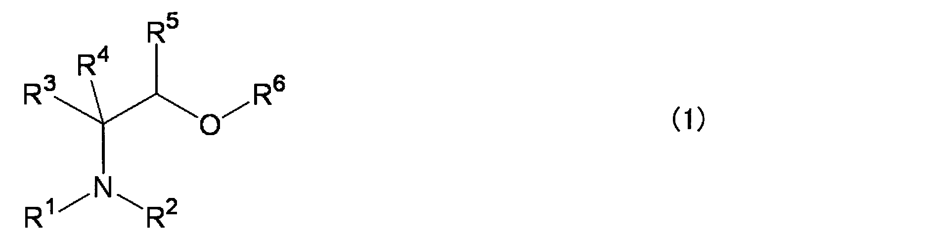
- 前記銅錯体(B)において、式(1)中、R6が水素原子であり、かつ、R1~R5のうち少なくとも1つがヒドロキシ基またはヒドロキシアルキル基である、請求項1に記載の導電膜形成用組成物。
- 前記銅錯体(B)において、式(1)中、R1およびR2のうち少なくとも1つがアルキル基である、請求項2に記載の導電膜形成用組成物。
- 前記銅錯体(B)において、銅の酸化数が+IIである、請求項1~3のいずれか1項に記載の導電膜形成用組成物。
- 前記銅錯体(B)がギ酸銅錯体である、請求項1~4のいずれか1項に記載の導電膜形成用組成物。
- 前記熱可塑性ポリマー(C)が親水性ポリマーである、請求項1~5のいずれか1項に記載の導電膜形成用組成物。
- 前記酸化銅粒子(A)が酸化銅(II)からなる、請求項1~6のいずれか1項に記載の導電膜形成用組成物。
- 前記熱可塑性ポリマー(C)がポリビニルピロリドン、ポリビニルアルコールおよびポリエチレンオキシドからなる群から選択される少なくとも1つである、請求項1~7のいずれか1項に記載の導電膜形成用組成物。
- 請求項1~8のいずれか1項に記載の導電膜形成用組成物を基材上に付与して、塗膜を形成する塗膜形成工程と、
前記塗膜に対して加熱および/または光照射による焼結処理を行い、導電膜を形成する導電膜形成工程と
を備える、導電膜の製造方法。 - 前記焼結処理がレーザー光照射またはパルス光照射により行われる、請求項9に記載の導電膜の製造方法。
Applications Claiming Priority (2)
| Application Number | Priority Date | Filing Date | Title |
|---|---|---|---|
| JP2013071935A JP2014196384A (ja) | 2013-03-29 | 2013-03-29 | 導電膜形成用組成物およびこれを用いる導電膜の製造方法 |
| JP2013-071935 | 2013-03-29 |
Publications (1)
| Publication Number | Publication Date |
|---|---|
| WO2014157303A1 true WO2014157303A1 (ja) | 2014-10-02 |
Family
ID=51624266
Family Applications (1)
| Application Number | Title | Priority Date | Filing Date |
|---|---|---|---|
| PCT/JP2014/058455 Ceased WO2014157303A1 (ja) | 2013-03-29 | 2014-03-26 | 導電膜形成用組成物およびこれを用いる導電膜の製造方法 |
Country Status (3)
| Country | Link |
|---|---|
| JP (1) | JP2014196384A (ja) |
| TW (1) | TW201444854A (ja) |
| WO (1) | WO2014157303A1 (ja) |
Families Citing this family (4)
| Publication number | Priority date | Publication date | Assignee | Title |
|---|---|---|---|---|
| JP2017001978A (ja) * | 2015-06-08 | 2017-01-05 | 国立大学法人北海道大学 | 銅錯体の製造方法およびこれを含有する導電膜形成用組成物 |
| JP7130631B2 (ja) * | 2017-05-18 | 2022-09-05 | 株式会社ダイセル | 導体の製造方法、配線基板の製造方法及び導体形成用組成物の製造方法 |
| EP3728492B1 (en) * | 2017-12-22 | 2022-08-17 | National Research Council of Canada | Copper ink for high conductivity fine printing |
| WO2022034755A1 (ja) * | 2020-08-13 | 2022-02-17 | 花王株式会社 | 金属ペースト |
Citations (8)
| Publication number | Priority date | Publication date | Assignee | Title |
|---|---|---|---|---|
| JPH1192256A (ja) * | 1997-09-19 | 1999-04-06 | Matsushita Electric Ind Co Ltd | 無機基板用導体、導体用ペースト及びこれを用いた無機多層基板 |
| JP2009158441A (ja) * | 2007-12-28 | 2009-07-16 | Namics Corp | 導電性ペースト及びそれを用いた銅膜の形成方法 |
| JP2009256218A (ja) * | 2008-04-14 | 2009-11-05 | Toray Ind Inc | 銅前駆体組成物およびそれを用いた銅膜の製造方法。 |
| JP2010176976A (ja) * | 2009-01-28 | 2010-08-12 | Tosoh Corp | 導電膜形成用組成物及びその製造方法、並びに導電膜の形成方法 |
| JP2010242118A (ja) * | 2009-04-01 | 2010-10-28 | Adeka Corp | 銅薄膜形成用組成物および該組成物を用いた銅薄膜の製造方法 |
| JP2012112022A (ja) * | 2010-11-26 | 2012-06-14 | Adeka Corp | 銅膜形成用組成物及び該組成物を用いた銅膜の製造方法 |
| JP2012151093A (ja) * | 2010-12-28 | 2012-08-09 | Tosoh Corp | 銅含有組成物、金属銅膜の製造方法、および金属銅膜 |
| JP2013510241A (ja) * | 2009-11-09 | 2013-03-21 | カーネギー メロン ユニバーシティ | 金属インク組成物、導電性パターン、方法および素子 |
Family Cites Families (6)
| Publication number | Priority date | Publication date | Assignee | Title |
|---|---|---|---|---|
| EP1626614B1 (en) * | 2003-05-16 | 2013-08-28 | Harima Chemicals, Inc. | Method for forming fine copper particle sintered product type of electric conductor having fine shape, method for forming fine copper wiring and thin copper film |
| JP2006096569A (ja) * | 2004-09-28 | 2006-04-13 | Fuji Photo Film Co Ltd | 銅酸化物微粒子の製造方法 |
| JP4606192B2 (ja) * | 2005-02-16 | 2011-01-05 | 旭化成イーマテリアルズ株式会社 | 回路板の製造方法 |
| JP5286846B2 (ja) * | 2008-03-12 | 2013-09-11 | 日立化成株式会社 | 導電性基板及びその製造方法、並びに銅配線基板及びその製造方法 |
| JP5730562B2 (ja) * | 2010-12-21 | 2015-06-10 | 三井金属鉱業株式会社 | 亜酸化銅粒子分散体 |
| JP2013008907A (ja) * | 2011-06-27 | 2013-01-10 | Hitachi Chem Co Ltd | 導電性ペースト用酸化銅粉末、導電性ペースト用酸化銅粉末の製造方法、導電性ペースト及びこれを用いて得られる銅配線層 |
-
2013
- 2013-03-29 JP JP2013071935A patent/JP2014196384A/ja active Pending
-
2014
- 2014-03-26 WO PCT/JP2014/058455 patent/WO2014157303A1/ja not_active Ceased
- 2014-03-27 TW TW103111352A patent/TW201444854A/zh unknown
Patent Citations (8)
| Publication number | Priority date | Publication date | Assignee | Title |
|---|---|---|---|---|
| JPH1192256A (ja) * | 1997-09-19 | 1999-04-06 | Matsushita Electric Ind Co Ltd | 無機基板用導体、導体用ペースト及びこれを用いた無機多層基板 |
| JP2009158441A (ja) * | 2007-12-28 | 2009-07-16 | Namics Corp | 導電性ペースト及びそれを用いた銅膜の形成方法 |
| JP2009256218A (ja) * | 2008-04-14 | 2009-11-05 | Toray Ind Inc | 銅前駆体組成物およびそれを用いた銅膜の製造方法。 |
| JP2010176976A (ja) * | 2009-01-28 | 2010-08-12 | Tosoh Corp | 導電膜形成用組成物及びその製造方法、並びに導電膜の形成方法 |
| JP2010242118A (ja) * | 2009-04-01 | 2010-10-28 | Adeka Corp | 銅薄膜形成用組成物および該組成物を用いた銅薄膜の製造方法 |
| JP2013510241A (ja) * | 2009-11-09 | 2013-03-21 | カーネギー メロン ユニバーシティ | 金属インク組成物、導電性パターン、方法および素子 |
| JP2012112022A (ja) * | 2010-11-26 | 2012-06-14 | Adeka Corp | 銅膜形成用組成物及び該組成物を用いた銅膜の製造方法 |
| JP2012151093A (ja) * | 2010-12-28 | 2012-08-09 | Tosoh Corp | 銅含有組成物、金属銅膜の製造方法、および金属銅膜 |
Also Published As
| Publication number | Publication date |
|---|---|
| JP2014196384A (ja) | 2014-10-16 |
| TW201444854A (zh) | 2014-12-01 |
Similar Documents
| Publication | Publication Date | Title |
|---|---|---|
| WO2014156594A1 (ja) | 導電膜形成用組成物およびこれを用いる導電膜の製造方法 | |
| JP5993812B2 (ja) | 導電膜の製造方法 | |
| CN104185880B (zh) | 液态组合物、金属铜膜和导体配线以及金属铜膜的制造方法 | |
| WO2014148091A1 (ja) | 導電膜形成用組成物およびこれを用いる導電膜の製造方法 | |
| CN104169462A (zh) | 液态组合物、金属膜和导体配线以及金属膜的制造方法 | |
| WO2014041956A1 (ja) | 導電層の製造方法、プリント配線基板 | |
| WO2015033823A1 (ja) | 導電膜の製造方法 | |
| WO2015015918A1 (ja) | 導電膜形成用組成物及び導電膜の製造方法 | |
| WO2014157303A1 (ja) | 導電膜形成用組成物およびこれを用いる導電膜の製造方法 | |
| JP2016058227A (ja) | 導電膜の製造方法 | |
| WO2014156326A1 (ja) | 導電膜形成用組成物およびこれを用いる導電膜の製造方法 | |
| JP5871762B2 (ja) | 導電膜形成用組成物および導電膜の製造方法 | |
| WO2014141787A1 (ja) | 導電膜形成用組成物及びこれを用いる導電膜の製造方法 | |
| JP2014167872A (ja) | 導電膜の製造方法、配線基板 | |
| WO2014156345A1 (ja) | 導電膜形成用組成物およびこれを用いる導電膜の製造方法 | |
| JP2014186952A (ja) | 被覆銅粒子の製造方法、導電膜形成用組成物の製造方法、導電膜の製造方法 | |
| WO2015005178A1 (ja) | 導電膜形成用組成物およびこれを用いる導電膜の製造方法 | |
| WO2014017288A1 (ja) | 導電膜形成用組成物および導電膜の製造方法 | |
| JP6263630B2 (ja) | 導電膜形成用組成物および導電膜形成方法 | |
| JP2014044907A (ja) | 導電膜形成用組成物および導電膜の製造方法 | |
| JP2016050246A (ja) | 導電膜形成用組成物 | |
| JP2015106523A (ja) | 導電膜形成用組成物 |
Legal Events
| Date | Code | Title | Description |
|---|---|---|---|
| 121 | Ep: the epo has been informed by wipo that ep was designated in this application |
Ref document number: 14773470 Country of ref document: EP Kind code of ref document: A1 |
|
| NENP | Non-entry into the national phase |
Ref country code: DE |
|
| 122 | Ep: pct application non-entry in european phase |
Ref document number: 14773470 Country of ref document: EP Kind code of ref document: A1 |