WO2014136602A1 - 窒化ガリウム結晶自立基板の製造方法 - Google Patents
窒化ガリウム結晶自立基板の製造方法 Download PDFInfo
- Publication number
- WO2014136602A1 WO2014136602A1 PCT/JP2014/054346 JP2014054346W WO2014136602A1 WO 2014136602 A1 WO2014136602 A1 WO 2014136602A1 JP 2014054346 W JP2014054346 W JP 2014054346W WO 2014136602 A1 WO2014136602 A1 WO 2014136602A1
- Authority
- WO
- WIPO (PCT)
- Prior art keywords
- gallium nitride
- nitride crystal
- main surface
- substrate
- crystal
- Prior art date
- Legal status (The legal status is an assumption and is not a legal conclusion. Google has not performed a legal analysis and makes no representation as to the accuracy of the status listed.)
- Ceased
Links
Images



Classifications
-
- C—CHEMISTRY; METALLURGY
- C30—CRYSTAL GROWTH
- C30B—SINGLE-CRYSTAL GROWTH; UNIDIRECTIONAL SOLIDIFICATION OF EUTECTIC MATERIAL OR UNIDIRECTIONAL DEMIXING OF EUTECTOID MATERIAL; REFINING BY ZONE-MELTING OF MATERIAL; PRODUCTION OF A HOMOGENEOUS POLYCRYSTALLINE MATERIAL WITH DEFINED STRUCTURE; SINGLE CRYSTALS OR HOMOGENEOUS POLYCRYSTALLINE MATERIAL WITH DEFINED STRUCTURE; AFTER-TREATMENT OF SINGLE CRYSTALS OR A HOMOGENEOUS POLYCRYSTALLINE MATERIAL WITH DEFINED STRUCTURE; APPARATUS THEREFOR
- C30B29/00—Single crystals or homogeneous polycrystalline material with defined structure characterised by the material or by their shape
- C30B29/10—Inorganic compounds or compositions
- C30B29/40—AIIIBV compounds wherein A is B, Al, Ga, In or Tl and B is N, P, As, Sb or Bi
- C30B29/403—AIII-nitrides
- C30B29/406—Gallium nitride
-
- C—CHEMISTRY; METALLURGY
- C30—CRYSTAL GROWTH
- C30B—SINGLE-CRYSTAL GROWTH; UNIDIRECTIONAL SOLIDIFICATION OF EUTECTIC MATERIAL OR UNIDIRECTIONAL DEMIXING OF EUTECTOID MATERIAL; REFINING BY ZONE-MELTING OF MATERIAL; PRODUCTION OF A HOMOGENEOUS POLYCRYSTALLINE MATERIAL WITH DEFINED STRUCTURE; SINGLE CRYSTALS OR HOMOGENEOUS POLYCRYSTALLINE MATERIAL WITH DEFINED STRUCTURE; AFTER-TREATMENT OF SINGLE CRYSTALS OR A HOMOGENEOUS POLYCRYSTALLINE MATERIAL WITH DEFINED STRUCTURE; APPARATUS THEREFOR
- C30B25/00—Single-crystal growth by chemical reaction of reactive gases, e.g. chemical vapour-deposition growth
- C30B25/02—Epitaxial-layer growth
- C30B25/18—Epitaxial-layer growth characterised by the substrate
- C30B25/186—Epitaxial-layer growth characterised by the substrate being specially pre-treated by, e.g. chemical or physical means
-
- H—ELECTRICITY
- H10—SEMICONDUCTOR DEVICES; ELECTRIC SOLID-STATE DEVICES NOT OTHERWISE PROVIDED FOR
- H10P—GENERIC PROCESSES OR APPARATUS FOR THE MANUFACTURE OR TREATMENT OF DEVICES COVERED BY CLASS H10
- H10P14/00—Formation of materials, e.g. in the shape of layers or pillars
- H10P14/20—Formation of materials, e.g. in the shape of layers or pillars of semiconductor materials
- H10P14/29—Formation of materials, e.g. in the shape of layers or pillars of semiconductor materials characterised by the substrates
- H10P14/2901—Materials
- H10P14/2921—Materials being crystalline insulating materials
-
- H—ELECTRICITY
- H10—SEMICONDUCTOR DEVICES; ELECTRIC SOLID-STATE DEVICES NOT OTHERWISE PROVIDED FOR
- H10P—GENERIC PROCESSES OR APPARATUS FOR THE MANUFACTURE OR TREATMENT OF DEVICES COVERED BY CLASS H10
- H10P14/00—Formation of materials, e.g. in the shape of layers or pillars
- H10P14/20—Formation of materials, e.g. in the shape of layers or pillars of semiconductor materials
- H10P14/34—Deposited materials, e.g. layers
- H10P14/3402—Deposited materials, e.g. layers characterised by the chemical composition
- H10P14/3414—Deposited materials, e.g. layers characterised by the chemical composition being group IIIA-VIA materials
- H10P14/3416—Nitrides
Definitions
- the present invention relates to a method for producing a high-quality gallium nitride (GaN) crystal free-standing substrate having a semipolar or nonpolar main surface, a large crystal layer thickness, a large area and high quality.
- GaN gallium nitride
- a semiconductor light emitting device such as a light emitting diode (LED) or a semiconductor laser (LD)
- multiple quantum devices in which a quantum well layer composed of an n-type GaN layer, an InGaN layer, and a barrier layer composed of a GaN layer are alternately stacked on a sapphire substrate.
- a well layer Multiple Quantum Wells: MQWs
- a p-type GaN layer are sequentially stacked are mass-produced.
- a GaN crystal grows in the axial direction, and its surface is a c-plane ( ⁇ 0001 ⁇ plane).
- an InGaN layer is formed on an a-plane ( ⁇ 11-20 ⁇ plane) or m-plane ( ⁇ 1-100 ⁇ plane), which is a nonpolar plane of a GaN crystal. It has been studied to avoid the influence of an internal electric field in which spontaneous polarization and piezoelectric polarization are superimposed (Patent Documents 1 to 3). Further, an InGaN quantum well layer is formed on a surface called a semipolar surface inclined in the a-axis or m-axis direction, for example, a semipolar ⁇ 11-22 ⁇ surface, where the c-plane which is a polar surface, It is also studied to avoid the influence of the internal electric field (Non-patent Documents 1 and 2).
- crystal dislocations are generated from the interface between sapphire and GaN due to a difference in lattice constant between sapphire as a base substrate and GaN as a growth crystal.
- homoepitaxial growth in which a GaN crystal layer is grown on a GaN crystal substrate is effective.
- the base substrate and the growth layer are the same material, it is possible to suppress the occurrence of dislocation due to the difference in physical properties. For this reason, a GaN crystal free-standing substrate is required to perform homoepitaxial growth.
- a GaN crystal free-standing substrate having a nonpolar plane and a semipolar plane as a main surface is useful for manufacturing a highly efficient semiconductor light emitting device.
- GaN crystal free-standing substrates having a nonpolar plane and a semipolar plane as a main surface are not in circulation and are difficult to obtain. The reason is as follows.
- As a method for producing a GaN crystal free-standing substrate having a nonpolar plane and a semipolar plane as a main surface there is a method of cutting a specific surface from a bulk GaN crystal as a main surface, but the cost becomes extremely high, and a large area However, it is not accepted industrially.
- Non-patent Document 3 a technique for masking a ⁇ 11-22 ⁇ plane GaN crystal surface formed from a flat sapphire base substrate having a ⁇ 1010 ⁇ plane and further forming a GaN crystal layer thereon is disclosed.
- the thickness of the GaN crystal layer to be formed is thin and is not related to a GaN crystal free-standing substrate (Non-patent Document 3).
- the inventors of the present application applied a GaN crystal having a c-plane of about 3 mm thickness as a main surface by a HVPE method on the surface of a GaN crystal layer having a ⁇ 0001 ⁇ plane formed on a flat sapphire base substrate having a ⁇ 0001 ⁇ plane.
- a method for manufacturing free-standing substrates Developed a method for manufacturing free-standing substrates.
- a semipolar or nonpolar GaN crystal self-supporting substrate was manufactured by the same method, cracks occurred, and in extreme cases, tearing occurred, or even if not cracked, the surface smoothness was poor and the thickness was large. A high-quality, large-area free-standing substrate could not be manufactured.
- the inventors of the present invention use a processed substrate in which specific grooves are formed as a sapphire base substrate for crystal growth by the MOVPE method when a GaN crystal free-standing substrate is manufactured by combining the MOVPE method and the HVPE method.
- the surface is semi-polar with a large and smooth surface with no cracks or cracks and a thickness of several millimeters.
- the inventors have found that a nonpolar GaN crystal free-standing substrate can be manufactured, and have completed the present invention.
- a gallium nitride crystal layer having a semipolar or nonpolar main surface is grown on a sapphire base substrate on which a plurality of grooves having sidewalls inclined with respect to the main surface of the base substrate are formed,
- a gallium nitride crystal layer having a semipolar or nonpolar main surface having a thickness of 0.05 to 5 ⁇ m is formed on the sapphire base substrate by metal organic vapor phase epitaxy (MOVPE).
- MOVPE metal organic vapor phase epitaxy
- nitriding with a semipolar or nonpolar main surface of 0.2 to 5 mm thickness is performed on the crystal layer surface by a hydride vapor phase epitaxy (HVPE) method.
- HVPE hydride vapor phase epitaxy
- the formed gallium nitride crystal layer has a plurality of crystal association portions formed by crystal growth from the groove portion of the sapphire base substrate, and masking is one of the crystal association portions existing on the surface of the gallium nitride crystal layer. It is particularly suitable to mask the part, 2) 10 to 90% of the growth surface of the gallium nitride crystal layer formed by MOVPE is covered by masking, and 20% to 80% of the crystal association part existing on the surface of the gallium nitride crystal layer is covered.
- the mask used for masking has a stripe shape 4)
- the mask used for masking has a lattice shape 5)
- the mask used for masking has a dot shape 6)
- the ratio of the total area of the side wall that is the starting point of crystal growth is 1 to 20% of the total surface area of the base substrate on the side on which the gallium nitride crystal layer is formed.
- the gallium nitride crystal free-standing substrate having a ⁇ 0001 ⁇ plane is a gallium nitride crystal free-standing substrate having a main surface inclined by 1 ° to 90 ° toward the ⁇ 10-10> axis direction; 8) A gallium nitride crystal free-standing substrate having a semipolar or nonpolar main surface, the ⁇ 0001 ⁇ plane having a main surface inclined by 1 ° to 90 ° toward the ⁇ 11-20> axis direction Being a self-supporting substrate, 9)
- the dark spot density of the gallium nitride crystal free-standing substrate is less than 2 ⁇ 10 8 pieces / cm 2 . 10) It is preferable that the RMS (surface roughness) of the gallium nitride crystal surface at the time of removal from the crystal growth furnace after crystal formation by the HVPE method is less than 300 nm.
- the method for manufacturing a semipolar or nonpolar plane GaN crystal free-standing substrate combining the MOVPE method and the HVPE method of the present invention, it is possible to provide a GaN crystal free-standing substrate with few cracks and defects and no surface irregularities. That is, according to the present invention, the dark spot density is less than 2 ⁇ 10 8 pieces / cm 2 , the thickness is 0.2 to 5 mm, the as-grown crystal surface has an RMS of less than 300 nm, and is semipolar or nonpolar.
- a large-area GaN crystal free-standing substrate having a characteristic plane orientation can be provided at low cost.
- the substrate and the growth layer are the same because the materials of the base substrate and the growth layer are the same. Generation of dislocations can be suppressed, and a semiconductor light emitting device with high luminous efficiency can be manufactured. Furthermore, since the surface orientation of the surface of the GaN crystal layer is a nonpolar plane or a semipolar plane, there is an effect of a decrease in light emission efficiency due to the quantum confined Stark effect compared to a conventional GaN crystal layer substrate having a c-plane as a main surface. small.
- the method of the present invention is more advantageous as the area of the crystal growth layer is larger, and the area of the obtained crystal is 1 cm 2 or more, preferably 5 cm 2 or more, more preferably 10 cm 2 or more. It is suitable for manufacturing a GaN crystal free-standing substrate having an area.
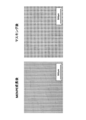
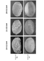
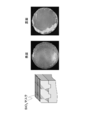
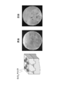
- Example 1 is a schematic diagram of a mask (stripes) used, and photographs of the front and back surfaces of the generated free-standing GaN crystal. It is the schematic diagram of the mask (stripe) used in Example 9, and the photograph of the surface and back surface of the produced
- the method for producing a semipolar or nonpolar GaN crystal free-standing substrate high-crystalline crystal growth is performed by MOVPE on a sapphire base substrate on which a plurality of grooves having inclined sidewalls are formed, and then masked. Thereafter, since high-speed crystal growth is further performed by the HVPE method, the generation of cracks is suppressed, the defect density (dark spot density) is small, and the smoothness of the crystal surface is excellent.
- the dark spot density is a physical property value serving as an index for indicating the density of threading dislocations, which are dislocation defects in the crystal, and is measured using a scanning electron microscope / cathode luminescence (SEM / CL) apparatus.
- the acceleration voltage during measurement is 5 kV, and the observation range is 20 ⁇ m ⁇ 20 ⁇ m.
- the dark spot density is calculated from the total number of dark spots observed within the observation range.
- semipolar and nonpolar may be collectively referred to as nonpolar.
- the base substrate used in the present invention is a substrate made of sapphire, and the main surface of the sapphire base substrate has an arbitrary plane orientation selected according to the crystal plane of the target GaN crystal.
- the ⁇ 0001 ⁇ plane of the GaN crystal has a main surface inclined by 1 ° to 90 ° toward the ⁇ 10-10> axial direction, or the ⁇ 0001 ⁇ plane of the GaN crystal extends in the ⁇ 11-20> axial direction.
- a gallium nitride crystal self-supporting substrate having a main surface inclined by 1 ° to 90 ° as a main surface is a preferable manufacturing object in terms of avoiding an internal electric field in forming an InGaN layer.
- the c-axis of sapphire and the c-axis of GaN crystal are aligned, and the m-axis of sapphire and the a-axis of GaN crystal are aligned.
- sapphire having a miscut surface inclined by a corresponding angle is used.
- each of the principal planes is ⁇ 1-
- a sapphire base substrate having a 100 ⁇ plane and a ⁇ 11-20 ⁇ plane is used.
- the main surface of the sapphire base substrate is the r plane ( ⁇ 10-12 ⁇ plane).
- the main surface of the sapphire base substrate is an n-plane ( ⁇ 11-23 ⁇ plane).
- the main surface of the sapphire base substrate is a ⁇ 22-43 ⁇ plane.
- a sapphire base substrate having a ⁇ 20-21 ⁇ plane as a main surface can be used.
- the base substrate is usually a disc having a thickness of 0.3 to 3.0 mm and a diameter of 50 to 300 mm, but is not particularly limited thereto.
- the sapphire base substrate is a substrate having a main surface as described above, and has a plurality of grooves as shown in FIG. 1, and a part of the side walls of the grooves is the starting point of crystal growth. It is essential to use a base substrate (groove portion-formed sapphire base substrate) having a groove portion that can become a groove. By using the base substrate, the crystal quality can be improved, and the base substrate and the GaN crystal layer can be separated by a simple operation by cooling in a later process.
- the base substrate main surface is the ⁇ 10-12 ⁇ plane and the extending direction of the groove is the ⁇ 11-20 ⁇ plane, that is, the a-axis direction
- the c-plane is formed on one side wall of the groove.
- the base substrate principal surface is the ⁇ 11-23 ⁇ plane and the extending direction of the groove is the ⁇ 10-10 ⁇ plane, that is, the m-axis direction
- a c-plane is formed on one side wall of the groove.
- a crystal grows by selective lateral growth (ELO) starting from a side wall as a growth starting point.
- the side wall preferably has a total area of 1 to 20% with respect to the total surface area of the base substrate on the side where the gallium nitride crystal layer is formed.
- the opening width of the groove is not particularly limited, and is usually set in the range of 0.5 to 10 ⁇ m.
- the interval between the groove portions that is, the interval between the groove portions adjacent to each other on the main surface of the base substrate is 1 to 100 ⁇ m.
- the depth of the groove is generally 1 to 1000 ⁇ m.
- the number of grooves on the main surface can be arbitrarily set according to the desired area of the GaN crystal to be formed, but usually taking into account the opening width, the interval between the grooves, and the width of the bottom surface, About 10 to 500 may be provided.
- the groove has a side wall inclined at a predetermined angle with respect to the main surface of the base substrate.
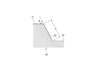
- the cross-sectional shape narrows the groove width from the groove opening toward the groove bottom.
- the taper is sloping.
- the inclination angle means an angle ( ⁇ ) formed by the base substrate main surface and the extended surface of the groove side wall. The angle is determined in consideration of the surface orientation of the side wall surface formed corresponding to the surface orientation of the base substrate main surface.
- this angle ( ⁇ ) is set to 58.4 degrees.
- a GaN crystal is grown so that the c-axis of the GaN crystal is in the same direction as the c-axis of the sapphire base substrate to obtain a desired crystal.
- the angle 58.4 degrees at this time is formed by the ⁇ 11-22 ⁇ plane that is the principal surface of the desired GaN crystal and the c-plane of the GaN crystal that is perpendicular to the c-axis of the GaN crystal that is the growth direction. Depends on the angle being 58.4 degrees.
- the angle formed by the ⁇ 10-12 ⁇ plane, which is the main surface of the sapphire base substrate, and the sapphire c-plane appearing on the side wall of the groove is 57.6 degrees, so the surface of the GaN crystal layer grown thereon is Inclined about 0.8 degrees with respect to the main surface of the sapphire base substrate.
- the ⁇ 11-22 ⁇ plane of the GaN crystal is a sapphire base substrate.
- a GaN crystal layer grown so as to be parallel to the main surface can be obtained.
- this angle is set to 62.0 degrees.
- a miscut substrate that is a surface with an off-angle so as to cancel out the tilt angle between the main surface of the base substrate of about 0.8 degrees and the surface of the GaN crystal, which occurs for the same reason as described above,
- a GaN crystal layer grown so that the ⁇ 10-11 ⁇ plane is parallel to the principal surface of the sapphire base substrate can be obtained.
- the surface orientation of the main surface of the sapphire base substrate is ⁇ 22-43 ⁇ and the desired surface orientation of the GaN crystal is the ⁇ 20-21 ⁇ plane, this angle is set to 75.1 degrees.
- a miscut substrate that is a surface with an off-angle so as to cancel out the inclination angle between the base substrate main surface of about 0.5 degrees and the GaN crystal surface, which occurs for the same reason as described above, a GaN crystal A GaN crystal layer grown so that its ⁇ 20-21 ⁇ plane is parallel to the principal surface of the sapphire base substrate can be obtained.
- the surface orientation of the main surface of the sapphire base substrate is ⁇ 11-20 ⁇ and the surface orientation of the desired GaN crystal is the ⁇ 10-10 ⁇ plane, or the surface orientation of the main surface of the sapphire base substrate is ⁇ 10-10] ⁇
- this angle is set to 90 degrees, and the GaN crystal is separated from the c-axis of the sapphire base substrate and the c-axis of the GaN crystal from this side wall. Are grown in the same direction to obtain a desired crystal.
- the angle ( ⁇ ) formed by the base substrate main surface and the groove side wall of 90 ° is difficult.
- the ⁇ 10-10 ⁇ plane of the GaN crystal is on the sapphire base substrate main surface on the sapphire base substrate having the ⁇ 11-20 ⁇ plane as the main surface.
- a GaN crystal layer grown so as to be obtained can be obtained.
- this angle is set to 90 degrees and GaN is A desired crystal is obtained by growing so that the c-axis of the GaN crystal is in the same direction as the c-axis of the sapphire base substrate.
- the width (d) of the GaN crystal growth region (hereinafter referred to as the crystal growth region) on the side wall of the groove is not particularly limited, but is preferably 0.01 to 3 ⁇ m in order to reduce the dark spot density.
- the thickness is particularly preferably 0.1 to 1 ⁇ m.
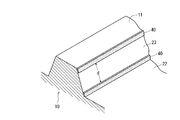
- the width (d) of the crystal growth region is defined between the side where the base substrate main surface and the side wall intersect and the side where the side wall and the groove bottom face intersect when all the side walls are crystal growth regions.
- the shortest distance (interval) on the side wall As shown in FIG. 3, when a part of the side wall is masked and the crystal growth region is limited, the distance (d) is obtained by subtracting the width of the masking portion from the shortest distance (interval).
- the groove portion having the sidewall having the predetermined inclination angle is formed by patterning a photoresist so that only a portion where the groove portion is to be formed becomes an opening, the photoresist is used as an etching resist, and the sapphire base substrate is subjected to reactive ion etching (Reactive Ion It can be formed by dry etching such as Etching (RIE) or wet etching.
- reactive Ion etching reactive ion etching
- control means such as the width of the side wall, the width of the groove opening, the space between the grooves, and the width of the bottom surface, the photoresist coating amount, baking temperature, baking time, UV irradiation amount, UV, Examples include the shape of a photomask when irradiating.
- the etching stage it can be controlled by the etching gas type, etching gas concentration, etching gas mixture ratio, antenna power, bias power, etching time, and the like. By combining these various conditions, a sapphire base substrate having a groove having a predetermined shape can be obtained.
- the width of the side wall can be controlled by obtaining an etching rate, which is the rate at which sapphire is etched per unit time, and changing the etching time.
- a base substrate having side walls of various plane orientations can be created by selecting the main surface of the sapphire base substrate and setting the direction in which the groove extends. Specifically, when the base substrate main surface is the ⁇ 10-12 ⁇ plane and the extending direction of the groove is the ⁇ 11-20 ⁇ plane orientation, that is, the a-axis direction, The c-plane is exposed. When the base substrate principal surface is the ⁇ 11-23 ⁇ plane and the extending direction of the groove is the ⁇ 10-10 ⁇ plane orientation, that is, the m-axis direction, the c-plane is exposed on the side wall which is the crystal growth plane. .
- the base substrate main surface is the ⁇ 11-20 ⁇ plane and the extending direction of the groove is the ⁇ 10-10 ⁇ plane orientation, that is, the m-axis direction
- the c-plane is exposed on the side wall that is the crystal growth plane.
- the base substrate main surface is the ⁇ 10-10 ⁇ plane and the extending direction of the groove is the ⁇ 11-20 ⁇ plane orientation, that is, the a-axis direction
- the c-plane is exposed on the side wall that is the crystal growth surface.
- the base substrate main surface is the ⁇ 22-43 ⁇ plane and the extending direction of the groove is the ⁇ 10-10 ⁇ plane orientation, that is, the m-axis direction
- the c-plane is exposed on the side wall as the crystal growth plane. .
- the sapphire base substrate can be arbitrarily designed with respect to the surface orientation of its main surface and the surface orientation of the side wall that becomes the crystal growth starting surface.
- the sidewalls having various plane orientations lateral growth starting from the c-plane sidewall is likely to occur preferentially and easily controlled. Therefore, it is a preferable aspect to form a side wall composed of the c-plane on at least a part of the side wall constituting the groove.
- a high-quality semipolar or nonpolar GaN crystal is grown on the sapphire base substrate by the MOVPE method. Its thickness is 0.05 to 5 ⁇ m. When the thickness is less than 0.05 ⁇ m, the dark point density of the obtained crystal is large, and high-quality crystals cannot be obtained by subsequent crystal growth, and growth exceeding 5 ⁇ m results in poor growth efficiency.
- the growth temperature and growth are controlled in order to control the growth from the side walls of the groove without causing growth from the main surface of the substrate. It is necessary to optimize various conditions such as pressure, raw material gas supply amount, raw material gas supply ratio, carrier gas type, carrier gas amount, etc. The conditions should be determined by preliminary experiments. Specifically, when the base substrate main surface is a ⁇ 10-12 ⁇ plane, a ⁇ 11-23 ⁇ plane, or a ⁇ 22-43 ⁇ plane, the GaN crystal is exposed, and the main substrate main plane and the sapphire c plane are exposed. There is a possibility of crystal growth from the groove side wall and the other side wall of the groove.
- the growth from the main surface of the base substrate can be suppressed by forming and providing a crystal growth inhibiting layer.
- the base substrate main surface is a ⁇ 11-20 ⁇ plane or a ⁇ 10-10 ⁇ plane
- the GaN crystal may grow from the base substrate main surface and the groove side wall.
- the groove side walls on both sides have the same plane orientation, it is necessary to control so that the GaN crystal having the same plane orientation grows from either side and the crystal grows from either side wall of the trench.
- the growth from the main surface of the base substrate may be suppressed. In order to suppress the growth from the main surface of the base substrate, formation of a crystal growth inhibiting layer is effective, but control is possible only by optimizing the above various growth conditions.
- GaN crystals grow and grow from a plurality of c-planes exposed in the groove portions of the sapphire base substrate, GaN crystals grown from adjacent groove portions associate to form a crystal association portion.
- the crystal association part appears in a linear shape.
- Each GaN crystal has a slight axial misalignment and a slight strain difference, so that a defect occurs in the crystal association part.
- the defects propagate to the crystal surface. This is a phenomenon that cannot be controlled by optimizing crystal growth conditions.
- the GaN crystal layer is formed on the groove-forming sapphire base substrate by the MOVPE method
- a part of the growth surface of the GaN crystal layer is masked, and then the GaN crystal is formed by the HVPE method. It is important to grow.
- Masking is not effective in suppressing the occurrence of cracks even if crystal growth is performed by directly performing masking on the groove-formed sapphire base substrate. This is because micronucleation and dislocation generation regions are already controlled by the groove formation. This method does not contribute to the generation of cracks in the GaN layer formed by HVPE growth and the improvement of surface flatness.
- masking is performed on the GaN crystal layer formed in advance by the MOVPE method, thereby preventing the influence of partial surface misalignment and axial misalignment of the GaN crystal layer and suppressing the occurrence of cracks.
- the suppression mechanism is considered to be influenced by controlling the growth direction by performing ELO growth only from a predetermined opening and preventing abnormal growth with different growth directions and orientations.
- the mask part acts as a buffer layer that absorbs the thermal expansion difference between the groove-formed sapphire base substrate and the GaN crystal by masking, and suppresses the generation of cracks in the GaN crystal formed above. Get it.
- the masking may be performed on a part of the surface of the GaN crystal layer, but it is particularly preferable to mask a part of the crystal association part existing on the surface of the GaN crystal layer. That is, by masking a part of the surface of the crystal association part, the strain accumulated in the defect is dispersed and released. As a result, it is possible to effectively reduce cracks generated in the GaN crystal that is subsequently grown by the HVPE method. However, it is more preferable that the masking is not performed on all the crystal association parts. If the entire defect surface of the crystal association part is masked, the strain accumulated in the defect is not dispersed and released, and there is a risk that cracks are likely to occur in the GaN crystal grown thereon.
- Masking means is known per se, a vacuum deposition, sputtering, by a method such as CVD (Chemical Vapor Deposition), the underlying substrate surface, the thermal expansion coefficient small compared to the sapphire and GaN crystal, SiO 2 film, SiN x
- Examples of the method include masking by forming a film, a TiO 2 film, a ZrO 2 film, or the like.
- the thickness of the masking layer is usually about 0.001 to 3 ⁇ m.
- the masking ratio (growth surface mask coverage) on the surface of the GaN crystal layer formed by the MOVPE method is usually preferably 10 to 90% with respect to the total surface area of the crystal growth surface on the substrate.
- the area of the meeting part existing on the surface of the GaN crystal layer is calculated from the sum of the products of the width and the length of the meeting part of the dark spot existing in the observation range by the SEM / CL apparatus.
- the mask shape of the mask is not particularly limited as long as the surface of the GaN crystal layer is covered. As shown in FIG. 4, a stripe mask, a lattice mask, a dot mask, a honeycomb mask, etc. Various shapes are adopted.
- the grids of the grid-like mask may be orthogonal or may cross at a predetermined angle.
- the shape of the dot is not particularly limited, and specific examples include a circle, a triangle, a square, and a hexagon. It is preferable that the units constituting the mask, for example, the lines in the case of the stripe-shaped mask and the dots in the case of the dot-shaped mask exist at equal intervals.
- the unit may be a single unit or a plurality of aggregates.
- the number of lines constituting the striped mask may be one or a combination of a plurality of lines.
- the target crystal plane orientation of GaN plane orientation of the sapphire base substrate used
- ⁇ 0001 ⁇ plane ⁇ 0001 ⁇ plane
- it has six-fold symmetry in the plane orientation in the growth plane. Even if any of the above masks is used, it hardly affects the generation of cracks or crystal cracks. That is, the dependence on the mask shape is small.
- the crystal plane orientation of GaN (plane orientation of the sapphire base substrate used) is ⁇ 11-22 ⁇ plane ( ⁇ -1012 ⁇ plane), ⁇ 10-11 ⁇ plane ( ⁇ 11-23 ⁇ plane), ⁇ 20 In the case of the ⁇ 21 ⁇ plane ( ⁇ 22-43 ⁇ plane), etc., it has two orthogonal axes of symmetry within the plane orientation of the growth plane, and the difference in the coefficient of thermal expansion between each axis is noticeable. Since the generation of cracks is likely to occur, a mask that can disperse and relax strains from multiple directions is preferable. From this point, a dot-shaped mask with circular dots is particularly preferable.
- the diameter of the dot means the diameter of the circumscribed circle of each dot other than a circle.
- the diameter is 0.1 to 100 ⁇ m
- the distance between the center of a dot and the center of an adjacent dot is 0.2 to 200 ⁇ m
- a mask in which these dots are regularly arranged is preferably used.
- the dot diameter is less than 0.1 ⁇ m, the effect on the smooth structure of the crystal surface tends to be reduced.
- the dot diameter exceeds 100 ⁇ m, the possibility of abnormal growth from the mask increases and a polycrystal tends to be formed. It is in.
- the distance between the center of a certain dot and the center of an adjacent dot is less than 0.2 ⁇ m, the effect of reducing the defect density in selective lateral growth tends to be reduced. Similarly, when it exceeds 200 ⁇ m, the effect of reducing the defect density tends to be reduced.
- the mask width (short axis width) of the stripe is usually 0.5 to 500 ⁇ m, and the opening width (interval between stripes) is usually 0. 5 to 50 ⁇ m. If the mask width of the stripe is less than 0.5 ⁇ m, the effect on the smooth structure of the crystal surface tends to be reduced, and if it exceeds 500 ⁇ m, the possibility of abnormal growth from the mask increases, resulting in a polycrystal. There is a tendency. On the other hand, when the opening width is less than 0.5 ⁇ m, the effect of reducing the defect density in selective lateral growth tends to be reduced. Similarly, when the thickness exceeds 50 ⁇ m, the effect of reducing the defect density tends to be reduced.
- the sapphire base substrate used in the present invention is a single crystal, and has various crystal main surfaces as described above corresponding to the crystal orientation of the target GaN crystal. Therefore, the substrate has two different thermal expansion coefficients that are orthogonal to each other. Therefore, by forming a striped mask in parallel with the direction of large thermal expansion, the strain applied between the GaN crystal layer and the groove-formed sapphire base substrate can be buffered, and as a result, the GaN crystal formed by the HVPE method can be buffered. Breaking can be prevented.
- a part of the surface of the semipolar or nonpolar GaN crystal layer formed by the MOVPE method is subjected to the masking treatment as described above, and then a high-speed crystal is formed thereon by the HVPE method.
- the HVPE method is a method in which gallium chloride and ammonia as a nitrogen source are reacted in a gas phase to epitaxially grow a GaN crystal on a base substrate, and is a method known per se.
- the HVPE apparatus used for crystal growth is mainly composed of a reaction tube, a heating system, a gas supply system, and a gas exhaust system.
- the gas supply system can precisely control the gas supply amount by a mass flow controller.
- a hot wall method is used in which a reaction tube made of quartz is covered with a resistance heating heater, and the reaction tube, a substrate and a susceptor installed therein, and a metal material are heated.
- the source gas can be sufficiently heated and supplied to the substrate surface, and the saturated vapor pressure of the supplied source can be increased. As a result, a large amount of raw material can be supplied and high-speed growth can be realized.
- the reaction tube is roughly divided into a metal raw material part and a substrate heating part.
- Ga metal is placed in the metal raw material portion, and by supplying HCl gas at a high temperature, Ga metal reacts with HCl gas to generate GaCl.
- the generated GaCl gas passes through a quartz pipe and is carried to the substrate heating unit.
- a susceptor made of carbon or SiC is arranged perpendicular to the gas flow, and the susceptor has a rotation mechanism. Then, a sapphire base substrate or a laminated substrate in which a GaN crystal is grown on the sapphire base substrate is set on the susceptor, and the GaCl gas generated in the metal raw material part and the NH 3 gas react on the substrate.
- the growth of the GaN crystal proceeds.
- NH 3 gas as a nitrogen source and HCl gas for generating GaCl as a Ga source are used as source gases.
- Cl 2 gas may be used instead of HCl gas.
- Ga metal which is a Ga raw material is installed in the apparatus.
- Carrier gases such as H 2 and N 2 are used in addition to the source gas NH 3 and HCl gas.
- the GaN crystal having excellent surface smoothness can be obtained when the GaN crystal surface is taken out of the crystal growth furnace after the HVPE method, that is, the RMS of the as-grown gallium nitride crystal surface is less than 300 nm, preferably less than 30 nm. .
- a GaN free-standing substrate is obtained by separating the base substrate by a known method such as laser irradiation separation or polishing.
- a known method such as laser irradiation separation or polishing.
- methods such as laser irradiation separation and polishing may cause damage to the GaN crystal, and are not necessarily efficient separation methods.
- the substrate is cooled. Separation occurs due to spontaneous peeling at the interface between the sapphire base substrate and the GaN crystal layer only by stress.
- the cooling may be performed forcibly by supplying a low temperature gas or the like, or may be performed by natural cooling.
- the temperature of the sapphire base substrate and the GaN crystal layer is lowered to 20 ° C. to 150 ° C. by cooling.
- the cooling rate is, for example, 1 to 100 ° C./min.
- Example 1 [Formation of GaN crystal layer] A resist was patterned in a stripe shape on a ⁇ 10-12 ⁇ plane sapphire substrate, and then dry etching was performed by reactive ion etching (RIE) to form a plurality of grooves on the sapphire substrate.
- the groove portion was formed so that the groove opening width was 3 ⁇ m, the groove depth was 1 ⁇ m, and the width of the substrate main surface portion to the adjacent groove portion was 3 ⁇ m. After dry etching, the resist was removed by washing to obtain a groove-formed sapphire base substrate.
- RIE reactive ion etching
- This groove-forming sapphire base substrate has a substrate main surface (2 inches ⁇ ), a surface-exposed crystal growth region (C surface) composed of a plurality of grooves formed on the substrate main surface, and a groove bottom surface.
- the temperature of the substrate is set to 460 ° C.
- the pressure in the reaction vessel is set to 100 kPa
- the carrier gas H 2 flowing through the reaction vessel is allowed to flow at a flow rate of 5 L / min. NH 3 ) and a group III element supply source (TMG) were supplied at a rate of 5 L / min and 5.5 ⁇ mol / min, respectively, and about 25 nm of GaN on the amorphous was deposited on the substrate.
- TMG group III element supply source
- the temperature of the substrate is set to 1025 ° C.
- the pressure in the reaction vessel is set to 20 kPa
- the carrier gas flowing in the reaction vessel is set to H 2
- the flow rate is 5 L / min.
- the GaN deposited on was recrystallized to selectively form GaN crystal nuclei in the crystal growth region on the side wall of the groove. Subsequently, the temperature of the substrate is set to 1075 ° C., the pressure in the reaction vessel is set to 20 kPa, and the carrier gas to be circulated in the reaction vessel is set to H 2 while being circulated at a flow rate of 5 L / min.
- a resist was spin-coated on the prepared GaN crystal layer (growth surface). Subsequently, the resist was patterned in a stripe shape in a direction of 90 ° with respect to the groove portion of the sapphire substrate by photolithography. Next, a SiO 2 film having a thickness of 100 nm was formed by sputtering. After the film formation, the resist was washed away to form an SiO 2 layer having a plurality of stripes on the GaN crystal layer. The stripe width was 3 ⁇ m, the mask height was 100 nm, and the opening width was 3 ⁇ m.
- the ratio of masking to the GaN crystal growth surface that is, “growth surface mask coverage” and “association surface mask coverage” are defined as follows, and were calculated as follows.
- “Growth surface mask coverage” (Total area of mask portion / area of GaN crystal surface) ⁇ 100
- “Surface mask coverage of meeting part” (Masking area of the association part existing on the surface of the GaN crystal layer / Total area of the crystal association part existing on the surface of the GaN crystal layer on the crystal surface) ⁇ 100
- the area of the GaN crystal surface is the area of the base substrate, and the total area of the mask portion on the surface is obtained from the interval between the stripe width and the opening width.
- the “growth surface mask coverage” is 50%.
- the total area of the crystal association part on the GaN crystal surface is 1.01 cm 2
- the total area of the masking part on the association part surface is 0.50 cm 2 . Therefore, the “association part surface mask coverage” is 50%.
- the prepared GaN crystal with mask is set on a carbon material fixing base so that the mask faces the upstream of the gas in the HVPE apparatus, and then N 2 gas is circulated in the reaction tube for 30 minutes, and the reaction tube is placed in an N 2 gas atmosphere. It was.
- the reaction tube was heated so that the metal raw material portion was 850 ° C. and the substrate heating portion was 1100 ° C., and was held for 25 minutes after reaching the set temperature. At this time, until the substrate heating portion reaches 500 ° C. was circulated in N2 gas into the reaction tube, H 2 gas at 500 ° C. or higher, and was passed through the NH 3 gas.
- HCl gas was passed through the Ga metal installed in the reaction tube at 1.2 L / min. Further, NH 3 gas was supplied at 36 L / min and carrier gas H 2 gas was supplied at 4.1 L / min, and a GaN crystal was grown for 240 minutes. The film thickness of the GaN crystal was 2500 ⁇ m. Thereafter, the flow of HCl gas was stopped, the growth was terminated, and the substrate was cooled. Cooling was performed by natural cooling while circulating gas. During cooling, NH 3 gas was circulated at 5 L / min until the substrate temperature was 600 ° C. or lower, and N 2 gas was circulated at 37.7 L / min at 600 ° C. or lower. When the substrate temperature is 150 ° C. or lower, the substrate is taken out from the apparatus. At that time, the sapphire base substrate and the GaN crystal layer are already separated in an area of 50% or more, and are not separated. The SUS tweezers could be easily peeled off.
- the characteristics of the obtained GaN crystal free-standing substrate were measured by the following method.
- the obtained crystal was a self-standing GaN substrate having a ⁇ 11-22 ⁇ plane as a main surface, a thickness of 2500 ⁇ m, and an RMS of less than 300 nm. No cracks could be confirmed on the front side. A part of the sapphire of the base substrate adhered to the back side, but it separated spontaneously without cracking and consisted only of GaN crystals. The dark spot density was 4.09 ⁇ 10 5 pieces / cm 2 .
- Example 2 The GaN crystal layer was formed in the same manner as in Example 1. Subsequently, a dot-shaped mask made of SiO 2 having a height of 100 nm in which circles having a diameter of 3 ⁇ m were arranged at the vertices of an equilateral triangle having a side of 5 ⁇ m in plan view on the GaN crystal growth surface was formed. Next, a GaN thick film is formed in the same manner as in Example 1 to obtain a self-standing GaN substrate having an equivalent area with a ⁇ 11-22 ⁇ plane as the main surface, a thickness of 2500 ⁇ m, and an RMS of less than 300 nm. It was. There was one crack on the front side. A part of the sapphire of the base substrate adhered to the back side, but it was separated spontaneously and consisted of only GaN crystals. The dark spot density was 9.02 ⁇ 10 5 pieces / cm 2 .
- Example 3 The GaN crystal layer was formed in the same manner as in Example 1. Subsequently, a stripe mask made of SiO 2 was formed at an angle parallel to the groove on the sapphire substrate. The stripe width, opening width, and mask height were the same as in Example 1. Next, a GaN thick film was formed in the same manner as in Example 1 to obtain a self-standing GaN substrate having a ⁇ 11-22 ⁇ plane as a main surface, a thickness of 2500 ⁇ m, and an RMS of less than 300 nm. No cracks could be confirmed on the front side. A part of the sapphire of the base substrate adhered to the back side, but it separated spontaneously without cracking and consisted only of GaN crystals. The dark spot density was 2.14 ⁇ 10 6 pieces / cm 2 .
- Example 4 The GaN crystal layer was formed in the same manner as in Example 1. Subsequently, a stripe mask made of SiO 2 was formed at an intersecting angle of 1 ° with the groove on the sapphire substrate. The stripe width, opening width, and mask height were the same as in Example 1. Next, a GaN thick film was formed in the same manner as in Example 1 to obtain a self-standing GaN substrate having a ⁇ 11-22 ⁇ plane as a main surface, a thickness of 2500 ⁇ m, and an RMS of less than 300 nm. No cracks could be confirmed on the front side. A part of the sapphire of the base substrate adhered to the back side, but it separated spontaneously without cracking and consisted only of GaN crystals. The dark spot density was 1.93 ⁇ 10 6 pieces / cm 2 .
- Example 5 The GaN crystal layer was formed in the same manner as in Example 1. Subsequently, a stripe mask made of SiO 2 was formed at an intersecting angle of 30 ° with the groove on the sapphire substrate. The stripe width, opening width, and mask height were the same as in Example 1. Next, a GaN thick film was formed in the same manner as in Example 1 to obtain a self-standing GaN substrate having a ⁇ 11-22 ⁇ plane as a main surface, a thickness of 2500 ⁇ m, and an RMS of less than 300 nm. There was one crack on the front side. A part of the sapphire of the base substrate adhered to the back side, but it was separated spontaneously and consisted of only GaN crystals. The dark spot density was 4.60 ⁇ 10 5 pieces / cm 2 .
- Example 6 The GaN crystal layer was formed in the same manner as in Example 1. Subsequently, a stripe mask made of SiO 2 was formed at an intersecting angle of 45 ° with the groove on the sapphire substrate. The stripe width, opening width, and mask height were the same as in Example 1. Next, a GaN thick film was formed in the same manner as in Example 1 to obtain a self-standing GaN substrate having a ⁇ 11-22 ⁇ plane as a main surface, a thickness of 2500 ⁇ m, and an RMS of less than 300 nm. No cracks could be confirmed on the front side. A part of the sapphire of the base substrate adhered to the back side, but it separated spontaneously without cracking and consisted only of GaN crystals. The dark spot density was 6.17 ⁇ 10 5 pieces / cm 2 .
- Example 7 The GaN crystal layer was formed in the same manner as in Example 1. Subsequently, a stripe mask made of SiO 2 was formed at an intersecting angle of 60 ° with the groove on the sapphire substrate. The stripe width, opening width, and mask height were the same as in Example 1. Next, a GaN thick film was formed in the same manner as in Example 1 to obtain a self-standing GaN substrate having a ⁇ 11-22 ⁇ plane as a main surface, a thickness of 2500 ⁇ m, and an RMS of less than 300 nm. There was one crack on the front side. A part of the sapphire of the base substrate adhered to the back side, but it was separated spontaneously and consisted of only GaN crystals. The dark spot density was 7.77 ⁇ 10 5 pieces / cm 2 .
- Example 8 The GaN crystal layer was formed in the same manner as in Example 1. Subsequently, a stripe mask made of SiO 2 was formed at an intersecting angle of 89 ° with the groove on the sapphire substrate. The stripe width, opening width, and mask height were the same as in Example 1. Next, a GaN thick film was formed in the same manner as in Example 1 to obtain a self-standing GaN substrate having a ⁇ 11-22 ⁇ plane as a main surface, a thickness of 2500 ⁇ m, and an RMS of less than 300 nm. No cracks could be confirmed on the front side. A part of the sapphire of the base substrate adhered to the back side, but it separated spontaneously without cracking and consisted only of GaN crystals. The dark spot density was 4.24 ⁇ 10 5 pieces / cm 2 .
- Example 9 [Formation of GaN crystal layer] A SiO 2 film was formed on a ⁇ 11-23 ⁇ plane sapphire substrate by sputtering. Next, the resist was patterned in a stripe shape, and then dry-etched by reactive ion etching (RIE) to form a plurality of grooves on the sapphire substrate. The groove portion is formed so that the groove opening width is 2 ⁇ m, the groove depth is 1 ⁇ m, and the width of the main surface portion of the substrate to the adjacent groove portion is 2 ⁇ m, and the main surface portion of the substrate is made of a crystal growth inhibiting layer made of SiO 2 A base substrate coated with was prepared. After dry etching, the resist was removed by washing to obtain a groove-formed sapphire base substrate.
- RIE reactive ion etching
- the groove-forming sapphire base substrate has a substrate main surface, a surface-exposed crystal growth region composed of a plurality of formed groove sidewalls, and a groove bottom surface.
- V group element source thereto NH 3
- TMG group III element supply source
- the temperature of the substrate is set to 1050 ° C.
- the pressure in the reaction vessel is set to 20 kPa
- the carrier gas flowing in the reaction vessel is set to H 2
- the carrier gas is circulated at a flow rate of 5 L / min.
- the GaN deposited on was recrystallized to selectively form GaN crystal nuclei in the crystal growth region on the side wall of the groove.
- the temperature of the substrate is set to 1050 ° C.
- the pressure in the reaction vessel is set to 20 kPa
- the carrier gas to be circulated in the reaction vessel is set to H 2 while being circulated at a flow rate of 5 L / min.
- Example 10 The GaN crystal layer was formed in the same manner as in Example 9. Subsequently, the mask was formed in the same manner as in Example 2. Next, a GaN thick film was formed in the same manner as in Example 9 to obtain a self-standing GaN substrate having a ⁇ 10-11 ⁇ plane as a main surface, a thickness of 2000 ⁇ m, and an RMS of 16.1 nm. There was one crack on the front side. A part of the sapphire of the base substrate adhered to the back side, but it was separated spontaneously and consisted of only GaN crystals. The dark spot density was 3.90 ⁇ 10 7 pieces / cm 2 .
- Example 11 [Formation of GaN crystal layer] A SiO 2 film was formed on a ⁇ 22-43 ⁇ plane sapphire substrate by sputtering. Next, the resist was patterned in a stripe shape, and then dry-etched by reactive ion etching (RIE) to form a plurality of grooves on the sapphire substrate. The groove portion is formed so that the groove opening width is 3 ⁇ m, the depth of the groove is 1 ⁇ m, and the width of the main surface portion of the substrate to the adjacent groove portion is 3 ⁇ m, and the main surface portion of the substrate is a crystal growth inhibiting layer made of SiO 2 A base substrate coated with was prepared. After dry etching, the resist was washed away to obtain a sapphire base substrate.
- RIE reactive ion etching
- the sapphire base substrate has a substrate main surface, a surface-exposed crystal growth region composed of a plurality of formed groove sidewalls, and a groove bottom surface.
- Set the quartz tray so that the upper surface of the sapphire base substrate faces upward in the MOVPE apparatus, and then heat the substrate to 1150 ° C. and set the pressure in the reaction vessel to 100 kPa.
- the substrate was thermally cleaned by circulating H 2 as a carrier gas at 10 L / min and maintaining this state for 10 minutes.
- the temperature of the substrate is set to 460 ° C.
- the pressure in the reaction vessel is set to 100 kPa
- the carrier gas H 2 flowing through the reaction vessel is allowed to flow at a flow rate of 5 L / min. NH 3 ) and a group III element supply source (TMG) were supplied at a rate of 5 L / min and 5.5 ⁇ mol / min, respectively, and about 25 nm of GaN on the amorphous was deposited on the substrate.
- TMG group III element supply source
- the temperature of the substrate is set to 1000 ° C.
- the pressure in the reaction vessel is set to 100 kPa
- the carrier gas to be circulated in the reaction vessel is set to H 2 so that it is circulated at a flow rate of 5 L / min.
- the GaN deposited on was recrystallized to selectively form GaN crystal nuclei in the crystal growth region on the side wall of the groove. Subsequently, the temperature of the substrate is set to 1000 ° C., the pressure in the reaction vessel is set to 100 kPa, and the carrier gas to be circulated in the reaction vessel is set to H 2 while being circulated at a flow rate of 5 L / min.
- Example 12 The GaN crystal layer was formed in the same manner as in Example 11. Subsequently, a dot-shaped mask was formed in the same manner as in Example 2. Next, a GaN thick film was formed in the same manner as in Example 1 to obtain a self-standing GaN substrate having a ⁇ 20-21 ⁇ plane as a main surface, a thickness of 2200 ⁇ m, and an RMS of 237.8 nm. No cracks could be confirmed on the front side. A part of the sapphire of the base substrate adhered to the back side, but it was separated spontaneously and consisted of only GaN crystals. The dark spot density was 7.55 ⁇ 10 7 pieces / cm 2 .
- Example 13 The GaN crystal layer was formed in the same manner as in Example 11. Subsequently, a lattice mask made of SiO 2 was formed at an angle parallel and perpendicular to the groove on the sapphire substrate. The stripe width, opening width, and mask height were the same as in Example 3. Next, a GaN thick film was formed in the same manner as in Example 1 to obtain a self-standing GaN substrate having a ⁇ 20-21 ⁇ plane as a main surface, a thickness of 2200 ⁇ m, and an RMS of 257.2 nm. No cracks could be confirmed on the front side. A part of the sapphire of the base substrate adhered to the back side, but it was separated spontaneously and consisted of only GaN crystals. The dark spot density was 7.09 ⁇ 10 7 pieces / cm 2 .
- Comparative Example 1 The GaN crystal layer was formed in the same manner as in Example 1. Next, a GaN thick film was formed without mask formation in the same manner as in Example 1 to obtain a self-supporting GaN substrate having a thickness of 2500 ⁇ m with the ⁇ 11-22 ⁇ plane as the main surface. The surface had irregularities exceeding 1500 ⁇ m. There were 25 cracks on the front side. The dark spot density was 1.18 ⁇ 10 8 pieces / cm 2 .
- Example 1 From the number of cracks in Example 1 and Comparative Example 1, the effect of greatly reducing cracks by masking is recognized. Further, from the presence or absence of surface irregularities in Examples 1 to 13 and Comparative Example 1, it is recognized that the irregularities having a height difference of 200 ⁇ m or more are greatly reduced by the mask. Further, it can be seen from the RMS of Examples 1 to 13 that the surface flatness is improved by masking. In particular, in the ⁇ 10-11 ⁇ plane GaN crystal (Example 10), the surface flatness of the gallium nitride crystal at the time of removal from the crystal growth furnace after the crystal formation by the HVPE method is equal to or higher than that by the MOVPE method. It can be recognized that a high-quality GaN crystal free-standing substrate having
Landscapes
- Chemical & Material Sciences (AREA)
- Engineering & Computer Science (AREA)
- Crystallography & Structural Chemistry (AREA)
- Materials Engineering (AREA)
- Metallurgy (AREA)
- Organic Chemistry (AREA)
- Inorganic Chemistry (AREA)
- Chemical Kinetics & Catalysis (AREA)
- General Chemical & Material Sciences (AREA)
- Crystals, And After-Treatments Of Crystals (AREA)
Abstract
暗点密度が小さく、厚みが0.2~5mm、アズグロウンの結晶表面のRMSが300nm未満の平滑な面を持ち、無極性或いは半極性の面方位を有する大面積のGaN結晶自立基板を、低コストで、簡便な操作で、且つ結晶品質を劣化させることなく得る。下地基板の主面に対して傾斜した側壁を有する複数本の溝部を形成したサファイア下地基板上に窒化ガリウム結晶層を成長させて、{11-22}面などの半極性又は{11-20}面などの無極性の主面を持つ窒化ガリウム結晶自立基板を製造する方法において、サファイア下地基板上にMOVPE法により0.05~5μm厚の半極性又は無極性の主面を持つ窒化ガリウム結晶層を形成し、次いで当該結晶層の表面の一部をマスキングした後、当該結晶層表面上にHVPE法により0.2~5mm厚の半極性又は無極性の主面を持つ窒化ガリウム結晶層を形成し、その後サファイア下地基板を分離せしめる。
Description
本発明は、半極性又は無極性の主面を持ち、結晶層厚が大きく、大面積で高品質の窒化ガリウム(GaN)結晶自立基板の製造方法に関する。
発光ダイオード(LED)や半導体レーザ(LD)などの半導体発光素子として、サファイア基板上に、n型GaN層、InGaN層からなる量子井戸層とGaN層からなる障壁層とが交互積層された多重量子井戸層(Multiple Quantum Wells:MQWs)、及びp型GaN層が順に積層形成された構造を有するものが量産化されている。このような量産化されている半導体発光素子では、いずれのGaN層も、軸方向にGaN結晶が結晶成長し、その表面がc面({0001}面)となっている。
ところで、表面がc面であるGaN結晶層では、c軸方向(層厚さ方向)に自発分極が発生する。また、GaN結晶層上に異種半導体層をヘテロエピタキシャル成長させた場合、両者の格子定数の違いによって、GaN結晶内でc軸方向に圧電分極(ピエゾ分極)が発生する(特許文献1及び2)。この結果、前記構成の半導体発光素子では、多重量子井戸層において、c軸方向に大きな内部分極電場が発生し、量子閉じ込めシュタルク効果(Quantum Confined Stark Effect:QCSE)により、発光効率の低下や必要な注入電流の増大に伴う発光のピーク波長シフトなどの問題が生じると考えられている。
ところで、表面がc面であるGaN結晶層では、c軸方向(層厚さ方向)に自発分極が発生する。また、GaN結晶層上に異種半導体層をヘテロエピタキシャル成長させた場合、両者の格子定数の違いによって、GaN結晶内でc軸方向に圧電分極(ピエゾ分極)が発生する(特許文献1及び2)。この結果、前記構成の半導体発光素子では、多重量子井戸層において、c軸方向に大きな内部分極電場が発生し、量子閉じ込めシュタルク効果(Quantum Confined Stark Effect:QCSE)により、発光効率の低下や必要な注入電流の増大に伴う発光のピーク波長シフトなどの問題が生じると考えられている。
上記問題を解決するために、GaN結晶の無極性面である、a面({11-20}面)やm面({1-100}面)を用いて、その上にInGaN層を形成し、自発分極とピエゾ分極の重畳された内部電界の影響を回避することが検討されている(特許文献1~3)。更に、極性面であるc面が、a軸あるいはm軸方向に傾斜した半極性面といわれている面、例えば、半極性の{11-22}面上にInGaN量子井戸層を形成し、それによって内部電界の影響を回避することも検討されている(非特許文献1及び2)。
ところで、結晶転位は、下地基板であるサファイアと成長結晶であるGaNとの格子定数差などによって、サファイアとGaNとの界面から発生する。この転位発生を抑制するためには、GaN結晶基板上へGaN結晶層を成長するホモエピタキシャル成長が有効である。ホモエピタキシャル成長では、下地基板と成長層とが同じ物質であるため、物性の違いによる転位の発生を抑えることが可能である。このため、ホモエピタキシャル成長を行うためにはGaN結晶自立基板が必要となる。加えて、上記の内部電界の影響を回避するため、無極性面および半極性面を主面とするGaN結晶自立基板が高効率な半導体発光素子の作製に有用である。
しかしながら、現在、無極性面および半極性面を主面とするGaN結晶自立基板は流通しておらず、入手が困難である。その理由として以下の理由が挙げられる。無極性面および半極性面を主面とするGaN結晶自立基板の作製方法としては、バルクのGaN結晶から特定の面を主面として切り出す方法があるが、極めてコストが高くなる、また、大面積の基板が得られないなどの問題があり、工業的には受け入れられない。
一方、{1010}面を有するフラットなサファイア下地基板から形成される、{11-22}面GaN結晶表面をマスキングして、更にその上にGaN結晶層を形成する技術が開示されているが、形成するGaN結晶層の厚みは薄く、GaN結晶自立基板に関するものではない(非特許文献3)。
しかしながら、現在、無極性面および半極性面を主面とするGaN結晶自立基板は流通しておらず、入手が困難である。その理由として以下の理由が挙げられる。無極性面および半極性面を主面とするGaN結晶自立基板の作製方法としては、バルクのGaN結晶から特定の面を主面として切り出す方法があるが、極めてコストが高くなる、また、大面積の基板が得られないなどの問題があり、工業的には受け入れられない。
一方、{1010}面を有するフラットなサファイア下地基板から形成される、{11-22}面GaN結晶表面をマスキングして、更にその上にGaN結晶層を形成する技術が開示されているが、形成するGaN結晶層の厚みは薄く、GaN結晶自立基板に関するものではない(非特許文献3)。
Japanese Journal of Applied Physics Vol.45,2006,L659.
Applied Physics Letters Vol.90,2007,261912
Applied Physics Letters Vol.94,2009,191903
本願発明者らは、{0001}面を有するフラットなサファイア下地基板上に形成された{0001}面を有するGaN結晶層表面に、HVPE法により3mm厚程度のc面を主面とするGaN結晶を成長させて、自立基板を製造する方法を開発した。
ところが、同様な方法で、半極性又は無極性のGaN結晶自立基板を製造したところ、クラックが発生して極端な場合は裂けが生じたり、割れない場合でも表面の平滑性が悪く、厚みのある高品質で大面積の自立基板が製造できなかった。前者のクラック発生の場合は、製造時或いは後工程処理時に裂けることが多く、大面積の自立基板が得られない。後者の場合、平滑な自立基板とするために表面研磨を行わねばならず、製造効率が悪い(ロスが大きい)だけでなく、品質の悪い(欠陥密度が大きい)薄い結晶層を有する自立基板しか得られないという問題が生じる。
ところが、同様な方法で、半極性又は無極性のGaN結晶自立基板を製造したところ、クラックが発生して極端な場合は裂けが生じたり、割れない場合でも表面の平滑性が悪く、厚みのある高品質で大面積の自立基板が製造できなかった。前者のクラック発生の場合は、製造時或いは後工程処理時に裂けることが多く、大面積の自立基板が得られない。後者の場合、平滑な自立基板とするために表面研磨を行わねばならず、製造効率が悪い(ロスが大きい)だけでなく、品質の悪い(欠陥密度が大きい)薄い結晶層を有する自立基板しか得られないという問題が生じる。
本発明者らは、上記MOVPE法とHVPE法とを組み合せて、GaN結晶自立基板を製造する際に、MOVPE法による結晶成長のためのサファイア下地基板として特定の溝部を形成した加工基板を使用し、且つ、HVPE法による結晶成長に先立ちMOVPE法によって形成されたGaN結晶層表面の一部をマスキングすることにより、クラックの発生や割れがない大型で表面が平滑な、厚みが数mmの半極性又は無極性のGaN結晶自立基板を製造することができることを見出し、本願発明を完成するに至った。
即ち、本発明により、下地基板の主面に対して傾斜した側壁を有する複数本の溝部を形成したサファイア下地基板上に半極性又は無極性の主面を持つ窒化ガリウム結晶層を成長させて、半極性又は無極性の主面を持つ窒化ガリウム結晶自立基板を製造する方法において、
前記サファイア下地基板上に有機金属気相成長(Metal Organic Vapor Phase Epitaxy:MOVPE)法により、0.05~5μm厚の半極性又は無極性の主面を持つ窒化ガリウム結晶層を形成し、次いで当該結晶層の表面の一部をマスキングした後、当該結晶層表面上にハイドライド気相成長(Hydride Vapor Phase Epitaxy:HVPE)法により0.2~5mm厚の半極性又は無極性の主面を持つ窒化ガリウム結晶層を形成し、その後サファイア下地基板を分離せしめることを特徴とする窒化ガリウム結晶自立基板の製造方法が提供される。
前記サファイア下地基板上に有機金属気相成長(Metal Organic Vapor Phase Epitaxy:MOVPE)法により、0.05~5μm厚の半極性又は無極性の主面を持つ窒化ガリウム結晶層を形成し、次いで当該結晶層の表面の一部をマスキングした後、当該結晶層表面上にハイドライド気相成長(Hydride Vapor Phase Epitaxy:HVPE)法により0.2~5mm厚の半極性又は無極性の主面を持つ窒化ガリウム結晶層を形成し、その後サファイア下地基板を分離せしめることを特徴とする窒化ガリウム結晶自立基板の製造方法が提供される。
上記発明において、
1)形成した窒化ガリウム結晶層が、サファイア下地基板の溝部からの結晶成長により形成される複数本の結晶会合部を有し、マスキングが、上記窒化ガリウム結晶層表面に存在する結晶会合部の一部をマスキングすることが特に好適であり、更に、
2)マスキングにより、MOVPEによって形成した窒化ガリウム結晶層の成長表面の10~90%が覆われ、且つ、窒化ガリウム結晶層表面に存在する結晶会合部の20%~80%が覆われていること
3)マスキングに使用するマスクが、ストライプ状の形状を有すること
4)マスキングに使用するマスクが、格子状の形状を有すること
5)マスキングに使用するマスクが、ドット状の形状を有すること
6)下地基板の窒化ガリウム結晶層を形成する側の全表面積に対して、結晶成長の起点となる側壁の総面積の割合が、1~20%であること
7)半極性又は無極性の主面を持つ窒化ガリウム結晶自立基板が、{0001}面が<10-10>軸方向に向かって1°~90°傾いた面を主面とする窒化ガリウム結晶自立基板であること、
8)半極性又は無極性の主面を持つ窒化ガリウム結晶自立基板が、{0001}面が<11-20>軸方向に向かって1°~90°傾いた面を主面とする窒化ガリウム結晶自立基板であること、
9)窒化ガリウム結晶自立基板の暗点密度が、2×10⁸個/cm2未満であること、
10)HVPE法による結晶形成後の結晶成長炉から取り出した時点における窒化ガリウム結晶表面のRMS(表面粗さ)が、300nm未満であること、が好適である。
1)形成した窒化ガリウム結晶層が、サファイア下地基板の溝部からの結晶成長により形成される複数本の結晶会合部を有し、マスキングが、上記窒化ガリウム結晶層表面に存在する結晶会合部の一部をマスキングすることが特に好適であり、更に、
2)マスキングにより、MOVPEによって形成した窒化ガリウム結晶層の成長表面の10~90%が覆われ、且つ、窒化ガリウム結晶層表面に存在する結晶会合部の20%~80%が覆われていること
3)マスキングに使用するマスクが、ストライプ状の形状を有すること
4)マスキングに使用するマスクが、格子状の形状を有すること
5)マスキングに使用するマスクが、ドット状の形状を有すること
6)下地基板の窒化ガリウム結晶層を形成する側の全表面積に対して、結晶成長の起点となる側壁の総面積の割合が、1~20%であること
7)半極性又は無極性の主面を持つ窒化ガリウム結晶自立基板が、{0001}面が<10-10>軸方向に向かって1°~90°傾いた面を主面とする窒化ガリウム結晶自立基板であること、
8)半極性又は無極性の主面を持つ窒化ガリウム結晶自立基板が、{0001}面が<11-20>軸方向に向かって1°~90°傾いた面を主面とする窒化ガリウム結晶自立基板であること、
9)窒化ガリウム結晶自立基板の暗点密度が、2×10⁸個/cm2未満であること、
10)HVPE法による結晶形成後の結晶成長炉から取り出した時点における窒化ガリウム結晶表面のRMS(表面粗さ)が、300nm未満であること、が好適である。
本発明の、MOVPE法とHVPEと法を組み合わせた半極性または無極性面のGaN結晶自立基板の製造方法によって、割れや、欠陥が少なく、表面凹凸ないGaN結晶自立基板を提供することができる。
即ち、本発明によれば、暗点密度が2×10⁸個/cm2未満、厚みが0.2~5mm、アズグロウンの結晶表面のRMSが300nm未満の平滑な面を持ち、半極性或いは無極性の面方位を有する大面積のGaN結晶自立基板を、低コストで、提供することができる。
該自立基板を用いてLEDやLDなどの半導体発光素子構造を形成した場合、サファイア基板上へのヘテロエピタキシャル成長とは異なり、下地基板と成長層との物質が同じであるため、基板と成長層との間での転位の発生を抑えることができ、高発光効率の半導体発光素子が作製できる。更に、GaN結晶層表面の面方位は無極性面または半極性面であるため、従来のc面を主面とするGaN結晶層基板に比べて、量子閉じ込めシュタルク効果による発光効率の低下の影響が小さい。
また、本発明の方法は、前記結晶成長層の面積が大きい場合であるほど有利であり、得られる結晶の面積が1cm2以上、好ましくは、5cm2以上、更に好ましくは、10cm2以上の大面積のGaN結晶自立基板の製造に好適である。
即ち、本発明によれば、暗点密度が2×10⁸個/cm2未満、厚みが0.2~5mm、アズグロウンの結晶表面のRMSが300nm未満の平滑な面を持ち、半極性或いは無極性の面方位を有する大面積のGaN結晶自立基板を、低コストで、提供することができる。
該自立基板を用いてLEDやLDなどの半導体発光素子構造を形成した場合、サファイア基板上へのヘテロエピタキシャル成長とは異なり、下地基板と成長層との物質が同じであるため、基板と成長層との間での転位の発生を抑えることができ、高発光効率の半導体発光素子が作製できる。更に、GaN結晶層表面の面方位は無極性面または半極性面であるため、従来のc面を主面とするGaN結晶層基板に比べて、量子閉じ込めシュタルク効果による発光効率の低下の影響が小さい。
また、本発明の方法は、前記結晶成長層の面積が大きい場合であるほど有利であり、得られる結晶の面積が1cm2以上、好ましくは、5cm2以上、更に好ましくは、10cm2以上の大面積のGaN結晶自立基板の製造に好適である。
本発明の半極性或いは無極性のGaN結晶自立基板の製造方法は、傾斜した側壁を有する複数本の溝部を形成したサファイア下地基板上にMOVPE法による高結晶性の結晶成長を行い、次いでマスキングした後、更にHVPE法による高速の結晶成長を行うため、クラックの発生を抑制し、欠陥密度(暗点密度)が小さく、且つ、結晶表面の平滑性に優れる。
尚、上記暗点密度は、結晶の転位欠陥である貫通転位の密度を示すための指標となる物性値であり、走査型電子顕微鏡/カソードルミネッセンス(SEM・CL)装置を用いて測定される。測定時の加速電圧は5kVとし、観察範囲は20μm×20μmとする。このとき、観察範囲内に観察された暗点の総数より暗点密度を算出する。また、半極性と無極性を総称して非極性と言う場合がある。
尚、上記暗点密度は、結晶の転位欠陥である貫通転位の密度を示すための指標となる物性値であり、走査型電子顕微鏡/カソードルミネッセンス(SEM・CL)装置を用いて測定される。測定時の加速電圧は5kVとし、観察範囲は20μm×20μmとする。このとき、観察範囲内に観察された暗点の総数より暗点密度を算出する。また、半極性と無極性を総称して非極性と言う場合がある。
本発明で使用する下地基板はサファイアからなる基板であって、サファイア下地基板の主面は、目的とするGaN結晶の結晶面に合わせて任意の面方位が選択される。特にGaN結晶の{0001}面が<10-10>軸方向に向かって1°~90°傾いた面を主面とする、或いはGaN結晶の{0001}面が<11-20>軸方向に向かって1°~90°傾いた面を主面とする窒化ガリウム結晶自立基板が、InGaN層形成における内部電界回避の点で好ましい製造対象物とされる。
サファイア上にGaN結晶を成長させる場合、主としてサファイアのc軸とGaN結晶のc軸が揃い、サファイアのm軸とGaN結晶のa軸が揃って成長することから、傾いた面を主面とするGaN結晶を得るには、対応した角度だけ傾斜したミスカット面を有するサファイアを使用する。
具体的には、無極性のa面({11-20}面)やm面({1-100}面)を表面に有するGaN結晶を成長させたい場合は、主面が、各々{1-100}面、{11-20}面であるサファイア下地基板を使用する。半極性の{11-22}面を表面に有するGaN結晶を成長させたい場合は、サファイア下地基板の主面はr面({10-12}面)とする。{10-11}面を表面に有するGaN結晶を成長させたい場合は、サファイア下地基板の主面はn面({11-23}面)とする。{20-21}面を表面に有するGaN結晶を成長させたい場合は、サファイア下地基板の主面は{22-43}面とする。その他、{20-21}面等を主面するサファイア下地基板を用いることができる。
該下地基板は、通常、厚みが0.3~3.0mm、直径が50~300mmの円盤状のものが使用されるが、特にこれに限定されるものではない。
サファイア上にGaN結晶を成長させる場合、主としてサファイアのc軸とGaN結晶のc軸が揃い、サファイアのm軸とGaN結晶のa軸が揃って成長することから、傾いた面を主面とするGaN結晶を得るには、対応した角度だけ傾斜したミスカット面を有するサファイアを使用する。
具体的には、無極性のa面({11-20}面)やm面({1-100}面)を表面に有するGaN結晶を成長させたい場合は、主面が、各々{1-100}面、{11-20}面であるサファイア下地基板を使用する。半極性の{11-22}面を表面に有するGaN結晶を成長させたい場合は、サファイア下地基板の主面はr面({10-12}面)とする。{10-11}面を表面に有するGaN結晶を成長させたい場合は、サファイア下地基板の主面はn面({11-23}面)とする。{20-21}面を表面に有するGaN結晶を成長させたい場合は、サファイア下地基板の主面は{22-43}面とする。その他、{20-21}面等を主面するサファイア下地基板を用いることができる。
該下地基板は、通常、厚みが0.3~3.0mm、直径が50~300mmの円盤状のものが使用されるが、特にこれに限定されるものではない。
本発明において、サファイア下地基板は、上記説明の通りの主面を有する基板であり、しかも、図1に示すような、複数の溝部を有し、且つ、溝部側壁の一部が結晶成長の起点となりうる溝部を有する下地基板(溝部形成サファイア下地基板)を使用することが必須である。当該下地基板の使用により、結晶品質の向上、また、後工程での下地基板とGaN結晶層との冷却による簡単な操作での分離が可能となる。
例えば、下地基板主面が{10-12}面、溝部の延びる方向が{11-20}面の面方位、即ち、a軸方向である場合に、溝部の一方の側壁にc面が形成される。或いは、下地基板主面が{11-23}面、溝部の延びる方向が{10-10}面の面方位、即ち、m軸方向である場合に、溝部の一方の側壁にc面が形成される。
主面が上記何れの面方位であっても、成長起点となる側壁を起点として選択的横方向成長(Epitaxial Lateral Overgrowth:ELO)して結晶が成長する。前記剥離を容易にするためには、側壁は、その総面積が下地基板の窒化ガリウム結晶層を形成する側の全表面積に対して、1~20%であることが好ましい。
例えば、下地基板主面が{10-12}面、溝部の延びる方向が{11-20}面の面方位、即ち、a軸方向である場合に、溝部の一方の側壁にc面が形成される。或いは、下地基板主面が{11-23}面、溝部の延びる方向が{10-10}面の面方位、即ち、m軸方向である場合に、溝部の一方の側壁にc面が形成される。
主面が上記何れの面方位であっても、成長起点となる側壁を起点として選択的横方向成長(Epitaxial Lateral Overgrowth:ELO)して結晶が成長する。前記剥離を容易にするためには、側壁は、その総面積が下地基板の窒化ガリウム結晶層を形成する側の全表面積に対して、1~20%であることが好ましい。
溝部形成サファイア下地基板の主面には、複数本の溝部が並行に設けられる。溝部の開口部幅は特に制限されず、通常0.5~10μmの範囲から設定される。溝部の間隔、即ち、相互に隣接する溝部と溝部との下地基板主面上の間隔は、1~100μmである。溝部の深さは、1~1000μmが一般的である。主面上の溝部の数は、形成されるGaN結晶の所望する面積に応じて任意に設けることができるが、上記開口幅、溝部の間隔、底面の幅を勘案して、通常、1mm当り、10~500本程度設ければ良い。
上記溝部は、下地基板主面に対して所定の角度で傾斜した側壁を有しており、図2に示すように、その断面形状は、溝開口部から溝底部に向かって溝幅を狭めるように傾斜したテ―パー状になっている。傾斜角度とは、図2に示すように、下地基板主面と溝部側壁の延長面とがなす角度(θ)を意味する。該角度は、下地基板主面の面方位に対応して形成される側壁面の面方位を勘案して決定される。
例えば、サファイア下地基板主面の面方位が{10-12}であり、所望するGaN結晶の面方位が{11-22}である場合は、この角度(θ)を58.4度として、この側壁から、GaN結晶を、サファイア下地基板のc軸にGaN結晶のc軸が同一の方向となるように成長させて所望の結晶を得る。
このときの角度58.4度は、所望するGaN結晶の主面である{11-22}面と、成長方向であるGaN結晶のc軸に対して垂直となるGaN結晶のc面とがなす角度が、58.4度であることに依る。しかし、サファイア下地基板の主面である{10-12}面と、溝部の側壁に現れるサファイアc面とがなす角度は57.6度であるため、その上に成長したGaN結晶層の表面は、サファイア下地基板の主面に対し、約0.8度傾斜する。そこで、この角度を相殺するように、サファイア{10-12}面にオフ角をつけた面を主面とするミスカット基板を用いることにより、GaN結晶の{11-22}面がサファイア下地基板主面に対して平行となるように成長したGaN結晶層を得ることができる。
このときの角度58.4度は、所望するGaN結晶の主面である{11-22}面と、成長方向であるGaN結晶のc軸に対して垂直となるGaN結晶のc面とがなす角度が、58.4度であることに依る。しかし、サファイア下地基板の主面である{10-12}面と、溝部の側壁に現れるサファイアc面とがなす角度は57.6度であるため、その上に成長したGaN結晶層の表面は、サファイア下地基板の主面に対し、約0.8度傾斜する。そこで、この角度を相殺するように、サファイア{10-12}面にオフ角をつけた面を主面とするミスカット基板を用いることにより、GaN結晶の{11-22}面がサファイア下地基板主面に対して平行となるように成長したGaN結晶層を得ることができる。
サファイア下地基板主面の面方位が{11-23}であり、所望するGaN結晶の面方位が{10-11}面である場合は、この角度を62.0度とする。上記理由と同じ理由により生じる、約0.8度の下地基板主面とGaN結晶表面との傾斜角度を相殺するように、オフ角をつけた面であるミスカット基板を用いることにより、GaN結晶の{10-11}面がサファイア下地基板主面に対して平行となるように成長したGaN結晶層を得ることができる。
サファイア下地基板主面の面方位が{22-43}であり、所望するGaN結晶の面方位が{20-21}面である場合は、この角度を75.1度とする。上記理由と同じ理由により生じる、約0.5度の下地基板主面とGaN結晶表面との傾斜角度を相殺するように、オフ角をつけた面であるミスカット基板を用いることにより、GaN結晶の{20-21}面がサファイア下地基板主面に対して平行となるように成長したGaN結晶層を得ることができる。
サファイア下地基板主面の面方位が{11-20}であり、所望するGaN結晶の面方位が{10-10}面である場合、或いは、サファイア下地基板主面の面方位が{10-10}であり、所望するGaN結晶の面方位が{11-20}面である場合は、この角度を90度として、この側壁から、GaN結晶を、サファイア下地基板のc軸とGaN結晶のc軸とが同一の方向となるように成長させて所望の結晶を得る。
しかし、下地基板主面と溝部側壁とがなす角度(θ)が90度となる溝部を形成することはエッチング技術上困難であるが、下地基板主面と溝部側壁とがなす角度(θ)が90度に近い溝部を有するサファイア下地基板を用いることにより、{11-20}面を主面とするサファイア下地基板上に、GaN結晶の{10-10}面がサファイア下地基板主面に対して平行となるように成長したGaN結晶層を、或いは、{10-10}面を主面とするサファイア下地基板上に、GaN結晶の{11-20}面がサファイア下地基板主面に対して平行となるように成長したGaN結晶層を得ることができる。
しかし、下地基板主面と溝部側壁とがなす角度(θ)が90度となる溝部を形成することはエッチング技術上困難であるが、下地基板主面と溝部側壁とがなす角度(θ)が90度に近い溝部を有するサファイア下地基板を用いることにより、{11-20}面を主面とするサファイア下地基板上に、GaN結晶の{10-10}面がサファイア下地基板主面に対して平行となるように成長したGaN結晶層を、或いは、{10-10}面を主面とするサファイア下地基板上に、GaN結晶の{11-20}面がサファイア下地基板主面に対して平行となるように成長したGaN結晶層を得ることができる。
サファイア下地基板主面の面方位が{10-10}であり、所望するGaN結晶の面方位が{11-20}面である場合は、この角度を90度として、この側壁から、GaNを、サファイア下地基板のc軸にGaN結晶のc軸が同一の方向となるように成長させて所望の結晶を得る。この場合も角度(θ)が90度となる溝部を形成することは技術上困難であるが、角度(θ)が90度に近い溝部を有するサファイア基板を用いることにより、{10-10}面を主面とするサファイア下地基板上に、GaNの{11-20}面がサファイア下地基板主面に対して平行となるように成長したGaN層を得ることができる。
上記溝部側壁における、GaN結晶を成長させる領域(以下、結晶成長領域という)の幅(d)は特に制限されないが、暗点密度を低減するためには、0.01~3μmとすることが好ましく、0.1~1μmとすることが特に好ましい。結晶成長領域の幅(d)の下限は小さいほど良いが、下記に述べる溝部作製の際の技術上の制約から決定される。
結晶成長領域の幅(d)とは、図2に示す如く、側壁全てが結晶成長領域である場合は、下地基板主面と側壁が交わる辺と、側壁と溝部底面が交わる辺との間の、側壁上の最短距離(間隔)を云う。図3に示す如く、側壁の一部がマスキングされ結晶成長領域が制限されている場合は、上記最短距離(間隔)から、マスキング部分の幅を除いた距離(d)を云う。
結晶成長領域の幅(d)とは、図2に示す如く、側壁全てが結晶成長領域である場合は、下地基板主面と側壁が交わる辺と、側壁と溝部底面が交わる辺との間の、側壁上の最短距離(間隔)を云う。図3に示す如く、側壁の一部がマスキングされ結晶成長領域が制限されている場合は、上記最短距離(間隔)から、マスキング部分の幅を除いた距離(d)を云う。
上記所定の傾斜角度の側壁を有する溝部は、溝部形成予定部分だけが開口部となるようにフォトレジストのパターニングを形成し、フォトレジストをエッチングレジストとし、サファイア下地基板を反応性イオンエッチング(Reactive Ion Etching:RIE)等のドライエッチング或いはウエットエッチングをすることにより形成することができる。
更に、側壁の幅、溝部開口部幅、溝部間隔、底面幅などの制御手段としては、フォトレジストのパターニングを形成する段階において、フォトレジストの塗布量、ベーク温度、ベーク時間、UV照射量、UV照射する際のフォトマスクの形状などが挙げられる。また、エッチングの段階において、エッチングガス種、エッチングガス濃度、エッチングガス混合比、アンテナパワー、バイアスパワー、エッチング時間などによっても制御できる。
これら種々の条件を組み合わせることにより、所定の形状の溝部を有したサファイア下地基板を得ることができる。前記側壁の幅は、単位時間あたりにサファイアがエッチングされる速度であるエッチングレートを求め、エッチング時間を変更することで制御が可能である。
更に、側壁の幅、溝部開口部幅、溝部間隔、底面幅などの制御手段としては、フォトレジストのパターニングを形成する段階において、フォトレジストの塗布量、ベーク温度、ベーク時間、UV照射量、UV照射する際のフォトマスクの形状などが挙げられる。また、エッチングの段階において、エッチングガス種、エッチングガス濃度、エッチングガス混合比、アンテナパワー、バイアスパワー、エッチング時間などによっても制御できる。
これら種々の条件を組み合わせることにより、所定の形状の溝部を有したサファイア下地基板を得ることができる。前記側壁の幅は、単位時間あたりにサファイアがエッチングされる速度であるエッチングレートを求め、エッチング時間を変更することで制御が可能である。
上記方法において、サファイア下地基板主面の選定、並びに溝部の延びる方向の設定により、種々の面方位の側壁を有する下地基板を作成することができる。
具体的には、下地基板主面が{10-12}面、溝部の延びる方向が{11-20}面の面方位、即ち、a軸方向である場合は、結晶成長面である側壁にはc面が露出する。下地基板主面が{11-23}面、溝部の延びる方向が{10-10}面の面方位、即ち、m軸方向である場合は、結晶成長面である側壁にはc面が露出する。下地基板主面が{11-20}面、溝部の延びる方向が{10-10}面の面方位、即ち、m軸方向である場合は、結晶成長面である側壁にはc面が露出する。下地基板主面が{10-10}面、溝部の延びる方向が{11-20}面の面方位、即ち、a軸方向である場合は、結晶成長面である側壁にはc面が露出する。下地基板主面が{22-43}面、溝部の延びる方向が{10-10}面の面方位、即ち、m軸方向である場合は、結晶成長面である側壁にはc面が露出する。
上記の通り、サファイア下地基板は、その主面の面方位並びに結晶成長の起点の面となる側壁の面方位を任意に設計することができる。種々の面方位を有する側壁の中で、c面側壁を起点とした横方向成長が優先的に起こり易いし制御し易い。従って、溝部を構成する側壁の少なくとも一部にc面からなる側壁を形成しておくことは、好ましい態様である。
具体的には、下地基板主面が{10-12}面、溝部の延びる方向が{11-20}面の面方位、即ち、a軸方向である場合は、結晶成長面である側壁にはc面が露出する。下地基板主面が{11-23}面、溝部の延びる方向が{10-10}面の面方位、即ち、m軸方向である場合は、結晶成長面である側壁にはc面が露出する。下地基板主面が{11-20}面、溝部の延びる方向が{10-10}面の面方位、即ち、m軸方向である場合は、結晶成長面である側壁にはc面が露出する。下地基板主面が{10-10}面、溝部の延びる方向が{11-20}面の面方位、即ち、a軸方向である場合は、結晶成長面である側壁にはc面が露出する。下地基板主面が{22-43}面、溝部の延びる方向が{10-10}面の面方位、即ち、m軸方向である場合は、結晶成長面である側壁にはc面が露出する。
上記の通り、サファイア下地基板は、その主面の面方位並びに結晶成長の起点の面となる側壁の面方位を任意に設計することができる。種々の面方位を有する側壁の中で、c面側壁を起点とした横方向成長が優先的に起こり易いし制御し易い。従って、溝部を構成する側壁の少なくとも一部にc面からなる側壁を形成しておくことは、好ましい態様である。
本発明において、上記サファイア下地基板上に、MOVPE法により高品質の半極性又は無極性のGaN結晶を成長させる。その厚みは、0.05~5μmである。厚みが0.05μm未満では、得られる結晶の暗点密度が大きくその後の結晶成長で高品質の結晶が得られなく、5μmを超えて成長させることは成長効率が悪い。
溝部形成サファイア下地基板を用いてGaNの結晶成長を行う際、該基板主面からの成長を起こさずに、溝部の側壁から優先的に成長がおこるように制御するためには、成長温度、成長圧力、原料ガス供給量、原料ガス供給比、キャリアガス種、キャリアガス量等の種々の条件を最適化する必要があり、使用する成長方法や反応装置や原料等を決定した上で、予め、予備的な実験でその条件を決定しておけば良い。
具体的には、下地基板主面が{10-12}面、{11-23}面、或いは{22-43}面である場合、GaN結晶は下、地基板主面、サファイアc面が露出した溝部側壁、及びもう一方の溝部側壁から結晶成長する可能性がある。この場合、サファイアc面が露出した溝部側壁から優先的に成長が起こるように制御するには、上記種々の成長条件の最適化が必要である。また、下地基板主面からの成長は、結晶成長阻害層の形成付与によっても抑制が可能である。
下地基板主面が{11-20}面、或いは{10-10}面である場合、GaN結晶は下地基板主面、及び溝部側壁から結晶成長する可能性がある。このとき、両側の溝部側壁は同じ面方位を有しているため、どちらからも同じ面方位を有したGaN結晶が成長し、どちらか一方の溝部側壁から結晶が成長するように制御する必要はなく、下地基板主面からの成長を抑制すればよい。下地基板主面からの成長を抑制するには結晶成長阻害層の形成付与が効果的であるが、上記種々の成長条件の最適化のみでも制御は可能である。
具体的には、下地基板主面が{10-12}面、{11-23}面、或いは{22-43}面である場合、GaN結晶は下、地基板主面、サファイアc面が露出した溝部側壁、及びもう一方の溝部側壁から結晶成長する可能性がある。この場合、サファイアc面が露出した溝部側壁から優先的に成長が起こるように制御するには、上記種々の成長条件の最適化が必要である。また、下地基板主面からの成長は、結晶成長阻害層の形成付与によっても抑制が可能である。
下地基板主面が{11-20}面、或いは{10-10}面である場合、GaN結晶は下地基板主面、及び溝部側壁から結晶成長する可能性がある。このとき、両側の溝部側壁は同じ面方位を有しているため、どちらからも同じ面方位を有したGaN結晶が成長し、どちらか一方の溝部側壁から結晶が成長するように制御する必要はなく、下地基板主面からの成長を抑制すればよい。下地基板主面からの成長を抑制するには結晶成長阻害層の形成付与が効果的であるが、上記種々の成長条件の最適化のみでも制御は可能である。
サファイア下地基板の溝部に露出した複数のc面からGaN結晶が成長し大きくなっていくと、隣り合う溝部から成長したGaN結晶同志が会合して結晶会合部が形成される。形成されるGaN結晶層の表面において、当該結晶会合部は線状に現れる。それぞれのGaN結晶は、ごくわずかな軸ズレやごくわずかな歪の差異があるため、その結晶会合部には欠陥が発生する。そして、上記欠陥は結晶表面まで伝播する。これは結晶成長条件の最適化では制御できない現象である。
本発明において、前記溝部形成サファイア下地基板上へのMOVPE法による半極性または無極性のGaN結晶層の形成後に、該GaN結晶層の成長表面の一部をマスキングし、次いでHVPE法でGaN結晶の成長を行うことが重要である。
マスキングは、溝部形成サファイア下地基板上に直接マスキング処理を施して結晶成長させても、クラック発生の抑制には効果がない。これは溝部形成により微小核形成や転位発生領域をすでに制御しているためである。そして、この方法では、HVPE法で成長を行って形成したGaN層のクラックの発生や表面平坦性の改善に寄与しない。
本願発明では、MOVPE法によって予め形成したGaN結晶層の上にマスキングを行うことにより、GaN結晶層の部分的な面ズレや軸ズレの影響を防止し、クラックの発生が抑制される。
上記抑制の機構としては、決められた開口部からのみELO成長することで成長方向を制御し、成長方向や方位の異なる異常成長を防止することも影響していると考えられる。また、マスキングにより、マスク部が溝部形成サファイア下地基板とGaN結晶との熱膨張差を吸収する緩衝層としても働き、上方に形成されるGaN結晶内のクラックの発生を抑制しているものと考えらえる。
本発明において、前記溝部形成サファイア下地基板上へのMOVPE法による半極性または無極性のGaN結晶層の形成後に、該GaN結晶層の成長表面の一部をマスキングし、次いでHVPE法でGaN結晶の成長を行うことが重要である。
マスキングは、溝部形成サファイア下地基板上に直接マスキング処理を施して結晶成長させても、クラック発生の抑制には効果がない。これは溝部形成により微小核形成や転位発生領域をすでに制御しているためである。そして、この方法では、HVPE法で成長を行って形成したGaN層のクラックの発生や表面平坦性の改善に寄与しない。
本願発明では、MOVPE法によって予め形成したGaN結晶層の上にマスキングを行うことにより、GaN結晶層の部分的な面ズレや軸ズレの影響を防止し、クラックの発生が抑制される。
上記抑制の機構としては、決められた開口部からのみELO成長することで成長方向を制御し、成長方向や方位の異なる異常成長を防止することも影響していると考えられる。また、マスキングにより、マスク部が溝部形成サファイア下地基板とGaN結晶との熱膨張差を吸収する緩衝層としても働き、上方に形成されるGaN結晶内のクラックの発生を抑制しているものと考えらえる。
本発明において、上記マスキングはGaN結晶層表面の一部に対して行えばよいが、特に前記GaN結晶層表面に存在する結晶会合部の一部をマスキングすることが好ましい。即ち、結晶会合部の表面の一部をマスキングすることにより、欠陥に溜った歪が分散、開放される。その結果、次いでHVPE法によって成長させるGaN結晶に生じるクラックを、効果的に低減できる。
ただし、上記マスキングは上記結晶会合部の全部に対して行わないことがより好ましい。結晶会合部の欠陥表面全部をマスキングすると、欠陥に溜った歪が分散、開放せず、その上に成長させるGaN結晶にクラックが発生し易くなる恐れがある。
ただし、上記マスキングは上記結晶会合部の全部に対して行わないことがより好ましい。結晶会合部の欠陥表面全部をマスキングすると、欠陥に溜った歪が分散、開放せず、その上に成長させるGaN結晶にクラックが発生し易くなる恐れがある。
マスキング手段はそれ自体公知であり、真空蒸着、スパッタリング、CVD(Chemical Vapor Deposition)等の方法により、下地基板表面に、サファイアおよびGaN結晶に比較して熱膨張係数が小さな、SiO2膜、SiNx膜、TiO2膜、ZrO2膜等を形成してマスキングする方法が挙げられる。該マスキング層の厚さは、通常0.001~3μm程度である。
前記MOVPE法により形成されるGaN結晶層表面のマスキングの割合(成長表面マスク被覆率)は、通常、基板上の結晶成長面の全表面積に対して、10~90%が好ましい。成長表面マスク被覆率が10%未満では、クラックの防止並びに結晶表面の平滑性向上への効果が低減する恐れがある。成長表面マスク被覆率が90%を超えると、マスク上からの多結晶成長が起こるため単結晶を得ることが困難となる恐れがある。このような観点から、特に、成長表面マスク被覆率が20~80%であることが好ましく、30%~70%であることが更に好ましい。
また、前記GaN結晶層表面に存在する結晶会合部に対するマスク被覆率(会合部表面マスク被覆率=GaN結晶層表面に存在する会合部のマスク被覆面積/GaN結晶層表面に存在する会合部の全面積)は、20%~80%とするのが効果的である。会合部表面マスク被覆率が20%未満では、歪の抑制に効果が低減する傾向がある。また、会合部表面マスク被覆率が80%を超えると、歪の分散効果が低減する傾向がある。
当該GaN結晶層表面に存在する会合部の面積は、前出のSEM・CL装置による観察範囲において存在する暗点の会合部の幅と長さの積の総和から算出される。
前記MOVPE法により形成されるGaN結晶層表面のマスキングの割合(成長表面マスク被覆率)は、通常、基板上の結晶成長面の全表面積に対して、10~90%が好ましい。成長表面マスク被覆率が10%未満では、クラックの防止並びに結晶表面の平滑性向上への効果が低減する恐れがある。成長表面マスク被覆率が90%を超えると、マスク上からの多結晶成長が起こるため単結晶を得ることが困難となる恐れがある。このような観点から、特に、成長表面マスク被覆率が20~80%であることが好ましく、30%~70%であることが更に好ましい。
また、前記GaN結晶層表面に存在する結晶会合部に対するマスク被覆率(会合部表面マスク被覆率=GaN結晶層表面に存在する会合部のマスク被覆面積/GaN結晶層表面に存在する会合部の全面積)は、20%~80%とするのが効果的である。会合部表面マスク被覆率が20%未満では、歪の抑制に効果が低減する傾向がある。また、会合部表面マスク被覆率が80%を超えると、歪の分散効果が低減する傾向がある。
当該GaN結晶層表面に存在する会合部の面積は、前出のSEM・CL装置による観察範囲において存在する暗点の会合部の幅と長さの積の総和から算出される。
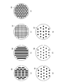
上記マスキングのマスク形状は、GaN結晶層表面が被覆されるものであれば特に制限されるものではなく、図4に示すように、ストライプ状マスク、格子状マスク、ドット状マスク、ハニカム状マスクなど様々な形状が採用される。格子状マスクの格子は、直交して良いし、所定の角度でクロスしてもよい。ドットの形状も特に制限はなく、円形、三角形、正方形、六角形などが具体的に挙げられる。
上記マスクを構成するユニット、例えば、前記ストライプ状マスクの場合は線、ドット状マスクの場合のドットは、相互に等間隔に存在することが好ましい。また、上記ユニットは単一であってもよいし、複数の集合体であってもよい。例えば、ストライプ状マスクを構成する線は1本でもよいし、複数本の線の組み合わせでもよい。
上記マスクを構成するユニット、例えば、前記ストライプ状マスクの場合は線、ドット状マスクの場合のドットは、相互に等間隔に存在することが好ましい。また、上記ユニットは単一であってもよいし、複数の集合体であってもよい。例えば、ストライプ状マスクを構成する線は1本でもよいし、複数本の線の組み合わせでもよい。
目的とするGaNの結晶面方位(使用するサファイア下地基板の面方位)が、{0001}面({0001}面)の場合は、成長面内の面方位内において6回の対称性を持つため、上記の何れのマスクを使用しても、クラックの発生や結晶の割れには、ほとんど影響しない。即ちマスク形状への依存性が少ない。しかしながら、GaNの結晶面方位(使用するサファイア下地基板の面方位)が、{11-22}面({-1012}面)、{10-11}面({11-23}面)、{20-21}面({22-43}面)等の場合は、成長面の面方位内において二本の直交する対称軸を有しており、各軸の熱膨張率の差異が顕著に出てクラックの発生が起こりやすいので、歪を多方向から分散して緩和できるマスクが好ましい。この点から、特に、ドットが円形のドット状マスクが好ましい。
図4(e)、(f)、(g)に、各種形状のドット状のマスクを示す。ドット状マスクにおいて、ドットの直径とは、円形以外は各ドットの外接円の直径をいう。当該直径が0.1~100μmであって、あるドットの中心と隣接するドットの中心との距離は0.2~200μmであり、これらのドットが規則的に配列されたマスクが好適に採用される。ドットの直径が0.1μm未満であると結晶表面の平滑性構造への効果が低減する傾向があり、100μmを超えるとマスク上からの異常成長の可能性が高くなり、多結晶体となる傾向にある。一方、あるドットの中心と隣接するドットの中心との距離が0.2μm未満であると選択横方向成長における欠陥密度低下の効果が低減する傾向がある。200μmを超えた場合も同様に欠陥密度低下の効果が低減する傾向がある。
図4(b)に示すようなストライプ状のマスクにおいて、ストライプのマスク幅(短軸幅)は、通常、0.5~500μmであり、開口幅(ストライプ同士の間隔)は、通常、0.5~50μmである。ストライプのマスク幅が0.5μm未満であると結晶表面の平滑性構造への効果が低減する傾向があり、500μmを超えるとマスク上からの異常成長の可能性が高くなり、多結晶体となる傾向にある。一方、開口幅が0.5μm未満であると選択横方向成長における欠陥密度低下の効果が低減する傾向がある。50μmを超えた場合も同様に欠陥密度低下の効果が低減する傾向がある。
本発明において、前記ストライプ状マスクを使用する場合、溝部の長軸方向とストライプの長軸方向のなす交差角度を大きくさせることは、クラックの発生を防止させることができ、暗点密度低減を低減させることができ、好ましい。
即ち、本発明で使用するサファイア下地基板は単結晶であり、目的とするGaN結晶の結晶方位に対応させた、前述の通りの様々に選択された結晶主面を持つ。それ故、当該基板は、直交する異なる2つの熱膨張係数を有している。したがって、ストライプ状のマスクを熱膨張の大きい方向と平行に形成することにより、GaN結晶層と溝部形成サファイア下地基板間にかかる歪を緩衝することができ、ひいてはHVPE法により形成されるGaN結晶の割れを防止できる。
即ち、本発明で使用するサファイア下地基板は単結晶であり、目的とするGaN結晶の結晶方位に対応させた、前述の通りの様々に選択された結晶主面を持つ。それ故、当該基板は、直交する異なる2つの熱膨張係数を有している。したがって、ストライプ状のマスクを熱膨張の大きい方向と平行に形成することにより、GaN結晶層と溝部形成サファイア下地基板間にかかる歪を緩衝することができ、ひいてはHVPE法により形成されるGaN結晶の割れを防止できる。
MOVPE法により形成した半極性又は無極性のGaN結晶層の表面の一部を、上記の通りのマスキング処理を行った後、更にその上にHVPE法で高速の結晶形成を行う。当該マスキング処理を行うことにより、半極性又は無極性のGaN結晶であっても、クラックの発生が少なく、且つ、表面が平坦な、しかも数mmの膜厚で大面積のGaN結晶が得られる。
HVPE法は、塩化ガリウムと、窒素源となるアンモニア等を、気相反応させて下地基板上にGaN結晶をエピタキシャル成長させる方法であり、それ自体公知の方法である。
結晶成長に用いられるHVPE装置は、大きくは反応管、加熱系、ガス供給系、及びガス排気系から構成される。ガス供給系はマスフローコントローラーによって、ガス供給量の精密な制御が可能である。加熱系は、石英製の反応管を抵抗加熱式のヒーターで覆い、反応管、及びその中に設置される基板やサセプタ、金属原料を加熱するホットウォール法が用いられている。ホットウォール法を用いることにより、原料ガスを充分に加熱して基板表面に供給することができ、供給原料の飽和蒸気圧を高くすることができる。その結果、多量の原料供給が可能となり高速成長を実現できる。
結晶成長に用いられるHVPE装置は、大きくは反応管、加熱系、ガス供給系、及びガス排気系から構成される。ガス供給系はマスフローコントローラーによって、ガス供給量の精密な制御が可能である。加熱系は、石英製の反応管を抵抗加熱式のヒーターで覆い、反応管、及びその中に設置される基板やサセプタ、金属原料を加熱するホットウォール法が用いられている。ホットウォール法を用いることにより、原料ガスを充分に加熱して基板表面に供給することができ、供給原料の飽和蒸気圧を高くすることができる。その結果、多量の原料供給が可能となり高速成長を実現できる。
反応管の中は大きく金属原料部と基板加熱部に分けられる。金属原料部にはGa金属が置かれており、高温下にて、HClガスを供給することにより、Ga金属とHClガスとが反応し、GaClが生成する。生成したGaClガスは、石英製の配管を通り、基板加熱部へと運ばれる。基板加熱部には、ガスの流れに対して垂直に炭素製或いはSiCのサセプタが配置され、サセプタは自転機構を有している。そして、そのサセプタ上にサファイア下地基板、もしくは、サファイア下地基板上にGaN結晶を成長させた積層基板がセットされ、金属原料部で生成したGaClガス、及び、NH3ガスとが基板上で反応することで、GaN結晶の成長が進行する。
結晶成長には原料ガスとして窒素原料であるNH3ガス、Ga源であるGaClを生成するためのHClガスが用いられる。GaCl生成には、HClガスの代わりにCl2ガスを使用しても良い。またGa原料であるGa金属は装置内に設置される。原料ガスであるNH3とHClガスの他に、H2やN2などのキャリアガスが用いられる。
結晶成長には原料ガスとして窒素原料であるNH3ガス、Ga源であるGaClを生成するためのHClガスが用いられる。GaCl生成には、HClガスの代わりにCl2ガスを使用しても良い。またGa原料であるGa金属は装置内に設置される。原料ガスであるNH3とHClガスの他に、H2やN2などのキャリアガスが用いられる。
HVPE法による結晶形成後の結晶成長炉から取り出した時点における、即ちアズグロウンの窒化ガリウム結晶表面のRMSは、300nm未満、好適には30nm未満であって、表面の平滑性に優れるGaN結晶が得られる。
上記HVPE法による厚膜のGaN結晶を育成した後、レーザー照射分離や研磨等の公知の方法により、下地基板を分離してGaNの自立基板が得られる。
しかしながら、レーザー照射分離や研磨等の方法では、GaN結晶へのダメージが発生する恐れがあり、しかも、必ずしも効率的な分離方法ではない。
前記溝部形成サファイア下地基板を用いて膜厚が100μm以上、好適には300μm以上のGaN結晶を成長した後、基板の冷却を行うと、特別に機械的応力を印加することなく、冷却時の熱応力のみにてサファイア下地基板とGaN結晶層との界面において自然剥離が生じて分離できる。冷却は、例えば、低温ガス等を供給して強制的に行ってもよく、また、自然放冷によって行ってもよい。冷却によってサファイア下地基板、及びGaN結晶層の温度を20℃~150℃まで低下させる。冷却速度は、例えば、1~100℃/minである。
しかしながら、レーザー照射分離や研磨等の方法では、GaN結晶へのダメージが発生する恐れがあり、しかも、必ずしも効率的な分離方法ではない。
前記溝部形成サファイア下地基板を用いて膜厚が100μm以上、好適には300μm以上のGaN結晶を成長した後、基板の冷却を行うと、特別に機械的応力を印加することなく、冷却時の熱応力のみにてサファイア下地基板とGaN結晶層との界面において自然剥離が生じて分離できる。冷却は、例えば、低温ガス等を供給して強制的に行ってもよく、また、自然放冷によって行ってもよい。冷却によってサファイア下地基板、及びGaN結晶層の温度を20℃~150℃まで低下させる。冷却速度は、例えば、1~100℃/minである。
以下、本発明を、実施例を挙げて具体的に説明するが、本発明はこれらの実施例によって何ら制限されるものではない。また、実施例の中で説明されている特徴の組み合わせすべてが本発明の解決手段に必須のものとは限らない。
実施例1
〔GaN結晶層の形成〕
{10-12}面サファイア基板上にストライプ状にレジストをパターニングし、次いで反応性イオンエッチング(RIE)によりドライエッチングすることで、サファイア基板上に複数本の溝部を形成した。溝部は溝開口幅が3μm、溝の深さが1μm、及び隣接する溝部までの基板主面部分の幅が3μmとなるように形成した。
ドライエッチングの後、レジストを洗浄除去することで溝部形成サファイア下地基板を得た。この溝部形成サファイア下地基板は、基板主面(2インチφ)、基板主面に複数本形成された溝部の側壁から構成される表面露出した結晶成長領域(C面)、及び溝部底面を有する。
作成した溝部形成サファイア下地基板を、MOVPE装置内に、基板上面が上向きになるように石英トレイをセットした後、基板を1150℃に加熱するとともに反応容器内の圧力を100kPaとし、また、反応容器内にキャリアガスとしてH2を10L/minで流通させ、その状態を10分間保持することにより基板をサーマルクリーニングした。
〔GaN結晶層の形成〕
{10-12}面サファイア基板上にストライプ状にレジストをパターニングし、次いで反応性イオンエッチング(RIE)によりドライエッチングすることで、サファイア基板上に複数本の溝部を形成した。溝部は溝開口幅が3μm、溝の深さが1μm、及び隣接する溝部までの基板主面部分の幅が3μmとなるように形成した。
ドライエッチングの後、レジストを洗浄除去することで溝部形成サファイア下地基板を得た。この溝部形成サファイア下地基板は、基板主面(2インチφ)、基板主面に複数本形成された溝部の側壁から構成される表面露出した結晶成長領域(C面)、及び溝部底面を有する。
作成した溝部形成サファイア下地基板を、MOVPE装置内に、基板上面が上向きになるように石英トレイをセットした後、基板を1150℃に加熱するとともに反応容器内の圧力を100kPaとし、また、反応容器内にキャリアガスとしてH2を10L/minで流通させ、その状態を10分間保持することにより基板をサーマルクリーニングした。
次いで、基板の温度を460℃とすると共に反応容器内の圧力を100kPaとし、また、反応容器内を流通させるキャリアガスH2を5L/minの流量で流しながら、そこにV族元素供給源(NH3)、及びIII族元素供給源(TMG)を、それぞれの供給量が5L/min及び5.5μmol/minで基板上にアモルファス上のGaNを約25nm体積させた。続いて基板の温度を1025℃とすると共に反応容器内の圧力を20kPaとし、また、反応容器内を流通させるキャリアガスをH2として、それを5L/minの流量で流通させることで、基板上に堆積したGaNを再結晶化し、溝部側壁の結晶成長領域に選択的にGaN結晶核を形成した。
続いて、基板の温度を1075℃とすると共に反応容器内の圧力を20kPaとし、また、反応容器内を流通させるキャリアガスをH2として、それを5L/minの流量で流通させながら、そこにV族元素供給源(NH3)、及びIII族元素供給源(TMG)を、それぞれの供給量が2L/min及び30μmol/minとなるように300分間流し、GaNを成長させることにより、基板の主面に複数本形成された溝部の各側壁から成長したGaN結晶同士を会合し、基板主面に対して平行に表面が形成されるように{11-22}面GaN結晶層を形成した。
続いて、基板の温度を1075℃とすると共に反応容器内の圧力を20kPaとし、また、反応容器内を流通させるキャリアガスをH2として、それを5L/minの流量で流通させながら、そこにV族元素供給源(NH3)、及びIII族元素供給源(TMG)を、それぞれの供給量が2L/min及び30μmol/minとなるように300分間流し、GaNを成長させることにより、基板の主面に複数本形成された溝部の各側壁から成長したGaN結晶同士を会合し、基板主面に対して平行に表面が形成されるように{11-22}面GaN結晶層を形成した。
〔ストライプ状マスキング〕
作成したGaN結晶層(成長表面)上にレジストをスピンコートした。次いでフォトリソグラフィー法にてサファイア基板の溝部に対して90°となる向きにストライプ状にレジストのパターニングを行った。次いでスパッタリングによりSiO2を100nm成膜した。成膜の後、レジストを洗浄除去することでGaN結晶層上に複数本のストライプを有するSiO2層を形成した。ストライプ幅は3μm、マスクの高さは100nm、開口幅は3μmであった。
GaN結晶成長表面に対するマスキングの割合、即ち、「成長表面マスク被覆率」、並びに「会合部表面マスク被覆率」は以下の通り定義され、各々次のようにして算出した。
「成長表面マスク被覆率」
=(マスク部分の総面積/GaN結晶表面の面積)×100
「会合部表面マスク被覆率」
=(GaN結晶層表面に存在する会合部のマスキング面積/GaN結晶層表面に存在する結晶会合部の結晶表面における総面積)×100
GaN結晶表面の面積は、下地基板の面積とし、その表面におけるマスク部部の総面積は、ストライプ幅と開口幅の間隔から求められる。「成長表面マスク被覆率」は50%である。
結晶会合部のGaN結晶表面における総面積は、1.01cm2であり、会合部表面のマスキング部の総面積は、0.50cm2となる。従って、「会合部表面マスク被覆率」は50%である。
作成したGaN結晶層(成長表面)上にレジストをスピンコートした。次いでフォトリソグラフィー法にてサファイア基板の溝部に対して90°となる向きにストライプ状にレジストのパターニングを行った。次いでスパッタリングによりSiO2を100nm成膜した。成膜の後、レジストを洗浄除去することでGaN結晶層上に複数本のストライプを有するSiO2層を形成した。ストライプ幅は3μm、マスクの高さは100nm、開口幅は3μmであった。
GaN結晶成長表面に対するマスキングの割合、即ち、「成長表面マスク被覆率」、並びに「会合部表面マスク被覆率」は以下の通り定義され、各々次のようにして算出した。
「成長表面マスク被覆率」
=(マスク部分の総面積/GaN結晶表面の面積)×100
「会合部表面マスク被覆率」
=(GaN結晶層表面に存在する会合部のマスキング面積/GaN結晶層表面に存在する結晶会合部の結晶表面における総面積)×100
GaN結晶表面の面積は、下地基板の面積とし、その表面におけるマスク部部の総面積は、ストライプ幅と開口幅の間隔から求められる。「成長表面マスク被覆率」は50%である。
結晶会合部のGaN結晶表面における総面積は、1.01cm2であり、会合部表面のマスキング部の総面積は、0.50cm2となる。従って、「会合部表面マスク被覆率」は50%である。
〔GaN厚膜の形成〕
作成したマスク付きGaN結晶を、HVPE装置内にマスクがガスの上流を向くように炭素製資料固定台にセットした後、反応管内にN2ガスを30min流通させ、反応管内をN2ガス雰囲気下とした。金属原料部が850℃、基板加熱部が1100℃となるように反応管を加熱し、設定温度到達後、25分間保持した。このとき、基板加熱部が500℃に達するまでは反応管内にはN2ガスを流通させ、500℃以上ではH2ガス、及び、NH3ガスを流通させた。
次いで、反応管内に設置されたGa金属にHClガスを1.2L/min流通させた。また、NH3ガスを36L/min、キャリアガスであるH2ガスを4.1L/min流通し、240分間GaN結晶を成長させた。GaN結晶の膜厚は2500μmであった。
その後、HClガスの流通を止めて、成長を終了させ、基板の冷却を行った。冷却はガスを流通させながら、自然放冷にて行った。冷却時、基板温度が600℃以下になるまではNH3ガスを5L/mind流通し、600℃以下ではN2ガスを37.7L/min流通した。
基板温度が150℃以下になった時点で、装置内から基板を取り出したところ、その時点においてすでにサファイア下地基板とGaN結晶層とは50%以上の面積で剥離しており、剥離していない部分についてもSUS製のピンセットで容易に剥離できた。
作成したマスク付きGaN結晶を、HVPE装置内にマスクがガスの上流を向くように炭素製資料固定台にセットした後、反応管内にN2ガスを30min流通させ、反応管内をN2ガス雰囲気下とした。金属原料部が850℃、基板加熱部が1100℃となるように反応管を加熱し、設定温度到達後、25分間保持した。このとき、基板加熱部が500℃に達するまでは反応管内にはN2ガスを流通させ、500℃以上ではH2ガス、及び、NH3ガスを流通させた。
次いで、反応管内に設置されたGa金属にHClガスを1.2L/min流通させた。また、NH3ガスを36L/min、キャリアガスであるH2ガスを4.1L/min流通し、240分間GaN結晶を成長させた。GaN結晶の膜厚は2500μmであった。
その後、HClガスの流通を止めて、成長を終了させ、基板の冷却を行った。冷却はガスを流通させながら、自然放冷にて行った。冷却時、基板温度が600℃以下になるまではNH3ガスを5L/mind流通し、600℃以下ではN2ガスを37.7L/min流通した。
基板温度が150℃以下になった時点で、装置内から基板を取り出したところ、その時点においてすでにサファイア下地基板とGaN結晶層とは50%以上の面積で剥離しており、剥離していない部分についてもSUS製のピンセットで容易に剥離できた。
得られたGaN結晶自立基板の特性を、以下の方法で測定した。
〔暗点密度評価〕
得られたGaN結晶自立基板について、走査型電子顕微鏡/カソードルミネッセンス(SEM/CL)装置(日本電子社製JSM―7600F/Gatan社製MonoCL4)を用いて、GaN結晶自立基板の表面の観察を行った。このときの加速電圧は5kV、観察範囲は20μm×20μmとし、観察範囲内に観察された暗点の総数から暗点密度を算出した。
〔クラック本数評価〕
得られたGaN結晶自立基板について、高強度ハロゲン光を照射し、結晶内に存在するクラックの本数を測定した。
〔表面凹凸〕
得られたGaN結晶自立基板について、ノギスを用いて結晶の全表面の最大高低差を評価し、200μm以上の高低差のものを表面凹凸有、200μm未満の高低差のものを表面凹凸無とし判別した。
〔RMS〕
得られたGaN結晶自立基板について、表面の観察を行った。このときの観察視野範囲は140μm×105μmとし、観察視野範囲内の表面粗さ(RMS)を算出した。
〔暗点密度評価〕
得られたGaN結晶自立基板について、走査型電子顕微鏡/カソードルミネッセンス(SEM/CL)装置(日本電子社製JSM―7600F/Gatan社製MonoCL4)を用いて、GaN結晶自立基板の表面の観察を行った。このときの加速電圧は5kV、観察範囲は20μm×20μmとし、観察範囲内に観察された暗点の総数から暗点密度を算出した。
〔クラック本数評価〕
得られたGaN結晶自立基板について、高強度ハロゲン光を照射し、結晶内に存在するクラックの本数を測定した。
〔表面凹凸〕
得られたGaN結晶自立基板について、ノギスを用いて結晶の全表面の最大高低差を評価し、200μm以上の高低差のものを表面凹凸有、200μm未満の高低差のものを表面凹凸無とし判別した。
〔RMS〕
得られたGaN結晶自立基板について、表面の観察を行った。このときの観察視野範囲は140μm×105μmとし、観察視野範囲内の表面粗さ(RMS)を算出した。
得られた結晶は、{11-22}面を主面とする、厚みが2500μmで、RMSが300nm未満の自立GaN基板であった。表側にはクラックは確認できなかった。裏側には下地基板のサファイアが一部付着していたが、割れることなく自発分離して、GaN結晶のみからなっていた。暗点密度は4.09×10⁵個/cm2であった。
実施例2
GaN結晶層は実施例1と同様にして形成した。続いて、GaN結晶成長表面上に平面視において1辺5μmの正三角形の各頂点に直径3μmの円が配列された高さ100nmのSiO2からなるドット状マスクを形成した。次いで、GaN厚膜を実施例1と同様にして形成して、{11-22}面を主面とする、同等の面積を有する、厚みが2500μmで、RMSが300nm未満の自立GaN基板を得た。表側には、1本のクラックが入っていた。裏側には下地基板のサファイアが一部付着していたが、自発分離してGaN結晶のみからなっていた。暗点密度は9.02×10⁵個/cm2であった。
GaN結晶層は実施例1と同様にして形成した。続いて、GaN結晶成長表面上に平面視において1辺5μmの正三角形の各頂点に直径3μmの円が配列された高さ100nmのSiO2からなるドット状マスクを形成した。次いで、GaN厚膜を実施例1と同様にして形成して、{11-22}面を主面とする、同等の面積を有する、厚みが2500μmで、RMSが300nm未満の自立GaN基板を得た。表側には、1本のクラックが入っていた。裏側には下地基板のサファイアが一部付着していたが、自発分離してGaN結晶のみからなっていた。暗点密度は9.02×10⁵個/cm2であった。
実施例3
GaN結晶層は実施例1と同様にして形成した。続いて、サファイア基板上の溝部に対して平行をなす角度でSiO2からなるストライプ状マスクを形成した。ストライプ幅、開口幅、マスク高さは実施例1と同じであった。次いで、GaN厚膜の形成を実施例1と同様にして行い、{11-22}面を主面とする、厚みが2500μmで、RMSが300nm未満の自立GaN基板を得た。表側にはクラックは確認できなかった。裏側には下地基板のサファイアが一部付着していたが、割れることなく自発分離して、GaN結晶のみからなっていた。暗点密度は2.14×10⁶個/cm2であった。
GaN結晶層は実施例1と同様にして形成した。続いて、サファイア基板上の溝部に対して平行をなす角度でSiO2からなるストライプ状マスクを形成した。ストライプ幅、開口幅、マスク高さは実施例1と同じであった。次いで、GaN厚膜の形成を実施例1と同様にして行い、{11-22}面を主面とする、厚みが2500μmで、RMSが300nm未満の自立GaN基板を得た。表側にはクラックは確認できなかった。裏側には下地基板のサファイアが一部付着していたが、割れることなく自発分離して、GaN結晶のみからなっていた。暗点密度は2.14×10⁶個/cm2であった。
実施例4
GaN結晶層は実施例1と同様にして形成した。続いて、サファイア基板上の溝部に対して1°をなす交差角度でSiO2からなるストライプ状マスクを形成した。ストライプ幅、開口幅、マスク高さは実施例1と同じであった。次いで、GaN厚膜の形成を実施例1と同様にして行い、{11-22}面を主面とする、厚みが2500μmで、RMSが300nm未満の自立GaN基板を得た。表側にはクラックは確認できなかった。裏側には下地基板のサファイアが一部付着していたが、割れることなく自発分離して、GaN結晶のみからなっていた。暗点密度は1.93×10⁶個/cm2であった。
GaN結晶層は実施例1と同様にして形成した。続いて、サファイア基板上の溝部に対して1°をなす交差角度でSiO2からなるストライプ状マスクを形成した。ストライプ幅、開口幅、マスク高さは実施例1と同じであった。次いで、GaN厚膜の形成を実施例1と同様にして行い、{11-22}面を主面とする、厚みが2500μmで、RMSが300nm未満の自立GaN基板を得た。表側にはクラックは確認できなかった。裏側には下地基板のサファイアが一部付着していたが、割れることなく自発分離して、GaN結晶のみからなっていた。暗点密度は1.93×10⁶個/cm2であった。
実施例5
GaN結晶層は実施例1と同様にして形成した。続いて、サファイア基板上の溝部に対して30°をなす交差角度でSiO2からなるストライプ状マスクを形成した。ストライプ幅、開口幅、マスク高さは実施例1と同じであった。次いで、GaN厚膜の形成を実施例1と同様にして行い、{11-22}面を主面とする、厚みが2500μmで、RMSが300nm未満の自立GaN基板を得た。表側には、1本のクラックが入っていた。裏側には下地基板のサファイアが一部付着していたが、自発分離してGaN結晶のみからなっていた。暗点密度は4.60×10⁵個/cm2であった。
GaN結晶層は実施例1と同様にして形成した。続いて、サファイア基板上の溝部に対して30°をなす交差角度でSiO2からなるストライプ状マスクを形成した。ストライプ幅、開口幅、マスク高さは実施例1と同じであった。次いで、GaN厚膜の形成を実施例1と同様にして行い、{11-22}面を主面とする、厚みが2500μmで、RMSが300nm未満の自立GaN基板を得た。表側には、1本のクラックが入っていた。裏側には下地基板のサファイアが一部付着していたが、自発分離してGaN結晶のみからなっていた。暗点密度は4.60×10⁵個/cm2であった。
実施例6
GaN結晶層は実施例1と同様にして形成した。続いて、サファイア基板上の溝部に対して45°をなす交差角度でSiO2からなるストライプ状マスクを形成した。ストライプ幅、開口幅、マスク高さは実施例1と同じであった。次いで、GaN厚膜の形成を実施例1と同様にして行い、{11-22}面を主面とする、厚みが2500μmで、RMSが300nm未満の自立GaN基板を得た。表側にはクラックは確認できなかった。裏側には下地基板のサファイアが一部付着していたが、割れることなく自発分離して、GaN結晶のみからなっていた。暗点密度は6.17×10⁵個/cm2であった。
GaN結晶層は実施例1と同様にして形成した。続いて、サファイア基板上の溝部に対して45°をなす交差角度でSiO2からなるストライプ状マスクを形成した。ストライプ幅、開口幅、マスク高さは実施例1と同じであった。次いで、GaN厚膜の形成を実施例1と同様にして行い、{11-22}面を主面とする、厚みが2500μmで、RMSが300nm未満の自立GaN基板を得た。表側にはクラックは確認できなかった。裏側には下地基板のサファイアが一部付着していたが、割れることなく自発分離して、GaN結晶のみからなっていた。暗点密度は6.17×10⁵個/cm2であった。
実施例7
GaN結晶層は実施例1と同様にして形成した。続いて、サファイア基板上の溝部に対して60°をなす交差角度でSiO2からなるストライプ状マスクを形成した。ストライプ幅、開口幅、マスク高さは実施例1と同じであった。次いで、GaN厚膜の形成を実施例1と同様にして行い、{11-22}面を主面とする、厚みが2500μmで、RMSが300nm未満の自立GaN基板を得た。表側には、1本のクラックが入っていた。裏側には下地基板のサファイアが一部付着していたが、自発分離してGaN結晶のみからなっていた。暗点密度は7.77×10⁵個/cm2であった。
GaN結晶層は実施例1と同様にして形成した。続いて、サファイア基板上の溝部に対して60°をなす交差角度でSiO2からなるストライプ状マスクを形成した。ストライプ幅、開口幅、マスク高さは実施例1と同じであった。次いで、GaN厚膜の形成を実施例1と同様にして行い、{11-22}面を主面とする、厚みが2500μmで、RMSが300nm未満の自立GaN基板を得た。表側には、1本のクラックが入っていた。裏側には下地基板のサファイアが一部付着していたが、自発分離してGaN結晶のみからなっていた。暗点密度は7.77×10⁵個/cm2であった。
実施例8
GaN結晶層は実施例1と同様にして形成した。続いて、サファイア基板上の溝部に対して89°をなす交差角度でSiO2からなるストライプ状マスクを形成した。ストライプ幅、開口幅、マスク高さは実施例1と同じであった。次いで、GaN厚膜の形成を実施例1と同様にして行い、{11-22}面を主面とする、厚みが2500μm、RMSが300nm未満の自立GaN基板を得た。表側にはクラックは確認できなかった。裏側には下地基板のサファイアが一部付着していたが、割れることなく自発分離して、GaN結晶のみからなっていた。暗点密度は4.24×10⁵個/cm2であった。
GaN結晶層は実施例1と同様にして形成した。続いて、サファイア基板上の溝部に対して89°をなす交差角度でSiO2からなるストライプ状マスクを形成した。ストライプ幅、開口幅、マスク高さは実施例1と同じであった。次いで、GaN厚膜の形成を実施例1と同様にして行い、{11-22}面を主面とする、厚みが2500μm、RMSが300nm未満の自立GaN基板を得た。表側にはクラックは確認できなかった。裏側には下地基板のサファイアが一部付着していたが、割れることなく自発分離して、GaN結晶のみからなっていた。暗点密度は4.24×10⁵個/cm2であった。
実施例9
〔GaN結晶層の形成〕
{11-23}面サファイア基板上にスパッタリングによりSiO2を成膜した。次いでストライプ状にレジストをパターニングし、次いで反応性イオンエッチング(RIE)によりドライエッチングすることで、サファイア基板上に複数本の溝部を形成した。溝部は溝開口幅が2μm、溝の深さが1μm、及び隣接する溝部までの基板主面部分の幅が2μmとなるように形成すると共に、基板主面部分をSiO2からなる結晶成長阻害層で被覆した下地基板を作製した。
ドライエッチングの後、レジストを洗浄除去することで溝部形成サファイア下地基板を得た。この溝部形成サファイア下地基板は、基板主面、複数本形成された溝部の側壁から構成される表面露出した結晶成長領域、及び溝部底面を有する。
作成した溝部形成サファイア下地基板を、MOVPE装置内に、基板上面が上向きになるように石英トレイをセットした後、基板を1150℃に加熱するとともに反応容器内の圧力を100kPaとし、また、反応容器内にキャリアガスとしてH2を10L/minで流通させ、その状態を10分間保持することにより基板をサーマルクリーニングした。
〔GaN結晶層の形成〕
{11-23}面サファイア基板上にスパッタリングによりSiO2を成膜した。次いでストライプ状にレジストをパターニングし、次いで反応性イオンエッチング(RIE)によりドライエッチングすることで、サファイア基板上に複数本の溝部を形成した。溝部は溝開口幅が2μm、溝の深さが1μm、及び隣接する溝部までの基板主面部分の幅が2μmとなるように形成すると共に、基板主面部分をSiO2からなる結晶成長阻害層で被覆した下地基板を作製した。
ドライエッチングの後、レジストを洗浄除去することで溝部形成サファイア下地基板を得た。この溝部形成サファイア下地基板は、基板主面、複数本形成された溝部の側壁から構成される表面露出した結晶成長領域、及び溝部底面を有する。
作成した溝部形成サファイア下地基板を、MOVPE装置内に、基板上面が上向きになるように石英トレイをセットした後、基板を1150℃に加熱するとともに反応容器内の圧力を100kPaとし、また、反応容器内にキャリアガスとしてH2を10L/minで流通させ、その状態を10分間保持することにより基板をサーマルクリーニングした。
次いで、基板の温度を460℃とすると共に反応容器内の圧力を100kPaとし、また、反応容器内を流通させるキャリアガスをH2を5L/minの流量で流しながら、そこにV族元素供給源(NH3)、及びIII族元素供給源(TMG)を、それぞれの供給量が5L/min及び5.5μmol/minで基板上にアモルファス上のGaNを約25nm体積させた。続いて基板の温度を1050℃とすると共に反応容器内の圧力を20kPaとし、また、反応容器内を流通させるキャリアガスをH2として、それを5L/minの流量で流通させることで、基板上に堆積したGaNを再結晶化し、溝部側壁の結晶成長領域に選択的にGaN結晶核を形成した。
続いて、基板の温度を1050℃とすると共に反応容器内の圧力を20kPaとし、また、反応容器内を流通させるキャリアガスをH2として、それを5L/minの流量で流通させながら、そこにV族元素供給源(NH3)、及びIII族元素供給源(TMG)を、それぞれの供給量が2L/min及び30μmol/minとなるように180分間流し、GaNを成長させることにより、基板の主面に複数本形成された溝部の各側壁から成長したGaN結晶同士を会合し、基板主面に対して平行に表面が形成されるように{10-11}面GaN結晶層を形成した。
続いて、基板の温度を1050℃とすると共に反応容器内の圧力を20kPaとし、また、反応容器内を流通させるキャリアガスをH2として、それを5L/minの流量で流通させながら、そこにV族元素供給源(NH3)、及びIII族元素供給源(TMG)を、それぞれの供給量が2L/min及び30μmol/minとなるように180分間流し、GaNを成長させることにより、基板の主面に複数本形成された溝部の各側壁から成長したGaN結晶同士を会合し、基板主面に対して平行に表面が形成されるように{10-11}面GaN結晶層を形成した。
〔マスキングとGaN厚膜の形成〕
次いで、このGaN結晶成長表面上へのマスキング及びGaN厚膜の形成を実施例1と同様にして行いった。「成長表面マスク被覆率」は50%であり、「会合部表面マスク被覆率」は50%であった。
{10-11}面を主面とする、下地基板と同等の面積を有する、厚みが2000μmで、RMSが11.1nmの自立GaN基板を得た。表側には、1本のクラックが入っていた。裏側には下地基板のサファイアが一部付着していたが、自発分離してGaN結晶のみからなっていた。暗点密度は3.61×10⁷個/cm2であった。
次いで、このGaN結晶成長表面上へのマスキング及びGaN厚膜の形成を実施例1と同様にして行いった。「成長表面マスク被覆率」は50%であり、「会合部表面マスク被覆率」は50%であった。
{10-11}面を主面とする、下地基板と同等の面積を有する、厚みが2000μmで、RMSが11.1nmの自立GaN基板を得た。表側には、1本のクラックが入っていた。裏側には下地基板のサファイアが一部付着していたが、自発分離してGaN結晶のみからなっていた。暗点密度は3.61×10⁷個/cm2であった。
実施例10
GaN結晶層は実施例9と同様にして形成した。続いて、マスクの形成を実施例2と同様にして行った。次いで、GaN厚膜の形成を実施例9と同様にして行い、{10-11}面を主面とする、厚みが2000μmで、RMSが16.1nmの自立GaN基板を得た。表側には、1本のクラックが入っていた。裏側には下地基板のサファイアが一部付着していたが、自発分離してGaN結晶のみからなっていた。暗点密度は3.90×10⁷個/cm2であった。
GaN結晶層は実施例9と同様にして形成した。続いて、マスクの形成を実施例2と同様にして行った。次いで、GaN厚膜の形成を実施例9と同様にして行い、{10-11}面を主面とする、厚みが2000μmで、RMSが16.1nmの自立GaN基板を得た。表側には、1本のクラックが入っていた。裏側には下地基板のサファイアが一部付着していたが、自発分離してGaN結晶のみからなっていた。暗点密度は3.90×10⁷個/cm2であった。
実施例11
〔GaN結晶層の形成〕
{22-43}面サファイア基板上にスパッタリングによりSiO2を成膜した。次いでストライプ状にレジストをパターニングし、次いで反応性イオンエッチング(RIE)によりドライエッチングすることで、サファイア基板上に複数本の溝部を形成した。溝部は溝開口幅が3μm、溝の深さが1μm、及び隣接する溝部までの基板主面部分の幅が3μmとなるように形成すると共に、基板主面部分をSiO2からなる結晶成長阻害層で被覆した下地基板を作製した。
ドライエッチングの後、レジストを洗浄除去することでサファイア下地基板を得た。このサファイア下地基板は、基板主面、複数本形成された溝部の側壁から構成される表面露出した結晶成長領域、及び溝部底面を有する。
作成したサファイア下地基板を、MOVPE装置内に、基板上面が上向きになるように石英トレイをセットした後、基板を1150℃に加熱するとともに反応容器内の圧力を100kPaとし、また、反応容器内にキャリアガスとしてH2を10L/minで流通させ、その状態を10分間保持することにより基板をサーマルクリーニングした。
〔GaN結晶層の形成〕
{22-43}面サファイア基板上にスパッタリングによりSiO2を成膜した。次いでストライプ状にレジストをパターニングし、次いで反応性イオンエッチング(RIE)によりドライエッチングすることで、サファイア基板上に複数本の溝部を形成した。溝部は溝開口幅が3μm、溝の深さが1μm、及び隣接する溝部までの基板主面部分の幅が3μmとなるように形成すると共に、基板主面部分をSiO2からなる結晶成長阻害層で被覆した下地基板を作製した。
ドライエッチングの後、レジストを洗浄除去することでサファイア下地基板を得た。このサファイア下地基板は、基板主面、複数本形成された溝部の側壁から構成される表面露出した結晶成長領域、及び溝部底面を有する。
作成したサファイア下地基板を、MOVPE装置内に、基板上面が上向きになるように石英トレイをセットした後、基板を1150℃に加熱するとともに反応容器内の圧力を100kPaとし、また、反応容器内にキャリアガスとしてH2を10L/minで流通させ、その状態を10分間保持することにより基板をサーマルクリーニングした。
次いで、基板の温度を460℃とすると共に反応容器内の圧力を100kPaとし、また、反応容器内を流通させるキャリアガスH2を5L/minの流量で流しながら、そこにV族元素供給源(NH3)、及びIII族元素供給源(TMG)を、それぞれの供給量が5L/min及び5.5μmol/minで基板上にアモルファス上のGaNを約25nm体積させた。続いて基板の温度を1000℃とすると共に反応容器内の圧力を100kPaとし、また、反応容器内を流通させるキャリアガスをH2として、それを5L/minの流量で流通させることで、基板上に堆積したGaNを再結晶化し、溝部側壁の結晶成長領域に選択的にGaN結晶核を形成した。
続いて、基板の温度を1000℃とすると共に反応容器内の圧力を100kPaとし、また、反応容器内を流通させるキャリアガスをH2として、それを5L/minの流量で流通させながら、そこにV族元素供給源(NH3)、及びIII族元素供給源(TMG)を、それぞれの供給量が2L/min及び30μmol/minとなるように300分間流し、GaNを成長させることにより、基板の主面に複数本形成された溝部の各側壁から成長したGaN結晶同士を会合し、基板主面に対して平行に表面が形成されるように{20-21}面GaN結晶層を形成した。
続いて、基板の温度を1000℃とすると共に反応容器内の圧力を100kPaとし、また、反応容器内を流通させるキャリアガスをH2として、それを5L/minの流量で流通させながら、そこにV族元素供給源(NH3)、及びIII族元素供給源(TMG)を、それぞれの供給量が2L/min及び30μmol/minとなるように300分間流し、GaNを成長させることにより、基板の主面に複数本形成された溝部の各側壁から成長したGaN結晶同士を会合し、基板主面に対して平行に表面が形成されるように{20-21}面GaN結晶層を形成した。
〔マスキングとGaN厚膜の形成〕
次いで、このGaN結晶成長表面上へのマスキング及びGaN厚膜の形成を実施例1と同様に行った。「成長表面マスク被覆率」は50%であり、「会合部表面マスク被覆率」は50%であった。
{20-21}面を主面とする、下地基板と同等の面積で、厚みが2200μmで、RMSが280nmの自立GaN基板を得た。表側にはクラックは確認できなかった。裏側には下地基板のサファイアが一部付着していたが、割れることなく自発分離して、GaN結晶のみからなっていた。暗点密度は6.45×10⁷個/cm2であった。
次いで、このGaN結晶成長表面上へのマスキング及びGaN厚膜の形成を実施例1と同様に行った。「成長表面マスク被覆率」は50%であり、「会合部表面マスク被覆率」は50%であった。
{20-21}面を主面とする、下地基板と同等の面積で、厚みが2200μmで、RMSが280nmの自立GaN基板を得た。表側にはクラックは確認できなかった。裏側には下地基板のサファイアが一部付着していたが、割れることなく自発分離して、GaN結晶のみからなっていた。暗点密度は6.45×10⁷個/cm2であった。
実施例12
GaN結晶層は実施例11と同様にして形成した。続いて、実施例2と同様にしてドット状のマスクを形成した。次いで、GaN厚膜の形成を実施例1と同様にして行い、{20-21}面を主面とする、厚みが2200μm、RMSが237.8nmの自立GaN基板を得た。表側にはクラックは確認できなかった。裏側には下地基板のサファイアが一部付着していたが、自発分離してGaN結晶のみからなっていた。暗点密度は7.55×10⁷個/cm2であった。
GaN結晶層は実施例11と同様にして形成した。続いて、実施例2と同様にしてドット状のマスクを形成した。次いで、GaN厚膜の形成を実施例1と同様にして行い、{20-21}面を主面とする、厚みが2200μm、RMSが237.8nmの自立GaN基板を得た。表側にはクラックは確認できなかった。裏側には下地基板のサファイアが一部付着していたが、自発分離してGaN結晶のみからなっていた。暗点密度は7.55×10⁷個/cm2であった。
実施例13
GaN結晶層は実施例11と同様にして形成した。続いて、サファイア基板上の溝部に対して平行及び垂直をなす角度でSiO2からなる格子状マスクを形成した。ストライプ幅、開口幅、マスク高さは実施例3と同じであった。次いで、GaN厚膜の形成を実施例1と同様にして行い、{20-21}面を主面とする、厚みが2200μm、RMSが257.2nmの自立GaN基板を得た。表側にはクラックは確認できなかった。裏側には下地基板のサファイアが一部付着していたが、自発分離してGaN結晶のみからなっていた。暗点密度は7.09×10⁷個/cm2であった。
GaN結晶層は実施例11と同様にして形成した。続いて、サファイア基板上の溝部に対して平行及び垂直をなす角度でSiO2からなる格子状マスクを形成した。ストライプ幅、開口幅、マスク高さは実施例3と同じであった。次いで、GaN厚膜の形成を実施例1と同様にして行い、{20-21}面を主面とする、厚みが2200μm、RMSが257.2nmの自立GaN基板を得た。表側にはクラックは確認できなかった。裏側には下地基板のサファイアが一部付着していたが、自発分離してGaN結晶のみからなっていた。暗点密度は7.09×10⁷個/cm2であった。
比較例1
GaN結晶層は実施例1と同様にして形成した。次いで、マスク形成無しにGaN厚膜の形成を実施例1と同様にして行い、{11-22}面を主面とする、厚み2500μmの自立GaN基板を得た。表面は1500μmを超える凹凸があった。表側には25本のクラックが入っていた。暗点密度は1.18×10⁸個/cm2であった。
GaN結晶層は実施例1と同様にして形成した。次いで、マスク形成無しにGaN厚膜の形成を実施例1と同様にして行い、{11-22}面を主面とする、厚み2500μmの自立GaN基板を得た。表面は1500μmを超える凹凸があった。表側には25本のクラックが入っていた。暗点密度は1.18×10⁸個/cm2であった。

実施例1および比較例1のクラック本数から、マスキングによってクラックが大きく低減する効果が認められる。また、実施例1~13および比較例1の表面凹凸の有無から、マスクによって200μm以上の高低差を有する凹凸が大きく低減される効果が認められる。さらに、実施例1~13のRMSから、マスキングによって表面平坦性が向上していることが分かる。
特に{10-11}面GaN結晶(実施例10)では、HVPE法による結晶形成後の結晶成長炉から取り出した時点における窒化ガリウム結晶表面平坦性が、MOVPE法によるものと同等以上の表面平坦性を有する高品質のGaN結晶自立基板が得られることが認識できる。
特に{10-11}面GaN結晶(実施例10)では、HVPE法による結晶形成後の結晶成長炉から取り出した時点における窒化ガリウム結晶表面平坦性が、MOVPE法によるものと同等以上の表面平坦性を有する高品質のGaN結晶自立基板が得られることが認識できる。
10 溝部形成サファイア下地基板
11 下地基板主面
20 下地基板溝部
21 溝部側壁
22 溝部底面
23 側壁結晶成長領域
30 GaN結晶層
31 GaN結晶層表面
40 溝部側壁マスク部
50 マスク
11 下地基板主面
20 下地基板溝部
21 溝部側壁
22 溝部底面
23 側壁結晶成長領域
30 GaN結晶層
31 GaN結晶層表面
40 溝部側壁マスク部
50 マスク
Claims (11)
- 下地基板の主面に対して傾斜した側壁を有する複数本の溝部を形成したサファイア下地基板上に半極性又は無極性の主面を持つ窒化ガリウム結晶層を成長させて、半極性又は無極性の主面を持つ窒化ガリウム結晶自立基板を製造する方法において、
前記サファイア下地基板上に有機金属気相成長(Metal Organic Vapor Phase Epitaxy:MOVPE)法により、0.05~5μm厚の半極性又は無極性の主面を持つ窒化ガリウム結晶層を形成し、次いで当該結晶層の表面の一部をマスキングした後、当該結晶層表面上にハイドライド気相成長(Hydride Vapor Phase Epitaxy:HVPE)法により0.2~5mm厚の半極性又は無極性の主面を持つ窒化ガリウム結晶層を形成し、その後サファイア下地基板を分離せしめることを特徴とする窒化ガリウム結晶自立基板の製造方法。 - 形成した窒化ガリウム結晶層が、サファイア下地基板の溝部からの結晶成長により形成される複数本の結晶会合部を有し、マスキングが、上記窒化ガリウム結晶層表面に存在する結晶会合部の一部をマスキングすることを特徴とする請求項1に記載の窒化ガリウム結晶自立基板の製造方法。
- マスキングにより、MOVPEによって形成した窒化ガリウム結晶層の成長表面の10~90%が覆われ、且つ、窒化ガリウム結晶層表面に存在する結晶会合部の20%~80%が覆われていることを特徴とする請求項2に記載の窒化ガリウム結晶自立基板の製造方法。
- マスキングに使用するマスクが、ストライプ状の形状を有することを特徴とする請求項1~3の何れか一項に記載の窒化ガリウム結晶自立基板の製造方法。
- マスキングに使用するマスクが、格子状の形状を有することを特徴とする請求項1~3の何れか一項に記載の窒化ガリウム結晶自立基板の製造方法。
- マスキングに使用するマスクが、ドット状の形状を有することを特徴とする請求項1~3の何れか一項に記載の窒化ガリウム結晶自立基板の製造方法。
- 下地基板の窒化ガリウム結晶層を形成する側の全表面積に対して、結晶成長の起点となる側壁の総面積の割合が、1~20%であることを特徴とする請求項1~6に記載の窒化ガリウム結晶自立基板の製造方法。
- 半極性又は無極性の主面を持つ窒化ガリウム結晶自立基板が、{0001}面が<10-10>軸方向に向かって1°~90°傾いた面を主面とする窒化ガリウム結晶自立基板であることを特徴とする請求項1~7の何れか一項に記載の窒化ガリウム結晶自立基板の製造方法。
- 半極性又は無極性の主面を持つ窒化ガリウム結晶自立基板が、{0001}面が<11-20>軸方向に向かって1°~90°傾いた面を主面とする窒化ガリウム結晶自立基板であることを特徴とする請求項1~7の何れか一項に記載の窒化ガリウム結晶自立基板の製造方法。
- 窒化ガリウム結晶自立基板の暗点密度が、2×10⁸個/cm2未満であることを特徴とする請求項1~7の何れか一項に記載の窒化ガリウム結晶自立基板の製造方法。
- HVPE法による結晶形成後の結晶成長炉から取り出した時点における窒化ガリウム結晶表面のRMS(表面粗さ)が、300nm未満であることを特徴とする請求項1~10の何れか一項に記載の窒化ガリウム結晶自立基板の製造方法。
Applications Claiming Priority (2)
| Application Number | Priority Date | Filing Date | Title |
|---|---|---|---|
| JP2013-046913 | 2013-03-08 | ||
| JP2013046913 | 2013-03-08 |
Publications (1)
| Publication Number | Publication Date |
|---|---|
| WO2014136602A1 true WO2014136602A1 (ja) | 2014-09-12 |
Family
ID=51491123
Family Applications (1)
| Application Number | Title | Priority Date | Filing Date |
|---|---|---|---|
| PCT/JP2014/054346 Ceased WO2014136602A1 (ja) | 2013-03-08 | 2014-02-24 | 窒化ガリウム結晶自立基板の製造方法 |
Country Status (2)
| Country | Link |
|---|---|
| JP (1) | JP6346457B2 (ja) |
| WO (1) | WO2014136602A1 (ja) |
Cited By (1)
| Publication number | Priority date | Publication date | Assignee | Title |
|---|---|---|---|---|
| CN110100304A (zh) * | 2016-12-20 | 2019-08-06 | 古河机械金属株式会社 | Iii族氮化物半导体基板及iii族氮化物半导体基板的制造方法 |
Families Citing this family (4)
| Publication number | Priority date | Publication date | Assignee | Title |
|---|---|---|---|---|
| JP6306677B1 (ja) | 2016-12-19 | 2018-04-04 | 古河機械金属株式会社 | Iii族窒化物半導体基板、及び、iii族窒化物半導体基板の製造方法 |
| JP6232150B1 (ja) * | 2017-01-10 | 2017-11-15 | 古河機械金属株式会社 | Iii族窒化物半導体基板、及び、iii族窒化物半導体基板の製造方法 |
| JP7055595B2 (ja) * | 2017-03-29 | 2022-04-18 | 古河機械金属株式会社 | Iii族窒化物半導体基板、及び、iii族窒化物半導体基板の製造方法 |
| US20230115980A1 (en) * | 2021-10-11 | 2023-04-13 | Applied Materials, Inc. | Masking layers in led structures |
Citations (3)
| Publication number | Priority date | Publication date | Assignee | Title |
|---|---|---|---|---|
| JP2005343713A (ja) * | 2004-05-31 | 2005-12-15 | Hitachi Cable Ltd | Iii−v族窒化物系半導体自立基板及びその製造方法並びにiii−v族窒化物系半導体 |
| JP2008037665A (ja) * | 2006-08-02 | 2008-02-21 | Sumitomo Electric Ind Ltd | 窒化ガリウムの結晶成長方法 |
| JP2011042542A (ja) * | 2009-08-24 | 2011-03-03 | Furukawa Co Ltd | Iii族窒化物基板の製造方法およびiii族窒化物基板 |
Family Cites Families (4)
| Publication number | Priority date | Publication date | Assignee | Title |
|---|---|---|---|---|
| JP5023318B2 (ja) * | 2005-05-19 | 2012-09-12 | 国立大学法人三重大学 | 3−5族窒化物半導体積層基板、3−5族窒化物半導体自立基板の製造方法、及び半導体素子 |
| WO2008073414A1 (en) * | 2006-12-12 | 2008-06-19 | The Regents Of The University Of California | Crystal growth of m-plane and semipolar planes of(ai, in, ga, b)n on various substrates |
| DE102010011895B4 (de) * | 2010-03-18 | 2013-07-25 | Freiberger Compound Materials Gmbh | Verfahren zur Herstellung eines semipolaren Gruppe III-Nitrid-Kristalls, Substrat, freistehendes semipolares Substrat und Verwendung der Substrate |
| JP2012184144A (ja) * | 2011-03-07 | 2012-09-27 | Tokuyama Corp | 窒化ガリウム結晶積層基板及びその製造方法 |
-
2014
- 2014-02-24 JP JP2014033208A patent/JP6346457B2/ja not_active Expired - Fee Related
- 2014-02-24 WO PCT/JP2014/054346 patent/WO2014136602A1/ja not_active Ceased
Patent Citations (3)
| Publication number | Priority date | Publication date | Assignee | Title |
|---|---|---|---|---|
| JP2005343713A (ja) * | 2004-05-31 | 2005-12-15 | Hitachi Cable Ltd | Iii−v族窒化物系半導体自立基板及びその製造方法並びにiii−v族窒化物系半導体 |
| JP2008037665A (ja) * | 2006-08-02 | 2008-02-21 | Sumitomo Electric Ind Ltd | 窒化ガリウムの結晶成長方法 |
| JP2011042542A (ja) * | 2009-08-24 | 2011-03-03 | Furukawa Co Ltd | Iii族窒化物基板の製造方法およびiii族窒化物基板 |
Non-Patent Citations (1)
| Title |
|---|
| HIROSHI FURUYA ET AL.: "r-men Sapphire Kako Kibanjo {11-22} GaN Seicho ni Okeru Ten'i Blocking", DAI 59 KAI EXTENDED ABSTRACTS, JAPAN SOCIETY OF APPLIED PHYSICS AND RELATED SOCIETIES, 18 March 2012 (2012-03-18), pages 125 * |
Cited By (5)
| Publication number | Priority date | Publication date | Assignee | Title |
|---|---|---|---|---|
| CN110100304A (zh) * | 2016-12-20 | 2019-08-06 | 古河机械金属株式会社 | Iii族氮化物半导体基板及iii族氮化物半导体基板的制造方法 |
| KR20190097084A (ko) * | 2016-12-20 | 2019-08-20 | 후루카와 기카이 긴조쿠 가부시키가이샤 | Ⅲ족 질화물 반도체 기판 및 ⅲ족 질화물 반도체 기판의 제조방법 |
| EP3561855A4 (en) * | 2016-12-20 | 2020-09-30 | Furukawa Co., Ltd. | GROUP III NITRIDE SEMICONDUCTOR SUBSTRATE AND PROCESS FOR THE PRODUCTION OF GROUP III NITRIDE SEMICONDUCTOR SUBSTRATE |
| KR102415252B1 (ko) | 2016-12-20 | 2022-06-29 | 후루카와 기카이 긴조쿠 가부시키가이샤 | Ⅲ족 질화물 반도체 기판 및 ⅲ족 질화물 반도체 기판의 제조방법 |
| CN110100304B (zh) * | 2016-12-20 | 2023-10-20 | 古河机械金属株式会社 | Iii族氮化物半导体基板及iii族氮化物半导体基板的制造方法 |
Also Published As
| Publication number | Publication date |
|---|---|
| JP6346457B2 (ja) | 2018-06-20 |
| JP2014196230A (ja) | 2014-10-16 |
Similar Documents
| Publication | Publication Date | Title |
|---|---|---|
| JP4932121B2 (ja) | Iii−v族窒化物系半導体基板の製造方法 | |
| JP5276852B2 (ja) | Iii族窒化物半導体エピタキシャル基板の製造方法 | |
| JP5725086B2 (ja) | Iii族窒化物半導体結晶の製造方法、iii族窒化物半導体基板および半導体発光デバイス | |
| JP5392855B2 (ja) | 半導体基板及びその製造方法 | |
| WO2012121154A1 (ja) | 下地基板、窒化ガリウム結晶積層基板及びその製造方法 | |
| JP2011119761A (ja) | Iii−v族窒化物系半導体基板 | |
| US20180158681A1 (en) | Method for manufacturing nitride semiconductor template, nitride semiconductor template and nitride semiconductor device | |
| JP2013173641A (ja) | 窒化ガリウム結晶積層基板及びその製造方法 | |
| JP6346457B2 (ja) | 窒化ガリウム結晶自立基板の製造方法 | |
| JP4907476B2 (ja) | 窒化物半導体単結晶 | |
| JP6404655B2 (ja) | AlNテンプレート基板およびその製造方法 | |
| WO2017134708A1 (ja) | エピタキシャル基板 | |
| JP2017522721A (ja) | 半極性iii族窒化物層を含む半導体材料の製造方法 | |
| JPWO2013058352A1 (ja) | Iii族窒化物半導体結晶 | |
| JP6405767B2 (ja) | 窒化ガリウム基板 | |
| JP5293592B2 (ja) | Iii族窒化物半導体の製造方法およびテンプレート基板 | |
| JP4888377B2 (ja) | 窒化物半導体自立基板 | |
| JP2008037665A (ja) | 窒化ガリウムの結晶成長方法 | |
| JP6044975B2 (ja) | 半導体素子用エピタキシャル基板および半導体素子用エピタキシャル基板の作製方法 | |
| WO2013141099A1 (ja) | 窒化ガリウム結晶自立基板及びその製造方法 | |
| JP5015480B2 (ja) | 半導体単結晶基板の製造方法 | |
| JP2002246322A (ja) | 窒化物半導体基板及びその成長方法 | |
| JP2013209271A (ja) | 周期表第13族金属窒化物半導体基板の製造方法、および、当該製造方法に用いられる下地基板 | |
| JP7084123B2 (ja) | Iii族窒化物半導体基板 | |
| WO2023190969A1 (ja) | GaN結晶及びGaNウエハ |
Legal Events
| Date | Code | Title | Description |
|---|---|---|---|
| 121 | Ep: the epo has been informed by wipo that ep was designated in this application |
Ref document number: 14760719 Country of ref document: EP Kind code of ref document: A1 |
|
| NENP | Non-entry into the national phase |
Ref country code: DE |
|
| 122 | Ep: pct application non-entry in european phase |
Ref document number: 14760719 Country of ref document: EP Kind code of ref document: A1 |