WO2014136359A1 - 有機薄膜太陽電池およびその製造方法、および電子機器 - Google Patents
有機薄膜太陽電池およびその製造方法、および電子機器 Download PDFInfo
- Publication number
- WO2014136359A1 WO2014136359A1 PCT/JP2013/084287 JP2013084287W WO2014136359A1 WO 2014136359 A1 WO2014136359 A1 WO 2014136359A1 JP 2013084287 W JP2013084287 W JP 2013084287W WO 2014136359 A1 WO2014136359 A1 WO 2014136359A1
- Authority
- WO
- WIPO (PCT)
- Prior art keywords
- layer
- solar cell
- electrode layer
- organic thin
- film solar
- Prior art date
- Legal status (The legal status is an assumption and is not a legal conclusion. Google has not performed a legal analysis and makes no representation as to the accuracy of the status listed.)
- Ceased
Links
Images





























Classifications
-
- H—ELECTRICITY
- H10—SEMICONDUCTOR DEVICES; ELECTRIC SOLID-STATE DEVICES NOT OTHERWISE PROVIDED FOR
- H10K—ORGANIC ELECTRIC SOLID-STATE DEVICES
- H10K30/00—Organic devices sensitive to infrared radiation, light, electromagnetic radiation of shorter wavelength or corpuscular radiation
- H10K30/30—Organic devices sensitive to infrared radiation, light, electromagnetic radiation of shorter wavelength or corpuscular radiation comprising bulk heterojunctions, e.g. interpenetrating networks of donor and acceptor material domains
-
- H—ELECTRICITY
- H10—SEMICONDUCTOR DEVICES; ELECTRIC SOLID-STATE DEVICES NOT OTHERWISE PROVIDED FOR
- H10K—ORGANIC ELECTRIC SOLID-STATE DEVICES
- H10K30/00—Organic devices sensitive to infrared radiation, light, electromagnetic radiation of shorter wavelength or corpuscular radiation
- H10K30/80—Constructional details
- H10K30/81—Electrodes
-
- H—ELECTRICITY
- H10—SEMICONDUCTOR DEVICES; ELECTRIC SOLID-STATE DEVICES NOT OTHERWISE PROVIDED FOR
- H10K—ORGANIC ELECTRIC SOLID-STATE DEVICES
- H10K30/00—Organic devices sensitive to infrared radiation, light, electromagnetic radiation of shorter wavelength or corpuscular radiation
- H10K30/80—Constructional details
- H10K30/88—Passivation; Containers; Encapsulations
-
- H—ELECTRICITY
- H10—SEMICONDUCTOR DEVICES; ELECTRIC SOLID-STATE DEVICES NOT OTHERWISE PROVIDED FOR
- H10K—ORGANIC ELECTRIC SOLID-STATE DEVICES
- H10K39/00—Integrated devices, or assemblies of multiple devices, comprising at least one organic radiation-sensitive element covered by group H10K30/00
- H10K39/10—Organic photovoltaic [PV] modules; Arrays of single organic PV cells
-
- H—ELECTRICITY
- H10—SEMICONDUCTOR DEVICES; ELECTRIC SOLID-STATE DEVICES NOT OTHERWISE PROVIDED FOR
- H10K—ORGANIC ELECTRIC SOLID-STATE DEVICES
- H10K77/00—Constructional details of devices covered by this subclass and not covered by groups H10K10/80, H10K30/80, H10K50/80 or H10K59/80
- H10K77/10—Substrates, e.g. flexible substrates
-
- H—ELECTRICITY
- H10—SEMICONDUCTOR DEVICES; ELECTRIC SOLID-STATE DEVICES NOT OTHERWISE PROVIDED FOR
- H10K—ORGANIC ELECTRIC SOLID-STATE DEVICES
- H10K85/00—Organic materials used in the body or electrodes of devices covered by this subclass
- H10K85/10—Organic polymers or oligomers
- H10K85/111—Organic polymers or oligomers comprising aromatic, heteroaromatic, or aryl chains, e.g. polyaniline, polyphenylene or polyphenylene vinylene
- H10K85/113—Heteroaromatic compounds comprising sulfur or selene, e.g. polythiophene
- H10K85/1135—Polyethylene dioxythiophene [PEDOT]; Derivatives thereof
-
- Y—GENERAL TAGGING OF NEW TECHNOLOGICAL DEVELOPMENTS; GENERAL TAGGING OF CROSS-SECTIONAL TECHNOLOGIES SPANNING OVER SEVERAL SECTIONS OF THE IPC; TECHNICAL SUBJECTS COVERED BY FORMER USPC CROSS-REFERENCE ART COLLECTIONS [XRACs] AND DIGESTS
- Y02—TECHNOLOGIES OR APPLICATIONS FOR MITIGATION OR ADAPTATION AGAINST CLIMATE CHANGE
- Y02E—REDUCTION OF GREENHOUSE GAS [GHG] EMISSIONS, RELATED TO ENERGY GENERATION, TRANSMISSION OR DISTRIBUTION
- Y02E10/00—Energy generation through renewable energy sources
- Y02E10/50—Photovoltaic [PV] energy
- Y02E10/549—Organic PV cells
-
- Y—GENERAL TAGGING OF NEW TECHNOLOGICAL DEVELOPMENTS; GENERAL TAGGING OF CROSS-SECTIONAL TECHNOLOGIES SPANNING OVER SEVERAL SECTIONS OF THE IPC; TECHNICAL SUBJECTS COVERED BY FORMER USPC CROSS-REFERENCE ART COLLECTIONS [XRACs] AND DIGESTS
- Y02—TECHNOLOGIES OR APPLICATIONS FOR MITIGATION OR ADAPTATION AGAINST CLIMATE CHANGE
- Y02P—CLIMATE CHANGE MITIGATION TECHNOLOGIES IN THE PRODUCTION OR PROCESSING OF GOODS
- Y02P70/00—Climate change mitigation technologies in the production process for final industrial or consumer products
- Y02P70/50—Manufacturing or production processes characterised by the final manufactured product
Definitions
- the present invention relates to an organic thin-film solar cell, a method for manufacturing the same, and an electronic device, and is particularly inexpensive and has improved durability. Further, the structure for taking out an electrode is improved, and an arbitrary position can be obtained without a large structural change in appearance.
- the present invention relates to an organic thin-film solar cell capable of forming a connection point and capable of being reduced in weight and thickness, a manufacturing method thereof, and an electronic device.
- Organic thin-film solar cells featuring ultra-thin, light weight, and flexibility are manufactured by printing methods such as the ink-jet method at room temperature and atmospheric pressure, realizing a high degree of freedom in shape and excellent design. It is possible (for example, refer to Patent Document 1).
- organic thin-film solar cells by applying a fine pattern to the surface of the organic active layer or electrode, the incident light is effectively confined inside the organic active layer, the current collection effect is enhanced, and the photoelectric conversion efficiency is improved. Yes.
- silver (Ag) or gold (Au) nanoparticle whose particle size is controlled by organic synthesis at the p-type / n-type organic layer interface or the organic layer / electrode interface.
- Particles modified with an alkyl group or a thiol group in order to promote dispersion were used in solution and applied on the respective interfaces by spin coating (see, for example, Patent Document 2).
- Organic thin-film solar cells have had the problem of extremely low photoelectric conversion efficiency compared to other types of solar cells, but digging glass and sheets used in organic EL (Electro-Luminescence) displays It has been found that high durability is obtained when sealing with a desiccant is used.
- organic EL Electro-Luminescence
- an electrode is taken out at the end face of a module composed of cells folded in a strip shape.
- a solar cell is mounted on a mobile terminal or the like that is mainly used indoors, it is difficult to take out an electrode at the end face of the module due to the restrictions on the module shape and area.
- the present inventor has found a structure in which a connection point can be freely formed without causing a large change in appearance by providing a mechanism for taking out electricity generated by the module inside the cell at an arbitrary position. .
- An object of the present invention is to provide an organic thin-film solar cell that is inexpensive, has improved durability, and can be reduced in weight and thickness, and a method for manufacturing the same.
- Another object of the present invention is to provide an organic thin-film solar cell that has a simple structure, reduces manufacturing steps, improves designability, and can be reduced in weight and thickness, a manufacturing method thereof, and an electronic device. is there.
- Another object of the present invention is to provide an organic thin-film solar cell that can improve the electrode lead-out structure, can form a connection point at an arbitrary position without causing a large structural change in appearance, and can be reduced in weight and thickness. It is another object of the present invention to provide a manufacturing method and an electronic device.
- a substrate, a first electrode layer disposed on the substrate, a hole transport layer disposed on the first electrode layer, and the positive electrode A bulk heterojunction organic active layer disposed on the hole transport layer; a second electrode layer disposed on the bulk heterojunction organic active layer; and the substrate facing the first electrode layer, the positive electrode A sealing glass that seals a laminated structure including a hole transport layer, the bulk heterojunction organic active layer, and the second electrode layer; and is disposed between the sealing glass and the substrate;
- An organic thin film solar cell comprising a glass frit for sealing is provided.
- a substrate, a first electrode layer disposed on the substrate, a hole transport layer disposed on the first electrode layer, and a hole transport layer are disposed on the hole transport layer.
- a bulk heterojunction organic active layer, a second electrode layer disposed on the bulk heterojunction organic active layer, a passivation layer disposed on the second electrode layer, and disposed on the passivation layer There is provided an organic thin-film solar cell comprising a colored barrier layer and a backsheet passivation layer disposed on the colored barrier layer.
- a substrate, a first electrode layer disposed on the substrate, a hole transport layer disposed on the first electrode layer, and a hole transport layer are disposed on the hole transport layer.
- a bulk heterojunction organic active layer, a second electrode layer disposed on the bulk heterojunction organic active layer, a passivation layer disposed on the second electrode layer, and a surface facing the substrate A first extraction terminal electrode disposed in a straight direction and penetrating through the passivation layer, the second electrode layer, the bulk heterojunction organic active layer, and the hole transport layer and connected to the first electrode layer
- an organic thin-film solar cell provided with a second lead-out terminal electrode that is disposed in a direction perpendicular to the substrate, penetrates the passivation layer, and is connected to the second electrode layer.
- a substrate, a first electrode layer disposed on the substrate, a hole transport layer disposed on the first electrode layer, and a hole transport layer are disposed on the hole transport layer.
- the first passivation terminal electrode disposed in a direction perpendicular to the substrate, passing through the passivation layer, connected to the VIA electrode layer, passing through the passivation layer, and Second extraction connected to the second electrode layer
- the organic thin film solar cell and a child electrode The organic thin film solar cell and a child electrode.
- an electronic device including the organic thin film solar cell is provided.
- the display device includes an organic thin film solar cell formation region and a character formation region disposed in a peripheral portion of the display region, and the organic thin film solar cell formation region includes a substrate, A first electrode layer disposed on the substrate; a hole transport layer disposed on the first electrode layer; a bulk heterojunction organic active layer disposed on the hole transport layer; and the bulk heterojunction organic A second electrode layer disposed on the active layer; a passivation layer disposed on the second electrode layer; and disposed in a direction perpendicular to the substrate, the passivation layer, the second electrode layer, A bulk heterojunction organic active layer, a first extraction terminal electrode penetrating the hole transport layer and connected to the first electrode layer, and disposed in a direction perpendicular to the substrate; A second lead-out terminal electrode connected to the second electrode layer, the display region and the character forming region including the substrate, and the first electrode disposed on the substrate.
- an electronic device comprising a layer and the passivation layer disposed on the
- the display device includes an organic thin film solar cell formation region and a character formation region disposed in a peripheral portion of the display region, and the organic thin film solar cell formation region includes a substrate, A first electrode layer disposed on the substrate; a hole transport layer disposed on the first electrode layer; a bulk heterojunction organic active layer disposed on the hole transport layer; and the bulk A second electrode layer disposed on the heterojunction organic active layer; and the first electrode layer penetrating through the hole transport layer and the bulk heterojunction organic active layer in a direction perpendicular to the substrate.
- the display area and the character forming area are provided with an electronic device including the substrate, the first electrode layer disposed on the substrate, and the passivation layer disposed on the first electrode layer.
- a step of forming a first electrode on a substrate, a step of forming a hole transport layer on the first electrode layer, and a bulk heterojunction on the hole transport layer A step of forming an organic active layer, a step of forming a second electrode layer on the bulk heterojunction organic active layer, a step of forming a glass frit on a sealing glass, and a resin at a tip portion of the glass frit
- the sealing glass and the substrate are opposed to each other, and the first electrode layer, the hole transport layer, the bulk heterojunction organic active layer, and the second are formed by the glass frit and the resin.
- the display device includes an organic thin film solar cell formation region and a character formation region disposed in a peripheral portion of the display region, and the organic thin film solar cell formation region includes a substrate, A first electrode layer disposed on the substrate; a hole transport layer disposed on the first electrode layer; a bulk heterojunction organic active layer disposed on the hole transport layer; and the bulk heterojunction organic
- a second electrode layer disposed on the active layer, a passivation layer disposed on the second electrode layer, a colored barrier layer disposed on the passivation layer, and disposed on the colored barrier layer.
- a backsheet passivation layer wherein the display area and the character forming area are the substrate, the first electrode layer disposed on the substrate, and the first electrode layer.
- the colored barrier layer corresponding to 1 and the colored barrier layer corresponding to the character forming region are provided with colored electronic devices.
- a step of forming a first electrode on a substrate, a step of forming a hole transport layer on the first electrode layer, and a bulk heterojunction on the hole transport layer A step of forming an organic active layer, a step of forming a second electrode layer on the bulk heterojunction organic active layer, a step of forming a passivation layer on the second electrode layer, and a color on the passivation layer.
- a method for producing an organic thin-film solar cell comprising a step of forming a coloration barrier layer and a step of forming a backsheet passivation layer on the coloration barrier layer.
- a step of forming a first electrode on a substrate, a step of forming a hole transport layer on the first electrode layer, and a bulk heterojunction on the hole transport layer Forming an organic active layer; forming a second electrode layer on the bulk heterojunction organic active layer; forming a passivation layer on the second electrode layer; and facing the substrate Forming a first through-hole penetrating through the passivation layer, the second electrode layer, the bulk heterojunction organic active layer, and the hole transport layer in a straight direction and reaching the first electrode layer; Forming a second through hole penetrating the passivation layer in a direction perpendicular to the substrate and reaching the second electrode layer; and the first electrode layer in the first through hole; Forming connected first extraction terminal electrodes Degree and method of manufacturing the organic thin film solar cell and a step of forming a second take-out terminal electrode connected to the second electrode layer in said second through hole is provided.
- a step of forming a first electrode on a substrate, a step of forming a hole transport layer on the first electrode layer, and a bulk heterojunction on the hole transport layer A step of forming an organic active layer, and a third through hole that penetrates the hole transport layer and the bulk heterojunction organic active layer in a direction perpendicular to the substrate and reaches the first electrode layer Forming a second electrode layer on the bulk heterojunction organic active layer, and forming a VIA electrode layer connected to the first electrode layer through the third through hole; and Forming a passivation layer on the second electrode layer and the VIA electrode layer, and forming a fourth through hole penetrating the passivation layer and reaching the VIA electrode layer in a direction perpendicular to the substrate; And a direction perpendicular to the substrate Forming a second through hole penetrating the passivation layer and reaching the second electrode layer; and forming a first lead terminal electrode connected to the VIA electrode layer in the fourth through hole.
- an organic thin-film solar cell that is inexpensive, has improved durability, and can be reduced in weight and thickness, and a method for manufacturing the same.
- an organic thin-film solar cell that has a simple structure, reduces manufacturing steps, improves designability, and can be reduced in weight and thickness, a manufacturing method thereof, and an electronic device.
- the organic thin-film solar cell which can improve the extraction structure of an electrode, can form a connection point in arbitrary positions, without accompanying a big structural change of an external appearance, and can be reduced in weight and thickness, and its A manufacturing method and an electronic device can be provided.
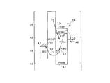
- FIG. 5 is an energy band structure diagram of various materials of the organic thin film solar cell shown in FIG. 4.
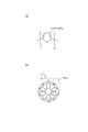
- the chemical structural formula of a material used in vacuum vapor deposition includes (a) Pc: an example of phthalocyanine, (b) ZnPc: an example of zinc phthalocyanine, (c) Example of Me-Ptcdi, (d) Example of C 60 : fullerene.
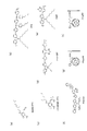
- chemical structural formulas of materials used in a solution process including (a) an example of MDMO-PPV, (b) an example of PFB, (c) CN-MDMO -PPV example, (d) PFO-DBT example, (e) F8BT example, (f) PCDTBT example, (g) PC 60 BM example, (h) PC 70 BM example.
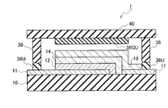
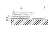
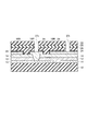
- the typical cross-section figure of the laminated structure part of the organic thin film solar cell which concerns on 1st Embodiment.
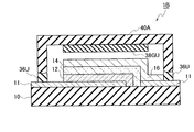
- the typical cross-section figure of the laminated structure part of the organic thin-film solar cell which concerns on the modification of 1st Embodiment.
- FIG. 5 is a process diagram for patterning a second electrode layer on the layer.
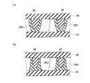
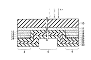
- FIG. 1 is a configuration of a sealing portion of an organic thin-film solar cell according to a first embodiment, and (a) a schematic cross-sectional structure diagram illustrating a configuration in which a glass frit is coated with a UV curable resin, and (b) a glass frit.
- FIG. 3 is a schematic cross-sectional structure diagram showing a configuration of a sealing portion of the organic thin film solar cell according to the first embodiment, in which a porous glass frit is covered with a UV curable resin.
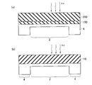
- FIG. 1 is a schematic cross-sectional structure diagram showing a configuration of a sealing portion of an organic thin film solar cell according to a first embodiment, in which (a) two formed glass frits have a wedge shape; Schematic cross-sectional structure diagram showing a configuration in which the glass frit to be formed has a taper shape, (c) a spindle-shaped taper shape in which the cross-sectional shape of the two glass frit formed becomes smaller as the distance from the sealing glass increases The typical cross-section figure which shows the structure which has. 1 is a configuration of a sealing portion of an organic thin film solar cell according to a first embodiment, and (a) a configuration in which two formed glass frit has a wedge shape and is covered with a UV curable resin.
- FIG. 3 is a schematic cross-sectional structure diagram showing a configuration in which the cross-sectional shape has a spindle-shaped taper shape in which the cross-sectional area decreases as the distance from the sealing glass increases, and is covered with a UV curable resin. It is one process of the manufacturing method of the organic thin-film solar cell which concerns on 1st Embodiment, Comprising: (a) Typical plane pattern block diagram which shows the state which formed the transparent electrode layer on the board
- FIG. 1B is a schematic plan pattern configuration diagram showing a state where a hole transport layer is formed on a transparent electrode layer, in one step of the method for manufacturing an organic thin film solar cell according to the first embodiment
- FIG. 20 is a schematic sectional view taken along line 20b-2b in FIG. 1
- FIG. 22B is a schematic sectional view taken along the line 21b-21b in FIG.
- FIG. 22B is a schematic sectional view taken along the line 22b-22b in FIG. It is a process of the manufacturing method of the organic thin-film solar cell concerning 1st Embodiment, Comprising: (a) While etching an excess organic layer by oxygen plasma treatment, an oxide film is formed in the surface of a 2nd electrode layer
- FIG. 24B is a schematic plane pattern configuration diagram showing the state obtained
- FIG. 23B is a schematic cross-sectional structure diagram taken along the line 23b-23b in FIG.
- FIG. 1 is a schematic plan pattern configuration diagram showing a state of a process of manufacturing an organic thin-film solar cell according to a first embodiment, wherein (a) sealing is performed with sealing glass / glass frit and UV curable resin; b) A schematic sectional view taken along the line 24b-24b of FIG.
- FIG. 25 is a schematic cross-sectional structure diagram illustrating a state in which the sealing glass is bent in the structure illustrated in FIG.
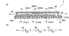
- FIG. 1 is a schematic cross-sectional structure diagram of an organic thin-film solar cell according to a first embodiment, in which an oxygen (O 2 ) gettering sheet is arranged inside a sealing glass and in a space between the sealing glass and the ITO substrate. .
- the typical plane pattern figure which shows the example arrange
- FIG. 30A is a schematic cross-sectional structure diagram taken along line 30a-30a in FIG. 29, and FIG. 30B is an equivalent circuit configuration diagram corresponding to FIG.
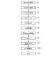
- the flowchart which shows the preparation procedure of the organic thin film solar cell which concerns on 1st Embodiment.
- the typical bird's-eye view structure figure which is one process of the mass production manufacturing process of the organic thin-film solar cell which concerns on 1st Embodiment, and shows the state which formed the stripe pattern of the transparent electrode layer on the board
- 1 is a schematic bird's-eye view showing a state in which a hole transport layer is formed by spin coating on a stripe-shaped transparent electrode layer, which is a step in the mass production process of the organic thin-film solar cell according to the first embodiment. Figure.
- FIG. 1 is a schematic bird's-eye view showing a state in which a bulk heterojunction organic active layer is formed by spin coating on a hole transport layer, which is a step in the mass production manufacturing process of the organic thin-film solar cell according to the first embodiment.
- Structural drawing. 1 is a process of mass production of an organic thin-film solar cell according to a first embodiment, and a stripe pattern of a second electrode layer on a bulk heterojunction organic active layer orthogonal to a striped transparent electrode layer
- the typical bird's-eye view block diagram which shows the state which formed.
- the typical plane pattern block diagram which shows the example which has arrange
- the typical cross-section figure of the laminated structure part of the organic thin-film solar cell which concerns on the modification of 2nd Embodiment. It is one process of the manufacturing method of the organic thin-film solar cell concerning 2nd Embodiment, Comprising: (a) Process drawing which prepares the ITO substrate which formed the transparent electrode layer on the board
- FIG. 5 is a process diagram for patterning a second electrode layer on the layer.
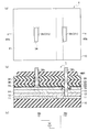
- FIG. 44A is a schematic planar pattern configuration diagram showing a state where a passivation layer is formed on the entire surface of the device, which is a step in the manufacturing process of the organic thin film solar cell according to the second embodiment. ) Is a schematic cross-sectional structure diagram along line 44b-44b.
- FIG. 5B is a schematic plan pattern configuration diagram showing a state in which a colored barrier layer is formed on a passivation layer, which is a step of the manufacturing process of the organic thin-film solar cell according to the second embodiment.
- FIG. 45 is a schematic sectional view taken along line 45b-45b of 45 (a).
- FIG. 6 is a schematic plan pattern configuration diagram showing a state in which a back sheet passivation layer is formed on a colored barrier layer, which is a step of a manufacturing process of an organic thin film solar cell according to a second embodiment;
- FIG. 46 is a schematic sectional view taken along the line 46b-46b of FIG. The typical plane block diagram of the electronic device to which the organic thin-film solar cell which concerns on 2nd Embodiment is applied.
- FIG. 45 is a schematic sectional view taken along line 45b-45b of 45 (a).
- FIG. 6 is a schematic plan pattern configuration diagram showing a state in which a back sheet passivation layer is formed on a colored barrier
- FIG. 48 is a schematic sectional view taken along line 48-48 in FIG.
- FIG. 48 is a schematic sectional view taken along the line 49-49 in FIG.
- FIG. 50 is a schematic sectional view taken along line 50-50 in FIG.
- A Schematic cross-sectional structure diagram of an electronic device having a tandem structure to which the organic thin film solar cell according to the second embodiment is applied.
- B In-cell structure to which the organic thin film solar cell according to the second embodiment is applied.
- A Typical plane pattern block diagram of the organic thin-film solar cell concerning 3rd Embodiment
- FIG. 5 is a process diagram for patterning a second electrode layer on an active layer.
- FIG. 3 is a schematic cross-sectional structure diagram of a multi-layer protective film in which a multi-layer barrier layer is repeatedly stacked.
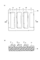
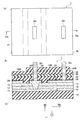
- A A plurality of (three in the example in the figure) schematic plan pattern configuration diagrams of the organic thin film solar cells according to the embodiment arranged in series, (b) along the line 57b-57b in FIG. 57
- FIG. 58 is a schematic cross-sectional structure diagram, (c) circuit representation corresponding to FIGS.
- FIG. 4 is a schematic plan pattern configuration showing a state in which a second electrode layer is patterned on a bulk heterojunction organic active layer, which is a step of a method for manufacturing an organic thin-film solar cell according to a third embodiment.
- FIG. 59B is a schematic sectional view taken along the line 58b-58b in FIG. It is one process of the manufacturing method of the organic thin-film solar cell which concerns on 3rd Embodiment, Comprising: (a) Excessive organic layer is etched by oxygen plasma processing, and an oxide film is formed in the surface of a 2nd electrode layer FIG.
- FIG. 60 is a schematic plane pattern configuration diagram showing the state obtained, (b) a schematic cross-sectional structure diagram taken along the line 59b-59b in FIG. 59 (a).
- FIG. 60A is a schematic plan pattern configuration diagram showing a state in which a passivation layer is formed on the entire surface of the device, which is a step of the manufacturing process of the organic thin-film solar cell according to the third embodiment.
- FIG. 5B is a schematic plan pattern configuration diagram showing a state where a colored barrier layer is formed on a passivation layer, which is a step of a manufacturing process of an organic thin-film solar cell according to a third embodiment.
- FIG. 60A is a schematic plan pattern configuration diagram showing a state in which a passivation layer is formed on the entire surface of the device, which is a step of the manufacturing process of the organic thin-film solar cell according to the third embodiment.
- FIG. 6 is a schematic plan pattern configuration diagram showing a state in which a backsheet passivation layer is formed on a colored barrier layer, which is a step of a manufacturing process of an organic thin film solar cell according to a third embodiment
- FIG. 62 is a schematic sectional view taken along the line 62b-62b in FIG. It is one process of the manufacturing process of the organic thin-film solar cell concerning 3rd Embodiment, Comprising: (a) Typical plane pattern block diagram which shows the state which formed the 1st through-hole and the 2nd through-hole, (b) FIG.
- FIG. 63 is a schematic sectional view taken along the line 63b-63b in FIG.
- the flowchart which shows the preparation procedure of the organic thin film solar cell which concerns on 3rd Embodiment.
- A A schematic plane pattern configuration diagram of an organic thin-film solar cell according to Modification 1 of the third embodiment,
- FIG. 5 is a schematic cross-sectional structure diagram showing a state in which an oxide film is formed on the surface of the second electrode layer by oxygen plasma treatment in one step of the method for manufacturing the organic thin-film solar cell according to the third embodiment.
- B The typical cross-section figure showing the state where the passivation layer was formed in the device whole surface
- c The typical cross-section figure showing the state where the colorization barrier layer was formed on the passivation layer.
- FIG. 6 is a schematic cross-sectional structure diagram showing a state in which a backsheet passivation layer is formed on a colored barrier layer, which is a step of a method for manufacturing an organic thin film solar cell according to a third embodiment;
- the typical cross-section figure which shows the state which formed the 1st through-hole and the 2nd through-hole. It is one process of the manufacturing method of the organic thin-film solar cell concerning 3rd Embodiment, Comprising: (a) Typical cross-section figure which shows the state in which the 1st terminal electrode and the 2nd terminal electrode were formed, (b) FIG. The enlarged view of A part of 69 (a).
- FIG. 71 is a schematic sectional view taken along the line 71-71 in FIG.
- FIG. 71 is a schematic sectional view taken along the line 72-72 in FIG.
- FIG. 73 is a schematic sectional view taken along the line 73-73 in FIG.
- A Schematic cross-sectional structure diagram of an electronic device having a tandem structure to which the organic thin film solar cell according to the third embodiment is applied
- (b) In-cell structure to which the organic thin film solar cell according to the third embodiment is applied The typical cross-section figure of the electronic device of.
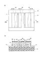
- FIG. 75 A schematic plane pattern configuration diagram of an organic thin-film solar cell according to Modification 2 of the third embodiment, (b) a schematic cross-sectional structure diagram taken along line 75b-75b of FIG. 75 (a), (c) ) Circuit representation corresponding to FIGS. 75 (a) and 75 (b).
- FIG. 75 A schematic plane pattern configuration diagram of an organic thin-film solar cell according to Modification 2 of the third embodiment, (b) a schematic cross-sectional structure diagram taken along line 75b-75b of FIG. 75 (a), (c) ) Circuit representation corresponding to FIGS. 75 (a) and 75 (b).
- FIG. 11 is a schematic cross-sectional structure diagram showing a state in which a transparent electrode layer is patterned on a substrate, which is a step of a method for manufacturing an organic thin-film solar cell according to Modification 2 of the third embodiment; ) A schematic cross-sectional structure diagram showing a state in which a hole transport layer is formed on a transparent electrode layer, (c) a schematic cross-sectional structure showing a state in which a bulk heterojunction organic active layer is formed on a hole transport layer
- FIG. 4D is a schematic cross-sectional view showing a state in which a third through hole that penetrates the hole transport layer and the bulk heterojunction organic active layer and reaches the first electrode layer is formed in a direction perpendicular to the substrate. Structural drawing.
- FIG. 4 is a schematic cross-sectional structure diagram showing a state in which a passivation layer, a colorization barrier layer, and a backsheet passivation layer are formed on the second electrode layer and the VIA electrode layer.
- “transparent” is defined as having a transmittance of about 50% or more. Further, “transparent” is also used to mean colorless and transparent with respect to visible light in the organic thin film solar cell according to the embodiment. Visible light corresponds to a wavelength of about 360 nm to 830 nm and an energy of about 3.45 eV to 1.49 eV, and is transparent if the transmittance is 50% or more in this region.
- the organic thin-film solar cell 1 includes a substrate 10, a transparent electrode layer (first electrode layer) 11 disposed on the substrate 10, and a first electrode layer 11.
- the hole transport layer 12 disposed above, the bulk heterojunction organic active layer 14 disposed on the hole transport layer 12, and the cathode electrode layer (second electrode layer) disposed on the bulk heterojunction organic active layer 14 16 and a sealing glass 40 that opposes the substrate 10 and seals a laminated structure including the first electrode layer 11, the hole transport layer 12, the bulk heterojunction organic active layer 14, and the second electrode layer 16;
- a glass frit 36 is provided between the sealing glass 40 and the substrate 10 and seals the laminated structure.
- the organic thin-film solar cell 1 has an organic layer (12, 14) having a thickness of about several hundreds of nanometers serving as a power generation layer on a glass substrate 10 with ITO.
- the second electrode layer 16 is formed by stacking and depositing a metal layer such as aluminum. Since pure aluminum formed as the second electrode layer 16 is easily oxidized, a passive film may be formed or a passivation film such as SiN or SiON may be laminated for durability.
- the glass frit 36 is disposed on the sealing glass 40. This is because organic layers such as the hole transport layer 12 and the bulk heterojunction organic active layer 14 are disposed on the substrate 10, so that these organic layers are not damaged when the glass frit is sintered at a high temperature. .
- a glass frit 36 can be formed by applying a glass frit paste that can be applied using a screen printing technique or a dispenser in an arbitrary pattern and baking at a high temperature.
- the height of the glass frit 36 is, for example, about 1 ⁇ m to about 100 ⁇ m, and the width of the glass frit 36 is, for example, about 0.2 mm to about 2.0 mm.
- a thermosetting resin or a UV curable resin can be applied.
- a UV curable resin a transparent glass frit that transmits ultraviolet rays may be used.
- a glass frit material having a high total ray transmittance (for example, 90% or more) with respect to UV light for example, a Zn-based glass can be applied.
- the glass frit can also be composed of Bi—B—Si based oxide powder. The glass frit made of this Bi—B—Si-based oxide has the property of absorbing heat and generating heat and melting. Therefore, it is possible to fuse the sintered body of the paste containing the glass frit by irradiating it with an infrared laser (for example, wavelength 1064 nm).
- the organic thin-film solar cell according to the first embodiment provides an oxygen (O 2 ) getter action by providing a gettering sheet desiccant 38GU on the inner wall surface of the sealing glass 40. May be increased.
- the gettering sheet desiccant for example, strontium oxide (SrO), calcium oxide (CaO), or the like can be used as an oxygen (O 2 ) -based getter agent.
- an engraved glass 40A is applied for sealing.
- the thickness of the outer shape of the digging glass 40A is, for example, about 0.7 mm, and the depth of the digging portion containing the element portion is, for example, about 0.3 mm.
- the digging glass 40A when digging an arbitrary pattern, it is necessary to create a mask plate for creating the digging for each pattern. Further, in order to form the digging portion, etching with hydrofluoric acid is required, which is expensive and troublesome.
- the sealing using the dug glass 40A is expensive, and the thickness of the module is thick and heavy.
- the sealing glass 40 and the transparent glass frit 36 fired on the sealing glass 40 are used for sealing.
- the sealing glass 40 for example, non-alkali tempered glass having a thickness of about 0.1 mm to 0.2 mm is applicable.
- the glass frit 36 is applied to the sealing glass 40 by applying a glass frit paste (organic solvent + glass frit) by screen printing, drying the organic solvent at about 100 ° C., and then at about 500 ° C. to 590 ° C. And sintered for about 30 minutes.
- the thickness of the glass frit 36 is, for example, about 5 ⁇ m to 20 ⁇ m.
- the thickness of the resin 36U for bonding the glass frit 36 and the substrate 10 is, for example, about 5 to 20 ⁇ m.
- the glass frit 36 can freely draw a pattern by using dispenser coating, and can be formed on the sealing glass 40 without using dangerous chemicals. Moreover, the module of the organic thin film solar cell according to the embodiment can be further reduced in weight and thickness by using a relatively thin cover glass (sealing glass 40) as compared with the dug glass 40A.
- FIG. 4 A schematic diagram illustrating the operating principle of the organic thin-film solar cell 1A is expressed as shown in FIG. Moreover, the energy band structure of the various materials of the organic thin film solar cell 1A shown in FIG. 4 is expressed as shown in FIG. With reference to FIG. 4 and FIG. 5, the principle structure and operation
- the organic thin-film solar cell 1 ⁇ / b> A includes a substrate 10, a transparent electrode layer 11 disposed on the substrate 10, a hole transport layer 12 disposed on the transparent electrode layer 11, A bulk heterojunction organic active layer 14 disposed on the hole transport layer 12 and a second electrode layer 16 disposed on the bulk heterojunction organic active layer 14 are provided.
- the second electrode layer 16 is made of, for example, aluminum (Al) and serves as a cathode electrode layer.
- the bulk heterojunction organic active layer 14 includes a p-type organic active layer region and an n-type organic active layer region, as shown in the right diagram of FIG. 4, and forms a complex bulk hetero pn junction.
- the p-type organic active layer region is formed of, for example, P3HT (poly (3-hexylthiophene-2,5diyl)), and the n-type organic active layer region is, for example, PCBM (6,6-phenyl-C61-). butyric acid methyl ester).
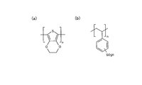
- PEDOT PSS applied to the hole transport layer 12 in the organic thin film solar cell 1A, the chemical structural formula of PEDOT is expressed as shown in FIG. 6A, and the chemical structural formula of PSS is shown in FIG. It is expressed as shown in b).
- examples of chemical structural formulas of materials used in vacuum deposition are as follows. That is, an example of phthalocyanine (Pc) is represented as shown in FIG. 8A, and an example of zinc phthalocyanine (ZnPc: Zinc-phthalocyanine) is represented as shown in FIG.
- An example of -Ptcdi N, N'-dimethyl perylene-3,4,9,10-dicarboximide
- an example of fullerene (C 60 : Buckminster fullerene) is shown in FIG. It is expressed as shown in FIG.
- Examples of chemical structural formulas of materials used in the solution process in the organic thin film solar cell 1A are as follows. That is, an example of MDMO-PPV (poly [2-methoxy-5- (3,7-dimethyl-octyloxy)]-1,4-phenylene-vinylene) is represented as shown in FIG. An example of PFB (poly (9,9′-dioctylfluorene-co-bis-N, N ′-(4-butylphenyl) -bis-N, N′-phenyl-1,4-phenylenediamine) is shown in FIG. 9 (b).
- MDMO-PPV poly [2-methoxy-5- (3,7-dimethyl-octyloxy)]-1,4-phenylene-vinylene
- PFB poly (9,9′-dioctylfluorene-co-bis-N, N ′-(4-butylphenyl) -bis-N, N′-pheny
- FIG. c An example of CN-MDMO-PPV (poly- [2-methoxy-5- (2'-ethylhexyloxy) -1,4- (1-cyanovinylene) -phenylene]) is shown in FIG. c) PFO-DBT (poly [2,7- (9,9-dioctyl-fluorene) -alt-5,5- (4,7'-di-2-thienyl-2 ') , 1 ′, 3′-benzothiadiazole)]) is represented as shown in FIG.
- F8BT poly (9,9′-dioctyl fluoreneco-benzothiadiazole)
- FIG. 1 An example of carbazole-alt-5,5- (4 ′, 7′-di-thienyl-2′1 ′, 3′-b3nzothiadizaole)]) is represented as shown in FIG.
- PC 60 BM (6,6-phenyl-C61-butyric acid methyl ester) is represented as shown in FIG. 9 (g), and PC 70 BM (6,6-phenyl-C71-butyric acid methyl ester).
- ester An example of ester is represented as shown in FIG.
- the stacked structure portion of the organic thin-film solar cell 1 includes a substrate 10, a transparent electrode layer (first electrode layer) 11 disposed on the substrate 10, A hole transport layer 12 disposed on one electrode layer 11, a bulk heterojunction organic active layer 14 disposed on the hole transport layer 12, and a cathode electrode layer (first layer disposed on the bulk heterojunction organic active layer 14); 2 electrode layer) 16.
- the laminated structure portion of the organic thin film solar cell 1 according to the modification of the first embodiment further includes a passive film 24 disposed on the surface of the second electrode layer 16 as shown in FIG.
- the passive film 24 is composed of an oxide film of the second electrode layer 16.
- the oxide film of the second electrode layer 16 can be formed by performing oxygen plasma treatment on the surface of the second electrode layer 16.
- the thickness of the passivation film 24 is, for example, about 10 angstroms to about 100 angstroms.
- omitted you may provide the passivation film arrange
- This passivation film can be composed of, for example, a SiN film or a SiON film.
- the second electrode layer 16 may be made of any one of Al, W, Mo, Mn, and Mg.
- the passive film 24 is an alumina (Al 2 O 3 ) film.
- the organic thin-film solar cell 1 including the passive film 24 on the surface of the second electrode layer 16 has a second structure even when moisture or oxygen penetrates into the bulk heterojunction organic active layer 14. It is possible to prevent the electrode layer 16 from being oxidized by the moisture and oxygen. Thereby, deterioration of an organic solar cell can be suppressed and durability can be improved.
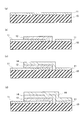
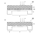
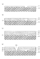
- a process for preparing an ITO substrate in which the transparent electrode layer 11 is formed on the substrate 10 is a process of the method for manufacturing the organic thin-film solar cell according to the first embodiment.
- the step of patterning the hole transport layer 12 on the transparent electrode layer 11 after patterning the transparent electrode layer 11 is represented as shown in FIG.
- the step of patterning the heterojunction organic active layer 14 is expressed as shown in FIG. 12C, and the step of patterning the second electrode layer 16 on the bulk heterojunction organic active layer 14 is shown in FIG. It is expressed as shown in d).
- FIG. 13 is a process of manufacturing the organic thin film solar cell according to the first embodiment, and the process of preparing the sealing glass 40 is expressed as shown in FIG.
- the step of forming the glass frit 36 is represented as shown in FIG. 13B, and the step of forming the resin 36U at the tip portion of the glass frit 36 is represented as shown in FIG.
- the method of manufacturing the organic thin-film solar cell 1 according to the first embodiment includes a step of preparing a substrate 10 and a step of forming a first electrode layer 11 on the substrate 10 as shown in FIGS.
- a step of forming a glass frit 36 on the sealing glass 40 a step of forming a resin 36 U at the tip of the glass frit 36, a glass frit with the sealing glass 40 and the substrate 10 facing each other.
- 36 and a resin 36U to seal the laminated structure including the first electrode layer 11, the hole transport layer 12, the bulk heterojunction organic active layer 14, and the second electrode layer 16.
- a transparent electrode layer 11 made of, for example, ITO is formed on a substrate 10.
- the hole transport layer 12 is patterned on the transparent electrode layer 11.
- a wet etching technique an oxygen plasma etching technique, a laser patterning technique, a nanoimprint technique, and the like can be applied.
- a spin coating technique, a spray technique, a screen printing technique, or the like can be applied.
- PEDOT: PSS is formed by spin coating, and annealing is performed at 120 ° C. for about 10 minutes in order to remove moisture.
- a bulk heterojunction organic active layer 14 to be a power generation layer is formed on the hole transport layer 12.
- P3HT is formed by spin coating.
- heating is performed at about 100 ° C. to 120 ° C. for about 10 minutes to 30 minutes in order to dry the organic solvent. .
- the cathode electrode layer 16 is formed on the bulk heterojunction organic active layer 14.
- a metal layer such as Al, W, Mo, Mn, and Mg can be formed by a vacuum heating deposition method. Further, screen printing technology may be applied.
- a sealing glass 40 is prepared.
- the sealing glass 40 for example, non-alkali tempered glass having a thickness of about 0.1 mm to 0.2 mm is applicable.
- a glass frit 36 is formed on the sealing glass 40.
- the glass frit 36 is formed by applying a glass frit paste (organic solvent + glass frit) to the sealing glass 40 by screen printing, drying the organic solvent at about 100 ° C., and about 500 ° C. to 590 ° C. It is formed by sintering for 30 minutes.
- the thickness of the glass frit 36 is, for example, about 5 ⁇ m to 20 ⁇ m.
- the glass frit 36 can freely draw a pattern by using dispenser coating, and can be formed on the sealing glass 40 without using dangerous chemicals.
- thermosetting resin is desirably a temperature that does not damage the hole transport layer 12 and the bulk heterojunction organic active layer 14, for example, about 100 ° C. to about 120 ° C. or less.
- the entire device is sealed with a sealing glass (cover glass) 40, a glass frit 36, and a resin 36U.
- the glass frit 36 and the transparent electrode layer (ITO) 11 are bonded by the resin 36U.
- the sealing step is preferably performed in a nitrogen atmosphere in order to prevent deterioration due to moisture and oxygen in the air.
- the organic thin-film solar cell 1 according to the first embodiment can be obtained.
- an oxide film (passive film) 24 may be formed on the surface of the second electrode layer 16.
- the passive film 24 can be formed by subjecting the second electrode layer 16 to oxygen plasma treatment. The excess organic layer is removed by oxygen plasma, and an oxide film treatment is performed on the aluminum resurface.
- a silicon nitride film or the like may be formed on the aluminum surface as a passivation film by a chemical vapor deposition method (CVD: Chemical Vapor Deposition).
- the thickness of the silicon nitride film is, for example, about 0.5 ⁇ m to 1.5 ⁇ m. Durability can be further improved by protecting the inner element with a silicon nitride film.
- a gettering sheet desiccant 38GU may be provided on the inner wall surface of the sealing glass 40 to further eliminate the influence of moisture and oxygen.
- UV irradiation when curing the UV curable resin 36U, UV irradiation, it may be carried out from the sealing glass 40 side. This is because aluminum becomes a reflective layer against UV irradiation, so that the element portion can be protected.
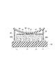
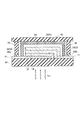
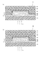
- the sealing part in the organic thin film solar cell according to the first embodiment may have a configuration in which a glass frit 36 is covered with a UV curable resin 36U as shown in FIG. Furthermore, as shown in FIG. 15B, the sealing portion in the organic thin film solar cell according to the embodiment is such that the glass frit 36 is covered with the UV curable resin 36U, and the contact between the UV curable resin 36U and the substrate 10 is achieved. You may provide the structure which increased the area compared with the structure of Fig.15 (a).
- the sealing part in the organic thin film solar cell according to the first embodiment may have a configuration in which a porous glass frit 36P is covered with a UV curable resin 36U as shown in FIG. . That is, a porous glass frit may be used. When the porous glass frit 36P is applied, the resin 36U penetrates into the glass frit 36P and the “anchor effect” works, so that stronger adhesion can be realized.
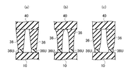
- the glass frit 36 in the organic thin film solar cell according to the first embodiment may have a wedge-shaped shape, a tapered shape, or a spindle-shaped tapered shape in which the cross-sectional area decreases as the distance from the sealing glass 40 increases. .
- a plurality of glass frit 36 may be formed.
- FIG. 17A shows a configuration example of the sealing portion of the organic thin film solar cell according to the first embodiment, in which two formed glass frits 36 have a wedge shape. Moreover, the structural example in which the two glass frit 36 formed has a taper shape is represented as shown in FIG. In addition, a configuration example in which the cross-sectional shape of the two formed glass frit 36 has a spindle-shaped taper shape in which the cross-sectional area decreases as the distance from the sealing glass 40 increases is expressed as shown in FIG.
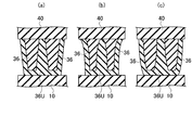
- a configuration example in which two formed glass frits 36 have a wedge shape and are covered with a UV curable resin 36U is as follows. It is expressed as shown in FIG. Further, a configuration example in which the two formed glass frit 36 has a tapered shape and is covered with the UV curable resin 36U is expressed as shown in FIG. Further, a configuration example in which the cross-sectional shape of the two formed glass frit 36 has a spindle-shaped taper shape in which the cross-sectional area becomes smaller as the distance from the sealing glass 40 is reduced, and the configuration example is covered with the UV curable resin 36 is shown in FIG. It is expressed as shown in (c).
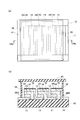
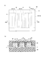
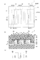
- FIG. 19A A schematic cross-sectional structure taken along line 19b-19b in FIG. 19A is expressed as shown in FIG.
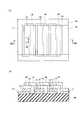
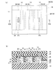
- FIG. 20 (a) a schematic plane pattern configuration showing a state in which the hole transport layer 12 is formed on the transparent electrode layer 11 is expressed as shown in FIG. 20 (a), and is shown by a line 20b-20b in FIG. 20 (a).
- the schematic cross-sectional structure along is represented as shown in FIG.
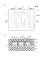
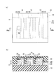
- FIG. 21 (a) a schematic planar pattern configuration showing a state in which the bulk heterojunction organic active layer 14 is formed on the hole transport layer 12 is expressed as shown in FIG. 21 (a), and 21b in FIG. 21 (a).
- FIG. 21 (a) a schematic planar pattern configuration showing a state in which the bulk heterojunction organic active layer 14 is formed on the hole transport layer 12 is expressed as shown in FIG. 21 (a), and 21b in FIG. 21 (a).
- a schematic cross-sectional structure along the line -21b is expressed as shown in FIG.
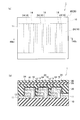
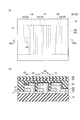
- FIG. 1 A schematic planar pattern configuration showing a state in which the second electrode layer 16 is formed on the bulk heterojunction organic active layer 14 is expressed as shown in FIG.
- FIG. 1 A schematic cross-sectional structure along the line 22b is expressed as shown in FIG.
- FIG. 23A A schematic plane pattern configuration showing a state in which the (film) 24 is formed is expressed as shown in FIG. 23A, and a schematic cross-sectional structure taken along line 23b-23b in FIG. 23A is shown in FIG. ).
- FIG. 24 (a) A schematic cross-sectional structure along the line is expressed as shown in FIG.
- a glass substrate 10 for example, length of about 50 mm ⁇ width of about 50 mm ⁇ thickness of about 10.4 mm
- a glass substrate 10 washed with pure water, acetone, and ethanol is placed in an ICP etcher, and the surface of the substrate is clarified by O 2 plasma. Remove deposits (glass substrate surface treatment).
- a glass substrate 10 washed with pure water, acetone, and ethanol is placed in an ICP etcher, and the surface of the substrate is clarified by O 2 plasma. Remove deposits (glass substrate surface treatment).
- the transparent electrode layer 11 made of, for example, ITO is formed on the glass substrate 10.
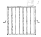
- a plurality of transparent electrode layers 11 are formed in a stripe pattern across the groove.
- An oxygen plasma etching technique, a laser patterning technique, a nanoimprint technique, or the like can be applied to the formation of the groove.
- the hole transport layer 12 is formed on each transparent electrode layer 11.
- a spin coating technique, a spray technique, a screen printing technique, or the like can be applied.
- PEDOT: PSS is formed by spin coating, and annealing is performed at 120 ° C. for about 10 minutes to remove moisture.
- An oxygen plasma etching technique, a laser patterning technique, a nanoimprint technique, or the like can be applied to the formation of the groove.
- a bulk heterojunction organic active layer 14 is formed on each hole transport layer 12.
- P3HT is formed by spin coating.
- the cathode electrode layer 16 is formed on each bulk heterojunction organic active layer 14.
- the cathode electrode layer 16 is formed, for example, by depositing a metal layer such as Al, W, Mo, Mn, and Mg by a vacuum heating vapor deposition method.
- a screen printing technique may be applied instead of the vacuum heating deposition method.
- an oxide film (passive film) 24 is formed on the surface of the cathode electrode layer 16.
- Each cell can be separated by etching the bulk heterojunction organic active layer 14 and the hole transport layer 12.
- the passive film 24 can be formed by subjecting the second electrode layer 16 to oxygen plasma treatment.
- the passive film 24 can be formed using, for example, a high-density plasma etching apparatus.
- the entire device is sealed with a sealing glass (cover glass) 40 and a glass frit 36 / UV curable resin 36U.
- the glass frit 36 and the transparent electrode layer (ITO) 11 are bonded by the UV curable resin 36U.
- the sealing step is preferably performed in a nitrogen atmosphere in order to prevent deterioration due to moisture and oxygen in the air.
- a gettering sheet desiccant 38GU may be provided on the inner wall surface of the sealing glass 40 to further eliminate the influence of moisture and oxygen.
- the organic thin-film solar cell 1 according to the embodiment can be obtained.
- FIG. 24 a schematic cross-sectional structure example showing a state in which the sealing glass 40 is bent is expressed as shown in FIG.
- the sealing glass 40 is bent, the cells constituting the organic thin-film solar battery are crushed and a short-circuit state may occur between the anode electrode layer 11 and the cathode electrode layer 16.
- the cover glass 40 or the substrate 10 is bent by pressure from the outside, so that the cover glass 40 does not come into contact with an internal element and is not damaged.
- a glass support 18 may be provided.
- the glass support 18 can be formed in the same manner as the glass frit 36.
- the configuration example 1 that includes the glass support base 18 inside the sealing glass 40 and can suppress the bending of the sealing glass 40 is illustrated in FIG. ).
- Another configuration example 2 is expressed as shown in FIG.
- the structural example 3 which can provide the glass support stand 18 inside the sealing glass 40, and can suppress the bending of the sealing glass 40 is FIG.
- Another configuration example 4 is represented as shown in FIG. 27B.
- the glass support 18 may be disposed in contact with the second electrode layer 16 as shown in FIG.
- the glass support 18 may be disposed in contact with the first electrode layer 11B between adjacent cells as shown in FIGS. 26 (b), 27 (a), and 27 (b).
- the first electrode layer 11A represents the transparent electrode layer of the left cell of the adjacent cell
- the first electrode layer 11B represents the transparent electrode layer of the right cell of the adjacent cell.
- the glass support base 18 may be disposed between a plurality of cells.
- the glass support 18 can be formed so as to have a dot pattern or a stripe pattern on the surface of the substrate 10.
- the gettering sheet desiccant 38GU / 38GS is disposed inside the substrate 10 and the sealing glass 40.
- gettering sheet desiccant 38GU can be disposed on the inner wall surface of the sealing glass 40 facing the substrate 10.
- gettering sheet desiccant 38GS can be disposed on the substrate 10 and the inner substrate 10 sealed with the sealing glass 40.
- Each cell includes a substrate 10, an anode electrode layer 11 disposed on the substrate 10, a hole transport layer 12 disposed on the anode electrode layer 11, and a bulk heterojunction organic disposed on the hole transport layer 12.
- An active layer 14 and a cathode electrode layer 16 disposed on the bulk heterojunction organic active layer 14 are provided. Further, the entire seven cells are hollow sealed with sealing glass 40, glass frit 36, and UV curable resin 36U.
- a gettering sheet desiccant 38GU is disposed on the inner wall surface of the sealing glass 40.
- a passive film is formed on the surface of the cathode electrode layer 16.
- the anode electrode layer 11 (A1) is connected to the anode terminal A
- the cathode electrode layer 16 (K1) is connected to the anode electrode layer 11 (A2) at the cell periphery.
- the cathode electrode layer 16 (K2) is connected to the anode electrode layer 11 (A3) at the cell periphery
- the cathode electrode layer 16 (K6) is connected to the anode electrode layer 11 (A7) and the cell periphery.
- the cathode electrode layer 16 (K7) is connected to the first electrode layer 11 (K1) at the cell periphery
- the first electrode layer 11 (K1) is connected to the cathode terminal K.
- a glass support for preventing bending may be provided on the inner wall surface of the sealing glass 40 facing the substrate 10.
- the glass support may be disposed in contact with the second electrode layer, or may be disposed in contact with the first electrode layer.
- the glass support base may be arranged between a plurality of cells.
- step S ⁇ b> 1 PEDOT: PSS is applied on the substrate 10.
- the PEDOT: PSS aqueous solution is filtered with a 0.45 ⁇ m PTFE membrane filter to remove undissolved residues and impurities, and the PEDOT: PSS aqueous solution is applied onto the ITO substrate 10 and spin-coated (for example, 4000 rpm, 30 sec).
- step S2 PEDOT: PSS is sintered. That is, after film formation, heat treatment is performed at 120 ° C. for 10 minutes to remove moisture. In addition, it is good to cover the petri dish previously warmed with the hot plate so that heat may be transmitted to the whole substrate 10.
- step S3 P3HT: PCBM is applied. Specifically, for example, 16 mg of P3HT and 16 mg of PCBM are dissolved in dichlorobenzene (o-dichlorobenzen). The solution is stirred overnight at 50 ° C. in a nitrogen atmosphere and then sonicated at 50 ° C. for 1 minute. The solution is spin-coated on the ITO substrate 10 cleaned in a nitrogen-substituted glove box ( ⁇ 1 ppm O 2 , H 2 O). The number of rotations is, for example, 2000 rpm ⁇ 1 sec after 550 rpm ⁇ 60 sec.
- step S4 pre-annealing is performed. That is, after the application in step S3, heating is performed at 120 ° C. for 10 minutes. In addition, it is good to cover the petri dish previously warmed with the hot plate so that heat may be transmitted to the whole substrate 10.
- step S5 LiF vacuum deposition is performed. Specifically, LiF (purity: 99.98%) is subjected to vacuum heating deposition with a degree of vacuum: 1.1 ⁇ 10 ⁇ 6 torr ⁇ deposition rate of 0.1 ⁇ / sec.
- step S6 the second electrode layer 16 is formed by performing Al vacuum deposition. Specifically, Al (purity: 99.999%) is subjected to vacuum heating deposition with a degree of vacuum: 1.1 ⁇ 10 ⁇ 6 torr and a deposition rate of ⁇ 2 ⁇ / sec.
- step S7 an electrode oxide film treatment is performed on the second electrode layer 16.
- the oxide film 24 is formed by oxidizing the surface of the second electrode layer 16 with oxygen plasma using a high-density plasma etching apparatus.
- step S8 sealing is performed. Specifically, using a sealing glass on which a glass frit is formed, a UV curable resin is formed on the tip of the glass frit, facing the substrate, and exposed for about 10 minutes in a UV oven, for example. Seal.
- the organic thin-film solar cell according to the first embodiment can be manufactured by arranging a plurality of cells in a matrix and performing a mass production process.
- the transparent electrode layer 11 made of, for example, ITO is formed on the substrate 10.
- the transparent electrode layer 11 is formed in two stripe patterns with a gap therebetween.
- an oxygen plasma etching technique, a laser patterning technique, a nanoimprint technique, or the like can be applied.
- the hole transport layer 12 is formed on the substrate 10 and the transparent electrode layer 11.
- a spin coating technique, a spray technique, a screen printing technique, or the like can be applied.
- PEDOT: PSS is formed by spin coating, and annealing is performed at 120 ° C. for about 10 minutes to remove moisture.
- a bulk heterojunction organic active layer 14 is formed on the hole transport layer 12.
- P3HT: PCBM is formed by spin coating.
- the thickness of the bulk heterojunction organic active layer 14 is, for example, about 100 nm to about 200 nm.
- the cathode electrode layer 16 is formed, for example, by depositing Al, W, Mo, Mn, Mg or the like by a vacuum heating vapor deposition method.
- a screen printing technique may be applied instead of the vacuum heating deposition method.
- an oxide film (passive film) is formed on the surface of the cathode electrode layer 16.
- the passive film can be formed by exposing the cathode electrode layer 16 to oxygen plasma. Formation of the oxide film by oxygen plasma can be performed using, for example, a plasma etching apparatus.
- sealing glass cover glass
- glass frit glass frit
- the organic thin-film solar cell 1 according to the embodiment can be mass-produced.
- FIG. 1 a schematic plane pattern configuration example in which a plurality of cells C ij are arranged in a matrix is expressed as shown in FIG.
- Cells... C ij are arranged at the intersections of the cathode electrode patterns..., K i ⁇ 1 , K i , K i + 1 ,.
- the cathode electrode pattern ..., K i-1 , K i , K i + 1 , ... cells arranged at the intersections ... C It is also possible to separately measure the characteristics of ij .
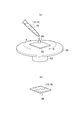
- a spin coating method as shown in FIG. 37 (a) can be applied.
- a spin coater including a spindle 62 that can be rotated at a high speed and connected to a driving source such as a motor, and a table 63 that is fixed to the spindle 62 and places the substrate 10 thereon is used. It is done.
- the substrate 10 is placed on the table 63, a driving source such as a motor is operated, and the table 63 is rotated at a high speed in the directions of arrows A and B, for example, at 2000 to 4000 rpm.
- a solution droplet 64 that forms the hole transport layer 12 and the bulk heterojunction organic active layer 14 is dropped.
- the droplet 64 can form the positive hole transport layer 12 and the bulk heterojunction organic active layer 14 (refer FIG.37 (b)) of uniform thickness on the board
- an organic thin-film solar cell that is inexpensive, has improved durability, and can be reduced in weight and thickness, and a method for manufacturing the same.
- the organic thin-film solar cell 1 includes a substrate 10, a transparent electrode layer (first electrode layer) 11 disposed on the substrate 10, and a first A hole transport layer 12 disposed on the electrode layer 11, a bulk heterojunction organic active layer 14 disposed on the hole transport layer 12, and a cathode electrode layer (second second layer disposed on the bulk heterojunction organic active layer 14) Electrode layer) 16, passivation layer 26 disposed on second electrode layer 16, colored barrier layer 28 disposed on passivation layer 26, and backsheet passivation layer disposed on colored barrier layer 28. 30.
- the organic thin-film solar cell 1 ⁇ / b> B according to the comparative example is on the substrate 10, the transparent electrode layer (first electrode layer) 11 disposed on the substrate 10, and the first electrode layer 11. , A hole heterojunction organic active layer 14 disposed on the hole transport layer 12, and a cathode electrode layer (second electrode layer) 16 disposed on the bulk heterojunction organic active layer 14.
- a backsheet layer 33 is disposed on the substrate 10, the transparent electrode layer (first electrode layer) 11 disposed on the substrate 10, and the first electrode layer 11.
- a hole heterojunction organic active layer 14 disposed on the hole transport layer 12, and a cathode electrode layer (second electrode layer) 16 disposed on the bulk heterojunction organic active layer 14.
- the barrier layer 29 is formed by laminating an inorganic passivation film such as SiN or SiON and a resin protective film in multiple layers by a chemical vapor deposition (CVD) method.
- the transparent resin material used as the resin protective film was transparent except for the cell portion. Therefore, when coloring the module according to the intended use, it is necessary to add extra materials such as attaching a color film as the backsheet layer 33. There is.
- a white or black back sheet is bonded to the back of the module.
- the use of the backsheet layer 33 increases the thickness of the module and increases the cost.
- the organic thin-film solar cell 1 according to the second embodiment is thinner than the comparative example by using a protective film (colored barrier layer 28) to which a colorant is added.
- the module structure enables the module to be arbitrarily colored. That is, by using a color filter capable of arbitrary patterning by UV irradiation for the protective layer of the cell, the protective layer has a design property, and the manufacturing process can be reduced and the design property can be improved as compared with the comparative example. Yes.
- the organic thin-film solar cell 1 has an organic layer (12 ⁇ 12) having a thickness of about several hundreds of nanometers serving as a power generation layer on the glass substrate 10 with ITO. 14) are laminated, and a metal layer such as aluminum is deposited as the second electrode layer 16 by vapor deposition.
- a passive film 24 may be formed as shown in FIG.
- organic layers such as the hole transport layer 12 and the bulk heterojunction organic active layer 14 are disposed on the substrate 10, when the passivation layer 26 is formed by forming the passivation film 24, these organic layers are formed on the organic layer. It is possible to prevent damage.
- the colored barrier layer 28 disposed on the passivation layer 26 serves as a protective layer for the cells of the organic thin-film solar cell 1 according to the embodiment.
- the colored barrier layer 28 can be formed of a color filter that can be patterned arbitrarily by ultraviolet (UV) irradiation.
- UV ultraviolet
- the organic thin-film solar cell 1 according to the embodiment can impart design properties to the protective layer, and a comparative example (FIG. 38B). Rather, it can reduce the number of manufacturing steps and improve the design.
- the passivation layer 26 and the colored barrier layer 28 can be formed by laminating an inorganic passivation film such as SiN or SiON by CVD and a resin protective film in multiple layers. is there.
- the organic thin film solar cell 1 in order to enable coloring without changing the module process, by adding a dye to the material of the resin protective film, The part can be colored in an arbitrary color. Since this resin material can leave a pattern only in a portion irradiated with UV after coating and forming, it is possible to perform a color scheme on the back with an arbitrary pattern.
- colorant for example, carbon black, blue, for example, phthalocyanine-based paints, and red, for example, alizarin-based paints can be applied.
- the operation principle and the constituent materials of the respective parts are the same as those in the first embodiment, and thus the duplicated explanation is omitted.
- the laminated structure portion of the organic thin-film solar cell 1 includes a substrate 10, a transparent electrode layer (first electrode layer) 11 disposed on the substrate 10, A hole transport layer 12 disposed on one electrode layer 11, a bulk heterojunction organic active layer 14 disposed on the hole transport layer 12, and a cathode electrode layer (first layer disposed on the bulk heterojunction organic active layer 14); 2 electrode layer) 16.
- the laminated structure portion of the organic thin-film solar cell 1 according to the modification of the second embodiment further includes a passive film 24 disposed on the surface of the second electrode layer 16 as shown in FIG.
- the passive film 24 is composed of an oxide film of the second electrode layer 16.
- the oxide film of the second electrode layer 16 can be formed by performing oxygen plasma treatment on the surface of the second electrode layer 16.
- the thickness of the passivation film 24 is, for example, about 10 angstroms to about 100 angstroms.
- omitted you may provide the passivation film arrange
- This passivation film can be composed of, for example, a SiN film or a SiON film.
- the second electrode layer 16 may be made of any one of Al, W, Mo, Mn, and Mg.
- the passive film 24 is an alumina (Al 2 O 3 ) film.
- the organic thin-film solar cell 1 including the passive film 24 on the surface of the second electrode layer 16 has the second structure even when moisture or oxygen enters the bulk heterojunction organic active layer 14. It is possible to prevent the electrode layer 16 from being oxidized by the moisture and oxygen. Thereby, deterioration of an organic solar cell can be suppressed and durability can be improved.
- a process for preparing an ITO substrate in which the transparent electrode layer 11 is formed on the substrate 10 is a process of the method for manufacturing the organic thin film solar cell according to the second embodiment.
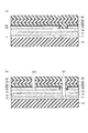
- the step of patterning the hole transport layer 12 on the transparent electrode layer 11 after patterning the transparent electrode layer 11 is represented as shown in FIG.
- the step of patterning the heterojunction organic active layer 14 is expressed as shown in FIG. 41C, and the step of patterning the second electrode layer 16 on the bulk heterojunction organic active layer 14 is shown in FIG. It is expressed as shown in d).
- FIG. 42B a process of forming the passive film (oxide film) 24 on the surface of the second electrode layer 16 as a process of the method for manufacturing the organic thin film solar cell according to the embodiment is illustrated in FIG.
- the step of forming the passivation layer 26 on the entire surface of the device is expressed as shown in FIG. 42B, and the step of forming the colored barrier layer 28 on the passivation layer 26 is shown in FIG. Represented as shown.
- the method for manufacturing the organic thin-film solar cell 1 includes the step of preparing the substrate 10 and the formation of the first electrode layer 11 on the substrate 10.
- the transparent electrode layer 11 made of, for example, ITO is formed on the substrate 10.
- the hole transport layer 12 is patterned on the transparent electrode layer 11.
- a wet etching technique an oxygen plasma etching technique, a laser patterning technique, a nanoimprint technique, and the like can be applied.
- a spin coating technique, a spray technique, a screen printing technique, or the like can be applied.
- PEDOT: PSS is formed by spin coating, and annealing is performed at 120 ° C. for about 10 minutes in order to remove moisture.
- a bulk heterojunction organic active layer 14 to be a power generation layer is formed on the hole transport layer 12.
- P3HT is formed by spin coating.
- heating is performed at about 100 ° C. to 120 ° C. for about 10 minutes to 30 minutes in order to dry the organic solvent. .
- the cathode electrode layer 16 is patterned on the bulk heterojunction organic active layer 14.
- a metal layer such as Al, W, Mo, Mn, and Mg can be formed by a vacuum heating deposition method. Further, screen printing technology may be applied.
- an oxide film (passive film) 24 is formed on the surface of the second electrode layer 16.
- the passive film 24 can be formed by subjecting the second electrode layer 16 to oxygen plasma treatment. The excess organic layer is removed by oxygen plasma, and an oxide film treatment is performed on the aluminum resurface.
- the passivation layer 26 is formed on the second electrode layer 16.
- a silicon nitride film or the like may be formed by a CVD method.
- the thickness of the silicon nitride film is, for example, about 0.5 ⁇ m to 1.5 ⁇ m.
- durability can be further improved by sealing with a SiN film formed by CVD.
- a colored barrier layer 28 is formed on the passivation layer 26.
- a UV curable resin material is applied by a spin coat method or the like and cured by UV irradiation.
- the colored barrier layer 28 uses a protective film to which a colorant is added, so that the module can be arbitrarily colored with a thinned element structure.
- a backsheet passivation layer 30 is formed on the colored barrier layer 28.
- a silicon nitride film or the like may be formed by a CVD method.
- the thickness of the silicon nitride film is, for example, about 0.5 ⁇ m to 1.5 ⁇ m.
- durability can be further improved by sealing with a SiN film formed by CVD.
- the organic thin-film solar cell 1 according to the embodiment can be completed.
- a step of forming a passivation layer 26 such as a silicon nitride film (FIG. 42B), a step of forming a colored barrier layer 28 on the passivation layer 26 (FIG. 42C). )) May be repeated to form a multi-layered protective film.
- the opening of the cell is arbitrarily patterned by an ink jet method or the like.
- the coloring barrier layer 28 (resin protective film) to which a dye is added can also be subjected to arbitrary patterning by using an inkjet method or the like.
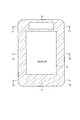
- the opening portion of the cell corresponds to, for example, the display region 2 or the character formation region 6 (see FIGS. 47 to 50).
- a schematic planar pattern configuration showing a state in which the transparent electrode layer 11 is formed on the substrate 10 in one step of the method for manufacturing the organic thin-film solar cell according to the second embodiment is the same as that in FIG.
- a schematic cross-sectional structure taken along line 19b-19b of FIG. 19A is represented in the same manner as FIG. 19B.
- FIG. 20A a schematic plane pattern configuration showing a state in which the hole transport layer 12 is formed on the transparent electrode layer 11 is expressed in the same manner as in FIG. 20A, and is along the line 20b-20b in FIG.
- a schematic cross-sectional structure is represented in the same manner as in FIG.
- FIG. 1 A schematic planar pattern configuration showing a state in which the bulk heterojunction organic active layer 14 is formed on the hole transport layer 12 is expressed in the same manner as in FIG.
- a schematic cross-sectional structure along the line 21b is represented in the same manner as in FIG.
- FIG. 22A a schematic planar pattern configuration showing a state in which the second electrode layer 16 is formed on the bulk heterojunction organic active layer 14 is expressed in the same manner as FIG. 22A, and 22b-22b in FIG. 22A.
- a schematic cross-sectional structure along the line is expressed in the same manner as in FIG.
- FIG. 43A A schematic planar pattern configuration showing a state in which the (film) 24 is formed is expressed as shown in FIG. 43A, and a schematic cross-sectional structure taken along line 43b-43b in FIG. 43A is shown in FIG. ).
- FIG. 44A a schematic plane pattern configuration showing a state in which the passivation layer 26 is formed on the entire surface of the device is represented as shown in FIG. 44A, and a schematic cross-sectional structure taken along line 44b-44b in FIG. 44 (b).
- FIG. 45A a schematic plane pattern configuration showing a state in which the colored barrier layer 28 is formed on the passivation layer 26 is expressed as shown in FIG. 45A, and is a schematic diagram along the line 45b-45b in FIG. 45A.
- a typical cross-sectional structure is represented as shown in FIG.
- FIG. 46A a schematic plane pattern configuration showing a state in which the backsheet passivation layer 30 is formed on the colored barrier layer 28 is expressed as shown in FIG. 46A, and is shown by the lines 46b-46b in FIG. 46A.
- FIG. 46A A schematic cross-sectional structure along the line is expressed as shown in FIG.
- FIGS. 19 to 22 and FIGS. 43 to 46 a method of manufacturing an organic thin film solar cell according to an embodiment in which a plurality (three in the example in the figure) are arranged in series will be described.
- a glass substrate 10 for example, length of about 50 mm ⁇ width of about 50 mm ⁇ thickness of about 10.4 mm
- a glass substrate 10 washed with pure water, acetone, and ethanol is placed in an ICP etcher, and the surface of the substrate is clarified by O 2 plasma. Remove deposits (glass substrate surface treatment).
- a glass substrate 10 washed with pure water, acetone, and ethanol is placed in an ICP etcher, and the surface of the substrate is clarified by O 2 plasma. Remove deposits (glass substrate surface treatment).
- the transparent electrode layer 11 made of, for example, ITO is formed on the glass substrate 10.
- a plurality of transparent electrode layers 11 are formed in a stripe pattern with a groove portion interposed therebetween.
- An oxygen plasma etching technique, a laser patterning technique, a nanoimprint technique, or the like can be applied to the formation of the groove.
- the hole transport layer 12 is formed on each transparent electrode layer 11.
- a spin coating technique, a spray technique, a screen printing technique, or the like can be applied.
- PEDOT: PSS is formed by spin coating, and annealing is performed at 120 ° C. for about 10 minutes to remove moisture.
- An oxygen plasma etching technique, a laser patterning technique, a nanoimprint technique, or the like can be applied to the formation of the groove.
- the bulk heterojunction organic active layer 14 is formed on each hole transport layer 12.
- P3HT is formed by spin coating.
- the cathode electrode layer 16 is formed on each bulk heterojunction organic active layer 14.
- the cathode electrode layer 16 is formed, for example, by depositing a metal layer such as Al, W, Mo, Mn, and Mg by a vacuum heating vapor deposition method.
- a screen printing technique may be applied instead of the vacuum heating deposition method.
- an oxide film (passive film) 24 is formed on the surface of the cathode electrode layer 16.
- Each cell can be separated by etching the bulk heterojunction organic active layer 14 and the hole transport layer 12.
- the passive film 24 can be formed by subjecting the second electrode layer 16 to oxygen plasma treatment.
- the passive film 24 can be formed using, for example, a high-density plasma etching apparatus.
- a passivation layer 26 is formed on the entire surface of the device.
- a silicon nitride film or the like may be formed by a CVD method.
- the thickness of the silicon nitride film is, for example, about 0.5 ⁇ m to 1.5 ⁇ m.
- durability can be further improved by sealing with a SiN film formed by CVD.
- a colored barrier layer 28 is formed on the passivation layer 26.
- a UV curable resin material is applied by a spin coat method or the like and cured by UV irradiation.
- the colored barrier layer 28 uses a protective film to which a colorant is added, so that the module can be arbitrarily colored with a thinned element structure.
- a backsheet passivation layer 30 is formed on the colored barrier layer 28.
- a silicon nitride film or the like may be formed by a CVD method.
- the thickness of the silicon nitride film is, for example, about 0.5 ⁇ m to 1.5 ⁇ m.
- durability can be further improved by sealing with a SiN film formed by CVD.
- a passivation layer 26 such as a silicon nitride film (FIG. 44) and the step of forming a colored barrier layer 28 on the passivation layer 26 (FIG. 45) are repeated.
- a laminated protective film may be formed.
- the opening of the cell is arbitrarily patterned by an ink jet method or the like.
- the coloring barrier layer 28 (resin protective film) to which a dye is added can also be subjected to arbitrary patterning by using an inkjet method or the like.
- the organic thin-film solar cell 1 according to the embodiment can be completed.
- step S ⁇ b> 1 PEDOT: PSS is applied on the substrate 10.
- the PEDOT: PSS aqueous solution is filtered with a 0.45 ⁇ m PTFE membrane filter to remove undissolved residues and impurities, and the PEDOT: PSS aqueous solution is applied onto the ITO substrate 10 and spin-coated (for example, 4000 rpm, 30 sec).
- step S2 PEDOT: PSS is sintered. That is, after film formation, heat treatment is performed at 120 ° C. for 10 minutes to remove moisture. In addition, it is good to cover the petri dish previously warmed with the hot plate so that heat may be transmitted to the whole substrate 10.
- step S3 P3HT: PCBM is applied. Specifically, for example, 16 mg of P3HT and 16 mg of PCBM are dissolved in dichlorobenzene (o-dichlorobenzen). The solution is stirred overnight at 50 ° C. in a nitrogen atmosphere and then sonicated at 50 ° C. for 1 minute. The solution is spin-coated on the ITO substrate 10 cleaned in a nitrogen-substituted glove box ( ⁇ 1 ppm O 2 , H 2 O). The number of rotations is, for example, 2000 rpm ⁇ 1 sec after 550 rpm ⁇ 60 sec.
- step S4 pre-annealing is performed. That is, after the application in step S3, heating is performed at 120 ° C. for 10 minutes. In addition, it is good to cover the petri dish previously warmed with the hot plate so that heat may be transmitted to the whole substrate 10.
- step S5 LiF vacuum deposition is performed. Specifically, LiF (purity: 99.98%) is subjected to vacuum heating deposition with a degree of vacuum: 1.1 ⁇ 10 ⁇ 6 torr ⁇ deposition rate of 0.1 ⁇ / sec.
- step S6 the second electrode layer 16 is formed by performing Al vacuum deposition. Specifically, Al (purity: 99.999%) is subjected to vacuum heating deposition with a degree of vacuum: 1.1 ⁇ 10 ⁇ 6 torr and a deposition rate of ⁇ 2 ⁇ / sec.
- step S7 an electrode oxide film treatment is performed on the second electrode layer 16.
- the oxide film 24 is formed by oxidizing the surface of the second electrode layer 16 with oxygen plasma using a high-density plasma etching apparatus.
- step S8 sealing is performed. Specifically, a passivation layer 26, a colored barrier layer 28, and a backsheet passivation layer 30 are sequentially laminated on the entire device to seal the element.
- the organic thin-film solar cell according to the second embodiment can be manufactured by a mass production process by arranging a plurality of cells in a matrix. .
- the transparent electrode layer 11 made of, for example, ITO is formed on the substrate 10.
- the transparent electrode layer 11 is formed in two stripe patterns with a gap therebetween.
- an oxygen plasma etching technique, a laser patterning technique, a nanoimprint technique, or the like can be applied.
- the hole transport layer 12 is formed on the substrate 10 and the transparent electrode layer 11.
- a spin coating technique, a spray technique, a screen printing technique, or the like can be applied.
- PEDOT: PSS is formed by spin coating, and annealing is performed at 120 ° C. for about 10 minutes to remove moisture.
- the bulk heterojunction organic active layer 14 is formed on the hole transport layer 12.
- P3HT: PCBM is formed by spin coating.
- the thickness of the bulk heterojunction organic active layer 14 is, for example, about 100 nm to about 200 nm.
- the cathode electrode layer 16 having two stripe patterns is formed on the bulk heterojunction organic active layer 14 so as to be orthogonal to the transparent electrode layer 11.
- the cathode electrode layer 16 is formed, for example, by depositing Al, W, Mo, Mn, Mg or the like by a vacuum heating vapor deposition method.
- a screen printing technique may be applied instead of the vacuum heating deposition method.
- an oxide film (passive film) is formed on the surface of the cathode electrode layer 16.
- the passive film can be formed by exposing the cathode electrode layer 16 to oxygen plasma. Formation of the oxide film by oxygen plasma can be performed using, for example, a plasma etching apparatus.
- the organic thin-film solar cell 1 according to the second embodiment can be mass-produced.
- a schematic planar pattern configuration example in which a plurality of cells C ij are arranged in a matrix is expressed in the same manner as in FIG.
- Cells... C ij are arranged at the intersections of the cathode electrode patterns..., K i ⁇ 1 , K i , K i + 1 ,.
- the cathode electrode pattern ..., K i-1 , K i , K i + 1 , ... cells arranged at the intersections ... C It is also possible to separately measure the characteristics of ij .
- a spin coating method as shown in FIG. 37 (a) can be applied.
- a spin coater including a spindle 62 that can be rotated at a high speed and connected to a driving source such as a motor, and a table 63 that is fixed to the spindle 62 and places the substrate 10 thereon is used. It is done.
- the substrate 10 is placed on the table 63, a driving source such as a motor is operated, and the table 63 is rotated at a high speed in the directions of arrows A and B, for example, at 2000 to 4000 rpm.
- a solution droplet 64 that forms the hole transport layer 12 and the bulk heterojunction organic active layer 14 is dropped.
- the droplet 64 can form the positive hole transport layer 12 and the bulk heterojunction organic active layer 14 (refer FIG.37 (b)) of uniform thickness on the board
- FIG. 1 A schematic planar configuration of an electronic device 200 to which the organic thin-film solar cell 1 according to the second embodiment is applied is expressed as shown in FIG.
- the electronic device 200 to which the organic thin-film solar cell 1 according to the embodiment is applied includes an organic thin-film solar cell formation region 4 and a character formation region 6 at the periphery of the display region 2 as shown in FIG.
- FIG. 48 a schematic cross-sectional structure taken along line 48-48 in FIG. 47 is represented as shown in FIG. 48, and a schematic cross-sectional structure taken along line 49-49 in FIG. 47 is represented as shown in FIG.
- FIG. 50-50 in FIG. 47 is expressed as shown in FIG.
- the organic thin film solar cell formation region 4 is disposed on the substrate 10 and the substrate 10 as shown in FIGS.
- a passive film 24 may be formed on the surface of the cathode electrode layer (second electrode layer) 16 as shown in FIGS.
- the display area 2 and the character forming area 6 are composed of the substrate 10, the transparent electrode layer (first electrode layer) 11 disposed on the substrate 10, and the first electrode layer 11.
- a passivation layer 26 disposed above, a colored barrier layer 28 disposed on the passivation layer 26, and a backsheet passivation layer 30 disposed on the colored barrier layer 28 are provided.
- the colored barrier layer 28 in the organic thin film solar cell forming region 4 is colored black by, for example, black Dye, and the colored barrier layer 28 in the character forming region 6 has a color different from black in order to arrange characters, For example, it is colored red.
- liquid crystal display Liquid Crystal Display
- organic EL Electro Luminescence
- An electronic device 300 having a tandem structure to which the organic thin-film solar cell according to the second embodiment is applied is disposed on a substrate 10 and an adhesive layer 150 on the substrate 10 as shown in FIG.
- An organic thin film solar cell formation region 4 is provided.
- the display area 2 is formed in the substrate 10. That is, in the tandem-type electronic device 300 to which the organic thin-film solar cell according to the second embodiment is applied, the substrate 10 and the organic thin-film solar cell formation region 4 are separately formed, and they are connected via the adhesive layer 150.
- the tandem structure is arranged vertically.
- the in-cell electronic device 300 to which the organic thin film solar cell according to the second embodiment is applied includes a substrate 10 and an organic thin film solar cell disposed on the substrate 10. Forming region 4. That is, in the in-cell structure electronic device 300 to which the organic thin film solar cell according to the embodiment is applied, the organic thin film solar cell formation region 4 is formed in the in-cell structure on the substrate 10. An organic EL display or the like can be formed.
- An electronic device 200 to which the organic thin-film solar cell 1 according to the second embodiment is applied corresponds to an electronic device 300 having an in-cell structure, as shown in FIGS. 47 to 50 and FIG. 51 (b).
- the structure is simple, the number of manufacturing steps is reduced, the design property is improved, and the organic thin film solar cell that can be reduced in weight and thickness, and the manufacturing method thereof, And an electronic device can be provided.
- FIG. 52 (a) The schematic planar pattern configuration of the organic thin film solar cell according to the third embodiment is expressed as shown in FIG. 52 (a), and the schematic cross-sectional structure diagram taken along the line 52b-52b in FIG. 52 (b), and the circuit representation is represented as shown in FIG. 52 (c).
- the organic thin-film solar cell 1 includes a substrate 10, a transparent electrode layer (first electrode layer) 11 disposed on the substrate 10, and a first A hole transport layer 12 disposed on the electrode layer 11, a bulk heterojunction organic active layer 14 disposed on the hole transport layer 12, and a cathode electrode layer (second second layer disposed on the bulk heterojunction organic active layer 14) Electrode layer) 16, a passivation layer 26 disposed on the second electrode layer 16, and a layer perpendicular to the substrate 10, the passivation layer 26, the bulk heterojunction organic active layer 14, and the hole transport layer 12 through the first and the takeout terminal electrodes 38 1 connected to the first electrode layer 11 is disposed on the orthogonal direction to the substrate 10, through the passivation layer 26, and the second electrode layer 16 Connected second extraction terminal 38 and a 2.
- the first extraction terminal electrode 38 1 can be connected to any position of the first electrode layer 11.
- Second extraction terminal electrodes 38 2 are connectable to an arbitrary position of the second electrode layer 16.
- the organic thin-film solar cell 1 includes a coloration barrier layer 28 disposed on the passivation layer 26, and a colorization.
- a backsheet passivation layer 30 disposed on the barrier layer 28 and a resin layer 40R disposed on the backsheet passivation layer 30 and sealing the first extraction terminal electrode 38 1 and the second extraction terminal electrode 38 2 are provided. May be.
- the colored barrier layer 28 can be formed of, for example, an ultraviolet curable resin.
- a coloring agent may be added to the colored barrier layer 28.
- black can be applied, for example, carbon black
- blue can be applied, for example, a phthalocyanine paint
- red for example, alizarin paint.
- the passivation layer 26 can be formed of, for example, a SiN film or a SiON film.
- the colored barrier layer 28 can cover spots formed on the passivation layer 26.
- the passivation layer 26 and the colored barrier layer 28 may be repeatedly stacked to form a multi-layer protective film.
- the organic thin-film solar cell 1 according to the third embodiment is a thinned element by using a protective film (colored barrier layer 28) to which a colorant is added.
- a protective film colored barrier layer 28
- the structure allowed the module to be arbitrarily colored.
- the organic thin film solar cell 1 As shown in FIG. 52 (a), the organic thin film solar cell 1 according to the third embodiment has an organic layer (12 ⁇ 12) having a thickness of about several hundreds of nanometers serving as a power generation layer on the glass substrate 10 with ITO. 14) are laminated, and a metal layer such as aluminum is deposited as the second electrode layer 16 by vapor deposition.
- a passive film 24 may be formed as shown in FIG. 52 (a) in order to provide durability.
- organic layers such as the hole transport layer 12 and the bulk heterojunction organic active layer 14 are disposed on the substrate 10, when the passivation layer 26 is formed by forming the passivation film 24, these organic layers are formed on the organic layer. It is possible to prevent damage.
- the colored barrier layer 28 disposed on the passivation layer 26 serves as a protective layer for the cells of the organic thin-film solar cell 1 according to the embodiment.
- the colored barrier layer 28 can be formed of a color filter that can be patterned arbitrarily by ultraviolet (UV) irradiation.
- UV ultraviolet
- the organic thin-film solar cell 1 according to the embodiment can impart design properties to the protective layer, thereby reducing manufacturing steps and improving design properties. Enable.
- the passivation layer 26 and the colored barrier layer 28 can be formed by laminating an inorganic passivation film such as SiN or SiON by CVD and a resin protective film in multiple layers. is there.
- the organic thin-film solar cell 1 in order to enable coloring without changing the module process, by adding a dye to the material of the resin protective film, The part can be colored in an arbitrary color. Since this resin material can leave a pattern only in a portion irradiated with UV after coating and forming, it is possible to perform a color scheme on the back with an arbitrary pattern.
- colorant for example, carbon black, blue, for example, phthalocyanine paint, and red, for example, alizarin paint can be applied.
- an organic thin-film solar cell that can improve the electrode take-out structure, can form a connection point at an arbitrary position without causing a large structural change in appearance, and can be reduced in weight and thickness. Can be provided.
- the operating principle and the constituent materials of the respective parts are the same as those in the first embodiment, and therefore redundant description is omitted.
- FIG. 53 (a) shows a step of preparing an ITO substrate in which the transparent electrode layer 11 is formed on the substrate 10 as a step in the method for manufacturing the organic thin-film solar cell according to the third embodiment.
- a step of patterning the hole transport layer 12 on the transparent electrode layer 11 after patterning the transparent electrode layer 11 is represented as shown in FIG.
- the step of patterning the heterojunction organic active layer 14 is expressed as shown in FIG. 53C, and the step of patterning the second electrode layer 16 on the bulk heterojunction organic active layer 14 is shown in FIG. It is expressed as shown in (d).
- FIG. 54A shows a process of forming the passive film (oxide film) 24 on the surface of the second electrode layer 16 as a process of the method for manufacturing the organic thin-film solar cell according to the third embodiment.
- the step of forming the passivation layer 26 on the entire surface of the device is expressed as shown in FIG. 54B, and the step of forming the colored barrier layer 28 on the passivation layer 26 is shown in FIG. It is expressed as shown in c).
- a step of forming the backsheet passivation layer 30 on the colored barrier layer 28 as a step of the method of manufacturing the organic thin film solar cell according to the third embodiment is shown in FIG.
- the first electrode layer passes through the backsheet passivation layer 30, the colored barrier layer 28, the passivation layer 26, the bulk heterojunction organic active layer 14, and the hole transport layer 12 in a direction perpendicular to the substrate 10.
- 11 to form a first through-hole 37 1 to reach, and in the orthogonal direction to the substrate 10, through the backsheet passivation layer 30, the color of the barrier layer 28, passivation layer 26, second electrode layer 16 forming a second through-hole 37 2 to reach is expressed as shown in FIG. 55 (b)
- FIG. 55 (c) A step of forming the backsheet passivation layer 30 on the colored barrier layer 28 as a step of the method of manufacturing the organic thin film solar cell according to the third embodiment is shown in FIG.
- the first electrode layer passes through the backsheet passivation layer 30, the colored barrier layer 28, the passivation layer 26, the bulk
- the method of manufacturing the organic thin-film solar cell 1 according to the third embodiment includes a step of patterning the first electrode layer 11 on the substrate 10 as shown in FIGS. 53 to 55 and FIG. Patterning the hole transport layer 12 on the first electrode layer 11, patterning the bulk heterojunction organic active layer 14 on the hole transport layer 12, and second electrode on the bulk heterojunction organic active layer 14.
- a step of patterning the layer 16 a step of forming a passivation layer 26 on the second electrode layer 16, a step of forming a colored barrier layer 28 on the passivation layer 26, and a backsheet on the colored barrier layer 28. Forming a passivation layer 30.
- FIG. 52 (a) and FIG. 52 (b) a method for manufacturing the organic thin film solar cell according to the embodiment will be described.
- the transparent electrode layer 11 made of, for example, ITO is patterned on the substrate 10.
- a wet etching technique, an oxygen plasma etching technique, a laser patterning technique, a nanoimprint technique, and the like can be applied.
- the hole transport layer 12 is patterned on the patterned transparent electrode layer 11.
- a spin coating technique, a spray technique, a screen printing technique, or the like can be applied.
- PEDOT: PSS is formed by spin coating, and annealing is performed at 120 ° C. for about 10 minutes in order to remove moisture.
- a bulk heterojunction organic active layer 14 to be a power generation layer is formed on the hole transport layer 12.
- P3HT is formed by spin coating.
- heating is performed at about 100 ° C. to 120 ° C. for about 10 minutes to 30 minutes in order to dry the organic solvent. .
- the cathode electrode layer 16 is patterned on the bulk heterojunction organic active layer 14.
- a metal layer such as Al, W, Mo, Mn, and Mg can be formed by a vacuum heating deposition method. Further, screen printing technology may be applied.
- an oxide film (passive film) 24 is formed on the surface of the second electrode layer 16.
- the passive film 24 can be formed by subjecting the second electrode layer 16 to oxygen plasma treatment. The excess organic layer is removed by oxygen plasma, and an oxide film treatment is performed on the aluminum resurface.
- the passivation layer 26 is formed on the second electrode layer 16.
- the passivation layer 26 may be formed of a silicon nitride film, a silicon oxynitride film, or the like by a CVD method.
- the thickness of the silicon nitride film / silicon oxynitride film is, for example, about 0.5 ⁇ m to 1.5 ⁇ m.
- durability can be further improved by sealing with a SiN film / SiON film formed by CVD.
- a colorization barrier layer 28 is formed on the passivation layer 26.
- a UV curable resin material is applied by a spin coat method or the like and cured by UV irradiation.
- the colored barrier layer 28 uses a protective film to which a colorant is added, so that the module can be arbitrarily colored with a thinned element structure.
- the backsheet passivation layer 30 is formed on the colored barrier layer 28.
- a silicon nitride film or the like may be formed by a CVD method.
- the thickness of the silicon nitride film is, for example, about 0.5 ⁇ m to 1.5 ⁇ m.
- durability can be further improved by sealing with a SiN film formed by CVD.
- the backsheet passivation layer 30, the colored barrier layer 28, the passivation layer 26, and the bulk heterojunction organic active layer 14 in a direction perpendicular to the substrate 10.
- the first through-hole 37 1 and the second through-hole 37 2 are formed using mechanical cutting such as laser beating or laser ablation.
- the second through holes 37 2 to the back sheet passivation layer 30, the color of the barrier layer 28, passivation layer 26 necessary for contacting the second electrode layer 16 has a diameter of about 5 ⁇ m about the laser beam (e.g., It can be formed using a wavelength of 532 nm.
- a plurality of the first through holes 37 1 and the second through holes 37 2 may be formed according to the respective resistance values limited to one.
- a carbon paste, an Ag paste, or the like is used for bonding the first extraction terminal electrode 38 1 and the second extraction terminal electrode 38 2 to the first electrode layer 11 and the second electrode layer 16.
- the first extraction terminal electrode 38 1 and the second extraction terminal electrode 38 2 can be formed of, for example, a gold wire.
- the contact resistance can be reduced without deteriorating the appearance, and good Can be formed.
- the organic thin-film solar cell 1 according to the embodiment can be completed.
- a step of forming a passivation layer 26 such as a silicon nitride film (FIG. 54B), a step of forming a colored barrier layer 28 on the passivation layer 26 (FIG. 54C). )) May be repeated to form a multi-layered protective film.
- a schematic cross-sectional structure for explaining a state where the spots 41H formed on the passivation layers 41 1 and 41 2 are covered with the colored barrier layers 42 1 and 42 2 is as follows. is expressed as shown in FIG. 56 (a), a passivation layer 41 1, 41 2, 41 3, 41 4 and the color of the barrier layer 42 1, 42 2, 42 3, 42 4 was formed multiple layers repeatedly laminated A schematic cross-sectional structure of the multi-layer protective film is expressed as shown in FIG.
- the opening of the cell is arbitrarily patterned by an ink jet method or the like.
- the coloring barrier layer 28 (resin protective film) to which a dye is added can also be subjected to arbitrary patterning by using an inkjet method or the like.
- the opening portion of the cell corresponds to, for example, the display area 2 and the character forming area 6 (see FIGS. 70 to 73).
- FIG. 57 (a) A schematic planar pattern configuration of the organic thin-film solar cell 1 according to the embodiment arranged in series (in the example of the figure, three) is shown as shown in FIG. 57 (a), and FIG. 57 (a).
- FIG. 57 (b) A schematic cross-sectional structure taken along line 57b-57b of FIG. 57 is represented as shown in FIG. 57 (b), and circuit representations corresponding to FIGS. 57 (a) and 57 (b) are shown in FIG. 57 (c). It is expressed as follows.
- a schematic planar pattern configuration showing a state in which the transparent electrode layer 11 is formed on the substrate 10 in one step of the method for manufacturing the organic thin film solar cell according to the embodiment is expressed in the same manner as in FIG.
- a schematic cross-sectional structure taken along the line 19b-19b in FIG. 19A is represented in the same manner as FIG. 19B.
- FIG. 20A a schematic plane pattern configuration showing a state in which the hole transport layer 12 is formed on the transparent electrode layer 11 is expressed in the same manner as in FIG. 20A, and is along the line 20b-20b in FIG.
- a schematic cross-sectional structure is represented in the same manner as in FIG.
- FIG. 1 A schematic planar pattern configuration showing a state in which the bulk heterojunction organic active layer 14 is formed on the hole transport layer 12 is expressed in the same manner as in FIG.
- a schematic cross-sectional structure along the line 21b is represented in the same manner as in FIG.
- FIG. 58 (a) a schematic planar pattern configuration showing a state in which the second electrode layer 16 is formed on the bulk heterojunction organic active layer 14 is expressed as shown in FIG. 58 (a), and is shown in FIG.
- FIG. 58 (b) A schematic cross-sectional structure along the line 58b is expressed as shown in FIG.
- FIG. 59 (a) A schematic planar pattern configuration showing a state in which the (film) 24 is formed is expressed as shown in FIG. 59 (a), and a schematic cross-sectional structure taken along line 59b-59b of FIG. 59 (a) is shown in FIG. ).
- FIG. 60A a schematic plane pattern configuration showing a state in which the passivation layer 26 is formed on the entire surface of the device is represented as shown in FIG. 60A, and a schematic cross-sectional structure taken along the line 60b-60b in FIG. , As shown in FIG. 60 (b).
- FIG. 61A a schematic plane pattern configuration showing a state in which the colored barrier layer 28 is formed on the passivation layer 26 is expressed as shown in FIG. 61A, and is a schematic diagram taken along line 61b-61b in FIG. 61A.
- a typical cross-sectional structure is represented as shown in FIG.
- FIG. 62 (a) a schematic planar pattern configuration showing a state in which the backsheet passivation layer 30 is formed on the colored barrier layer 28 is expressed as shown in FIG. 62 (a), and is shown by lines 62b-62b in FIG. 62 (a).
- FIG. 62 (a) a schematic planar pattern configuration showing a state in which the backsheet passivation layer 30 is formed on the colored barrier layer 28 is expressed as shown in FIG. 62 (a), and is shown by lines 62b-62b in FIG. 62 (a).
- FIG. 62 (a) a schematic planar pattern configuration showing a state in which the backsheet passivation layer 30 is formed on the colored barrier layer 28 is expressed as shown in FIG. 62 (a), and is shown by lines 62b-62b in FIG. 62 (a).
- FIG. 62 (a) a schematic planar pattern configuration showing a state in which the backsheet passivation layer 30 is formed on the colored barrier layer 28 is expressed as shown in FIG. 62 (a
- FIG. 63 (a) The schematic planar pattern configuration showing a state of forming a first through-hole 37 1 and the second through-hole 37 2 is expressed as shown in FIG. 63 (a), 63b-63b line in FIG. 63 (a)
- FIG. 63 (a) A schematic cross-sectional structure along the line is represented as shown in FIG.
- FIGS. 19 to 21 and 58 to 63 a method for manufacturing an organic thin film solar cell according to an embodiment in which a plurality (three in the example in the figure) are arranged in series will be described.
- a glass substrate 10 for example, length of about 50 mm ⁇ width of about 50 mm ⁇ thickness of about 10.4 mm
- a glass substrate 10 washed with pure water, acetone, and ethanol is placed in an ICP etcher, and the surface of the substrate is clarified by O 2 plasma. Remove deposits (glass substrate surface treatment).
- a glass substrate 10 washed with pure water, acetone, and ethanol is placed in an ICP etcher, and the surface of the substrate is clarified by O 2 plasma. Remove deposits (glass substrate surface treatment).
- the transparent electrode layer 11 made of, for example, ITO is formed on the glass substrate 10.
- the transparent electrode layer 11 is formed in a plurality of stripe patterns with a groove portion interposed therebetween.
- An oxygen plasma etching technique, a laser patterning technique, a nanoimprint technique, or the like can be applied to the formation of the groove.
- the hole transport layer 12 is formed on each transparent electrode layer 11.
- a spin coating technique, a spray technique, a screen printing technique, or the like can be applied.
- PEDOT: PSS is formed by spin coating, and annealing is performed at 120 ° C. for about 10 minutes to remove moisture.
- An oxygen plasma etching technique, a laser patterning technique, a nanoimprint technique, or the like can be applied to the formation of the groove.
- the bulk heterojunction organic active layer 14 is formed on each hole transport layer 12.
- P3HT is formed by spin coating.
- the cathode electrode layer 16 is patterned on each bulk heterojunction organic active layer 14.
- the cathode electrode layer 16 is formed, for example, by depositing a metal layer such as Al, W, Mo, Mn, and Mg by a vacuum heating vapor deposition method. A screen printing technique may be applied instead of the vacuum heating deposition method.
- the cathode electrode layer 16 is provided with an opening to form a through hole 34.
- an oxide film (on the surface of the cathode electrode layer 16 is formed).
- Passive film 24 is formed. Each cell can be separated by etching the bulk heterojunction organic active layer 14 and the hole transport layer 12.
- the passive film 24 can be formed by subjecting the second electrode layer 16 to oxygen plasma treatment.
- the passive film 24 can be formed using, for example, a high-density plasma etching apparatus.
- a passivation layer 26 is formed on the entire surface of the device.
- a silicon nitride film or the like may be formed by a CVD method.
- the thickness of the silicon nitride film is, for example, about 0.5 ⁇ m to 1.5 ⁇ m.
- durability can be further improved by sealing with a SiN film formed by CVD.
- a colored barrier layer 28 is formed on the passivation layer 26.
- a UV curable resin material is applied by a spin coat method or the like and cured by UV irradiation.
- the colored barrier layer 28 uses a protective film to which a colorant is added, so that the module can be arbitrarily colored with a thinned element structure.
- the backsheet passivation layer 30 is formed on the colored barrier layer 28.
- a silicon nitride film or the like may be formed by a CVD method.
- the thickness of the silicon nitride film is, for example, about 0.5 ⁇ m to 1.5 ⁇ m.
- durability can be further improved by sealing with a SiN film formed by CVD.
- FIGS. 63 (a) and 63 (b) Next, as shown in FIGS. 63 (a) and 63 (b), in the direction perpendicular to the substrate 10, to the backsheet passivation layer 30, the colored barrier layer 28, the passivation layer 26, and the bulk. through the heterojunction organic active layer 14, the hole transport layer 12, to the first electrode layer 11 to form a first through-hole 37 1 to reach, and in the orthogonal direction with respect to the substrate 10, the backsheet passivation layer 30 - through the colored barrier layer 28, passivation layer 26, to form the second through holes 37 2 to reach the second electrode layer 16.
- the first through-hole 37 1 and the second through-hole 37 2 are formed using mechanical cutting such as laser beating or laser ablation.
- the first through-hole 37 1, the laser beam diameter of about 5 [mu] m (e.g., wavelength 532 nm) can be formed by using a.
- the second through-hole 37 2 also, the laser beam diameter of about 5 [mu] m (e.g., wavelength 532 nm) can be formed by using a.
- a plurality of the first through holes 37 1 and the second through holes 37 2 may be formed according to the respective resistance values limited to one.
- a carbon paste, an Ag paste, or the like is used for bonding the first extraction terminal electrode 38 1 and the second extraction terminal electrode 38 2 to the first electrode layer 11 and the second electrode layer 16.
- the first extraction terminal electrode 38 1 and the second extraction terminal electrode 38 2 can be formed of, for example, a gold wire.
- the first extraction terminal electrode 38 1 and the second extraction terminal electrode 38 are made of UV curable resin so that moisture, oxygen and the like do not enter. Protect the vicinity of 2 .
- the contact resistance can be reduced without deteriorating the appearance, and good Can be formed.
- the organic thin-film solar cell 1 according to the embodiment in which a plurality (three in the example of the figure) are arranged in series can be completed.
- step S ⁇ b> 1 PEDOT: PSS is applied on the substrate 10.
- the PEDOT: PSS aqueous solution is filtered with a 0.45 ⁇ m PTFE membrane filter to remove undissolved residues and impurities, and the PEDOT: PSS aqueous solution is applied onto the ITO substrate 10 and spin-coated (for example, 4000 rpm, 30 sec).
- step S2 PEDOT: PSS is sintered. That is, after film formation, heat treatment is performed at 120 ° C. for 10 minutes to remove moisture. In addition, it is good to cover the petri dish previously warmed with the hot plate so that heat may be transmitted to the whole substrate 10.
- step S3 P3HT: PCBM is applied. Specifically, for example, 16 mg of P3HT and 16 mg of PCBM are dissolved in dichlorobenzene (o-dichlorobenzen). The solution is stirred overnight at 50 ° C. in a nitrogen atmosphere and then sonicated at 50 ° C. for 1 minute. The solution is spin-coated on the ITO substrate 10 cleaned in a nitrogen-substituted glove box ( ⁇ 1 ppm O 2 , H 2 O). The number of rotations is, for example, 2000 rpm ⁇ 1 sec after 550 rpm ⁇ 60 sec.
- step S4 pre-annealing is performed. That is, after the application in step S3, heating is performed at 120 ° C. for 10 minutes. In addition, it is good to cover the petri dish previously warmed with the hot plate so that heat may be transmitted to the whole substrate 10.
- step S5 LiF vacuum deposition is performed. Specifically, LiF (purity: 99.98%) is subjected to vacuum heating deposition with a degree of vacuum: 1.1 ⁇ 10 ⁇ 6 torr ⁇ deposition rate of 0.1 ⁇ / sec.
- step S6 the second electrode layer 16 is formed by performing Al vacuum deposition. Specifically, Al (purity: 99.999%) is subjected to vacuum heating deposition with a degree of vacuum: 1.1 ⁇ 10 ⁇ 6 torr and a deposition rate of ⁇ 2 ⁇ / sec.
- step S7 an electrode oxide film treatment is performed on the second electrode layer 16.
- the oxide film 24 is formed by oxidizing the surface of the second electrode layer 16 with oxygen plasma using a high-density plasma etching apparatus.
- step S8 sealing is performed. Specifically, a passivation layer 26, a colored barrier layer 28, and a backsheet passivation layer 30 are sequentially laminated on the entire device to seal the element.
- step S9 a through hole is formed. Specifically, the first through-hole 37 1 and the second through-hole 37 2 for contacting the first electrode layer 11 and the second electrode layer 16 are subjected to mechanical cutting such as laser ablation or laser ablation. Use to form.
- a terminal electrode is formed. Specifically, the first extraction terminal electrode 38 1 , the second extraction terminal electrode 38 2 , the first electrode layer 11, the second electrode layer 16, and the like through the first through hole 37 1 and the second through hole 37 2. Are connected using bonding.
- the first extraction terminal electrode 38 1 and the second extraction terminal electrode 38 2 can be formed of a gold wire or the like. Carbon paste, Ag paste, or the like is used for the bonding junction between the first extraction terminal electrode 38 1 and the first electrode layer 11 and the bonding junction between the second extraction terminal electrode 38 2 and the second electrode layer 16.
- step S11 sealing is performed. Specifically, the peripheral portions of the first extraction terminal electrode 38 1 and the second extraction terminal electrode 38 2 are protected by a resin layer 40R such as UV curable resin so that moisture, oxygen, and the like do not enter.
- a resin layer 40R such as UV curable resin
- the organic thin film solar cell according to the third embodiment can be manufactured by a mass production process by arranging a plurality of cells in a matrix. .
- the transparent electrode layer 11 made of, for example, ITO is formed on the substrate 10.
- the transparent electrode layer 11 is formed in two stripe patterns with a gap therebetween.
- an oxygen plasma etching technique, a laser patterning technique, a nanoimprint technique, or the like can be applied.
- the hole transport layer 12 is formed on the substrate 10 and the transparent electrode layer 11.
- a spin coating technique, a spray technique, a screen printing technique, or the like can be applied.
- PEDOT: PSS is formed by spin coating, and annealing is performed at 120 ° C. for about 10 minutes to remove moisture.
- the bulk heterojunction organic active layer 14 is formed on the hole transport layer 12.
- P3HT: PCBM is formed by spin coating.
- the thickness of the bulk heterojunction organic active layer 14 is, for example, about 100 nm to about 200 nm.
- the cathode electrode layer 16 having two stripe patterns is formed on the bulk heterojunction organic active layer 14 so as to be orthogonal to the transparent electrode layer 11.
- the cathode electrode layer 16 is formed, for example, by depositing Al, W, Mo, Mn, Mg or the like by a vacuum heating vapor deposition method.
- a screen printing technique may be applied instead of the vacuum heating deposition method.
- an oxide film (passive film) is formed on the surface of the cathode electrode layer 16.
- the passive film can be formed by exposing the cathode electrode layer 16 to oxygen plasma. Formation of the oxide film by oxygen plasma can be performed using, for example, a plasma etching apparatus.
- the passivation layer 26, the coloration barrier layer 28, and the backsheet passivation layer 30 are sequentially laminated on the entire device to form the first through hole 37 1 and the second through hole.
- 37 2 is formed, and the first extraction terminal electrode 38 1 and the second extraction terminal electrode 38 2 and the first electrode layer 11 and the second electrode layer 16 are formed through the first through hole 37 1 and the second through hole 37 2.
- a resin layer 40R such as UV curable resin
- the organic thin-film solar cell 1 according to the embodiment can be mass-produced.
- a schematic planar pattern configuration example in which a plurality of cells C ij are arranged in a matrix is expressed in the same manner as FIG.
- Cells... C ij are arranged at the intersections of the cathode electrode patterns..., K i ⁇ 1 , K i , K i + 1 ,.
- the cathode electrode pattern ..., K i-1 , K i , K i + 1 , ... cells arranged at the intersections ... C It is also possible to separately measure the characteristics of ij .
- a spin coating method similar to that shown in FIG. 37 (a) can be applied.
- a spin coater including a spindle 62 that can be rotated at a high speed and connected to a drive source such as a motor, and a table 63 that is fixed to the spindle 62 and places the substrate 10 thereon is used. .
- the substrate 10 is placed on the table 63, a driving source such as a motor is operated, and the table 63 is rotated at a high speed in the directions of arrows A and B, for example, at 2000 to 4000 rpm.
- a solution droplet 64 that forms the hole transport layer 12 and the bulk heterojunction organic active layer 14 is dropped.
- the droplet 64 can form the positive hole transport layer 12 and the bulk heterojunction organic active layer 14 (refer FIG.37 (b)) of uniform thickness on the board
- Modification 1 A schematic planar pattern configuration of the organic thin-film solar cell 1 according to Modification 1 of the third embodiment is expressed as shown in FIG. 65A, and is a schematic diagram taken along the line 65b-65b in FIG.
- the cross-sectional structure is represented as shown in FIG. 65B, and the circuit representation is represented as shown in FIG.
- An organic thin-film solar cell 1 according to Modification 1 of the third embodiment includes a substrate 10 and a first electrode layer disposed on the substrate 10, as shown in FIGS. 65 (a) to 65 (c). 11, a hole transport layer 12 disposed on the first electrode layer 11, a bulk heterojunction organic active layer 14 disposed on the hole transport layer 12, and the bulk heterojunction organic active layer 14
- the second electrode layer 16 disposed, the passivation layer 26 disposed on the second electrode layer 16, and disposed in a direction perpendicular to the substrate 10, the passivation layer 26, the bulk heterojunction organic active layer 14, through the hole transport layer 12, the first and the takeout terminal electrodes 38 1 connected to the first electrode layer 11 is disposed on the orthogonal direction to the substrate 10, through the passivation layer 26, the second a second lead terminal electrodes 38 2 connected to the electrode layer 16 Is provided.
- the first extraction terminal electrode 38 1 can be connected to any position of the first electrode layer 11.
- Second extraction terminal electrodes 38 2 are connectable to an arbitrary position of the second electrode layer 16.
- the organic thin-film solar cell 1 according to Modification 1 of the third embodiment includes a colored barrier layer 28 disposed on the passivation layer 26 as shown in FIGS. 65 (a) to 65 (c).
- a backsheet passivation layer 30 disposed on the colorization barrier layer 28, and a resin layer disposed on the backsheet passivation layer 30 to seal the first extraction terminal electrode 38 1 and the second extraction terminal electrode 38 2 40R may be provided.
- the colored barrier layer 28 can be formed of, for example, an ultraviolet curable resin.
- a coloring agent may be added to the colored barrier layer 28.
- black can be applied, for example, carbon black
- blue can be applied, for example, a phthalocyanine paint
- red for example, alizarin paint.
- the passivation layer 26 can be formed of, for example, a SiN film or a SiON film.
- the colored barrier layer 28 can cover spots formed on the passivation layer 26.
- the passivation layer 26 and the colored barrier layer 28 may be repeatedly stacked to form a multi-layer protective film.
- FIG. 66 (a) shows a schematic cross-sectional structure showing a state in which the transparent electrode layer 11 is patterned on the substrate wetting, which is one step in the method of manufacturing the organic thin-film solar cell according to the third embodiment.
- a schematic cross-sectional structure showing a state in which the hole transport layer 12 is formed on the transparent electrode layer 11 is expressed as shown in FIG. 66 (b), and is bulked on the hole transport layer 12.
- a schematic cross-sectional structure showing a state in which the terror junction organic active layer 14 is formed is expressed as shown in FIG. 66C, and the second electrode layer 16 is patterned on the bulk hetero junction organic active layer 14.
- a schematic cross-sectional structure showing the state is expressed as shown in FIG.
- Typical sectional structure which shows the state which formed the oxide film 24 on the surface of the 2nd electrode layer 16 by the oxygen plasma process 67A is represented as shown in FIG. 67A
- a schematic cross-sectional structure showing a state in which the passivation layer 26 is formed on the entire surface of the device is represented as shown in FIG.
- a schematic cross-sectional structure showing a state in which the oxidation barrier layer 28 is formed is expressed as shown in FIG.
- FIG. 68 is a schematic cross-sectional view showing a state where the backsheet passivation layer 30 is formed on the colored barrier layer 28 in one step of the method for manufacturing the organic thin-film solar cell according to the third embodiment.
- the backsheet passivation layer 30, the colored barrier layer 28, the passivation layer 26, the bulk heterojunction organic active layer 14, and the hole transport layer 12 are represented as shown in FIG. through the first through hole 37 1 has reached the first electrode layer 11 is disposed on the orthogonal direction with respect to the substrate 10, the backsheet passivation layer 30, the color of the barrier layer 28, passivation layer 26 through to, schematic cross section showing a state of forming a second through-hole 37 2 has reached the second electrode layer 16 is expressed as shown in FIG. 68 (b).
- FIG. 69 (a) A schematic cross-sectional structure showing a state in which the second extraction terminal electrode 38 2 connected to the second electrode layer 16 is formed through the second through hole 37 2 is shown in FIG. 69 (a). Then, an enlarged view of portion A in FIG. 69 (a) is represented as shown in FIG. 69 (b).
- the contact holes of the first through-hole 37 1 and the second through-hole 37 2 for contacting the first electrode layer 11 and the second electrode layer 16 are formed by laser biasing or laser ablation. It can be formed using a mechanical cut.
- the first extraction terminal electrode 38 1 and the second extraction terminal electrode 38 2 can be formed of a gold wire or the like.
- Carbon paste, Ag paste, or the like is used for bonding bonding of the first extraction terminal electrode 38 1 / second extraction terminal electrode 38 2 and the first electrode layer 11 / second electrode layer 16.
- First takeout terminal electrode 38 1 and the bond connection between the first electrode layer 11, a carbon paste, and Ag paste is used.
- a second lead terminal electrodes 38 2 The bond connection 42 between the second electrode layer 16, a carbon paste, and Ag paste is used.
- the second electrode layer 16 is formed of AgMg, good bonding can be obtained by using an Ag paste for the bonding bonding portion 42.
- the peripheral portions of the first extraction terminal electrode 38 1 and the second extraction terminal electrode 38 2 are protected by a resin layer 40R such as UV curable resin so that moisture, oxygen, and the like do not enter.
- the first extraction terminal electrode 38 1 and the second extraction terminal electrode 38 2 can be extracted from the inside of the cell of the organic thin film solar cell. This makes it easy to mount on electronic devices such as mobile terminal devices. Electronic devices such as smartphones and tablet terminals, in particular, have an important appearance, so the first extraction terminal electrode is used when mounting organic thin-film solar cells on the display panel bezel (periphery of the display) or on the back. 38 1 ⁇ The second extraction terminal electrode 38 2 should not be noticeable.
- a laser beam having a diameter of about 5 ⁇ m (for example, a wavelength of 532 nm) is used to form the first through hole 37 1.
- the first through-hole 37 1 may be a plurality of forms.
- FIG. 70 A schematic planar configuration of an electronic device 200 to which the organic thin-film solar cell 1 according to the third embodiment is applied is represented as shown in FIG. As shown in FIG. 70, the electronic device 200 to which the organic thin film solar cell 1 according to the third embodiment is applied includes an organic thin film solar cell formation region 4 and a character formation region 6 in the periphery of the display region 2.
- FIG. 70 a schematic cross-sectional structure taken along line 71-71 in FIG. 70 is represented as shown in FIG. 71, and a schematic cross-sectional structure taken along line 72-72 in FIG. 70 is represented as shown in FIG.
- FIG. 70 A schematic cross-sectional structure taken along line 73-73 in FIG. 70 is represented as shown in FIG.
- the organic thin-film solar cell formation region 4 is disposed on the substrate 10 and the substrate 10 as shown in FIGS.
- a passive film 24 may be formed on the surface of the cathode electrode layer (second electrode layer) 16 as shown in FIGS.
- the display area 2 and the character forming area 6 include a substrate 10, a transparent electrode layer (first electrode layer) 11 disposed on the substrate 10, and a first electrode layer 11.
- a passivation layer 26 disposed above, a colored barrier layer 28 disposed on the passivation layer 26, and a backsheet passivation layer 30 disposed on the colored barrier layer 28 are provided.
- first extraction terminal electrode 38 1 Is provided via the plurality of first through holes 37 1 and second through holes 37 2.
- second extraction terminal electrodes 38 2 can be formed so as inconspicuous. That is, it is arranged in a direction perpendicular to the substrate 10 and penetrates through the backsheet passivation layer 30, the colored barrier layer 28, the passivation layer 26, the bulk heterojunction organic active layer 14, and the hole transport layer 12, A first lead terminal electrode connected to one electrode layer, and a second electrode layer disposed in a direction perpendicular to the substrate 10 and penetrating through the backsheet passivation layer 30, the colored barrier layer 28, and the passivation layer 26. 16 may be provided with a second lead terminal electrode connected to 16.
- the organic thin-film solar cell formation region 4 is the same as in FIGS.
- the substrate 10, the transparent electrode layer (first electrode layer) 11 disposed on the substrate 10, the hole transport layer 12 disposed on the first electrode layer 11, and the hole transport layer 12 are disposed.
- a passive film 24 may be formed on the surface of the cathode electrode layer (second electrode layer) 16 as shown in FIGS.
- the display region 2 and the character formation region 6 are disposed on the substrate 10, the first electrode layer 11 disposed on the substrate 10, and the first electrode layer 11.
- the first extraction terminal electrode 38 1 and the second extraction terminal electrode 38 2 are not conspicuous through the plurality of first through holes 37 1 and second through holes 37 2.
- the colored barrier layer 28 in the organic thin film solar cell forming region 4 is colored black by, for example, black Dye, and the colored barrier layer 28 in the character forming region 6 has a color different from black in order to arrange characters, For example, it is colored red.
- liquid crystal display Liquid Crystal Display
- organic EL Electro Luminescence
- An electronic device 300 having a tandem structure to which the organic thin-film solar cell according to the third embodiment is applied is arranged on the substrate 10 and the substrate 10 via the adhesive layer 150 as shown in FIG.
- An organic thin film solar cell formation region 4 is provided.
- the display area 2 is formed in the substrate 10. That is, in the electronic device 300 having a tandem structure to which the organic thin film solar cell according to the embodiment is applied, the substrate 10 and the organic thin film solar cell formation region 4 are separately formed, and these are formed in a tandem structure via the adhesive layer 150. It is arranged in the vertical type.
- an in-cell electronic device 300 to which the organic thin film solar cell according to the third embodiment is applied includes a substrate 10 and an organic thin film solar cell disposed on the substrate 10 as shown in FIG. Forming region 4. That is, in the in-cell structure electronic device 300 to which the organic thin film solar cell according to the embodiment is applied, the organic thin film solar cell formation region 4 is formed in the in-cell structure on the substrate 10. An organic EL display or the like can be formed.
- the electronic device 200 to which the organic thin-film solar cell 1 according to the third embodiment is applied corresponds to the in-cell structure electronic device 300 as shown in FIGS. 70 to 73 and FIG. 74 (b).
- FIG. 75A A schematic planar pattern configuration of the organic thin-film solar cell 1 according to Modification 2 of the third embodiment is represented as shown in FIG. 75A, and is a schematic diagram taken along the line 75b-75b in FIG. 75A.
- the cross-sectional structure is expressed as shown in FIG. 75B, and the circuit representation corresponding to FIGS. 75A and 75B is expressed as shown in FIG. 75C.
- the organic thin-film solar cell 1 includes a substrate 10 and a first electrode layer disposed on the substrate 10. 11, a hole transport layer 12 disposed on the first electrode layer 11, a bulk heterojunction organic active layer 14 disposed on the hole transport layer 12, and the bulk heterojunction organic active layer 14 A third through hole that penetrates through the hole transport layer 12 and the bulk heterojunction organic active layer 14 in a direction perpendicular to the second electrode layer 16N and the substrate 10 to reach the first electrode layer 11
- a VIA electrode layer 16P connected to the first electrode layer 11 through the passivation layer 26, a passivation layer 26 disposed on the second electrode layer 16N and the VIA electrode layer 16P, and a substrate perpendicular to the substrate 10,
- the VIA electrode layer 16P penetrates the passivation layer 26. It comprises a first take-out terminal electrodes 38 1 connected, through the passivation layer 26, and a second lead terminal electrodes 38 2 connected to the second electrode layer 16N.
- the first extraction terminal electrode 38 1 can be connected to any position of the first electrode layer 11.
- Second extraction terminal electrodes 38 2 are connectable to any position 16N of the second electrode layer.
- an organic thin-film solar cell 1 includes a colorization barrier layer 28 disposed on the passivation layer 26, and a colorization barrier.
- a backsheet passivation layer 30 disposed on the layer 28 and a resin layer 40R disposed on the backsheet passivation layer 30 and sealing the first extraction terminal electrode 38 1 and the second extraction terminal electrode 38 2. May be.
- the colored barrier layer 28 can be formed of an ultraviolet curable resin.
- a coloring agent may be added to the colored barrier layer 28.
- the passivation layer 26 can be formed of a SiN film or a SiON film.
- the colored barrier layer 28 can cover spots formed on the passivation layer 26.
- the passivation layer 26 and the colored barrier layer 28 may be repeatedly stacked to form a multi-layer protective film.
- a passive film 24 may be provided on the surfaces of the second electrode layer 16N and the VIA electrode layer 16P.
- the passive film 24 can be formed of an oxide film of the second electrode layer 16N and the VIA electrode layer 16P.
- this oxide film can form the surfaces of the second electrode layer 16N and the VIA electrode layer 16P by oxygen plasma treatment.
- FIG. 76 is a schematic cross-sectional view showing a state in which the transparent electrode layer 11 is patterned on the substrate 10 in one step of the method for manufacturing the organic thin-film solar cell 1 according to Modification 2 of the third embodiment.
- a schematic cross-sectional structure represented as shown in (a) and showing a state in which the hole transport layer 12 is formed on the transparent electrode layer 11 is represented as shown in FIG.
- a schematic cross-sectional structure showing a state in which the bulk heterojunction organic active layer 14 is formed on the substrate 12 is expressed as shown in FIG. 12, through the heterojunction organic active layer 14 to bulk, schematic cross section showing a third through-hole 37 3 is formed state reaching the first electrode layer 11, the table as shown in FIG. 76 (d) Is done.
- FIG. 77 a schematic cross-sectional structure showing a state in which the VIA electrode layer 16P connected to the first electrode layer 11 through 3 is formed as shown in FIG. 77 (a), and the second electrode layer is formed by oxygen plasma treatment.
- a typical cross-sectional structure is represented as shown in FIG.
- FIG. 78 shows a schematic cross-sectional structure showing a state in which the fourth through hole 37 4 passing through the layer 26 and reaching the VIA electrode layer 16P and the second through hole 37 2 reaching the second electrode layer 16N are formed. It is expressed as follows.
- the method of manufacturing the organic thin-film solar cell 1 according to Modification 2 of the third embodiment includes a step of forming the first electrode 11 on the substrate 19 as shown in FIGS. 76 to 78 and FIG.
- the electrode lead-out structure is improved, the connection point can be formed at an arbitrary position without causing a large structural change in appearance, and the weight and thickness can be reduced. It is possible to provide a layerable organic thin film solar cell, a manufacturing method thereof, and an electronic device.
- the organic thin film solar cell of the present invention can be applied to a wide range of fields such as a solar power generation panel, a charging device for mobile devices, and a solar energy system.
- Back sheet layer 34 ... through hole 36, 36P ... glass frit 36U ... resin (thermosetting resin, UV curable resin) 37, 37 1 , 37 2 , 37 3 , 37 4 ... through holes 38, 38 1 , 38 2 ... take-out terminal electrodes 38GU, 38GS ... gettering sheet desiccant 40 ... sealing layer (sealing glass, glass plate, cover glass) 40R ... resin layer 41H ... spot 60 ... dropper 62 ... spindle 63 ... table 64 ... droplet 150 ... adhesive layer 200, 300 ... electronic device
Landscapes
- Physics & Mathematics (AREA)
- Electromagnetism (AREA)
- Photovoltaic Devices (AREA)
Abstract
基板(10)と、基板上に配置された第1電極層(11)と、第1電極層上に配置された正孔輸送層(12)と、正孔輸送層上に配置されたバルクへテロ接合有機活性層(14)と、バルクへテロ接合有機活性層上に配置された第2電極層(16)と、基板と対向し、第1電極層、正孔輸送層、バルクへテロ接合有機活性層、および第2電極層からなる積層構造を封止する封止ガラス(40)と、封止ガラスと基板との間に配置され、積層構造を封止するガラスフリット(36)とを備える有機薄膜太陽電池1およびその製造方法。安価で耐久性が向上し、かつ軽量化・薄層化可能な有機薄膜太陽電池およびその製造方法を提供する。
Description
本発明は、有機薄膜太陽電池およびその製造方法、および電子機器に関し、特に安価で耐久性が向上し、また、電極の取り出し構造を改善し、外観の大きな構造変化を伴うこと無く、任意の位置に接続点を形成可能で、かつ軽量化・薄層化可能な有機薄膜太陽電池およびその製造方法、および電子機器に関する。
極薄、軽量、フレキシブルを特徴とする有機薄膜太陽電池は、常温、大気圧下でインクジェット法などの印刷法により製造されるため、形状の自由度が高く、意匠性に優れた太陽電池が実現可能である(例えば、特許文献1参照。)。
有機薄膜太陽電池においては、有機活性層若しくは電極の表面に微細なパターンを施すことで有機活性層内部に効果的に入射光を閉じ込め、集電効果を高め、光電変換効率の向上が実現されている。
従来の表面プラズモン共鳴を利用した有機薄膜太陽電池では、p型/n型有機層界面や、有機層/電極界面に、有機合成により粒径制御を行った銀(Ag)若しくは金(Au)ナノ粒子に、分散を促すためにアルキル基やチオール基で修飾したものを溶液状態で用いて、スピンコート法により、それぞれの界面上で塗布していた(例えば、特許文献2参照。)。
有機薄膜太陽電池は、他の方式の太陽電池と比較して、光電変換効率が極端に低いことが課題となっていたが、有機EL(Electro Luminescence)ディスプレイで用いられている掘り込みガラスとシート乾燥剤を用いた封止を用いると高い耐久性が得られることがわかっている。
しかし、この掘り込みガラスとシート乾燥剤を用いた封止手法は、掘り込みガラスを厚く形成しなければならず、さらに非常に高価であることが課題となっていた。
従来、アモルファスシリコン太陽電池などにおいて、意匠性のある太陽電池を作製する際は、セルを任意のパターンで作製した後、背面に配色したバックシートなどを貼り合わせていた。
通常、屋外向けの薄膜太陽電池は、短冊状に折り重なったセルで構成されたモジュールの端面において電極が取り出される。しかし、屋内向けで主に使用されるモバイル端末などに太陽電池を搭載する場合、モジュール形状や面積の制約から、モジュールの端面において電極を取り出すことが難しい。
そこで、本発明者は、セル内側にモジュールで発生した電気を取り出すための機構を任意の位置に設けることで、外観の大きな変化を伴うこと無く、自由に接続点を形成可能な構造を見出した。
本発明の目的は、安価で耐久性が向上し、かつ軽量化・薄層化可能な有機薄膜太陽電池およびその製造方法を提供することにある。
また、本発明の目的は、構造が簡単で作製工程が減少し、意匠性の向上し、かつ軽量化・薄層化可能な有機薄膜太陽電池およびその製造方法、および電子機器を提供することにある。
また、本発明の目的は、電極の取り出し構造を改善し、外観の大きな構造変化を伴うこと無く、任意の位置に接続点を形成可能で、かつ軽量化・薄層化可能な有機薄膜太陽電池およびその製造方法、および電子機器を提供することにある。
上記目的を達成するための本発明の一態様によれば、基板と、前記基板上に配置された第1電極層と、前記第1電極層上に配置された正孔輸送層と、前記正孔輸送層上に配置されたバルクへテロ接合有機活性層と、前記バルクへテロ接合有機活性層上に配置された第2電極層と、前記基板と対向し、前記第1電極層、前記正孔輸送層、前記バルクへテロ接合有機活性層、および前記第2電極層からなる積層構造を封止する封止ガラスと、前記封止ガラスと前記基板との間に配置され、前記積層構造を封止するガラスフリットとを備える有機薄膜太陽電池が提供される。
本発明の他の態様によれば、基板と、前記基板上に配置された第1電極層と、前記第1電極層上に配置された正孔輸送層と、前記正孔輸送層上に配置されたバルクへテロ接合有機活性層と、前記バルクへテロ接合有機活性層上に配置された第2電極層と、前記第2電極層上に配置されたパッシベーション層と、前記パッシベーション層上に配置されたカラー化バリア層と、前記カラー化バリア層上に配置されたバックシートパッシベーション層とを備える有機薄膜太陽電池が提供される。
本発明の他の態様によれば、基板と、前記基板上に配置された第1電極層と、前記第1電極層上に配置された正孔輸送層と、前記正孔輸送層上に配置されたバルクへテロ接合有機活性層と、前記バルクへテロ接合有機活性層上に配置された第2電極層と、前記第2電極層上に配置されたパッシベーション層と、前記基板に対して面直方向に配置され、前記パッシベーション層、前記第2電極層、前記バルクへテロ接合有機活性層、および前記正孔輸送層を貫通して、前記第1電極層と接続された第1取り出し端子電極と、前記基板に対して面直方向に配置され、前記パッシベーション層を貫通して、前記第2電極層と接続された第2取り出し端子電極とを備える有機薄膜太陽電池が提供される。
本発明の他の態様によれば、基板と、前記基板上に配置された第1電極層と、前記第1電極層上に配置された正孔輸送層と、前記正孔輸送層上に配置されたバルクへテロ接合有機活性層と、前記バルクへテロ接合有機活性層上に配置された第2電極層と、前記基板に対して面直方向に、前記正孔輸送層、前記バルクへテロ接合有機活性層を貫通し、前記第1電極層まで到達する第3貫通孔を介して前記第1電極層に接続されたVIA電極層と、前記第2電極層および前記VIA電極層上に配置されたパッシベーション層と、前記基板に対して面直方向に配置され、前記パッシベーション層を貫通して、前記VIA電極層と接続された第1取り出し端子電極と、前記パッシベーション層を貫通して、前記第2電極層と接続された第2取り出し端子電極とを備える有機薄膜太陽電池が提供される。
本発明の他の態様によれば、上記の有機薄膜太陽電池を備える電子機器が提供される。
本発明の他の態様によれば、ディスプレイ領域と、前記ディスプレイ領域の周辺部に配置された有機薄膜太陽電池形成領域および文字形成領域とを備え、前記有機薄膜太陽電池形成領域は、基板と、前記基板上に配置された第1電極層と、前記第1電極層上に配置された正孔輸送層と、前記正孔輸送層上に配置されたバルクヘテロ接合有機活性層と、前記バルクヘテロ接合有機活性層上に配置された第2電極層と、前記第2電極層上に配置されたパッシベーション層と、前記基板に対して面直方向に配置され、前記パッシベーション層、前記第2電極層、前記バルクへテロ接合有機活性層、および前記正孔輸送層を貫通して、前記第1電極層と接続された第1取り出し端子電極と、前記基板に対して面直方向に配置され、前記パッシベーション層を貫通して、前記第2電極層と接続された第2取り出し端子電極とを備え、前記ディスプレイ領域および前記文字形成領域は、前記基板と、前記基板上に配置された前記第1電極層と、前記第1電極層上に配置された前記パッシベーション層とを備える電子機器が提供される。
本発明の他の態様によれば、ディスプレイ領域と、前記ディスプレイ領域の周辺部に配置された有機薄膜太陽電池形成領域および文字形成領域とを備え、前記有機薄膜太陽電池形成領域は、基板と、前記基板上に配置された第1電極層と、前記第1電極層上に配置された正孔輸送層と、前記正孔輸送層上に配置されたバルクへテロ接合有機活性層と、前記バルクへテロ接合有機活性層上に配置された第2電極層と、前記基板に対して面直方向に、前記正孔輸送層、前記バルクへテロ接合有機活性層を貫通し、前記第1電極層まで到達する第3貫通孔を介して前記第1電極層に接続されたVIA電極層と、前記第2電極層および前記VIA電極層上に配置されたパッシベーション層と、前記基板に対して面直方向に配置され、前記パッシベーション層を貫通して、前記VIA電極層と接続された第1取り出し端子電極と、前記パッシベーション層を貫通して、前記第2電極層と接続された第2取り出し端子電極とを備え、前記ディスプレイ領域および前記文字形成領域は、前記基板と、前記基板上に配置された前記第1電極層と、前記第1電極層上に配置された前記パッシベーション層とを備える電子機器が提供される。
本発明の他の態様によれば、基板上に第1電極を形成する工程と、前記第1電極層上に正孔輸送層を形成する工程と、前記正孔輸送層上にバルクへテロ接合有機活性層を形成する工程と、前記バルクへテロ接合有機活性層上に第2電極層を形成する工程と、封止ガラス上にガラスフリットを形成する工程と、前記ガラスフリットの先端部分に樹脂を形成する工程と、前記封止ガラスおよび前記基板を対向させ、前記ガラスフリットと前記樹脂によって、前記第1電極層、前記正孔輸送層、前記バルクへテロ接合有機活性層、および前記第2電極層からなる積層構造を封止する工程とを有する有機薄膜太陽電池の製造方法が提供される。
本発明の他の態様によれば、ディスプレイ領域と、前記ディスプレイ領域の周辺部に配置された有機薄膜太陽電池形成領域および文字形成領域とを備え、前記有機薄膜太陽電池形成領域は、基板と、前記基板上に配置された第1電極層と、前記第1電極層上に配置された正孔輸送層と、前記正孔輸送層上に配置されたバルクヘテロ接合有機活性層と、前記バルクヘテロ接合有機活性層上に配置された第2電極層と、前記第2電極層上に配置されたパッシベーション層と、前記パッシベーション層上に配置されたカラー化バリア層と、前記カラー化バリア層上に配置されたバックシートパッシベーション層とを備え、前記ディスプレイ領域および前記文字形成領域は、前記基板と、前記基板上に配置された前記第1電極層と、前記第1電極層上に配置された前記パッシベーション層と、前記パッシベーション層上に配置された前記カラー化バリア層と、前記カラー化バリア層上に配置された前記バックシートパッシベーション層とを備え、前記有機薄膜太陽電池形成領域に対応した前記カラー化バリア層および前記文字形成領域に対応した前記カラー化バリア層は、着色されている電子機器が提供される。
本発明の他の態様によれば、基板上に第1電極を形成する工程と、前記第1電極層上に正孔輸送層を形成する工程と、前記正孔輸送層上にバルクへテロ接合有機活性層を形成する工程と、前記バルクへテロ接合有機活性層上に第2電極層を形成する工程と、前記第2電極層上にパッシベーション層を形成する工程と、前記パッシベーション層上にカラー化バリア層を形成する工程と、前記カラー化バリア層上にバックシートパッシベーション層を形成する工程とを有する有機薄膜太陽電池の製造方法が提供される。
本発明の他の態様によれば、基板上に第1電極を形成する工程と、前記第1電極層上に正孔輸送層を形成する工程と、前記正孔輸送層上にバルクへテロ接合有機活性層を形成する工程と、前記バルクへテロ接合有機活性層上に第2電極層を形成する工程と、前記第2電極層上にパッシベーション層を形成する工程と、前記基板に対して面直方向に、前記パッシベーション層、前記第2電極層、前記バルクへテロ接合有機活性層、および前記正孔輸送層を貫通し、前記第1電極層まで到達する第1貫通孔を形成する工程と、前記基板に対して面直方向に、前記パッシベーション層を貫通して、前記第2電極層まで到達する第2貫通孔を形成する工程と、前記第1貫通孔内において前記第1電極層と接続された第1取り出し端子電極を形成する工程と、前記第2貫通孔内において前記第2電極層と接続された第2取り出し端子電極を形成する工程とを有する有機薄膜太陽電池の製造方法が提供される。
本発明の他の態様によれば、基板上に第1電極を形成する工程と、前記第1電極層上に正孔輸送層を形成する工程と、前記正孔輸送層上にバルクへテロ接合有機活性層を形成する工程と、前記基板に対して面直方向に、前記正孔輸送層、前記バルクへテロ接合有機活性層を貫通し、前記第1電極層まで到達する第3貫通孔を形成する工程と、前記バルクへテロ接合有機活性層上に第2電極層を形成するとともに、前記第3貫通孔を介して前記第1電極層に接続されたVIA電極層を形成する工程と、前記第2電極層および前記VIA電極層上にパッシベーション層を形成する工程と、前記基板に対して面直方向に、前記パッシベーション層を貫通し、前記VIA電極層まで到達する第4貫通孔を形成する工程と、前記基板に対して面直方向に、前記パッシベーション層を貫通して、前記第2電極層まで到達する第2貫通孔を形成する工程と、前記第4貫通孔内において前記VIA電極層と接続された第1取り出し端子電極を形成する工程と、前記第2貫通孔内において前記第2電極層と接続された第2取り出し端子電極を形成する工程とを有する有機薄膜太陽電池の製造方法が提供される。
本発明によれば、安価で耐久性が向上し、かつ軽量化・薄層化可能な有機薄膜太陽電池およびその製造方法を提供することができる。
本発明によれば、構造が簡単で作製工程が減少し、意匠性の向上し、かつ軽量化・薄層化可能な有機薄膜太陽電池およびその製造方法、および電子機器を提供することができる。
本発明によれば、電極の取り出し構造を改善し、外観の大きな構造変化を伴うこと無く、任意の位置に接続点を形成可能で、かつ軽量化・薄層化可能な有機薄膜太陽電池およびその製造方法、および電子機器を提供することができる。
次に、図面を参照して、実施の形態を説明する。以下の図面の記載において、同一又は類似の部分には同一又は類似の符号を付している。ただし、図面は模式的なものであり、厚みと平面寸法との関係、各層の厚みの比率等は現実のものとは異なることに留意すべきである。したがって、具体的な厚みや寸法は以下の説明を参酌して判断すべきものである。又、図面相互間においても互いの寸法の関係や比率が異なる部分が含まれていることはもちろんである。
又、以下に示す実施の形態は、この発明の技術的思想を具体化するための装置や方法を例示するものであって、この発明の実施の形態は、構成部品の材質、形状、構造、配置等を下記のものに特定するものでない。この発明の実施の形態は、特許請求の範囲において、種々の変更を加えることができる。
以下の第1~第3の実施の形態に係る有機薄膜太陽電池において、「透明」とは、透過率が約50%以上であるものと定義する。また「透明」とは、実施の形態に係る有機薄膜太陽電池において、可視光線に対して、無色透明という意味でも使用する。可視光線は波長約360nm~830nm程度、エネルギー約3.45eV~1.49eV程度に相当し、この領域で透過率が50%以上あれば透明である。
[第1の実施の形態]
第1の実施の形態に係る有機薄膜太陽電池1は、図1に示すように、基板10と、基板10上に配置された透明電極層(第1電極層)11と、第1電極層11上に配置された正孔輸送層12と、正孔輸送層12上に配置されたバルクヘテロ接合有機活性層14と、バルクヘテロ接合有機活性層14上に配置されたカソード電極層(第2電極層)16と、基板10と対向し、第1電極層11、正孔輸送層12、バルクへテロ接合有機活性層14、および第2電極層16からなる積層構造を封止する封止ガラス40と、封止ガラス40と基板10との間に配置され、上記の積層構造を封止するガラスフリット36とを備える。
第1の実施の形態に係る有機薄膜太陽電池1は、図1に示すように、基板10と、基板10上に配置された透明電極層(第1電極層)11と、第1電極層11上に配置された正孔輸送層12と、正孔輸送層12上に配置されたバルクヘテロ接合有機活性層14と、バルクヘテロ接合有機活性層14上に配置されたカソード電極層(第2電極層)16と、基板10と対向し、第1電極層11、正孔輸送層12、バルクへテロ接合有機活性層14、および第2電極層16からなる積層構造を封止する封止ガラス40と、封止ガラス40と基板10との間に配置され、上記の積層構造を封止するガラスフリット36とを備える。
第1の実施の形態に係る有機薄膜太陽電池1は、図1に示すように、ITO付きガラス基板10上に発電層となる約数100nm程度の厚さを有する有機層(12・14)を積層し、第2電極層16として、アルミニウムなどの金属層を蒸着して作られる。第2電極層16として形成された純アルミニウムは、酸化され易いため、耐久性を持たせるために、不動態膜を形成したり、SiNやSiONなどのパッシベーション膜を積層したりしても良い。
ここで、ガラスフリット36は、封止ガラス40上に配置される。基板10上には、正孔輸送層12・バルクヘテロ接合有機活性層14などの有機層が配置されるため、ガラスフリットを高温焼結する際に、これらの有機層に損傷を与えないためである。
実施の形態に係る有機薄膜太陽電池1においては、スクリーン印刷技術やディスペンサーを用いて塗布可能なガラスフリットペーストを任意のパターンで塗布・高温焼成し、ガラスフリット36を形成可能である。
ガラスフリット36の高さは、例えば、約1μm~約100μmであり、ガラスフリット36の幅は、例えば、約0.2mm~約2.0mmである。ガラスフリット36を配置することによって、封止ガラス40と内部の素子との接触を避けることができる。
第1の実施の形態に係る有機薄膜太陽電池1においては、図1に示すように、封止ガラス40と素子を形成した基板10とを貼り合わせるために、ガラスフリット36表面に接着するための樹脂36Uを備える。
樹脂36Uとしては、熱硬化性樹脂若しくはUV硬化樹脂を適用可能である。素子へ与える熱ショックを回避するためには、UV硬化樹脂を使用することが望ましい。また、UV硬化樹脂を用いる場合は、紫外線を透過する透明ガラスフリットを用いると良い。UV光に対する全線透過率(例えば、90%以上)の高いガラスフリット材料としては、例えば、Zn系のガラスを適用可能である。また、ガラスフリットは、Bi-B-Si系の酸化物の粉末で構成することもできる。このBi-B-Si系の酸化物からなるガラスフリットは赤外線を吸収して発熱し、融解する性質を備える。そのため、このガラスフリットを含有するペーストの焼成体に赤外線レーザ(例えば、波長1064nm)を照射することにより融着させることが可能である。
また、第1の実施の形態に係る有機薄膜太陽電池は、図2に示すように、封止ガラス40の内壁面にゲッタリング用シート乾燥剤38GUを設けることによって、酸素(O2)ゲッター作用を高めても良い。ゲッタリング用シート乾燥剤としては、酸素(O2)系のゲッター剤として、例えば、酸化ストロンチウム(SrO)、酸化カルシウム(CaO)などを適用可能である。
(比較例)
比較例に係る有機薄膜太陽電池1Bにおいては、図3に示すように、封止用に掘り込みガラス40Aを適用する。掘り込みガラス40Aの外形の厚さは、例えば、約0.7mm程度、素子部を内蔵する掘り込み部分の深さは、例えば、約0.3mm程度である。この掘り込みガラス40Aでは、任意のパターンの掘り込みを行う場合、パターン毎に掘り込みを作成するためのマスクの版を作成する必要がある。また、掘り込み部分を形成するために、フッ酸によるエッチングが必要になり、費用と手間が掛かる。また、掘り込みガラス40Aを用いた封止は、高価で、モジュールの厚みが厚く、重くなる。
比較例に係る有機薄膜太陽電池1Bにおいては、図3に示すように、封止用に掘り込みガラス40Aを適用する。掘り込みガラス40Aの外形の厚さは、例えば、約0.7mm程度、素子部を内蔵する掘り込み部分の深さは、例えば、約0.3mm程度である。この掘り込みガラス40Aでは、任意のパターンの掘り込みを行う場合、パターン毎に掘り込みを作成するためのマスクの版を作成する必要がある。また、掘り込み部分を形成するために、フッ酸によるエッチングが必要になり、費用と手間が掛かる。また、掘り込みガラス40Aを用いた封止は、高価で、モジュールの厚みが厚く、重くなる。
一方、実施の形態に係る有機薄膜太陽電池においては、封止用に封止ガラス40と封止ガラス40上に焼成した透明ガラスフリット36とを使用する。封止ガラス40としては、例えば、厚さ約0.1mm~0.2mm程度の無アルカリ強化ガラスを適用可能である。
また、ガラスフリット36は、封止ガラス40に対して、ガラスフリットペースト(有機溶剤+ガラスフリット)をスクリーン印刷によって塗布し、約100℃で有機溶剤を乾燥した後、約500℃~590℃で、約30分焼結して形成する。ガラスフリット36の厚さは、例えば、約5μm~20μm程度である。また、ガラスフリット36と基板10とを接着するための樹脂36Uの厚さも、例えば、約5μm~20μm程度である。
ガラスフリット36は、ディスペンサー塗布を用いることで、自由にパターンを描画可能であり、危険な薬品を使用することなく、封止ガラス40上に形成可能である。また、掘り込みガラス40Aに比べて相対的に薄いカバーガラス(封止ガラス40)を用いることで、実施の形態に係る有機薄膜太陽電池のモジュールをより軽量化・薄層化することができる。
(動作原理)
有機薄膜太陽電池1Aの動作原理を説明する模式図は、図4に示すように表される。また、図4に示された有機薄膜太陽電池1Aの各種材料のエネルギーバンド構造は、図5に示すように表される。図4および図5を参照して、第1の実施の形態に係る有機薄膜太陽電池1Aの原理的な構成と、その動作について説明する。
有機薄膜太陽電池1Aの動作原理を説明する模式図は、図4に示すように表される。また、図4に示された有機薄膜太陽電池1Aの各種材料のエネルギーバンド構造は、図5に示すように表される。図4および図5を参照して、第1の実施の形態に係る有機薄膜太陽電池1Aの原理的な構成と、その動作について説明する。
図4の左図に示すように、有機薄膜太陽電池1Aは、基板10と、基板10上に配置された透明電極層11と、透明電極層11上に配置された正孔輸送層12と、正孔輸送層12上に配置されたバルクへテロ接合有機活性層14と、バルクへテロ接合有機活性層14上に配置された第2電極層16とを備える。第2電極層16は、例えば、アルミニウム(Al)で形成され、カソード電極層となる。
ここで、バルクへテロ接合有機活性層14は、図4の右図に示すように、p型有機活性層領域とn型有機活性層領域が混在し、複雑なバルクへテロpn接合を形成している。ここで、p型有機活性層領域は、例えば、P3HT(poly(3-hexylthiophene-2,5diyl))で形成され、n型有機活性層領域は、例えば、PCBM(6,6-phenyl-C61-butyric acid methyl ester)で形成されている。
(a)まず、光を吸収すると、バルクへテロ接合有機活性層14内で、励起子が生成される。
(b)次に、励起子は、バルクへテロ接合有機活性層14内のpn接合界面において、自発分極によって、電子(e-)と正孔(h+)の自由キャリアに解離する。
(c)次に、解離した正孔(h+)は、アノード電極となる透明電極層11に向けて走行し、解離した電子(e-)は、カソード電極層16に向けて走行する。
(d)結果として、カソード電極層16・透明電極層11間には、逆方向電流が導通して、開放電圧Vocが発生し、有機薄膜太陽電池1Aが得られる。
有機薄膜太陽電池1Aにおいて、正孔輸送層12に適用するPEDOT:PSSの内、PEDOTの化学構造式は、図6(a)に示すように表され、PSSの化学構造式は、図6(b)に示すように表される。
有機薄膜太陽電池1Aにおいて、バルクヘテロ接合有機活性層14に適用されるP3HTの化学構造式は、図7(a)に示すように表され、バルクヘテロ接合有機活性層14に適用されるPCBMの化学構造式は、図7(b)に示すように表される。
有機薄膜太陽電池1Aにおいて、真空蒸着で使用する材料の化学構造式の例は、以下の通りである。すなわち、フタロシアニン(Pc:Phthalocyanine)の例は、図8(a)に示すように表され、亜鉛フタロシアニン(ZnPc:Zinc- phthalocyanine)の例は、図8(b)に示すように表され、Me-Ptcdi(N,N’-dimethyl perylene-3,4,9,10-dicarboximide)の例は、図8(c)に示すように表され、フラーレン(C 60 :Buckminster fullerene)の例は、図8(d)に示すように表される。
有機薄膜太陽電池1Aにおいて、溶液プロセスで使用する材料の化学構造式の例は、以下の通りである。すなわち、MDMO-PPV(poly[2-methoxy-5-(3,7-dimethyl octyloxy)]-1,4-phenylene vinylene)の例は、図9(a)に示すように表される。PFB(poly (9,9’-dioctylfluorene-co-bis-N,N’-(4-butylphenyl)-bis-N,N’-phenyl-1,4-phenylenediamine)の例は、図9(b)に示すように表される。CN-MDMO-PPV (poly-[2-methoxy-5-(2’-ethylhexyloxy)-1,4-(1-cyanovinylene)-phenylene]) の例は、図9(c)に示すように表される。PFO-DBT (poly[2,7-(9,9-dioctyl-fluorene)-alt-5,5-(4,7’-di-2-thienyl-2’,1’,3’-benzothiadiazole)])の例は、図9(d)に示すように表される。
また、F8BT(poly(9,9’-dioctyl fluoreneco-benzothiadiazole))の例は、図9(e)に示すように表され、PCDTBT(poly[N-9’-hepta-decanyl-2,7-carbazole-alt-5,5-(4’,7’-di-thienyl-2’1’,3’-b3nzothiadizaole)])の例は、図9(f)に示すように表される。
また、PC60BM (6,6-phenyl-C61-butyric acid methyl ester)の例は、図9(g)に示すように表され、PC70BM(6,6-phenyl-C71-butyric acid methyl ester)の例は、図9(h)に示すように表される。
第1の実施の形態に係る有機薄膜太陽電池1の積層構造部分は、図10に示すように、基板10と、基板10上に配置された透明電極層(第1電極層)11と、第1電極層11上に配置された正孔輸送層12と、正孔輸送層12上に配置されたバルクヘテロ接合有機活性層14と、バルクヘテロ接合有機活性層14上に配置されたカソード電極層(第2電極層)16とを備える。
また、第1の実施の形態の変形例に係る有機薄膜太陽電池1の積層構造部分は、図11に示すように、第2電極層16の表面に配置された不動態膜24をさらに備える。ここで、不動態膜24は、第2電極層16の酸化膜で構成される。また、第2電極層16の酸化膜は、第2電極層16の表面を酸素プラズマ処理することによって、形成可能である。不動態膜24の厚さは、例えば、約10オングストローム~約100オングストロームである。なお、図示は省略するが、不動態膜24上に配置されたパッシベーション膜を備えていても良い。このパッシベーション膜は、例えば、SiN膜若しくはSiON膜で構成可能である。
第2電極層16は、Al、W、Mo、Mn、Mgの何れかの金属で構成されていても良い。第2電極層16をAlで形成する場合には、不動態膜24は、アルミナ(Al2O3)膜となる。
図11に示すように、第2電極層16の表面に不動態膜24を備える有機薄膜太陽電池1は、バルクヘテロ接合有機活性層14内に水分や酸素が侵入した場合であっても、第2電極層16がその水分・酸素によって酸化する事態を防止することができる。これにより、有機太陽電池の劣化を抑制することができ、耐久性を高めることができる。
(製造方法)
第1の実施の形態に係る有機薄膜太陽電池の製造方法の一工程であって、基板10上に透明電極層11を形成したITO基板を準備する工程は、図12(a)に示すように表され、透明電極層11をパターニング後、透明電極層11上に正孔輸送層12をパターン形成する工程は、図12(b)に示すように表され、正孔輸送層12上にバルクへテロ接合有機活性層14をパターン形成する工程は、図12(c)に示すように表され、バルクへテロ接合有機活性層14上に第2電極層16をパターン形成する工程は、図12(d)に示すように表される。
第1の実施の形態に係る有機薄膜太陽電池の製造方法の一工程であって、基板10上に透明電極層11を形成したITO基板を準備する工程は、図12(a)に示すように表され、透明電極層11をパターニング後、透明電極層11上に正孔輸送層12をパターン形成する工程は、図12(b)に示すように表され、正孔輸送層12上にバルクへテロ接合有機活性層14をパターン形成する工程は、図12(c)に示すように表され、バルクへテロ接合有機活性層14上に第2電極層16をパターン形成する工程は、図12(d)に示すように表される。
第1の実施の形態に係る有機薄膜太陽電池の製造方法の一工程であって、封止ガラス40を準備する工程は、図13(a)に示すように表され、封止ガラス40上にガラスフリット36を形成する工程は、図13(b)に示すように表され、ガラスフリット36の先端部分に樹脂36Uを形成する工程は、図13(c)に示すように表される。
第1の実施の形態に係る有機薄膜太陽電池の製造方法の一工程であって、図12(d)に示された工程後のITO基板10と、図13(c)に示された工程後の封止ガラス40を対向させる工程は、図14(a)に示すように表され、図14(a)に示された工程後、ガラスフリット36とUV硬化樹脂36Uを介して、ITO基板10と封止ガラス40を接着し、封止する工程は、図14(b)に示すように表される。
第1の実施の形態に係る有機薄膜太陽電池1の製造方法は、図12~図14に示すように、基板10を準備する工程と、基板10上に第1電極層11を形成する工程と、第1電極層11上に正孔輸送層12を形成する工程と、正孔輸送層12上にバルクヘテロ接合有機活性層14を形成する工程と、バルクヘテロ接合有機活性層14上に第2電極層16を形成する工程と、封止ガラス40上にガラスフリット36を形成する工程と、ガラスフリット36の先端部分に樹脂36Uを形成する工程と、封止ガラス40および基板10を対向させ、ガラスフリット36と樹脂36Uによって、第1電極層11、正孔輸送層12、バルクへテロ接合有機活性層14、および第2電極層16からなる積層構造を封止する工程とを有する。
図12~図14を参照して、第1の実施の形態に係る有機薄膜太陽電池の製造方法について説明する。
(a)まず、図12(a)に示すように、基板10上に、例えば、ITOからなる透明電極層11を形成する。
(b)次に、図12(b)に示すように、透明電極層11をパターニング後、透明電極層11上に正孔輸送層12をパターン形成する。透明電極層11のパターニングには、ウエットエッチング技術、酸素プラズマエッチング技術、レーザパターニング技術、ナノインプリント技術などを適用可能である。正孔輸送層12の形成には、スピンコート技術、スプレー技術、スクリーン印刷技術などを適用可能である。ここで、正孔輸送層12の形成工程では、例えば、PEDOT:PSSをスピンコートによって形成し、水分除去のために、アニ-ルを120℃で約10分間行うと良い。
(c)次に、図12(c)に示すように、正孔輸送層12上に、発電層となるバルクヘテロ接合有機活性層14を形成する。バルクヘテロ接合有機活性層14の形成工程においては、例えば、P3HTをスピンコートによって形成する。また、バルクへテロ接合有機活性層14の形成においては、インクジェット法を用いてフィルム状に形成した後、有機溶剤を乾燥させるために、約100℃~120℃で約10分~30分加熱する。
(d)次に、図12(d)に示すように、バルクヘテロ接合有機活性層14上に、カソード電極層16を形成する。カソード電極層16の形成には、例えばAl、W、Mo、Mn、Mgなどの金属層を真空加熱蒸着法により形成可能である。また、スクリーン印刷技術を適用しても良い。
(e)次に、図13(a)に示すように、封止ガラス40を準備する。封止ガラス40としては、例えば、厚さ約0.1mm~0.2mm程度の無アルカリ強化ガラスを適用可能である。
(f)次に、図13(b)に示すように、封止ガラス40上にガラスフリット36を形成する。ガラスフリット36は、封止ガラス40に対して、ガラスフリットペースト(有機溶剤+ガラスフリット)をスクリーン印刷によって塗布し、約100℃で有機溶剤を乾燥した後、約500℃~590℃で、約30分焼結して形成する。ガラスフリット36の厚さは、例えば、約5μm~20μm程度である。ガラスフリット36は、ディスペンサー塗布を用いることで、自由にパターンを描画可能であり、危険な薬品を使用することなく、封止ガラス40上に形成可能である。
(g)次に、図13(c)に示すように、ガラスフリット36と基板10とを接着するための樹脂36Uをガラスフリット36の先端部分に形成する。樹脂36Uの厚さも、例えば、約5μm~20μm程度である。また、樹脂36Uは、紫外線硬化樹脂で形成されていても良い。また、樹脂36Uは、熱硬化樹脂で形成されていても良い。但し、熱硬化の温度は、正孔輸送層12、バルクへテロ接合有機活性層14を損傷しない程度の温度、例えば、約100℃~約120℃以下であることが望ましい。
(h)次に、図14(a)に示すように、図12(d)に示された工程後のITO基板10と、図13(c)に示された工程後の封止ガラス40を対向させる。
(i)次に、図14(b)に示すように、封止ガラス(カバーガラス)40およびガラスフリット36・樹脂36Uによって素子全体を封止する。樹脂36Uによって、ガラスフリット36と透明電極層(ITO)11とを接着する。なお、封止工程は、大気中の水分や酸素による劣化を防ぐために、窒素雰囲気中で行うと良い。
以上の工程により、第1の実施の形態に係る有機薄膜太陽電池1を得ることができる。
なお、第2電極層16の表面に酸化膜(不動態膜)24を形成しても良い。また、不動態膜24は、第2電極層16を酸素プラズマ処理することによって形成することができる。酸素プラズマにより、余分な有機層を除去するとともに、アルミニウムの再表面に対して酸化被膜処理を行う。なお、アルミニウム表面上に、パッシベーション膜として、シリコン窒化膜などを化学的気相堆積法(CVD:Chemical Vapor Deposition)で形成しても良い。シリコン窒化膜の厚さ、例えば、約0.5μm~1.5μm程度である。内部の素子をシリコン窒化膜で被服保護することで、さらに耐久性を向上可能である。
また、封止ガラス40の内壁面にゲッタリング用シート乾燥剤38GUを設け、水分や酸素による影響をより一層排除するようにしても良い。封止部周辺に樹脂乾燥剤や酸素ゲッターを塗布・形成することで、さらに高い耐久性を確保することができる。
真空蒸着法によって、アルミニウムを形成した後、内部N2若しくは真空減圧化で、UV照射によって、UV硬化樹脂36Uを硬化させる場合、UV照射は、封止ガラス40側から実施すると良い。UV照射に対して、アルミニウムは反射層となるため、素子部を保護可能となるためである。
(封止部の構成例)
第1の実施の形態に係る有機薄膜太陽電池における封止部は、図15(a)に示すように、ガラスフリット36がUV硬化樹脂36Uで被覆された構成を備えていても良い。さらに、実施の形態に係る有機薄膜太陽電池における封止部は、図15(b)に示すように、ガラスフリット36がUV硬化樹脂36Uで被覆され、かつUV硬化樹脂36Uと基板10との接触面積を、図15(a)の構成に比べ、増大させた構成を備えていても良い。
第1の実施の形態に係る有機薄膜太陽電池における封止部は、図15(a)に示すように、ガラスフリット36がUV硬化樹脂36Uで被覆された構成を備えていても良い。さらに、実施の形態に係る有機薄膜太陽電池における封止部は、図15(b)に示すように、ガラスフリット36がUV硬化樹脂36Uで被覆され、かつUV硬化樹脂36Uと基板10との接触面積を、図15(a)の構成に比べ、増大させた構成を備えていても良い。
また、第1の実施の形態に係る有機薄膜太陽電池における封止部は、図16に示すように、多孔質性のガラスフリット36PがUV硬化樹脂36Uで被覆された構成を備えていても良い。すなわち、ガラスフリットには、多孔質のものを用いても良い。多孔質性のガラスフリット36Pを適用する場合には、ガラスフリット36P内部に樹脂36Uが浸み込み、“アンカー効果”が働くため、より強固な接着を実現可能である。
また、第1の実施の形態に係る有機薄膜太陽電池におけるガラスフリット36は、楔形形状、テーパー形状、もしくは封止ガラス40から離れるに従って断面積が小さくなる紡錘形のテーパー形状を有していても良い。
また、ガラスフリット36は、複数本形成されていても良い。
第1の実施の形態に係る有機薄膜太陽電池の封止部であって、2本形成されるガラスフリット36が楔形形状を有する構成例は、図17(a)に示すように表される。また、2本形成されるガラスフリット36がテーパー形状を有する構成例は、図17(b)に示すように表される。また、2本形成されるガラスフリット36の断面形状が、封止ガラス40から離れるに従って断面積が小さくなる紡錘形のテーパー形状を有する構成例は、図17(c)に示すように表される。
また、第1の実施の形態に係る有機薄膜太陽電池の封止部であって、2本形成されるガラスフリット36が楔形形状を有し、かつUV硬化樹脂36Uで被覆された構成例は、図18(a)に示すように表される。また、2本形成されるガラスフリット36がテーパー形状を有し、かつUV硬化樹脂36Uで被覆された構成例は、図18(b)に示すように表される。また、2本形成されるガラスフリット36の断面形状が、封止ガラス40から離れるに従って断面積が小さくなる紡錘形のテーパー形状を有し、かつUV硬化樹脂36で被覆された構成例は、図18(c)に示すように表される。
(製造方法)
第1の実施の形態に係る有機薄膜太陽電池の製造方法の一工程であって、基板10上に透明電極層11を形成した状態を示す模式的平面パターン構成は、図19(a)に示すように表され、図19(a)の19b-19b線に沿う模式的断面構造は、図19(b)に示すように表される。
第1の実施の形態に係る有機薄膜太陽電池の製造方法の一工程であって、基板10上に透明電極層11を形成した状態を示す模式的平面パターン構成は、図19(a)に示すように表され、図19(a)の19b-19b線に沿う模式的断面構造は、図19(b)に示すように表される。
また、透明電極層11上に正孔輸送層12を製膜した状態を示す模式的平面パターン構成は、図20(a)に示すように表され、図20(a)の20b-20b線に沿う模式的断面構造は、図20(b)に示すように表される。
また、正孔輸送層12上にバルクへテロ接合有機活性層14を製膜した状態を示す模式的平面パターン構成は、図21(a)に示すように表され、図21(a)の21b-21b線に沿う模式的断面構造は、図21(b)に示すように表される。
また、バルクへテロ接合有機活性層14上に第2電極層16を形成した状態を示す模式的平面パターン構成は、図22(a)に示すように表され、図22(a)の22b-22b線に沿う模式的断面構造は、図22(b)に示すように表される。
また、酸素プラズマ処理によって、正孔輸送層12、バルクへテロ接合有機活性層14の内、パターン上において、余分な有機層をエッチングすると共に、第2電極層16の表面に不動態膜(酸化膜)24を形成した状態を示す模式的平面パターン構成は、図23(a)に示すように表され、図23(a)の23b-23b線に沿う模式的断面構造は、図23(b)に示すように表される。
また、封止ガラス40・ガラスフリット36およびUV硬化樹脂36Uで封止した状態を示す模式的平面パターン構成は、図24(a)に示すように表され、図24(a)の24b-24b線に沿う模式的断面構造は、図24(b)に示すように表される。
図19~図24を参照して、複数個(図の例では3個)直列に配置された実施の形態に係る有機薄膜太陽電池の製造方法について説明する。
(a)まず、純水、アセトン、エタノールで洗浄したガラス基板10(例えば、長さ約50mm×幅約50mm×厚さ約10.4mm)をICPエッチャ-に入れ、O2プラズマにより、表面の付着物を取り除く(ガラス基板表面処理)。なお、基板10をガラス基板で形成し、有機活性層へ光を効率的に誘導するために、ガラス表面に反射防止処理を実施しても良い。
(b)次に、図19に示すように、ガラス基板10上に、例えば、ITOからなる透明電極層11を形成する。図19に示すように、透明電極層11は溝部を挟んだストライプパターンで複数形成される。溝部の形成には、酸素プラズマエッチング技術、レーザパターニング技術、ナノインプリント技術などを適用することができる。
(c)次に、図20に示すように、各透明電極層11上に、正孔輸送層12を形成する。正孔輸送層12の形成には、スピンコート技術、スプレー技術、スクリーン印刷技術などを適用することができる。ここで、正孔輸送層12の形成工程では、例えば、PEDOT:PSSをスピンコートによって製膜を行い、水分除去のために、アニ-ルを120℃で約10分間行う。溝部の形成には、酸素プラズマエッチング技術、レーザパターニング技術、ナノインプリント技術などを適用することができる。
(d)次に、図21に示すように、各正孔輸送層12上に、バルクヘテロ接合有機活性層14を形成する。バルクヘテロ接合有機活性層14の形成工程においては、例えば、P3HTをスピンコートによって製膜を行う。
(e)次に、図22に示すように、各バルクヘテロ接合有機活性層14上に、カソード電極層16を形成する。カソード電極層16の形成には、例えばAl、W、Mo、Mn、Mgなどの金属層を真空加熱蒸着法により堆積することによって行われる。真空加熱蒸着法の代わりに、スクリーン印刷技術を適用しても良い。
(f)次に、図23に示すように、バルクヘテロ接合有機活性層14および正孔輸送層12をエッチング処理した後、カソード電極層16の表面に酸化膜(不動態膜)24を形成する。バルクヘテロ接合有機活性層14および正孔輸送層12をエッチング処理することによって、各セルを分離することができる。また、不動態膜24は、第2電極層16を酸素プラズマ処理することによって形成することができる。不動態膜24の形成は、例えば、高密度プラズマエッチング装置を用いて行うことができる。なお、第2電極層16を酸素プラズマ処理することによって不動態膜24を形成すると同時に、バルクヘテロ接合有機活性層14および正孔輸送層12をエッチング処理することも可能である。
(g)次に、図24に示すように、封止ガラス(カバーガラス)40およびガラスフリット36・UV硬化樹脂36Uによって素子全体を封止する。UV硬化樹脂36Uによって、ガラスフリット36と透明電極層(ITO)11とを接着する。なお、封止工程は、大気中の水分や酸素による劣化を防ぐために、窒素雰囲気中で行うと良い。また、封止ガラス40の内壁面にゲッタリング用シート乾燥剤38GUを設け、水分や酸素による影響をより一層排除するようにしても良い。
以上の工程により、実施の形態に係る有機薄膜太陽電池1を得ることができる。
(封止ガラスが撓んだ状態)
図24に示された構造において、封止ガラス40が撓んだ状態を示す模式的断面構造例は、図25に示すように表される。封止ガラス40に撓みが発生した場合、有機薄膜太陽電池を構成するセルが押しつぶされ、アノード電極層11・カソード電極層16間に短絡状態が発生する可能性がある。
図24に示された構造において、封止ガラス40が撓んだ状態を示す模式的断面構造例は、図25に示すように表される。封止ガラス40に撓みが発生した場合、有機薄膜太陽電池を構成するセルが押しつぶされ、アノード電極層11・カソード電極層16間に短絡状態が発生する可能性がある。
(ガラス支持台)
第1の実施の形態に係る有機薄膜太陽電池のモジュールを作製後に外部からの圧力でカバーガラス40若しくは基板10が撓み、カバーガラス40が内部の素子に接触し、破損することがないように、ガラス支持台18を設けても良い。ガラス支持台18は、ガラスフリット36と同様に形成可能である。
第1の実施の形態に係る有機薄膜太陽電池のモジュールを作製後に外部からの圧力でカバーガラス40若しくは基板10が撓み、カバーガラス40が内部の素子に接触し、破損することがないように、ガラス支持台18を設けても良い。ガラス支持台18は、ガラスフリット36と同様に形成可能である。
第1の実施の形態に係る有機薄膜太陽電池であって、封止ガラス40の内側に、ガラス支持台18を備え、封止ガラス40の撓みを抑制可能な構成例1は、図26(a)に示すように表される。また、別の構成例2は、図26(b)に示すように表される。
さらに、実施の形態に係る有機薄膜太陽電池であって、封止ガラス40の内側に、ガラス支持台18を備え、封止ガラス40の撓みを抑制可能な構成例3は、図27(a)に示すように表され、別の構成例4は、図27(b)に示すように表される。
ガラス支持台18は、図26(a)に示すように、第2電極層16に接して配置されていても良い。
また、ガラス支持台18は、図26(b)、図27(a)および図27(b)に示すように、隣接するセル間の第1電極層11Bに接して配置されていても良い。第1電極層11Aは、隣接するセルの左側のセルの透明電極層を表し、第1電極層11Bは、隣接するセルの右側のセルの透明電極層を表す。
このように、ガラス支持台18は、複数個配置されたセル間に配置されていても良い。
また、ガラス支持台18は、基板10の表面上にドットパターン、若しくはストライプパターンなどを有するように形成可能である。
(ゲッタリングシート)
第1の実施の形態に係る有機薄膜太陽電池であって、封止ガラス40の内側および封止ガラス40とITO基板10との間のスペースに酸素(O2)のゲッタリング用シート乾燥剤38GU・38GSを配置した模式的断面構造は、図28に示すように表される。
第1の実施の形態に係る有機薄膜太陽電池であって、封止ガラス40の内側および封止ガラス40とITO基板10との間のスペースに酸素(O2)のゲッタリング用シート乾燥剤38GU・38GSを配置した模式的断面構造は、図28に示すように表される。
ゲッタリング用シート乾燥剤38GU・38GSは、基板10と封止ガラス40で封止された内部に配置される。
また、ゲッタリング用シート乾燥剤38GUは、封止ガラス40の基板10と対向する内壁面に配置可能である。
また、ゲッタリング用シート乾燥剤38GSは、基板10と封止ガラス40で封止された内部の基板10上に配置可能である。
(直列配置構成)
第1の実施の形態に係る有機薄膜太陽電池1において、セルを7個直列接続した模式的平面パターン構成は、図29に示すように表される。また、図29のVII-VII線に沿う模式的断面構造は、図30(a)に示すように表され、図30(a)に対応する等価回路構成は、図30(b)に示すように表される。
第1の実施の形態に係る有機薄膜太陽電池1において、セルを7個直列接続した模式的平面パターン構成は、図29に示すように表される。また、図29のVII-VII線に沿う模式的断面構造は、図30(a)に示すように表され、図30(a)に対応する等価回路構成は、図30(b)に示すように表される。
各セルは、基板10と、基板10上に配置されたアノード電極層11と、アノード電極層11上に配置された正孔輸送層12と、正孔輸送層12上に配置されたバルクヘテロ接合有機活性層14と、バルクヘテロ接合有機活性層14上に配置されたカソード電極層16とを備える。さらに7個のセル全体が、封止ガラス40・ガラスフリット36・UV硬化樹脂36Uによって、中空封止されている。封止ガラス40の内壁面には、ゲッタリング用シート乾燥剤38GUが配置されている。なお、図示は省略するが、カソード電極層16の表面には、不動態膜が形成されている。
図30(a)から明らかなように、アノード電極層11(A1)は、アノード端子Aに接続され、カソード電極層16(K1)は、アノード電極層11(A2)とセル周辺部において接続され、同様に、カソード電極層16(K2)は、アノード電極層11(A3)とセル周辺部において接続され、…、カソード電極層16(K6)は、アノード電極層11(A7)とセル周辺部において接続され、カソード電極層16(K7)は、第1電極層11(K1)とセル周辺部において接続され、第1電極層11(K1)はカソード端子Kに接続されている。
結果として、有機薄膜太陽電池のセルを7個直列接続した構造が得られる。
このようにセルを複数個直列接続することによって、各セルに発生する起電力の総和としての高い開放電圧Vocを得ることができる。
また、封止ガラス40の基板10と対向する内壁面に撓み防止用のガラス支持台を備えていても良い。ガラス支持台は、第2電極層に接して配置されていても良く、第1電極層に接して配置されていても良い。ガラス支持台は、複数個配置されたセル間に配置されていても良い。
(有機薄膜太陽電池の作成手順)
図29に示すフローチャートに基づいて、第1の実施の形態に係る有機薄膜太陽電池1の作成手順について説明する。
図29に示すフローチャートに基づいて、第1の実施の形態に係る有機薄膜太陽電池1の作成手順について説明する。
(a)ステップS1では、基板10上に、PEDOT:PSSを塗布する。例えば、0.45μmPTFEメンブレンフィルターでPEDOT:PSS水溶液を濾過し、溶け残りや不純物を取り除き、PEDOT:PSS水溶液をITO基板10上に塗布し、スピンコート(例えば、4000rpm,30sec)する。
(b)ステップS2では、PEDOT:PSSを焼結する。即ち、製膜後、水分除去のために120℃、10分間加熱処理をする。なお、基板10全体に熱が伝わるように予めホットプレートで温めておいたシャーレを被せると良い。
(c)ステップS3では、P3HT:PCBMを塗布する。具体的には、例えば、ジクロロベンゼン(o-dichlorobenzen)にP3HT16mgとPCBM16mgを溶解させる。溶液は、窒素雰囲気中の50℃で一晩攪拌を行った後に、50℃で1分間超音波処理を行う。溶液は窒素置換されたグローブボックス(<1ppmO2、H2O)内で洗浄処理したITO基板10上にスピンコートを行う。回転数は例えば550rpm・60secの後に2000rpm・1secである。
(d)ステップS4では、プレアニールを行う。即ち、ステップS3の塗布の後、120℃で10分間加熱を行う。なお、基板10全体に熱が伝わるように予めホットプレートで温めておいたシャーレを被せると良い。
(e)ステップS5では、LiF真空蒸着を行う。具体的には、LiF(純度:99.98%)は、真空度:1.1×10⁻⁶torr・蒸着レートが0.1Å/secで真空加熱蒸着を行う。
(f)ステップS6では、Al真空蒸着を行って第2電極層16を形成する。具体的には、Al(純度:99.999%)は、真空度:1.1×10⁻⁶torrで蒸着レートが~2Å/secで真空加熱蒸着を行う。
(g)ステップS7では、第2電極層16について、電極酸化被膜処理を行う。具体的には、高密度プラズマエッチング装置を用いて酸素プラズマにより第2電極層16表面を酸化し、酸化膜24を形成する。
(h)ステップS8では、封止を行う。具体的には、ガラスフリットを形成した封止ガラスを用い、ガラスフリットの先端部分にUV硬化樹脂を形成し、基板と対向させて、UVオーブンで例えば、約10分間露光を行い素子を完全に封止する。
(量産化工程)
第1の実施の形態に係る有機薄膜太陽電池は、図32~図36に示すように、複数のセルをマトリックス状に配置し、量産化工程によって製造することもできる。
第1の実施の形態に係る有機薄膜太陽電池は、図32~図36に示すように、複数のセルをマトリックス状に配置し、量産化工程によって製造することもできる。
以下、図32~図36を参照して説明する。
(a)まず、純水、アセトン、エタノールで洗浄したガラス基板10をICPエッチャ-に入れ、O2プラズマにより、表面の付着物を取り除く(ガラス基板表面処理)。なお、有機活性層へ光を効率的に誘導するために、ガラス基板10の表面に反射防止処理を実施しても良い。
(b)次に、図32に示すように、基板10上に、例えば、ITOからなる透明電極層11を形成する。図32に示す例では、透明電極層11は隙間を挟んだ2本のストライプパターンで形成される。隙間の形成には、酸素プラズマエッチング技術、レーザパターニング技術、ナノインプリント技術などを適用することができる。
(c)次に、図33に示すように、基板10および透明電極層11上に、正孔輸送層12を形成する。正孔輸送層12の形成には、スピンコート技術、スプレー技術、スクリーン印刷技術などを適用することができる。ここで、正孔輸送層12の形成工程では、例えば、PEDOT:PSSをスピンコートによって製膜を行い、水分除去のために、アニ-ルを120℃で約10分間行う。
(d)次に、図34に示すように、正孔輸送層12上に、バルクヘテロ接合有機活性層14を形成する。バルクヘテロ接合有機活性層14の形成工程においては、例えば、P3HT:PCBMをスピンコートによって製膜を行う。バルクヘテロ接合有機活性層14の厚さは、例えば、約100nm~約200nmである。
(e)次に、図35に示すように、バルクへテロ接合有機活性層14上に、2本のストライプパターンのカソード電極層16を透明電極層11と直交させて形成する。
カソード電極層16の形成には、例えばAl、W、Mo、Mn、Mgなどを真空加熱蒸着法により堆積することによって行われる。真空加熱蒸着法の代わりに、スクリーン印刷技術を適用しても良い。
(f)次に、図示は省略するが、カソード電極層16の表面に酸化膜(不動態膜)を形成する。不動態膜は、カソード電極層16を酸素プラズマに暴露させて形成することができる。酸素プラズマによる酸化膜の形成は、例えば、プラズマエッチング装置を用いて行うことができる。
(g)次に、封止ガラス(カバーガラス)およびガラスフリットによって素子全体を封止する。なお、封止工程は、大気中の水分や酸素による劣化を防ぐために、窒素雰囲気中若しくは真空減圧下で行うと良い。
以上の工程により、実施の形態に係る有機薄膜太陽電池1を量産化することができる。
第1の実施の形態に係る有機薄膜太陽電池において、複数のセルCijをマトリックス状に配置した模式的平面パターン構成例は、図36に示すように表される。アノード電極層11で形成されるアノード電極パターン…,Aj, Aj+1,…と、アノード電極パターン…, Aj, Aj+1,…と直交し、カソード電極層16で形成されるカソード電極パターン…,Ki-1, Ki, Ki+1,…の交差部にセル…Cij…が配置されている。アノード電極パターン…, Aj, Aj+1,…と、カソード電極パターン…, Ki-1, Ki, Ki+1,…を選択することによって、交差部に配置されたセル…Cij…の特性をそれぞれ別個に測定することもできる。
(スピンコート法)
第1の実施の形態に係る有機薄膜太陽電池の製造方法において、正孔輸送層12およびバルクへテロ接合有機活性層14を形成する際のスピンコート法を示す概略は図37(a)に示すように表され、形成された正孔輸送層12およびバルクへテロ接合有機活性層14の例を示す模式的鳥瞰構成は、図37(b)に示すように表される。
第1の実施の形態に係る有機薄膜太陽電池の製造方法において、正孔輸送層12およびバルクへテロ接合有機活性層14を形成する際のスピンコート法を示す概略は図37(a)に示すように表され、形成された正孔輸送層12およびバルクへテロ接合有機活性層14の例を示す模式的鳥瞰構成は、図37(b)に示すように表される。
例えば、第1の実施の形態に係る有機薄膜太陽電池1において、比較的小面積の素子を作成する場合には、図37(a)に示すようなスピンコート法を適用することができる。
即ち、図37(a)に示すように、モータ等の駆動源に接続される高速回転可能なスピンドル62と、スピンドル62に固設され基板10を載置するテーブル63とを備えるスピンコーターが用いられる。
そして、テーブル63上に基板10を載置し、モータ等の駆動源を稼働させてテーブル63を例えば2000~4000rpmで矢印A、B方向に高速回転させる。次いで、スポイト60を用いて、正孔輸送層12やバルクへテロ接合有機活性層14を形成する溶液の液滴64を落下させる。これにより、液滴64は遠心力により基板10上に均一な厚さの正孔輸送層12およびバルクへテロ接合有機活性層14(図37(b)参照)を形成することができる。
以上説明したように、第1の実施の形態によれば、安価で耐久性が向上し、かつ軽量化・薄層化可能な有機薄膜太陽電池およびその製造方法を提供することができる。
[第2の実施の形態]
第2の実施の形態に係る有機薄膜太陽電池1は、図38(a)に示すように、基板10と、基板10上に配置された透明電極層(第1電極層)11と、第1電極層11上に配置された正孔輸送層12と、正孔輸送層12上に配置されたバルクヘテロ接合有機活性層14と、バルクヘテロ接合有機活性層14上に配置されたカソード電極層(第2電極層)16と、第2電極層16上に配置されたパッシベーション層26と、パッシベーション層26上に配置されたカラー化バリア層28と、カラー化バリア層28上に配置されたバックシートパッシベーション層30とを備える。
第2の実施の形態に係る有機薄膜太陽電池1は、図38(a)に示すように、基板10と、基板10上に配置された透明電極層(第1電極層)11と、第1電極層11上に配置された正孔輸送層12と、正孔輸送層12上に配置されたバルクヘテロ接合有機活性層14と、バルクヘテロ接合有機活性層14上に配置されたカソード電極層(第2電極層)16と、第2電極層16上に配置されたパッシベーション層26と、パッシベーション層26上に配置されたカラー化バリア層28と、カラー化バリア層28上に配置されたバックシートパッシベーション層30とを備える。
(比較例)
比較例に係る有機薄膜太陽電池1Bは、図38(b)に示すように、基板10と、基板10上に配置された透明電極層(第1電極層)11と、第1電極層11上に配置された正孔輸送層12と、正孔輸送層12上に配置されたバルクヘテロ接合有機活性層14と、バルクヘテロ接合有機活性層14上に配置されたカソード電極層(第2電極層)16と、第2電極層16上に配置されたパッシベーション層26と、パッシベーション層26上に配置されたバリア層29と、バリア層29上に配置されたパッシベーション層31と、パッシベーション層31上に配置されたバックシート層33とを備える。バリア層29は、化学的気相堆積(CVD:Chemical Vapor Deposition)法によるSiNやSiONなどの無機パッシベーション膜と樹脂保護膜を多層に積層して形成する。樹脂保護膜として用いていた透明樹脂素材では、セル部分以外は透明であったため、使用用途に応じてモジュールを着色する場合、バックシート層33としてカラーフィルムを貼り付けるなど余分な素材を追加する必要がある。
比較例に係る有機薄膜太陽電池1Bは、図38(b)に示すように、基板10と、基板10上に配置された透明電極層(第1電極層)11と、第1電極層11上に配置された正孔輸送層12と、正孔輸送層12上に配置されたバルクヘテロ接合有機活性層14と、バルクヘテロ接合有機活性層14上に配置されたカソード電極層(第2電極層)16と、第2電極層16上に配置されたパッシベーション層26と、パッシベーション層26上に配置されたバリア層29と、バリア層29上に配置されたパッシベーション層31と、パッシベーション層31上に配置されたバックシート層33とを備える。バリア層29は、化学的気相堆積(CVD:Chemical Vapor Deposition)法によるSiNやSiONなどの無機パッシベーション膜と樹脂保護膜を多層に積層して形成する。樹脂保護膜として用いていた透明樹脂素材では、セル部分以外は透明であったため、使用用途に応じてモジュールを着色する場合、バックシート層33としてカラーフィルムを貼り付けるなど余分な素材を追加する必要がある。
太陽電池は、組み込む筐体の色や作業環境に応じてモジュール全体が着色されている必要があるため、モジュール背面に白色や黒色のバックシートを接着する。
しかし、バックシート層33を用いることでモジュールの厚みが厚くなり、コストも高くなる。
第2の実施の形態に係る有機薄膜太陽電池1は、図38(a)に示すように、着色剤を添加した保護膜(カラー化バリア層28)を用いることで、比較例よりも薄層化された素子構造で、モジュールに任意の着色を可能にしている。すなわち、セルの保護層にUV照射により任意のパターニングが可能なカラーフィルタを用いることで、保護層に意匠性を持たせ、比較例に比べ、作製工程の減少と意匠性の向上を可能にしている。
第2の実施の形態に係る有機薄膜太陽電池1は、図38(a)に示すように、ITO付きガラス基板10上に発電層となる約数100nm程度の厚さを有する有機層(12・14)を積層し、第2電極層16として、アルミニウムなどの金属層を蒸着して作られる。
第2電極層16として形成された純アルミニウムは、酸化され易いため、耐久性を持たせるために、図38(a)に示すように、不動態膜24を形成しても良い。
基板10上には、正孔輸送層12・バルクヘテロ接合有機活性層14などの有機層が配置されるため、不動態膜24の形成によって、パッシベーション層26を形成する際に、これらの有機層に損傷を与えることを防止可能である。
パッシベーション層26上に配置されたカラー化バリア層28は、実施の形態に係る有機薄膜太陽電池1のセルの保護層としての役割を有する。
カラー化バリア層28は、紫外線(UV)照射により任意のパターニングが可能なカラーフィルタで形成可能である。このようなパターニングが可能なカラーフィルタを保護層として用いることによって、実施の形態に係る有機薄膜太陽電池1は、保護層に意匠性を持たせることができ、比較例(図38(b))よりも、作製工程の減少と意匠性の向上を可能にする。
第2の実施の形態に係る有機薄膜太陽電池1において、パッシベーション層26、カラー化バリア層28は、CVD法によるSiNやSiONなどの無機パッシベーション膜と樹脂保護膜を多層に積層して形成可能である。
第2の実施の形態に係る有機薄膜太陽電池1においては、モジュールのプロセスを変更することなく、着色を可能にするため、樹脂保護膜の素材に色素を添加することで、モジュールのセル以外の部位を任意の色に着色できるようにした。この樹脂素材は、塗布形成後にUV照射した部分のみパターンを残すことができることから、背面の配色を任意のパターンで行うことが可能である。
着色剤としては、黒色では、例えば、カーボンブラック、青色では、例えば、フタロシアニン系塗料、赤色では、例えば、アリザリン系塗料などを適用可能である。
任意のパターンを配色し、文字を埋め込んだ有機薄膜太陽電池モジュールの例については後述する(図47~図50を参照)。
第2の実施の形態に係る有機薄膜太陽電池においても、動作原理および各部の構成材料は、第1の実施の形態と同様であるため、重複説明は省略する。
第2の実施の形態に係る有機薄膜太陽電池1の積層構造部分は、図39に示すように、基板10と、基板10上に配置された透明電極層(第1電極層)11と、第1電極層11上に配置された正孔輸送層12と、正孔輸送層12上に配置されたバルクヘテロ接合有機活性層14と、バルクヘテロ接合有機活性層14上に配置されたカソード電極層(第2電極層)16とを備える。
また、第2の実施の形態の変形例に係る有機薄膜太陽電池1の積層構造部分は、図40に示すように、第2電極層16の表面に配置された不動態膜24をさらに備える。ここで、不動態膜24は、第2電極層16の酸化膜で構成される。また、第2電極層16の酸化膜は、第2電極層16の表面を酸素プラズマ処理することによって、形成可能である。不動態膜24の厚さは、例えば、約10オングストローム~約100オングストロームである。なお、図示は省略するが、不動態膜24上に配置されたパッシベーション膜を備えていても良い。このパッシベーション膜は、例えば、SiN膜若しくはSiON膜で構成可能である。
第2電極層16は、Al、W、Mo、Mn、Mgの何れかの金属で構成されていても良い。第2電極層16をAlで形成する場合には、不動態膜24は、アルミナ(Al2O3)膜となる。
図40に示すように、第2電極層16の表面に不動態膜24を備える有機薄膜太陽電池1は、バルクヘテロ接合有機活性層14内に水分や酸素が侵入した場合であっても、第2電極層16がその水分・酸素によって酸化する事態を防止することができる。これにより、有機太陽電池の劣化を抑制することができ、耐久性を高めることができる。
(製造方法)
第2の実施の形態に係る有機薄膜太陽電池の製造方法の一工程であって、基板10上に透明電極層11を形成したITO基板を準備する工程は、図41(a)に示すように表され、透明電極層11をパターニング後、透明電極層11上に正孔輸送層12をパターン形成する工程は、図41(b)に示すように表され、正孔輸送層12上にバルクへテロ接合有機活性層14をパターン形成する工程は、図41(c)に示すように表され、バルクへテロ接合有機活性層14上に第2電極層16をパターン形成する工程は、図41(d)に示すように表される。
第2の実施の形態に係る有機薄膜太陽電池の製造方法の一工程であって、基板10上に透明電極層11を形成したITO基板を準備する工程は、図41(a)に示すように表され、透明電極層11をパターニング後、透明電極層11上に正孔輸送層12をパターン形成する工程は、図41(b)に示すように表され、正孔輸送層12上にバルクへテロ接合有機活性層14をパターン形成する工程は、図41(c)に示すように表され、バルクへテロ接合有機活性層14上に第2電極層16をパターン形成する工程は、図41(d)に示すように表される。
また、実施の形態に係る有機薄膜太陽電池の製造方法の一工程であって、第2電極層16表面に不動態膜(酸化膜)24を形成する工程は、図42(a)に示すように表され、デバイス全面にパッシベーション層26を形成する工程は、図42(b)に示すように表され、パッシベーション層26上にカラー化バリア層28を形成する工程は、図42(c)に示すように表される。
実施の形態に係る有機薄膜太陽電池1の製造方法は、図41~図42および図1(a)に示すように、基板10を準備する工程と、基板10上に第1電極層11を形成する工程と、第1電極層11上に正孔輸送層12を形成する工程と、正孔輸送層12上にバルクヘテロ接合有機活性層14を形成する工程と、バルクヘテロ接合有機活性層14上に第2電極層16を形成する工程と、第2電極層16上にパッシベーション層26を形成する工程と、パッシベーション層26上にカラー化バリア層28を形成する工程と、カラー化バリア層28上にバックシートパッシベーション層30を形成する工程とを有する。
図41~図42および図38(a)を参照して、実施の形態に係る有機薄膜太陽電池の製造方法について説明する。
(a)まず、図41(a)に示すように、基板10上に、例えば、ITOからなる透明電極層11を形成する。
(b)次に、図41(b)に示すように、透明電極層11をパターニング後、透明電極層11上に正孔輸送層12をパターン形成する。透明電極層11のパターニングには、ウエットエッチング技術、酸素プラズマエッチング技術、レーザパターニング技術、ナノインプリント技術などを適用可能である。正孔輸送層12の形成には、スピンコート技術、スプレー技術、スクリーン印刷技術などを適用可能である。ここで、正孔輸送層12の形成工程では、例えば、PEDOT:PSSをスピンコートによって形成し、水分除去のために、アニ-ルを120℃で約10分間行うと良い。
(c)次に、図41(c)に示すように、正孔輸送層12上に、発電層となるバルクヘテロ接合有機活性層14を形成する。バルクヘテロ接合有機活性層14の形成工程においては、例えば、P3HTをスピンコートによって形成する。また、バルクへテロ接合有機活性層14の形成においては、インクジェット法を用いてフィルム状に形成した後、有機溶剤を乾燥させるために、約100℃~120℃で約10分~30分加熱する。
(d)次に、図41(d)に示すように、バルクヘテロ接合有機活性層14上に、カソード電極層16をパターン形成する。カソード電極層16の形成には、例えばAl、W、Mo、Mn、Mgなどの金属層を真空加熱蒸着法により形成可能である。また、スクリーン印刷技術を適用しても良い。
(e)次に、図42(a)に示すように、第2電極層16の表面に酸化膜(不動態膜)24を形成する。この不動態膜24は、第2電極層16を酸素プラズマ処理することによって形成することができる。酸素プラズマにより、余分な有機層を除去するとともに、アルミニウムの再表面に対して酸化被膜処理を行う。
(f)次に、図42(b)に示すように、第2電極層16上にパッシベーション層26を形成する。ここで、パッシベーション層26は、シリコン窒化膜などをCVD法で形成しても良い。シリコン窒化膜の厚さは、例えば、約0.5μm~1.5μm程度である。大気中の水分と酸素による劣化を抑えるため、CVDにより形成したSiN膜による封止を行うことで、さらに耐久性を向上可能である。
(g)次に、図42(c)に示すように、パッシベーション層26上にカラー化バリア層28を形成する。ここでは、SiN膜で形成されたパッシベーション層26のスポットなどの不良を無くし、モジュールの背面を平滑化するために、UV硬化樹脂素材をスピンコート法などで塗布し、UV照射により硬化させる。なお、ここで、カラー化バリア層28には着色剤を添加した保護膜を用いることで、薄層化された素子構造で、モジュールに任意の着色を可能にしている。
(h)次に、図38(a)に示すように、カラー化バリア層28上にバックシートパッシベーション層30を形成する。バックシートパッシベーション層30は、例えば、シリコン窒化膜などをCVD法で形成しても良い。シリコン窒化膜の厚さは、例えば、約0.5μm~1.5μm程度である。大気中の水分と酸素による劣化を抑えるため、CVDにより形成したSiN膜による封止を行うことで、さらに耐久性を向上可能である。
以上の工程により、実施の形態に係る有機薄膜太陽電池1を完成することができる。
尚、要求するモジュール耐久性に応じて、シリコン窒化膜などのパッシベーション層26を形成する工程(図42(b))・パッシベーション層26上にカラー化バリア層28を形成する工程(図42(c))を繰り返し、多重積層保護膜を形成しても良い。
また、セルの開口部分は、インクジェット法などによって、任意にパターニングされる。また、色素を添加したカラー化バリア層28(樹脂保護膜)もインクジェット法などを用いることで任意のパターニングを実現可能である。ここで、セルの開口部分とは、例えば、ディスプレイ領域2や文字の形成領域6(図47~図50参照)に対応する。
(製造方法)
複数個(図の例では3個)直列に配置された第2の実施の形態に係る有機薄膜太陽電池の製造方法について説明する。
複数個(図の例では3個)直列に配置された第2の実施の形態に係る有機薄膜太陽電池の製造方法について説明する。
第2の実施の形態に係る有機薄膜太陽電池の製造方法の一工程であって、基板10上に透明電極層11を形成した状態を示す模式的平面パターン構成は、図19(a)と同様に表され、図19(a)の19b-19b線に沿う模式的断面構造は、図19(b)と同様に表される。
また、透明電極層11上に正孔輸送層12を製膜した状態を示す模式的平面パターン構成は、図20(a)と同様に表され、図20(a)の20b-20b線に沿う模式的断面構造は、図20(b)と同様に表される。
また、正孔輸送層12上にバルクへテロ接合有機活性層14を製膜した状態を示す模式的平面パターン構成は、図21(a)と同様に表され、図21(a)の21b-21b線に沿う模式的断面構造は、図21(b)と同様に表される。
また、バルクへテロ接合有機活性層14上に第2電極層16を形成した状態を示す模式的平面パターン構成は、図22(a)と同様に表され、図22(a)の22b-22b線に沿う模式的断面構造は、図22(b)と同様に表される。
また、酸素プラズマ処理によって、正孔輸送層12、バルクへテロ接合有機活性層14の内、パターン上において、余分な有機層をエッチングすると共に、第2電極層16の表面に不動態膜(酸化膜)24を形成した状態を示す模式的平面パターン構成は、図43(a)に示すように表され、図43(a)の43b-43b線に沿う模式的断面構造は、図43(b)に示すように表される。
また、デバイス全面にパッシベーション層26を形成した状態を示す模式的平面パターン構成は、図44(a)に示すように表され、図44(a)の44b-44b線に沿う模式的断面構造は、図44(b)に示すように表される。
また、パッシベーション層26上にカラー化バリア層28を形成した状態を示す模式的平面パターン構成は、図45(a)に示すように表され、図45(a)の45b-45b線に沿う模式的断面構造は、図45(b)に示すように表される。
また、カラー化バリア層28上にバックシートパッシベーション層30を形成した状態を示す模式的平面パターン構成は、図46(a)に示すように表され、図46(a)の46b-46b線に沿う模式的断面構造は、図46(b)に示すように表される。
図19~図22および図43~図46を参照して、複数個(図の例では3個)直列に配置された実施の形態に係る有機薄膜太陽電池の製造方法について説明する。
(a)まず、純水、アセトン、エタノールで洗浄したガラス基板10(例えば、長さ約50mm×幅約50mm×厚さ約10.4mm)をICPエッチャ-に入れ、O2プラズマにより、表面の付着物を取り除く(ガラス基板表面処理)。なお、基板10をガラス基板で形成し、有機活性層へ光を効率的に誘導するために、ガラス表面に反射防止処理を実施しても良い。
(b)次に、図19と同様に、ガラス基板10上に、例えば、ITOからなる透明電極層11を形成する。図19と同様に、透明電極層11は溝部を挟んだストライプパターンで複数形成される。溝部の形成には、酸素プラズマエッチング技術、レーザパターニング技術、ナノインプリント技術などを適用することができる。
(c)次に、図20と同様に、各透明電極層11上に、正孔輸送層12を形成する。正孔輸送層12の形成には、スピンコート技術、スプレー技術、スクリーン印刷技術などを適用することができる。ここで、正孔輸送層12の形成工程では、例えば、PEDOT:PSSをスピンコートによって製膜を行い、水分除去のために、アニ-ルを120℃で約10分間行う。溝部の形成には、酸素プラズマエッチング技術、レーザパターニング技術、ナノインプリント技術などを適用することができる。
(d)次に、図21と同様に、各正孔輸送層12上に、バルクヘテロ接合有機活性層14を形成する。バルクヘテロ接合有機活性層14の形成工程においては、例えば、P3HTをスピンコートによって製膜を行う。
(e)次に、図22と同様に、各バルクヘテロ接合有機活性層14上に、カソード電極層16を形成する。カソード電極層16の形成には、例えばAl、W、Mo、Mn、Mgなどの金属層を真空加熱蒸着法により堆積することによって行われる。真空加熱蒸着法の代わりに、スクリーン印刷技術を適用しても良い。
(f)次に、図43に示すように、バルクヘテロ接合有機活性層14および正孔輸送層12をエッチング処理した後、カソード電極層16の表面に酸化膜(不動態膜)24を形成する。バルクヘテロ接合有機活性層14および正孔輸送層12をエッチング処理することによって、各セルを分離することができる。また、不動態膜24は、第2電極層16を酸素プラズマ処理することによって形成することができる。不動態膜24の形成は、例えば、高密度プラズマエッチング装置を用いて行うことができる。なお、第2電極層16を酸素プラズマ処理することによって不動態膜24を形成すると同時に、バルクヘテロ接合有機活性層14および正孔輸送層12をエッチング処理することも可能である。
(g)次に、図44に示すように、デバイス全面にパッシベーション層26を形成する。ここで、パッシベーション層26は、シリコン窒化膜などをCVD法で形成しても良い。シリコン窒化膜の厚さは、例えば、約0.5μm~1.5μm程度である。大気中の水分と酸素による劣化を抑えるため、CVDにより形成したSiN膜による封止を行うことで、さらに耐久性を向上可能である。
(h)次に、図45に示すように、パッシベーション層26上にカラー化バリア層28を形成する。ここでは、SiN膜で形成されたパッシベーション層26のスポットなどの不良を無くし、モジュールの背面を平滑化するために、UV硬化樹脂素材をスピンコート法などで塗布し、UV照射により硬化させる。なお、ここで、カラー化バリア層28には着色剤を添加した保護膜を用いることで、薄層化された素子構造で、モジュールに任意の着色を可能にしている。
(i)次に、図46に示すように、カラー化バリア層28上にバックシートパッシベーション層30を形成する。バックシートパッシベーション層30は、例えば、シリコン窒化膜などをCVD法で形成しても良い。シリコン窒化膜の厚さは、例えば、約0.5μm~1.5μm程度である。大気中の水分と酸素による劣化を抑えるため、CVDにより形成したSiN膜による封止を行うことで、さらに耐久性を向上可能である。
尚、要求するモジュール耐久性に応じて、シリコン窒化膜などのパッシベーション層26を形成する工程(図44)・パッシベーション層26上にカラー化バリア層28を形成する工程(図45)を繰り返し、多重積層保護膜を形成しても良い。
また、セルの開口部分は、インクジェット法などによって、任意にパターニングされる。また、色素を添加したカラー化バリア層28(樹脂保護膜)もインクジェット法などを用いることで任意のパターニングを実現可能である。
以上の工程により、実施の形態に係る有機薄膜太陽電池1を完成することができる。
(有機薄膜太陽電池の作成手順)
第2の実施の形態に係る有機薄膜太陽電池1の作成手順を示すフローチャートは、第2の実施の形態に係る有機薄膜太陽電池1の作成手順を示すフローチャート(図31)と同様である。
第2の実施の形態に係る有機薄膜太陽電池1の作成手順を示すフローチャートは、第2の実施の形態に係る有機薄膜太陽電池1の作成手順を示すフローチャート(図31)と同様である。
(a)ステップS1では、基板10上に、PEDOT:PSSを塗布する。例えば、0.45μmPTFEメンブレンフィルターでPEDOT:PSS水溶液を濾過し、溶け残りや不純物を取り除き、PEDOT:PSS水溶液をITO基板10上に塗布し、スピンコート(例えば、4000rpm,30sec)する。
(b)ステップS2では、PEDOT:PSSを焼結する。即ち、製膜後、水分除去のために120℃、10分間加熱処理をする。なお、基板10全体に熱が伝わるように予めホットプレートで温めておいたシャーレを被せると良い。
(c)ステップS3では、P3HT:PCBMを塗布する。具体的には、例えば、ジクロロベンゼン(o-dichlorobenzen)にP3HT16mgとPCBM16mgを溶解させる。溶液は、窒素雰囲気中の50℃で一晩攪拌を行った後に、50℃で1分間超音波処理を行う。溶液は窒素置換されたグローブボックス(<1ppmO2、H2O)内で洗浄処理したITO基板10上にスピンコートを行う。回転数は例えば550rpm・60secの後に2000rpm・1secである。
(d)ステップS4では、プレアニールを行う。即ち、ステップS3の塗布の後、120℃で10分間加熱を行う。なお、基板10全体に熱が伝わるように予めホットプレートで温めておいたシャーレを被せると良い。
(e)ステップS5では、LiF真空蒸着を行う。具体的には、LiF(純度:99.98%)は、真空度:1.1×10⁻⁶torr・蒸着レートが0.1Å/secで真空加熱蒸着を行う。
(f)ステップS6では、Al真空蒸着を行って第2電極層16を形成する。具体的には、Al(純度:99.999%)は、真空度:1.1×10⁻⁶torrで蒸着レートが~2Å/secで真空加熱蒸着を行う。
(g)ステップS7では、第2電極層16について、電極酸化被膜処理を行う。具体的には、高密度プラズマエッチング装置を用いて酸素プラズマにより第2電極層16表面を酸化し、酸化膜24を形成する。
(h)ステップS8では、封止を行う。具体的には、デバイス全体に、パッシベーション層26・カラー化バリア層28・バックシートパッシベーション層30を順次積層化形成して、素子を封止する。
(量産化工程)
第2の実施の形態に係る有機薄膜太陽電池は、第1の実施の形態(図32~図36)と同様に、複数のセルをマトリックス状に配置し、量産化工程によって製造することもできる。
第2の実施の形態に係る有機薄膜太陽電池は、第1の実施の形態(図32~図36)と同様に、複数のセルをマトリックス状に配置し、量産化工程によって製造することもできる。
(a)まず、純水、アセトン、エタノールで洗浄したガラス基板10をICPエッチャ-に入れ、O2プラズマにより、表面の付着物を取り除く(ガラス基板表面処理)。なお、有機活性層へ光を効率的に誘導するために、ガラス基板10の表面に反射防止処理を実施しても良い。
(b)次に、図32と同様に、基板10上に、例えば、ITOからなる透明電極層11を形成する。図32に示す例では、透明電極層11は隙間を挟んだ2本のストライプパターンで形成される。隙間の形成には、酸素プラズマエッチング技術、レーザパターニング技術、ナノインプリント技術などを適用することができる。
(c)次に、図33と同様に、基板10および透明電極層11上に、正孔輸送層12を形成する。正孔輸送層12の形成には、スピンコート技術、スプレー技術、スクリーン印刷技術などを適用することができる。ここで、正孔輸送層12の形成工程では、例えば、PEDOT:PSSをスピンコートによって製膜を行い、水分除去のために、アニ-ルを120℃で約10分間行う。
(d)次に、図34と同様に、正孔輸送層12上に、バルクヘテロ接合有機活性層14を形成する。バルクヘテロ接合有機活性層14の形成工程においては、例えば、P3HT:PCBMをスピンコートによって製膜を行う。バルクヘテロ接合有機活性層14の厚さは、例えば、約100nm~約200nmである。
(e)次に、図35と同様に、バルクへテロ接合有機活性層14上に、2本のストライプパターンのカソード電極層16を透明電極層11と直交させて形成する。
カソード電極層16の形成には、例えばAl、W、Mo、Mn、Mgなどを真空加熱蒸着法により堆積することによって行われる。真空加熱蒸着法の代わりに、スクリーン印刷技術を適用しても良い。
(f)次に、図示は省略するが、カソード電極層16の表面に酸化膜(不動態膜)を形成する。不動態膜は、カソード電極層16を酸素プラズマに暴露させて形成することができる。酸素プラズマによる酸化膜の形成は、例えば、プラズマエッチング装置を用いて行うことができる。
(g)次に、図示は省略するが、デバイス全体に、パッシベーション層26・カラー化バリア層28・バックシートパッシベーション層30を順次積層化形成して、封止する。
以上の工程により、第2の実施の形態に係る有機薄膜太陽電池1を量産化することができる。
第2の実施の形態に係る有機薄膜太陽電池において、複数のセルCijをマトリックス状に配置した模式的平面パターン構成例は、図36と同様に表される。アノード電極層11で形成されるアノード電極パターン…,Aj, Aj+1,…と、アノード電極パターン…, Aj, Aj+1,…と直交し、カソード電極層16で形成されるカソード電極パターン…,Ki-1, Ki, Ki+1,…の交差部にセル…Cij…が配置されている。アノード電極パターン…, Aj, Aj+1,…と、カソード電極パターン…, Ki-1, Ki, Ki+1,…を選択することによって、交差部に配置されたセル…Cij…の特性をそれぞれ別個に測定することもできる。
(スピンコート法)
第2の実施の形態に係る有機薄膜太陽電池の製造方法において、正孔輸送層12およびバルクへテロ接合有機活性層14を形成する際のスピンコート法を示す概略は図37(a)と同様に表され、形成された正孔輸送層12およびバルクへテロ接合有機活性層14の例を示す模式的鳥瞰構成は、図37(b)と同様に表される。
第2の実施の形態に係る有機薄膜太陽電池の製造方法において、正孔輸送層12およびバルクへテロ接合有機活性層14を形成する際のスピンコート法を示す概略は図37(a)と同様に表され、形成された正孔輸送層12およびバルクへテロ接合有機活性層14の例を示す模式的鳥瞰構成は、図37(b)と同様に表される。
例えば、第2の実施の形態に係る有機薄膜太陽電池1において、比較的小面積の素子を作成する場合には、図37(a)に示すようなスピンコート法を適用することができる。
即ち、図37(a)に示すように、モータ等の駆動源に接続される高速回転可能なスピンドル62と、スピンドル62に固設され基板10を載置するテーブル63とを備えるスピンコーターが用いられる。
そして、テーブル63上に基板10を載置し、モータ等の駆動源を稼働させてテーブル63を例えば2000~4000rpmで矢印A、B方向に高速回転させる。次いで、スポイト60を用いて、正孔輸送層12やバルクへテロ接合有機活性層14を形成する溶液の液滴64を落下させる。これにより、液滴64は遠心力により基板10上に均一な厚さの正孔輸送層12およびバルクへテロ接合有機活性層14(図37(b)参照)を形成することができる。
(電子機器)
第2の実施の形態に係る有機薄膜太陽電池1を適用した電子機器200の模式的平面構成は、図47に示すように表される。実施の形態に係る有機薄膜太陽電池1を適用した電子機器200は、図47に示すように、ディスプレイ領域2の周辺部に有機薄膜太陽電池形成領域4および文字形成領域6を備える。
第2の実施の形態に係る有機薄膜太陽電池1を適用した電子機器200の模式的平面構成は、図47に示すように表される。実施の形態に係る有機薄膜太陽電池1を適用した電子機器200は、図47に示すように、ディスプレイ領域2の周辺部に有機薄膜太陽電池形成領域4および文字形成領域6を備える。
また、図47の48-48線に沿う模式的断面構造は、図48に示すように表され、図47の49-49線に沿う模式的断面構造は、図49に示すように表され、図47の50-50線に沿う模式的断面構造は、図50に示すように表される。
第2の実施の形態に係る有機薄膜太陽電池1を適用した電子機器200において、有機薄膜太陽電池形成領域4は、図48~図50に示すように、基板10と、基板10上に配置された透明電極層(第1電極層)11と、第1電極層11上に配置された正孔輸送層12と、正孔輸送層12上に配置されたバルクヘテロ接合有機活性層14と、バルクヘテロ接合有機活性層14上に配置されたカソード電極層(第2電極層)16と、第2電極層16上に配置されたパッシベーション層26と、パッシベーション層26上に配置されたカラー化バリア層28と、カラー化バリア層28上に配置されたバックシートパッシベーション層30とを備える。カソード電極層(第2電極層)16表面には、図48~図50に示すように、不動態膜24が形成されていても良い。
一方、ディスプレイ領域2および文字形成領域6は、図48~図50に示すように、基板10と、基板10上に配置された透明電極層(第1電極層)11と、第1電極層11上に配置されたパッシベーション層26と、パッシベーション層26上に配置されたカラー化バリア層28と、カラー化バリア層28上に配置されたバックシートパッシベーション層30とを備える。
有機薄膜太陽電池形成領域4のカラー化バリア層28は、例えば、ブラックDyeによって、黒色に着色され、文字形成領域6のカラー化バリア層28は、文字を配置するため、黒色とは異なる色、例えば、赤色に着色される。
尚、図示は省略するが、ディスプレイ領域2に対応した基板10には、例えば、液晶ディスプレイ(LCD:Liquid Crystal Display)、若しくは有機EL(Electro Luminescence)ディスプレイなどを形成可能である。
第2の実施の形態に係る有機薄膜太陽電池を適用したタンデム構造の電子機器300は、図51(a)に示すように、基板10と、基板10上に接着層150を介して配置された有機薄膜太陽電池形成領域4を備える。ディスプレイ領域2は、基板10内に形成されている。すなわち、第2の実施の形態に係る有機薄膜太陽電池を適用したタンデム構造の電子機器300は、基板10と、有機薄膜太陽電池形成領域4とが別々に形成され、それらを接着層150を介してタンデム構造の縦型に配置している。
また、第2の実施の形態に係る有機薄膜太陽電池を適用したインセル構造の電子機器300は、図51(b)に示すように、基板10と、基板10上に配置された有機薄膜太陽電池形成領域4とを備える。すなわち、実施の形態に係る有機薄膜太陽電池を適用したインセル構造の電子機器300は、基板10上に有機薄膜太陽電池形成領域4がインセル構造に形成され、基板10には、例えば、LCD、若しくは有機ELディスプレイなどを形成可能である。
第2の実施の形態に係る有機薄膜太陽電池1を適用した電子機器200は、図47~図50、および図51(b)に示すように、インセル構造の電子機器300に対応している。
以上説明したように、第2の実施の形態によれば、構造が簡単で作製工程が減少し、意匠性の向上し、かつ軽量化・薄層化可能な有機薄膜太陽電池およびその製造方法、および電子機器を提供することができる。
[第3の実施の形態]
第3の実施の形態に係る有機薄膜太陽電池の模式的平面パターン構成は、図52(a)に示すように表され、図52(a)の52b-52b線に沿う模式的断面構造図は、図52(b)に示すように表され、回路表現は、図52(c)に示すように表される。
第3の実施の形態に係る有機薄膜太陽電池の模式的平面パターン構成は、図52(a)に示すように表され、図52(a)の52b-52b線に沿う模式的断面構造図は、図52(b)に示すように表され、回路表現は、図52(c)に示すように表される。
第3の実施の形態に係る有機薄膜太陽電池1は、図52(a)に示すように、基板10と、基板10上に配置された透明電極層(第1電極層)11と、第1電極層11上に配置された正孔輸送層12と、正孔輸送層12上に配置されたバルクヘテロ接合有機活性層14と、バルクヘテロ接合有機活性層14上に配置されたカソード電極層(第2電極層)16と、第2電極層16上に配置されたパッシベーション層26と、基板10に対して面直方向に配置され、パッシベーション層26・バルクへテロ接合有機活性層14・正孔輸送層12を貫通して、第1電極層11と接続された第1取り出し端子電極381と、基板10に対して面直方向に配置され、パッシベーション層26を貫通して、第2電極層16と接続された第2取り出し端子電極382とを備える。
第1取り出し端子電極381は、第1電極層11の任意の位置に接続可能である。
第2取り出し端子電極382は、第2電極層16の任意の位置に接続可能である。
また、第3の実施の形態に係る有機薄膜太陽電池1は、図52(a)および図52(b)に示すように、パッシベーション層26上に配置されたカラー化バリア層28と、カラー化バリア層28上に配置されたバックシートパッシベーション層30と、バックシートパッシベーション層30上に配置され、第1取り出し端子電極381・第2取り出し端子電極382を封止する樹脂層40Rとを備えていても良い。
また、カラー化バリア層28は、例えば、紫外線硬化樹脂で形成可能である。
また、カラー化バリア層28には、着色剤を添加しても良い。着色剤としては、黒色では、例えば、カーボンブラック、青色では、例えば、フタロシアニン塗料、赤色では、例えば、アリザリン塗料などを適用可能である。
また、パッシベーション層26は、例えば、SiN膜若しくはSiON膜で形成可能である。
カラー化バリア層28は、パッシベーション層26に形成されるスポットを被覆可能である。
また、パッシベーション層26とカラー化バリア層28は、複数層繰り返し積層化されて、多重積層保護膜を形成しても良い。
第3の実施の形態に係る有機薄膜太陽電池1は、図52(a)に示すように、着色剤を添加した保護膜(カラー化バリア層28)を用いることで、薄層化された素子構造で、モジュールに任意の着色を可能にした。
第3の実施の形態に係る有機薄膜太陽電池1は、図52(a)に示すように、ITO付きガラス基板10上に発電層となる約数100nm程度の厚さを有する有機層(12・14)を積層し、第2電極層16として、アルミニウムなどの金属層を蒸着して作られる。
第2電極層16として形成された純アルミニウムは、酸化され易いため、耐久性を持たせるために、図52(a)に示すように、不動態膜24を形成しても良い。
基板10上には、正孔輸送層12・バルクヘテロ接合有機活性層14などの有機層が配置されるため、不動態膜24の形成によって、パッシベーション層26を形成する際に、これらの有機層に損傷を与えることを防止可能である。
パッシベーション層26上に配置されたカラー化バリア層28は、実施の形態に係る有機薄膜太陽電池1のセルの保護層としての役割を有する。
カラー化バリア層28は、紫外線(UV)照射により任意のパターニングが可能なカラーフィルタで形成可能である。このようなパターニングが可能なカラーフィルタを保護層として用いることによって、実施の形態に係る有機薄膜太陽電池1は、保護層に意匠性を持たせることができ、作製工程の減少と意匠性の向上を可能にする。
第3の実施の形態に係る有機薄膜太陽電池1において、パッシベーション層26、カラー化バリア層28は、CVD法によるSiNやSiONなどの無機パッシベーション膜と樹脂保護膜を多層に積層して形成可能である。
第3の実施の形態に係る有機薄膜太陽電池1においては、モジュールのプロセスを変更することなく、着色を可能にするため、樹脂保護膜の素材に色素を添加することで、モジュールのセル以外の部位を任意の色に着色できるようにした。この樹脂素材は、塗布形成後にUV照射した部分のみパターンを残すことができることから、背面の配色を任意のパターンで行うことが可能である。
着色剤としては、黒色では、例えば、カーボンブラック、青色では、例えば、フタロシアニン塗料、赤色では、例えば、アリザリン塗料などを適用可能である。
実施の形態によれば、電極の取り出し構造を改善し、外観の大きな構造変化を伴うこと無く、任意の位置に接続点を形成可能で、かつ軽量化・薄層化可能な有機薄膜太陽電池を提供することができる。
任意のパターンを配色し、文字を埋め込んだ有機薄膜太陽電池モジュールの例については後述する(図70~図73を参照)。
第3の実施の形態に係る有機薄膜太陽電池においても、動作原理および各部の構成材料は、第1の実施の形態と同様であるため、重複説明は省略する。
(製造方法)
第3の実施の形態に係る有機薄膜太陽電池の製造方法の一工程であって、基板10上に透明電極層11をパターン形成したITO基板を準備する工程は、図53(a)に示すように表され、透明電極層11をパターニング後、透明電極層11上に正孔輸送層12をパターン形成する工程は、図53(b)に示すように表され、正孔輸送層12上にバルクへテロ接合有機活性層14をパターン形成する工程は、図53(c)に示すように表され、バルクへテロ接合有機活性層14上に第2電極層16をパターン形成する工程は、図53(d)に示すように表される。
第3の実施の形態に係る有機薄膜太陽電池の製造方法の一工程であって、基板10上に透明電極層11をパターン形成したITO基板を準備する工程は、図53(a)に示すように表され、透明電極層11をパターニング後、透明電極層11上に正孔輸送層12をパターン形成する工程は、図53(b)に示すように表され、正孔輸送層12上にバルクへテロ接合有機活性層14をパターン形成する工程は、図53(c)に示すように表され、バルクへテロ接合有機活性層14上に第2電極層16をパターン形成する工程は、図53(d)に示すように表される。
また、第3の実施の形態に係る有機薄膜太陽電池の製造方法の一工程であって、第2電極層16表面に不動態膜(酸化膜)24を形成する工程は、図54(a)に示すように表され、デバイス全面にパッシベーション層26を形成する工程は、図54(b)に示すように表され、パッシベーション層26上にカラー化バリア層28を形成する工程は、図54(c)に示すように表される。
第3の実施の形態に係る有機薄膜太陽電池の製造方法の一工程であって、カラー化バリア層28上にバックシートパッシベーション層30を形成する工程は、図55(a)に示すように表され、基板10に対して面直方向に、バックシートパッシベーション層30・カラー化バリア層28・パッシベーション層26・バルクへテロ接合有機活性層14・正孔輸送層12を貫通し、第1電極層11まで到達する第1貫通孔371を形成し、かつ基板10に対して面直方向に、バックシートパッシベーション層30・カラー化バリア層28・パッシベーション層26を貫通して、第2電極層16まで到達する第2貫通孔372を形成する工程は、図55(b)に示すように表され、第1貫通孔371・第2貫通孔372を介して、第1電極層11・第2電極層16と接続された第1取り出し端子電極381・第2取り出し端子電極382を形成する工程は、図55(c)に示すように表される。
第3の実施の形態に係る有機薄膜太陽電池1の製造方法は、図53~図55および図1(a)に示すように、基板10上に第1電極層11をパターン形成する工程と、第1電極層11上に正孔輸送層12をパターン形成する工程と、正孔輸送層12上にバルクヘテロ接合有機活性層14をパターン形成する工程と、バルクヘテロ接合有機活性層14上に第2電極層16をパターン形成する工程と、第2電極層16上にパッシベーション層26を形成する工程と、パッシベーション層26上にカラー化バリア層28を形成する工程と、カラー化バリア層28上にバックシートパッシベーション層30を形成する工程とを有する。
図53~図55および図52(a)および図52(b)を参照して、実施の形態に係る有機薄膜太陽電池の製造方法について説明する。
(a)まず、図53(a)に示すように、基板10上に、例えば、ITOからなる透明電極層11をパターン形成する。透明電極層11のパターニングには、ウエットエッチング技術、酸素プラズマエッチング技術、レーザパターニング技術、ナノインプリント技術などを適用可能である。
(b)次に、図53(b)に示すように、パターニングされた透明電極層11上に正孔輸送層12をパターン形成する。正孔輸送層12の形成には、スピンコート技術、スプレー技術、スクリーン印刷技術などを適用可能である。ここで、正孔輸送層12の形成工程では、例えば、PEDOT:PSSをスピンコートによって形成し、水分除去のために、アニ-ルを120℃で約10分間行うと良い。
(c)次に、図53(c)に示すように、正孔輸送層12上に、発電層となるバルクヘテロ接合有機活性層14を形成する。バルクヘテロ接合有機活性層14の形成工程においては、例えば、P3HTをスピンコートによって形成する。また、バルクへテロ接合有機活性層14の形成においては、インクジェット法を用いてフィルム状に形成した後、有機溶剤を乾燥させるために、約100℃~120℃で約10分~30分加熱する。
(d)次に、図53(d)に示すように、バルクヘテロ接合有機活性層14上に、カソード電極層16をパターン形成する。カソード電極層16の形成には、例えばAl、W、Mo、Mn、Mgなどの金属層を真空加熱蒸着法により形成可能である。また、スクリーン印刷技術を適用しても良い。
(e)次に、図54(a)に示すように、第2電極層16の表面に酸化膜(不動態膜)24を形成する。この不動態膜24は、第2電極層16を酸素プラズマ処理することによって形成することができる。酸素プラズマにより、余分な有機層を除去するとともに、アルミニウムの再表面に対して酸化被膜処理を行う。
(f)次に、図54(b)に示すように、第2電極層16上にパッシベーション層26を形成する。ここで、パッシベーション層26は、シリコン窒化膜・シリコン酸窒化膜などをCVD法で形成しても良い。シリコン窒化膜・シリコン酸窒化膜の厚さは、例えば、約0.5μm~1.5μm程度である。大気中の水分と酸素による劣化を抑えるため、CVDにより形成したSiN膜・SiON膜による封止を行うことで、さらに耐久性を向上可能である。
(g)次に、図54(c)に示すように、パッシベーション層26上にカラー化バリア層28を形成する。ここでは、SiN膜で形成されたパッシベーション層26のスポットなどの不良を無くし、モジュールの背面を平滑化するために、UV硬化樹脂素材をスピンコート法などで塗布し、UV照射により硬化させる。なお、ここで、カラー化バリア層28には着色剤を添加した保護膜を用いることで、薄層化された素子構造で、モジュールに任意の着色を可能にしている。
(h)次に、図55(a)に示すように、カラー化バリア層28上にバックシートパッシベーション層30を形成する。バックシートパッシベーション層30は、例えば、シリコン窒化膜などをCVD法で形成しても良い。シリコン窒化膜の厚さは、例えば、約0.5μm~1.5μm程度である。大気中の水分と酸素による劣化を抑えるため、CVDにより形成したSiN膜による封止を行うことで、さらに耐久性を向上可能である。
(i)次に、図55(b)に示すように、基板10に対して面直方向に、バックシートパッシベーション層30・カラー化バリア層28・パッシベーション層26・バルクへテロ接合有機活性層14・正孔輸送層12を貫通し、第1電極層11まで到達する第1貫通孔371を形成し、かつ基板10に対して面直方向に、バックシートパッシベーション層30・カラー化バリア層28・パッシベーション層26を貫通して、第2電極層16まで到達する第2貫通孔372を形成する。第1貫通孔371・第2貫通孔372の形成には、レーザビアシング、若しくはレーザアブレーションなどのメカニカルカットを用いて形成する。第1電極層11と接触させるために必要なバックシートパッシベーション層30・カラー化バリア層28・パッシベーション層26・バルクへテロ接合有機活性層14・正孔輸送層12への第1貫通孔371は、直径約5μm程度のレーザ光(例えば、波長532nm)を用いて形成可能である。同様に、第2電極層16と接触させるために必要なバックシートパッシベーション層30・カラー化バリア層28・パッシベーション層26への第2貫通孔372は、直径約5μm程度のレーザ光(例えば、波長532nm)を用いて形成可能である。また、これらの第1貫通孔371・第2貫通孔372は1個に限定されるそれぞれ抵抗値に応じて、複数個形成しても良い。
(j)次に、図55(c)に示すように、第1貫通孔371内において第1電極層11と接続された第1取り出し端子電極381を形成し、第2貫通孔372内において第2電極層16と接続された第2取り出し端子電極382を形成する。第1取り出し端子電極381・第2取り出し端子電極382と第1電極層11・第2電極層16とのボンディング接合には、例えば、カーボンペースト、Agペーストなどを用いる。第1取り出し端子電極381・第2取り出し端子電極382は、例えば、金ワイヤなどで形成可能である。
(k)最後に、図55(c)に示すように、水分・酸素などが浸入しないように、UV硬化樹脂で第1取り出し端子電極381・第2取り出し端子電極382付近を保護する。
このように、基板10に対して面直方向に第1取り出し端子電極381・第2取り出し端子電極382を形成することで、外観を損なうことなく、接触抵抗を低減化可能であり、良好な接合を形成可能である。
以上の工程により、実施の形態に係る有機薄膜太陽電池1を完成することができる。
尚、要求するモジュール耐久性に応じて、シリコン窒化膜などのパッシベーション層26を形成する工程(図54(b))・パッシベーション層26上にカラー化バリア層28を形成する工程(図54(c))を繰り返し、多重積層保護膜を形成しても良い。
第3の実施の形態に係る有機薄膜太陽電池において、カラー化バリア層421、422によって、パッシベーション層411、412に形成されるスポット41Hを被覆する様子を説明する模式的断面構造は、図56(a)に示すように表され、パッシベーション層411、412、413、414とカラー化バリア層421、422、423、424を複数層繰り返し積層化形成した多重積層保護膜の模式的断面構造は、図56(b)に示すように表される。
また、セルの開口部分は、インクジェット法などによって、任意にパターニングされる。また、色素を添加したカラー化バリア層28(樹脂保護膜)もインクジェット法などを用いることで任意のパターニングを実現可能である。ここで、セルの開口部分とは、例えば、ディスプレイ領域2や文字形成領域6(図70~図73参照)に対応する。
(複数個直列配置構成)
複数個(図の例では3個)直列に配置された実施の形態に係る有機薄膜太陽電池1の模式的平面パターン構成は、図57(a)に示すように表され、図57(a)の57b-57b線に沿う模式的断面構造は、図57(b)に示すように表され、図57(a)および図57(b)に対応する回路表現は、図57(c)に示すように表される。
複数個(図の例では3個)直列に配置された実施の形態に係る有機薄膜太陽電池1の模式的平面パターン構成は、図57(a)に示すように表され、図57(a)の57b-57b線に沿う模式的断面構造は、図57(b)に示すように表され、図57(a)および図57(b)に対応する回路表現は、図57(c)に示すように表される。
(製造方法)
複数個(図の例では3個)直列に配置された実施の形態に係る有機薄膜太陽電池の製造方法について説明する。
複数個(図の例では3個)直列に配置された実施の形態に係る有機薄膜太陽電池の製造方法について説明する。
実施の形態に係る有機薄膜太陽電池の製造方法の一工程であって、基板10上に透明電極層11を形成した状態を示す模式的平面パターン構成は、図19(a)と同様に表され、図19(a)の19b-19b線に沿う模式的断面構造は、図19(b)と同様に表される。
また、透明電極層11上に正孔輸送層12を製膜した状態を示す模式的平面パターン構成は、図20(a)と同様に表され、図20(a)の20b-20b線に沿う模式的断面構造は、図20(b)と同様に表される。
また、正孔輸送層12上にバルクへテロ接合有機活性層14を製膜した状態を示す模式的平面パターン構成は、図21(a)と同様に表され、図21(a)の21b-21b線に沿う模式的断面構造は、図21(b)と同様に表される。
また、バルクへテロ接合有機活性層14上に第2電極層16を形成した状態を示す模式的平面パターン構成は、図58(a)に示すように表され、図58(a)の58b-58b線に沿う模式的断面構造は、図58(b)に示すように表される。
また、酸素プラズマ処理によって、正孔輸送層12、バルクへテロ接合有機活性層14の内、パターン上において、余分な有機層をエッチングすると共に、第2電極層16の表面に不動態膜(酸化膜)24を形成した状態を示す模式的平面パターン構成は、図59(a)に示すように表され、図59(a)の59b-59b線に沿う模式的断面構造は、図59(b)に示すように表される。
また、デバイス全面にパッシベーション層26を形成した状態を示す模式的平面パターン構成は、図60(a)に示すように表され、図60(a)の60b-60b線に沿う模式的断面構造は、図60(b)に示すように表される。
また、パッシベーション層26上にカラー化バリア層28を形成した状態を示す模式的平面パターン構成は、図61(a)に示すように表され、図61(a)の61b-61b線に沿う模式的断面構造は、図61(b)に示すように表される。
また、カラー化バリア層28上にバックシートパッシベーション層30を形成した状態を示す模式的平面パターン構成は、図62(a)に示すように表され、図62(a)の62b-62b線に沿う模式的断面構造は、図62(b)に示すように表される。
また、第1貫通孔371および第2貫通孔372を形成した状態を示す模式的平面パターン構成は、図63(a)に示すように表され、図63(a)の63b-63b線に沿う模式的断面構造は、図63(b)に示すように表される。
図19~図21および図58~図63を参照して、複数個(図の例では3個)直列に配置された実施の形態に係る有機薄膜太陽電池の製造方法について説明する。
(a)まず、純水、アセトン、エタノールで洗浄したガラス基板10(例えば、長さ約50mm×幅約50mm×厚さ約10.4mm)をICPエッチャ-に入れ、O2プラズマにより、表面の付着物を取り除く(ガラス基板表面処理)。なお、基板10をガラス基板で形成し、有機活性層へ光を効率的に誘導するために、ガラス表面に反射防止処理を実施しても良い。
(b)次に、図19(a)および図19(b)と同様に、ガラス基板10上に、例えば、ITOからなる透明電極層11を形成する。図19(a)および図19(b)と同様に、透明電極層11は溝部を挟んだストライプパターンで複数形成される。溝部の形成には、酸素プラズマエッチング技術、レーザパターニング技術、ナノインプリント技術などを適用することができる。
(c)次に、図20(a)および図20(b)と同様に、各透明電極層11上に、正孔輸送層12を形成する。正孔輸送層12の形成には、スピンコート技術、スプレー技術、スクリーン印刷技術などを適用することができる。ここで、正孔輸送層12の形成工程では、例えば、PEDOT:PSSをスピンコートによって製膜を行い、水分除去のために、アニ-ルを120℃で約10分間行う。溝部の形成には、酸素プラズマエッチング技術、レーザパターニング技術、ナノインプリント技術などを適用することができる。
(d)次に、図21(a)および図21(b)と同様に、各正孔輸送層12上に、バルクヘテロ接合有機活性層14を形成する。バルクヘテロ接合有機活性層14の形成工程においては、例えば、P3HTをスピンコートによって製膜を行う。
(e)次に、図58(a)および図58(b)に示すように、各バルクヘテロ接合有機活性層14上に、カソード電極層16をパターン形成する。カソード電極層16の形成には、例えばAl、W、Mo、Mn、Mgなどの金属層を真空加熱蒸着法により堆積することによって行われる。真空加熱蒸着法の代わりに、スクリーン印刷技術を適用しても良い。カソード電極層16には、図58(a)および図58(b)に示すように、開口部を設けて、スルーホール34を形成する。
(f)次に、図59(a)および図59(b)に示すように、バルクヘテロ接合有機活性層14および正孔輸送層12をエッチング処理した後、カソード電極層16の表面に酸化膜(不動態膜)24を形成する。バルクヘテロ接合有機活性層14および正孔輸送層12をエッチング処理することによって、各セルを分離することができる。また、不動態膜24は、第2電極層16を酸素プラズマ処理することによって形成することができる。不動態膜24の形成は、例えば、高密度プラズマエッチング装置を用いて行うことができる。なお、第2電極層16を酸素プラズマ処理することによって不動態膜24を形成すると同時に、バルクヘテロ接合有機活性層14および正孔輸送層12をエッチング処理することも可能である。
(g)次に、図60(a)および図60(b)に示すように、デバイス全面にパッシベーション層26を形成する。ここで、パッシベーション層26は、シリコン窒化膜などをCVD法で形成しても良い。シリコン窒化膜の厚さは、例えば、約0.5μm~1.5μm程度である。大気中の水分と酸素による劣化を抑えるため、CVDにより形成したSiN膜による封止を行うことで、さらに耐久性を向上可能である。
(h)次に、図61(a)および図61(b)に示すように、パッシベーション層26上にカラー化バリア層28を形成する。ここでは、SiN膜で形成されたパッシベーション層26のスポットなどの不良を無くし、モジュールの背面を平滑化するために、UV硬化樹脂素材をスピンコート法などで塗布し、UV照射により硬化させる。なお、ここで、カラー化バリア層28には着色剤を添加した保護膜を用いることで、薄層化された素子構造で、モジュールに任意の着色を可能にしている。
(i)次に、図62(a)および図62(b)に示すように、カラー化バリア層28上にバックシートパッシベーション層30を形成する。バックシートパッシベーション層30は、例えば、シリコン窒化膜などをCVD法で形成しても良い。シリコン窒化膜の厚さは、例えば、約0.5μm~1.5μm程度である。大気中の水分と酸素による劣化を抑えるため、CVDにより形成したSiN膜による封止を行うことで、さらに耐久性を向上可能である。
(j)次に、図63(a)および図63(b)に示すように、基板10に対して面直方向に、バックシートパッシベーション層30・カラー化バリア層28・パッシベーション層26・バルクへテロ接合有機活性層14・正孔輸送層12を貫通し、第1電極層11まで到達する第1貫通孔371を形成し、かつ基板10に対して面直方向に、バックシートパッシベーション層30・カラー化バリア層28・パッシベーション層26を貫通して、第2電極層16まで到達する第2貫通孔372を形成する。第1貫通孔371・第2貫通孔372の形成には、レーザビアシング、若しくはレーザアブレーションなどのメカニカルカットを用いて形成する。第1貫通孔371は、直径約5μm程度のレーザ光(例えば、波長532nm)を用いて形成可能である。同様に、第2貫通孔372も、直径約5μm程度のレーザ光(例えば、波長532nm)を用いて形成可能である。また、これらの第1貫通孔371・第2貫通孔372は1個に限定されるそれぞれ抵抗値に応じて、複数個形成しても良い。
(k)次に、図57(a)および図57(b)に示すように、第1貫通孔371内において第1電極層11と接続された第1取り出し端子電極381を形成し、第2貫通孔372内において第2電極層16と接続された第2取り出し端子電極382を形成する。第1取り出し端子電極381・第2取り出し端子電極382と第1電極層11・第2電極層16とのボンディング接合には、例えば、カーボンペースト、Agペーストなどを用いる。第1取り出し端子電極381・第2取り出し端子電極382は、例えば、金ワイヤなどで形成可能である。
(l)最後に、図57(a)および図57(b)に示すように、水分・酸素などが浸入しないように、UV硬化樹脂で第1取り出し端子電極381・第2取り出し端子電極382付近を保護する。
このように、基板10に対して面直方向に第1取り出し端子電極381・第2取り出し端子電極382を形成することで、外観を損なうことなく、接触抵抗を低減化可能であり、良好な接合を形成可能である。
以上の工程により、複数個(図の例では3個)直列に配置された実施の形態に係る有機薄膜太陽電池1を完成することができる。
(有機薄膜太陽電池の作成手順)
図64に示すフローチャートに基づいて、第3の実施の形態に係る有機薄膜太陽電池1の作成手順について説明する。
図64に示すフローチャートに基づいて、第3の実施の形態に係る有機薄膜太陽電池1の作成手順について説明する。
(a)ステップS1では、基板10上に、PEDOT:PSSを塗布する。例えば、0.45μmPTFEメンブレンフィルターでPEDOT:PSS水溶液を濾過し、溶け残りや不純物を取り除き、PEDOT:PSS水溶液をITO基板10上に塗布し、スピンコート(例えば、4000rpm,30sec)する。
(b)ステップS2では、PEDOT:PSSを焼結する。即ち、製膜後、水分除去のために120℃、10分間加熱処理をする。なお、基板10全体に熱が伝わるように予めホットプレートで温めておいたシャーレを被せると良い。
(c)ステップS3では、P3HT:PCBMを塗布する。具体的には、例えば、ジクロロベンゼン(o-dichlorobenzen)にP3HT16mgとPCBM16mgを溶解させる。溶液は、窒素雰囲気中の50℃で一晩攪拌を行った後に、50℃で1分間超音波処理を行う。溶液は窒素置換されたグローブボックス(<1ppmO2、H2O)内で洗浄処理したITO基板10上にスピンコートを行う。回転数は例えば550rpm・60secの後に2000rpm・1secである。
(d)ステップS4では、プレアニールを行う。即ち、ステップS3の塗布の後、120℃で10分間加熱を行う。なお、基板10全体に熱が伝わるように予めホットプレートで温めておいたシャーレを被せると良い。
(e)ステップS5では、LiF真空蒸着を行う。具体的には、LiF(純度:99.98%)は、真空度:1.1×10⁻⁶torr・蒸着レートが0.1Å/secで真空加熱蒸着を行う。
(f)ステップS6では、Al真空蒸着を行って第2電極層16を形成する。具体的には、Al(純度:99.999%)は、真空度:1.1×10⁻⁶torrで蒸着レートが~2Å/secで真空加熱蒸着を行う。
(g)ステップS7では、第2電極層16について、電極酸化被膜処理を行う。具体的には、高密度プラズマエッチング装置を用いて酸素プラズマにより第2電極層16表面を酸化し、酸化膜24を形成する。
(h)ステップS8では、封止を行う。具体的には、デバイス全体に、パッシベーション層26・カラー化バリア層28・バックシートパッシベーション層30を順次積層化形成して、素子を封止する。
(i)ステップS9では、貫通孔を形成する。具体的には、第1電極層11・第2電極層16に接触するための第1貫通孔371・第2貫通孔372のコンタクトホールをレーザビアシング、若しくはレーザアブレーションなどのメカニカルカットを用いて形成する。
(j)ステップS10では、端子電極を形成する。具体的には、第1貫通孔371・第2貫通孔372を介して、第1取り出し端子電極381・第2取り出し端子電極382と第1電極層11・第2電極層16とをボンディング接合を用いて接続する。第1取り出し端子電極381・第2取り出し端子電極382は、金ワイヤなどで形成可能である。第1取り出し端子電極381と第1電極層11とのボンディング接合部および第2取り出し端子電極382と第2電極層16とのボンディング接合部には、カーボンペースト、Agペーストなどを用いる。
(k)ステップS11では、封止を行う。具体的には、水分・酸素などが浸入しないように、UV硬化樹脂等の樹脂層40Rで第1取り出し端子電極381・第2取り出し端子電極382の周辺部を保護する。
(量産化工程)
第3の実施の形態に係る有機薄膜太陽電池は、第1の実施の形態(図32~図36)と同様に、複数のセルをマトリックス状に配置し、量産化工程によって製造することもできる。
第3の実施の形態に係る有機薄膜太陽電池は、第1の実施の形態(図32~図36)と同様に、複数のセルをマトリックス状に配置し、量産化工程によって製造することもできる。
(a)まず、純水、アセトン、エタノールで洗浄したガラス基板10をICPエッチャ-に入れ、O2プラズマにより、表面の付着物を取り除く(ガラス基板表面処理)。なお、有機活性層へ光を効率的に誘導するために、ガラス基板10の表面に反射防止処理を実施しても良い。
(b)次に、図32と同様に、基板10上に、例えば、ITOからなる透明電極層11を形成する。図32に示す例では、透明電極層11は隙間を挟んだ2本のストライプパターンで形成される。隙間の形成には、酸素プラズマエッチング技術、レーザパターニング技術、ナノインプリント技術などを適用することができる。
(c)次に、図33と同様に、基板10および透明電極層11上に、正孔輸送層12を形成する。正孔輸送層12の形成には、スピンコート技術、スプレー技術、スクリーン印刷技術などを適用することができる。ここで、正孔輸送層12の形成工程では、例えば、PEDOT:PSSをスピンコートによって製膜を行い、水分除去のために、アニ-ルを120℃で約10分間行う。
(d)次に、図34と同様に、正孔輸送層12上に、バルクヘテロ接合有機活性層14を形成する。バルクヘテロ接合有機活性層14の形成工程においては、例えば、P3HT:PCBMをスピンコートによって製膜を行う。バルクヘテロ接合有機活性層14の厚さは、例えば、約100nm~約200nmである。
(e)次に、図35と同様に、バルクへテロ接合有機活性層14上に、2本のストライプパターンのカソード電極層16を透明電極層11と直交させて形成する。
カソード電極層16の形成には、例えばAl、W、Mo、Mn、Mgなどを真空加熱蒸着法により堆積することによって行われる。真空加熱蒸着法の代わりに、スクリーン印刷技術を適用しても良い。
(f)次に、図示は省略するが、カソード電極層16の表面に酸化膜(不動態膜)を形成する。不動態膜は、カソード電極層16を酸素プラズマに暴露させて形成することができる。酸素プラズマによる酸化膜の形成は、例えば、プラズマエッチング装置を用いて行うことができる。
(g)次に、図示は省略するが、デバイス全体に、パッシベーション層26・カラー化バリア層28・バックシートパッシベーション層30を順次積層化形成して、第1貫通孔371・第2貫通孔372を形成し、第1貫通孔371・第2貫通孔372を介して、第1取り出し端子電極381・第2取り出し端子電極382と第1電極層11・第2電極層16とをボンディング接合を用いて接続し、最後に、水分・酸素などが浸入しないように、UV硬化樹脂等の樹脂層40Rで第1取り出し端子電極381・第2取り出し端子電極382の周辺部を保護する。
以上の工程により、実施の形態に係る有機薄膜太陽電池1を量産化することができる。
実施の形態に係る有機薄膜太陽電池において、複数のセルCijをマトリックス状に配置した模式的平面パターン構成例は、図36と同様に表される。アノード電極層11で形成されるアノード電極パターン…,Aj, Aj+1,…と、アノード電極パターン…, Aj, Aj+1,…と直交し、カソード電極層16で形成されるカソード電極パターン…,Ki-1, Ki, Ki+1,…の交差部にセル…Cij…が配置されている。アノード電極パターン…, Aj, Aj+1,…と、カソード電極パターン…, Ki-1, Ki, Ki+1,…を選択することによって、交差部に配置されたセル…Cij…の特性をそれぞれ別個に測定することもできる。
(スピンコート法)
第3の実施の形態に係る有機薄膜太陽電池の製造方法において、正孔輸送層12およびバルクへテロ接合有機活性層14を形成する際のスピンコート法を示す概略は図37と同様に表され、形成された正孔輸送層12およびバルクへテロ接合有機活性層14の例を示す模式的鳥瞰構成は、図37(b)と同様に表される。
第3の実施の形態に係る有機薄膜太陽電池の製造方法において、正孔輸送層12およびバルクへテロ接合有機活性層14を形成する際のスピンコート法を示す概略は図37と同様に表され、形成された正孔輸送層12およびバルクへテロ接合有機活性層14の例を示す模式的鳥瞰構成は、図37(b)と同様に表される。
例えば、第3の実施の形態に係る有機薄膜太陽電池1において、比較的小面積の素子を作成する場合には、図37(a)と同様のスピンコート法を適用することができる。
即ち、図37(a)と同様に、モータ等の駆動源に接続される高速回転可能なスピンドル62と、スピンドル62に固設され基板10を載置するテーブル63とを備えるスピンコーターが用いられる。
そして、テーブル63上に基板10を載置し、モータ等の駆動源を稼働させてテーブル63を例えば2000~4000rpmで矢印A、B方向に高速回転させる。次いで、スポイト60を用いて、正孔輸送層12やバルクへテロ接合有機活性層14を形成する溶液の液滴64を落下させる。これにより、液滴64は遠心力により基板10上に均一な厚さの正孔輸送層12およびバルクへテロ接合有機活性層14(図37(b)参照)を形成することができる。
(変形例1)
第3の実施の形態の変形例1に係る有機薄膜太陽電池1の模式的平面パターン構成は、図65(a)に示すように表され、図65(a)の65b-65b線に沿う模式的断面構造は、図65(b)に示すように表され、回路表現は、図65(c)に示すように表される。
第3の実施の形態の変形例1に係る有機薄膜太陽電池1の模式的平面パターン構成は、図65(a)に示すように表され、図65(a)の65b-65b線に沿う模式的断面構造は、図65(b)に示すように表され、回路表現は、図65(c)に示すように表される。
第3の実施の形態の変形例1に係る有機薄膜太陽電池1は、図65(a)~図65(c)に示すように、基板10と、基板10上に配置された第1電極層11と、第1電極層11上に配置された正孔輸送層12と、正孔輸送層12上に配置されたバルクへテロ接合有機活性層14と、バルクへテロ接合有機活性層14上に配置された第2電極層16と、第2電極層16上に配置されたパッシベーション層26と、基板10に対して面直方向に配置され、パッシベーション層26・バルクへテロ接合有機活性層14・正孔輸送層12を貫通して、第1電極層11と接続された第1取り出し端子電極381と、基板10に対して面直方向に配置され、パッシベーション層26を貫通して、第2電極層16と接続された第2取り出し端子電極382とを備える。
第1取り出し端子電極381は、第1電極層11の任意の位置に接続可能である。
第2取り出し端子電極382は、第2電極層16の任意の位置に接続可能である。
また、第3の実施の形態の変形例1に係る有機薄膜太陽電池1は、図65(a)~図65(c)に示すように、パッシベーション層26上に配置されたカラー化バリア層28と、カラー化バリア層28上に配置されたバックシートパッシベーション層30と、バックシートパッシベーション層30上に配置され、第1取り出し端子電極381・第2取り出し端子電極382を封止する樹脂層40Rとを備えていても良い。
また、カラー化バリア層28は、例えば、紫外線硬化樹脂で形成可能である。
また、カラー化バリア層28には、着色剤を添加しても良い。着色剤としては、黒色では、例えば、カーボンブラック、青色では、例えば、フタロシアニン塗料、赤色では、例えば、アリザリン塗料などを適用可能である。
また、パッシベーション層26は、例えば、SiN膜若しくはSiON膜で形成可能である。
カラー化バリア層28は、パッシベーション層26に形成されるスポットを被覆可能である。
また、パッシベーション層26とカラー化バリア層28は、複数層繰り返し積層化されて、多重積層保護膜を形成しても良い。
第3の実施の形態に係る有機薄膜太陽電池の製造方法の一工程であって、基板ぬわ上に透明電極層11をパターン形成した状態を示す模式的断面構造は、図66(a)に示すように表され、透明電極層11上に正孔輸送層12を製膜した状態を示す模式的断面構造は、図66(b)に示すように表され、正孔輸送層12上にバルクへテロ接合有機活性層14を製膜した状態を示す模式的断面構造は、図66(c)に示すように表され、バルクへテロ接合有機活性層14上に第2電極層16をパターン形成した状態を示す模式的断面構造は、図66(d)に示すように表される。
また、第3の実施の形態に係る有機薄膜太陽電池の製造方法の一工程であって、酸素プラズマ処理によって、第2電極層16の表面に酸化膜24を形成した状態を示す模式的断面構造は、図67(a)に示すように表され、デバイス全面にパッシベーション層26を形成した状態を示す模式的断面構造は、図67(b)に示すように表され、パッシベーション層26上にカラー化バリア層28を形成した状態を示す模式的断面構造は、図67(c)に示すように表される。
また、第3の実施の形態に係る有機薄膜太陽電池の製造方法の一工程であって、カラー化バリア層28上にバックシートパッシベーション層30を形成した状態を示す模式的断面構造は、図68(a)に示すように表され、基板10に対して面直方向に、バックシートパッシベーション層30・カラー化バリア層28・パッシベーション層26・バルクへテロ接合有機活性層14・正孔輸送層12を貫通して、第1電極層11まで到達した第1貫通孔371と、基板10に対して面直方向に配置され、バックシートパッシベーション層30・カラー化バリア層28・パッシベーション層26を貫通して、第2電極層16まで到達した第2貫通孔372を形成した状態を示す模式的断面構造は、図68(b)に示すように表される。
また、第3の実施の形態に係る有機薄膜太陽電池の製造方法の一工程であって、第1貫通孔371を介して、第1電極層11と接続された第1取り出し端子電極381と、第2貫通孔372を介して、第2電極層16と接続された第2取り出し端子電極382を形成した状態を示す模式的断面構造は、図69(a)に示すように表され、図69(a)のA部分の拡大図は、図69(b)に示すように表される。
第1電極層11・第2電極層16に接触するための第1貫通孔371・第2貫通孔372のコンタクトホールは、実施の形態と同様に、レーザビアシング、若しくはレーザアブレーションなどのメカニカルカットを用いて形成可能である。
また、第1取り出し端子電極381・第2取り出し端子電極382は、金ワイヤなどで形成可能である。
第1取り出し端子電極381・第2取り出し端子電極382と第1電極層11・第2電極層16とのボンディング接合には、カーボンペースト、Agペーストなどを用いる。第1取り出し端子電極381と第1電極層11とのボンディング接合部には、カーボンペースト、Agペーストなどを用いる。第2取り出し端子電極382と第2電極層16とのボンディング接合部42には、カーボンペースト、Agペーストなどを用いる。ここで、特に、第2電極層16をAgMgで形成する場合には、ボンディング接合部42には、Agペーストを用いることで良好な接合を得ることができる。また、水分・酸素などが浸入しないように、UV硬化樹脂等の樹脂層40Rで第1取り出し端子電極381・第2取り出し端子電極382の周辺部を保護している。
(電子機器)
第3の実施の形態に係る有機薄膜太陽電池においては、有機薄膜太陽電池のセルの内側から第1取り出し端子電極381・第2取り出し端子電極382の取り出しが可能であることから、端面取り出しでは難しかったモバイル端末機器等の電子機器への搭載が容易になる。特にスマートホンやタブレット端末に代表される電子機器は、外観が重要であるため表示パネルのべゼル(ディスプレイの周辺部)や背面に有機薄膜太陽電池のセルを搭載するに当たり、第1取り出し端子電極381・第2取り出し端子電極382が目立たない方が良い。第1電極層11(TCO)と接触させるために必要な有機層(12・14)へのビアホールには、直径約5μm程度のレーザ光(例えば、波長532nm)を用いて第1貫通孔371を形成可能である。第1貫通孔371は複数形成しても良い。第2貫通孔372についても同様である。この手法を用いることで、外観を損なうことなく、接触抵抗を低減化可能であり、良好な接合を形成可能である。
第3の実施の形態に係る有機薄膜太陽電池においては、有機薄膜太陽電池のセルの内側から第1取り出し端子電極381・第2取り出し端子電極382の取り出しが可能であることから、端面取り出しでは難しかったモバイル端末機器等の電子機器への搭載が容易になる。特にスマートホンやタブレット端末に代表される電子機器は、外観が重要であるため表示パネルのべゼル(ディスプレイの周辺部)や背面に有機薄膜太陽電池のセルを搭載するに当たり、第1取り出し端子電極381・第2取り出し端子電極382が目立たない方が良い。第1電極層11(TCO)と接触させるために必要な有機層(12・14)へのビアホールには、直径約5μm程度のレーザ光(例えば、波長532nm)を用いて第1貫通孔371を形成可能である。第1貫通孔371は複数形成しても良い。第2貫通孔372についても同様である。この手法を用いることで、外観を損なうことなく、接触抵抗を低減化可能であり、良好な接合を形成可能である。
第3の実施の形態に係る有機薄膜太陽電池1を適用した電子機器200の模式的平面構成は、図70に示すように表される。第3の実施の形態に係る有機薄膜太陽電池1を適用した電子機器200は、図70に示すように、ディスプレイ領域2の周辺部に有機薄膜太陽電池形成領域4および文字形成領域6を備える。
また、図70の71-71線に沿う模式的断面構造は、図71に示すように表され、図70の72-72線に沿う模式的断面構造は、図72に示すように表され、図70の73-73線に沿う模式的断面構造は、図73に示すように表される。
第3の実施の形態に係る有機薄膜太陽電池1を適用した電子機器200において、有機薄膜太陽電池形成領域4は、図70~図73に示すように、基板10と、基板10上に配置された透明電極層(第1電極層)11と、第1電極層11上に配置された正孔輸送層12と、正孔輸送層12上に配置されたバルクヘテロ接合有機活性層14と、バルクヘテロ接合有機活性層14上に配置されたカソード電極層(第2電極層)16と、第2電極層16上に配置されたパッシベーション層26と、パッシベーション層26上に配置されたカラー化バリア層28と、カラー化バリア層28上に配置されたバックシートパッシベーション層30とを備える。カソード電極層(第2電極層)16表面には、図71~図73に示すように、不動態膜24が形成されていても良い。
一方、ディスプレイ領域2および文字形成領域6は、図70~図72に示すように、基板10と、基板10上に配置された透明電極層(第1電極層)11と、第1電極層11上に配置されたパッシベーション層26と、パッシベーション層26上に配置されたカラー化バリア層28と、カラー化バリア層28上に配置されたバックシートパッシベーション層30とを備える。
ここで、図示は省略されているが、例えば、図73のC領域・D領域には、複数の第1貫通孔371・第2貫通孔372を介して第1取り出し端子電極381・第2取り出し端子電極382が目立たないように形成可能である。すなわち、基板10に対して面直方向に配置され、バックシートパッシベーション層30・カラー化バリア層28・パッシベーション層26・バルクへテロ接合有機活性層14・正孔輸送層12を貫通して、第1電極層と接続された第1取り出し端子電極と、基板10に対して面直方向に配置され、バックシートパッシベーション層30・カラー化バリア層28・パッシベーション層26を貫通して、第2電極層16と接続された第2取り出し端子電極とを備えていても良い。
同様に、第3の実施の形態の変形例2(後述:図75)に係る有機薄膜太陽電池1を適用した電子機器200において、有機薄膜太陽電池形成領域4は、図70~図73と同様に、基板10と、基板10上に配置された透明電極層(第1電極層)11と、第1電極層11上に配置された正孔輸送層12と、正孔輸送層12上に配置されたバルクヘテロ接合有機活性層14と、バルクヘテロ接合有機活性層14上に配置されたカソード電極層(第2電極層)16と、基板10に対して面直方向に、正孔輸送層12、バルクへテロ接合有機活性層14を貫通し、第1電極層11まで到達する第3貫通孔373を介して第1電極層11に接続されたVIA電極層16Pと、第2電極層16NおよびVIA電極層16P上に配置されたパッシベーション層26と、パッシベーション層26上に配置されたカラー化バリア層28と、カラー化バリア層28上に配置されたバックシートパッシベーション層30とを備える。カソード電極層(第2電極層)16表面には、図71~図73に示すように、不動態膜24が形成されていても良い。
また、ディスプレイ領域2および文字形成領域6は、図70~図72に示すように、基板10と、基板10上に配置された第1電極層11と、第1電極層11上に配置された前記パッシベーション層と、パッシベーション層26上に配置されたカラー化バリア層28と、カラー化バリア層28上に配置されたバックシートパッシベーション層30とを備える。
ここで、図示は省略されているが、例えば、複数の第1貫通孔371・第2貫通孔372を介して第1取り出し端子電極381・第2取り出し端子電極382が目立たないように形成可能である。すなわち、基板10に対して面直方向に配置され、バックシートパッシベーション層30・カラー化バリア層28・パッシベーション層26・バルクへテロ接合有機活性層14・正孔輸送層12を貫通して、VIA電極層16Pと接続された第1取り出し端子電極381と、基板10に対して面直方向に配置され、バックシートパッシベーション層30・カラー化バリア層28・パッシベーション層26を貫通して、第2電極層16Nと接続された第2取り出し端子電極382とを備えていても良い。
有機薄膜太陽電池形成領域4のカラー化バリア層28は、例えば、ブラックDyeによって、黒色に着色され、文字形成領域6のカラー化バリア層28は、文字を配置するため、黒色とは異なる色、例えば、赤色に着色される。
尚、図示は省略するが、ディスプレイ領域2に対応した基板10には、例えば、液晶ディスプレイ(LCD:Liquid Crystal Display)、若しくは有機EL(Electro Luminescence)ディスプレイなどを形成可能である。
第3の実施の形態に係る有機薄膜太陽電池を適用したタンデム構造の電子機器300は、図74(a)に示すように、基板10と、基板10上に接着層150を介して配置された有機薄膜太陽電池形成領域4を備える。ディスプレイ領域2は、基板10内に形成されている。すなわち、実施の形態に係る有機薄膜太陽電池を適用したタンデム構造の電子機器300は、基板10と、有機薄膜太陽電池形成領域4とが別々に形成され、それらを接着層150を介してタンデム構造の縦型に配置している。
また、第3の実施の形態に係る有機薄膜太陽電池を適用したインセル構造の電子機器300は、図74(b)に示すように、基板10と、基板10上に配置された有機薄膜太陽電池形成領域4とを備える。すなわち、実施の形態に係る有機薄膜太陽電池を適用したインセル構造の電子機器300は、基板10上に有機薄膜太陽電池形成領域4がインセル構造に形成され、基板10には、例えば、LCD、若しくは有機ELディスプレイなどを形成可能である。
第3の実施の形態に係る有機薄膜太陽電池1を適用した電子機器200は、図70~図73、および図74(b)に示すように、インセル構造の電子機器300に対応している。
(変形例2)
第3の実施の形態の変形例2に係る有機薄膜太陽電池1の模式的平面パターン構成は、図75(a)に示すように表され、図75(a)の75b-75b線に沿う模式的断面構造は、図75(b)に示すように表され、図75(a)および図75(b)に対応する回路表現は、図75(c)に示すように表される。
第3の実施の形態の変形例2に係る有機薄膜太陽電池1の模式的平面パターン構成は、図75(a)に示すように表され、図75(a)の75b-75b線に沿う模式的断面構造は、図75(b)に示すように表され、図75(a)および図75(b)に対応する回路表現は、図75(c)に示すように表される。
第3の実施の形態の変形例2に係る有機薄膜太陽電池1は、図75(a)および図75(b)に示すように、基板10と、基板10上に配置された第1電極層11と、第1電極層11上に配置された正孔輸送層12と、正孔輸送層12上に配置されたバルクへテロ接合有機活性層14と、バルクへテロ接合有機活性層14上に配置された第2電極層16Nと、基板10に対して面直方向に、正孔輸送層12、バルクへテロ接合有機活性層14を貫通し、第1電極層11まで到達する第3貫通孔を介して第1電極層11に接続されたVIA電極層16Pと、第2電極層16NおよびVIA電極層16P上に配置されたパッシベーション層26と、基板10に対して面直方向に配置され、パッシベーション層26を貫通して、VIA電極層16Pと接続された第1取り出し端子電極381と、パッシベーション層26を貫通して、第2電極層16Nと接続された第2取り出し端子電極382とを備える。
第1取り出し端子電極381は、第1電極層11の任意の位置に接続可能である。
第2取り出し端子電極382は、第2電極層の16Nの任意の位置に接続可能である。
実施の形態の変形例2に係る有機薄膜太陽電池1は、図75(a)および図75(b)に示すように、パッシベーション層26上に配置されたカラー化バリア層28と、カラー化バリア層28上に配置されたバックシートパッシベーション層30と、バックシートパッシベーション層30上に配置され、第1取り出し端子電極381・第2取り出し端子電極382を封止する樹脂層40Rとを備えていても良い。
カラー化バリア層28は、紫外線硬化樹脂で形成可能である。
また、カラー化バリア層28には、着色剤を添加しても良い。
パッシベーション層26は、SiN膜若しくはSiON膜で形成可能である。
ここで、カラー化バリア層28は、パッシベーション層26に形成されるスポットを被覆可能である。
また、パッシベーション層26とカラー化バリア層28は、複数層繰り返し積層化されて、多重積層保護膜を形成しても良い。
また、第2電極層16NおよびVIA電極層16Pの表面に不動態膜24を備えていても良い。ここで、不動態膜24は、第2電極層16NおよびVIA電極層16Pの酸化膜で形成可能である。ここで、この酸化膜は、第2電極層16NおよびVIA電極層16Pの表面を酸素プラズマ処理により形成可能である。
第3の実施の形態の変形例2に係る有機薄膜太陽電池1の製造方法の一工程であって、基板10上に透明電極層11をパターン形成した状態を示す模式的断面構造は、図76(a)に示すように表され、透明電極層11上に正孔輸送層12を製膜した状態を示す模式的断面構造は、図76(b)に示すように表され、正孔輸送層12上にバルクへテロ接合有機活性層14を製膜した状態を示す模式的断面構造は、図76(c)に示すように表され、基板10に対して面直方向に、正孔輸送層12、バルクへテロ接合有機活性層14を貫通し、第1電極層11まで到達する第3貫通孔373を形成した状態を示す模式的断面構造は、図76(d)に示すように表される。
実施の形態の変形例2に係る有機薄膜太陽電池1の製造方法の一工程であって、バルクへテロ接合有機活性層14上に第2電極層16Nをパターン形成するとともに、第3貫通孔373を介して第1電極層11に接続されたVIA電極層16Pを形成した状態を示す模式的断面構造は、図77(a)に示すように表され、酸素プラズマ処理によって、第2電極層16NおよびVIA電極層16Pの表面に酸化膜24を形成後、第2電極層16NおよびVIA電極層16P上にパッシベーション層26・カラー化バリア層28・バックシートパッシベーション層30を形成した状態を示す模式的断面構造は、図77(b)に示すように表される。
第3の実施の形態の変形例2に係る有機薄膜太陽電池1の製造方法の一工程であって、基板10に対して面直方向に、バックシートパッシベーション層30・カラー化バリア層28・パッシベーション層26を貫通し、VIA電極層16Pまで到達する第4貫通孔374・第2電極層16Nまで到達する第2貫通孔372を形成した状態を示す模式的断面構造は、図78に示すように表される。
さらに、第1電極層11に接続されたVIA電極層16Pに対して、第4貫通孔374を介して、取り出し端子電極381を接続形成すると共に、第2電極層16Nに対して、第2貫通孔372を介して、取り出し端子電極381を接続形成した状態を示す模式的断面構造は、図75(a)および図75(b)に示すように表される。
第3の実施の形態の変形例2に係る有機薄膜太陽電池1の製造方法は、図76~図78、および図75に示すように、基板19上に第1電極11を形成する工程と、第1電極層11上に正孔輸送層12を形成する工程と、正孔輸送層12上にバルクへテロ接合有機活性層14を形成する工程と、基板10に対して面直方向に、正孔輸送層12、バルクへテロ接合有機活性層14を貫通し、第1電極層11まで到達する第3貫通孔373を形成する工程と、バルクへテロ接合有機活性層14上に第2電極層16Nをパターン形成するとともに、第3貫通孔373を介して第1電極層11に接続されたVIA電極層16Pをパターン形成する工程と、第2電極層16NおよびVIA電極層16P上にパッシベーション層26・カラー化バリア層28・バックシートパッシベーション層30を形成する工程と、基板10に対して面直方向に、パッシベーション層26・カラー化バリア層28・バックシートパッシベーション層30を貫通し、VIA電極層16Pまで到達する第4貫通孔374を形成する工程と、基板10に対して面直方向に、パッシベーション層26・カラー化バリア層28・バックシートパッシベーション層30を貫通して、第2電極層16Nまで到達する第2貫通孔372を形成する工程と、第4貫通孔374内においてVIA電極層16Pと接続された第1取り出し端子電極381を形成する工程と、第2貫通孔372内において第2電極層16Nと接続された第2取り出し端子電極382を形成する工程とを有する。
上記以外の詳細な製造工程の説明は、実施の形態およびその変形例1に係る有機薄膜太陽電池1の製造方法と重複するため、説明が省略する。
以上説明したように、第3の実施の形態によれば、電極の取り出し構造を改善し、外観の大きな構造変化を伴うこと無く、任意の位置に接続点を形成可能で、かつ軽量化・薄層化可能な有機薄膜太陽電池およびその製造方法、および電子機器を提供することができる。
[その他の実施の形態]
上記のように、実施の形態によって記載したが、この開示の一部をなす論述および図面は例示的なものであり、この発明を限定するものであると理解すべきではない。この開示から当業者には様々な代替実施の形態、実施例および運用技術が明らかとなろう。
上記のように、実施の形態によって記載したが、この開示の一部をなす論述および図面は例示的なものであり、この発明を限定するものであると理解すべきではない。この開示から当業者には様々な代替実施の形態、実施例および運用技術が明らかとなろう。
このように、本発明はここでは記載していない様々な実施の形態などを含む。
本発明の有機薄膜太陽電池は、太陽光発電パネル、モバイル機器用充電装置や太陽エネルギーシステムなど幅広い分野に適用可能である。
1、 1A、1B…有機薄膜太陽電池
2…ディスプレイ領域
4…有機薄膜太陽電池形成領域
6…文字形成領域
10…基板(ITO基板)
11、11A、11B…第1電極層(アノード電極層、透明電極層)
12…正孔輸送層
14…バルクヘテロ接合有機活性層
16、16N…第2電極層(カソード電極層)
16P…VIA電極層
24…不動態膜(酸化膜)
26、31、41、411、412、413、414…パッシベーション層
28、29、421、422、423、424…(カラー化)バリア層
30…バックシートパッシベーション層
33…バックシート層
34…スルーホール
36、36P…ガラスフリット
36U…樹脂(熱硬化性樹脂、UV硬化樹脂)
37、371、372、373、374…貫通孔
38、381、382…取り出し端子電極
38GU、38GS…ゲッタリング用シート乾燥剤
40…封止層(封止ガラス、ガラスプレート、カバーガラス)
40R…樹脂層
41H…スポット
60…スポイト
62…スピンドル
63…テーブル
64…液滴
150…接着層
200、300…電子機器
2…ディスプレイ領域
4…有機薄膜太陽電池形成領域
6…文字形成領域
10…基板(ITO基板)
11、11A、11B…第1電極層(アノード電極層、透明電極層)
12…正孔輸送層
14…バルクヘテロ接合有機活性層
16、16N…第2電極層(カソード電極層)
16P…VIA電極層
24…不動態膜(酸化膜)
26、31、41、411、412、413、414…パッシベーション層
28、29、421、422、423、424…(カラー化)バリア層
30…バックシートパッシベーション層
33…バックシート層
34…スルーホール
36、36P…ガラスフリット
36U…樹脂(熱硬化性樹脂、UV硬化樹脂)
37、371、372、373、374…貫通孔
38、381、382…取り出し端子電極
38GU、38GS…ゲッタリング用シート乾燥剤
40…封止層(封止ガラス、ガラスプレート、カバーガラス)
40R…樹脂層
41H…スポット
60…スポイト
62…スピンドル
63…テーブル
64…液滴
150…接着層
200、300…電子機器
Claims (98)
- 基板と、
前記基板上に配置された第1電極層と、
前記第1電極層上に配置された正孔輸送層と、
前記正孔輸送層上に配置されたバルクへテロ接合有機活性層と、
前記バルクへテロ接合有機活性層上に配置された第2電極層と、
前記基板と対向し、前記第1電極層、前記正孔輸送層、前記バルクへテロ接合有機活性層、および前記第2電極層からなる積層構造を封止する封止ガラスと、
前記封止ガラスと前記基板との間に配置され、前記積層構造を封止するガラスフリットと
を備えることを特徴とする有機薄膜太陽電池。 - 前記ガラスフリットは、前記封止ガラス上に配置されることを特徴とする請求項1に記載の有機薄膜太陽電池。
- 前記ガラスフリットは、紫外線に対して透明であることを特徴とする請求項1に記載の有機薄膜太陽電池。
- 前記ガラスフリットは、亜鉛系ガラスを主成分とすることを特徴とする請求項3に記載の有機薄膜太陽電池。
- 前記ガラスフリットは、楔形形状、テーパー形状、もしくは前記封止ガラスから離れるに従って断面積が小さくなる紡錘形のテーパー形状を有することを特徴とする請求項1~4のいずれか1項に記載の有機薄膜太陽電池。
- 前記ガラスフリットは、複数本形成されることを特徴とする請求項5に記載の有機薄膜太陽電池。
- 前記ガラスフリットと前記基板とを接続する樹脂を備えることを特徴とする請求項1~6のいずれか1項に記載の有機薄膜太陽電池。
- 前記ガラスフリットは、前記樹脂で被覆されることを特徴とする請求項7に記載の有機薄膜太陽電池。
- 前記樹脂は、紫外線硬化樹脂若しくは熱硬化樹脂で形成されたことを特徴とする請求項8に記載の有機薄膜太陽電池。
- 前記ガラスフリットは、多孔質性を有し、前記樹脂は、前記ガラスフリット内に浸み込み可能であることを特徴とする請求項1~9のいずれか1項に記載の有機薄膜太陽電池。
- 前記第2電極層の表面に配置された不動態膜を備えることを特徴とする請求項1~10のいずれか1項に記載の有機薄膜太陽電池。
- 前記不動態膜は、前記第2電極層の酸化膜であることを特徴とする請求項11に記載の有機薄膜太陽電池。
- 前記酸化膜は、前記第2電極層の表面を酸素プラズマ処理により形成されることを特徴とする請求項12に記載の有機薄膜太陽電池。
- 前記酸化膜上に配置されたパッシベーション膜を備えることを特徴とする請求項12または13に記載の有機薄膜太陽電池。
- 前記パッシベーション膜は、SiN膜若しくはSiON膜であることを特徴とする請求項14に記載の有機薄膜太陽電池。
- 前記基板と前記封止ガラスで封止された内部にゲッタリング用シート乾燥剤を備えることを特徴とする請求項1~14のいずれか1項に記載の有機薄膜太陽電池。
- 前記封止ガラスの前記基板と対向する内壁面にゲッタリング用シート乾燥剤を備えることを特徴とする請求項1~14のいずれか1項に記載の有機薄膜太陽電池。
- 前記基板と前記封止ガラスで封止された内部の前記基板上にゲッタリング用シート乾燥剤を備えることを特徴とする請求項1~14のいずれか1項に記載の有機薄膜太陽電池。
- 請求項1~18のいずれか1項に記載の有機薄膜太陽電池からなるセルを複数個直列接続したことを特徴とする有機薄膜太陽電池。
- 前記封止ガラスの前記基板と対向する内壁面に撓み防止用のガラス支持台を備えることを特徴とする請求項1~19のいずれか1項に記載の有機薄膜太陽電池。
- 前記ガラス支持台は、前記第2電極層に接して配置されたことを特徴とする請求項20に記載の有機薄膜太陽電池。
- 前記ガラス支持台は、前記第1電極層に接して配置されたことを特徴とする請求項20に記載の有機薄膜太陽電池。
- 前記ガラス支持台は、複数個配置されたセル間に配置されたことを特徴とする請求項20に記載の有機薄膜太陽電池。
- 基板と、
前記基板上に配置された第1電極層と、
前記第1電極層上に配置された正孔輸送層と、
前記正孔輸送層上に配置されたバルクへテロ接合有機活性層と、
前記バルクへテロ接合有機活性層上に配置された第2電極層と、
前記第2電極層上に配置されたパッシベーション層と、
前記パッシベーション層上に配置されたカラー化バリア層と、
前記カラー化バリア層上に配置されたバックシートパッシベーション層と
を備えることを特徴とする有機薄膜太陽電池。 - 前記カラー化バリア層は、紫外線硬化樹脂であることを特徴とする請求項24に記載の有機薄膜太陽電池。
- 前記カラー化バリア層には、着色剤を添加したことを特徴とする請求項25に記載の有機薄膜太陽電池。
- 前記パッシベーション層は、SiN膜若しくはSiON膜であることを特徴とする請求項24~26のいずれか1項に記載の有機薄膜太陽電池。
- 前記カラー化バリア層は、前記パッシベーション層に形成されるスポットを被覆可能であることを特徴とする請求項27に記載の有機薄膜太陽電池。
- 前記パッシベーション層と前記カラー化バリア層は、複数層繰り返し積層化されて、多重積層保護膜を形成したことを特徴とする請求項24~28のいずれか1項に記載の有機薄膜太陽電池。
- 前記第2電極層の表面に不動態膜を備えることを特徴とする請求項24~29のいずれか1項に記載の有機薄膜太陽電池。
- 前記不動態膜は、前記第2電極層の酸化膜であることを特徴とする請求項30に記載の有機薄膜太陽電池。
- 前記酸化膜は、前記第2電極層の表面を酸素プラズマ処理により形成されることを特徴とする請求項31に記載の有機薄膜太陽電池。
- 請求項24~32のいずれか1項に記載の有機薄膜太陽電池からなるセルを複数個直列接続したことを特徴とする有機薄膜太陽電池。
- 基板と、
前記基板上に配置された第1電極層と、
前記第1電極層上に配置された正孔輸送層と、
前記正孔輸送層上に配置されたバルクへテロ接合有機活性層と、
前記バルクへテロ接合有機活性層上に配置された第2電極層と、
前記第2電極層上に配置されたパッシベーション層と、
前記基板に対して面直方向に配置され、前記パッシベーション層、前記バルクへテロ接合有機活性層、および前記正孔輸送層を貫通して、前記第1電極層と接続された第1取り出し端子電極と、
前記基板に対して面直方向に配置され、前記パッシベーション層を貫通して、前記第2電極層と接続された第2取り出し端子電極と
を備えることを特徴とする有機薄膜太陽電池。 - 基板と、
前記基板上に配置された第1電極層と、
前記第1電極層上に配置された正孔輸送層と、
前記正孔輸送層上に配置されたバルクへテロ接合有機活性層と、
前記バルクへテロ接合有機活性層上に配置された第2電極層と、
前記基板に対して面直方向に、前記正孔輸送層、前記バルクへテロ接合有機活性層を貫通し、前記第1電極層まで到達する第3貫通孔を介して前記第1電極層に接続されたVIA電極層と、
前記第2電極層および前記VIA電極層上に配置されたパッシベーション層と、
前記基板に対して面直方向に配置され、前記パッシベーション層を貫通して、前記VIA電極層と接続された第1取り出し端子電極と、
前記パッシベーション層を貫通して、前記第2電極層と接続された第2取り出し端子電極と
を備えることを特徴とする有機薄膜太陽電池。 - 前記第1取り出し端子電極は、前記第1電極層の任意の位置に接続可能であることを特徴とする請求項34または35に記載の有機薄膜太陽電池。
- 前記第2取り出し端子電極は、前記第2電極層の任意の位置に接続可能であることを特徴とする請求項34または35に記載の有機薄膜太陽電池。
- 前記パッシベーション層上に配置されたカラー化バリア層と、
前記カラー化バリア層上に配置されたバックシートパッシベーション層と
を備えることを特徴とする請求項34~37のいずれか1項に記載の有機薄膜太陽電池。 - 前記パッシベーション層は、SiN膜若しくはSiON膜であることを特徴とする請求項38に記載の有機薄膜太陽電池。
- 前記カラー化バリア層は、紫外線硬化樹脂であることを特徴とする請求項38に記載の有機薄膜太陽電池。
- 前記カラー化バリア層には、着色剤を添加したことを特徴とする請求項39に記載の有機薄膜太陽電池。
- 前記カラー化バリア層は、前記パッシベーション層に形成されるスポットを被覆可能であることを特徴とする請求項39に記載の有機薄膜太陽電池。
- 前記パッシベーション層と前記カラー化バリア層は、複数層繰り返し積層化されて、多重積層保護膜を形成したことを特徴とする請求項38~42のいずれか1項に記載の有機薄膜太陽電池。
- 前記第2電極層の表面に不動態膜を備えることを特徴とする請求項34~43のいずれか1項に記載の有機薄膜太陽電池。
- 前記不動態膜は、前記第2電極層の酸化膜であることを特徴とする請求項44に記載の有機薄膜太陽電池。
- 前記酸化膜は、前記第2電極層の表面を酸素プラズマ処理により形成されることを特徴とする請求項45に記載の有機薄膜太陽電池。
- 請求項34~46のいずれか1項に記載の有機薄膜太陽電池からなるセルを複数個直列接続したことを特徴とする有機薄膜太陽電池。
- 請求項1~47のいずれか1項に記載の有機薄膜太陽電池を備える電子機器。
- ディスプレイ領域と、
前記ディスプレイ領域の周辺部に配置された有機薄膜太陽電池形成領域および文字形成領域と
を備え、
前記有機薄膜太陽電池形成領域は、基板と、前記基板上に配置された第1電極層と、前記第1電極層上に配置された正孔輸送層と、前記正孔輸送層上に配置されたバルクヘテロ接合有機活性層と、前記バルクヘテロ接合有機活性層上に配置された第2電極層と、前記第2電極層上に配置されたパッシベーション層と、前記パッシベーション層上に配置されたカラー化バリア層と、前記カラー化バリア層上に配置されたバックシートパッシベーション層とを備え、
前記ディスプレイ領域および前記文字形成領域は、前記基板と、前記基板上に配置された前記第1電極層と、前記第1電極層上に配置された前記パッシベーション層と、前記パッシベーション層上に配置された前記カラー化バリア層と、前記カラー化バリア層上に配置された前記バックシートパッシベーション層とを備え、
前記有機薄膜太陽電池形成領域に対応した前記カラー化バリア層および前記文字形成領域に対応した前記カラー化バリア層は、着色されていることを特徴とする電子機器。 - 前記カラー化バリア層は、紫外線硬化樹脂であることを特徴とする請求項49に記載の電子機器。
- 前記カラー化バリア層には、着色剤を添加したことを特徴とする請求項50に記載の電子機器。
- 前記パッシベーション層は、SiN膜若しくはSiON膜であることを特徴とする請求項49~51のいずれか1項に記載の電子機器。
- 前記カラー化バリア層は、前記パッシベーション層に形成されるスポットを被覆可能であることを特徴とする請求項52に記載の電子機器。
- 前記パッシベーション層と前記カラー化バリア層は、複数層繰り返し積層化されて、多重積層保護膜を形成したことを特徴とする請求項49~53のいずれか1項に記載の電子機器。
- 前記第2電極層の表面に配置された不動態膜を備えることを特徴とする請求項49~54のいずれか1項に記載の電子機器。
- 前記前記有機薄膜太陽電池形成領域に対応した前記カラー化バリア層は、黒色に着色されたことを特徴とする請求項49~55のいずれか1項に記載の電子機器。
- 前記文字形成領域に対応した前記カラー化バリア層は、赤色に着色されたことを特徴とする請求項49~56のいずれか1項に記載の電子機器。
- 前記ディスプレイ領域に対応した前記基板には、液晶ディスプレイ若しくは有機エレクトロルミネッセンスディスプレイが配置されたことを特徴とする請求項49~57のいずれか1項に記載の電子機器。
- 前記電子機器は、前記ディスプレイ領域を配置した前記基板上に接着層を介して配置された前記有機薄膜太陽電池形成領域を備え、タンデム構造を有することを特徴とする請求項49~58のいずれか1項に記載の電子機器。
- 前記電子機器は、前記ディスプレイ領域を配置した前記基板上に配置された前記有機薄膜太陽電池形成領域を備え、インセル構造を有することを特徴とする請求項49~58のいずれか1項に記載の電子機器。
- ディスプレイ領域と、
前記ディスプレイ領域の周辺部に配置された有機薄膜太陽電池形成領域および文字形成領域と
を備え、
前記有機薄膜太陽電池形成領域は、基板と、前記基板上に配置された第1電極層と、前記第1電極層上に配置された正孔輸送層と、前記正孔輸送層上に配置されたバルクヘテロ接合有機活性層と、前記バルクヘテロ接合有機活性層上に配置された第2電極層と、前記第2電極層上に配置されたパッシベーション層と、前記基板に対して面直方向に配置され、前記パッシベーション層、前記バルクへテロ接合有機活性層、および前記正孔輸送層を貫通して、前記第1電極層と接続された第1取り出し端子電極と、前記基板に対して面直方向に配置され、前記パッシベーション層を貫通して、前記第2電極層と接続された第2取り出し端子電極とを備え、
前記ディスプレイ領域および前記文字形成領域は、前記基板と、前記基板上に配置された前記第1電極層と、前記第1電極層上に配置された前記パッシベーション層とを備えることを特徴とする電子機器。 - ディスプレイ領域と、
前記ディスプレイ領域の周辺部に配置された有機薄膜太陽電池形成領域および文字形成領域と
を備え、
前記有機薄膜太陽電池形成領域は、基板と、前記基板上に配置された第1電極層と、前記第1電極層上に配置された正孔輸送層と、前記正孔輸送層上に配置されたバルクへテロ接合有機活性層と、前記バルクへテロ接合有機活性層上に配置された第2電極層と、前記基板に対して面直方向に、前記正孔輸送層、前記バルクへテロ接合有機活性層を貫通し、前記第1電極層まで到達する第3貫通孔を介して前記第1電極層に接続されたVIA電極層と、前記第2電極層および前記VIA電極層上に配置されたパッシベーション層と、前記基板に対して面直方向に配置され、前記パッシベーション層を貫通して、前記VIA電極層と接続された第1取り出し端子電極と、前記パッシベーション層を貫通して、前記第2電極層と接続された第2取り出し端子電極とを備え、
前記ディスプレイ領域および前記文字形成領域は、前記基板と、前記基板上に配置された前記第1電極層と、前記第1電極層上に配置された前記パッシベーション層とを備えることを特徴とする電子機器。 - 前記第1取り出し端子電極は、前記第1電極層の任意の位置に接続可能であることを特徴とする請求項61または62に記載の電子機器。
- 前記第2取り出し端子電極は、前記第2電極層の任意の位置に接続可能であることを特徴とする請求項61または62に記載の電子機器。
- 前記有機薄膜太陽電池形成領域は、
前記パッシベーション層上に配置されたカラー化バリア層と、前記カラー化バリア層上に配置されたバックシートパッシベーション層とを備え、
前記ディスプレイ領域および前記文字形成領域は、
前記パッシベーション層上に配置された前記カラー化バリア層と、前記カラー化バリア層上に配置された前記バックシートパッシベーション層とを備え、
前記有機薄膜太陽電池形成領域に対応した前記カラー化バリア層および前記文字形成領域に対応した前記カラー化バリア層は、着色されていることを特徴とする請求項61~64のいずれか1項に記載の電子機器。 - 前記パッシベーション層は、SiN膜若しくはSiON膜であることを特徴とする請求項65に記載の電子機器。
- 前記カラー化バリア層は、紫外線硬化樹脂であることを特徴とする請求項65に記載の電子機器。
- 前記カラー化バリア層には、着色剤を添加したことを特徴とする請求項67に記載の電子機器。
- 前記カラー化バリア層は、前記パッシベーション層に形成されるスポットを被覆可能であることを特徴とする請求項66に記載の電子機器。
- 前記パッシベーション層と前記カラー化バリア層は、複数層繰り返し積層化されて、多重積層保護膜を形成したことを特徴とする請求項65~69のいずれか1項に記載の電子機器。
- 前記前記有機薄膜太陽電池形成領域に対応した前記カラー化バリア層は、黒色に着色されたことを特徴とする請求項65~70のいずれか1項に記載の電子機器。
- 前記文字形成領域に対応した前記カラー化バリア層は、赤色に着色されたことを特徴とする請求項66~71のいずれか1項に記載の電子機器。
- 前記ディスプレイ領域に対応した前記基板には、液晶ディスプレイ若しくは有機エレクトロルミネッセンスディスプレイが配置されたことを特徴とする請求項61~72のいずれか1項に記載の電子機器。
- 前記電子機器は、前記ディスプレイ領域を配置した前記基板上に接着層を介して配置された前記有機薄膜太陽電池形成領域を備え、タンデム構造を有することを特徴とする請求項61~73のいずれか1項に記載の電子機器。
- 前記電子機器は、前記ディスプレイ領域を配置した前記基板上に配置された前記有機薄膜太陽電池形成領域を備え、インセル構造を有することを特徴とする請求項61~73のいずれか1項に記載の電子機器。
- 基板上に第1電極を形成する工程と、
前記第1電極層上に正孔輸送層を形成する工程と、
前記正孔輸送層上にバルクへテロ接合有機活性層を形成する工程と、
前記バルクへテロ接合有機活性層上に第2電極層を形成する工程と、
封止ガラス上にガラスフリットを形成する工程と、
前記ガラスフリットの先端部分に樹脂を形成する工程と、
前記封止ガラスおよび前記基板を対向させ、前記ガラスフリットと前記樹脂によって、前記第1電極層、前記正孔輸送層、前記バルクへテロ接合有機活性層、および前記第2電極層からなる積層構造を封止する工程と
を有することを特徴とする有機薄膜太陽電池の製造方法。 - 前記ガラスフリットを形成する工程は、前記封止ガラス上にスクリーン印刷により実施されることを特徴とする請求項76に記載の有機薄膜太陽電池の製造方法。
- 前記ガラスフリットは、紫外線に対して透明であることを特徴とする請求項76または77に記載の有機薄膜太陽電池の製造方法。
- 前記ガラスフリットは、亜鉛系ガラスを主成分とすることを特徴とする請求項78に記載の有機薄膜太陽電池の製造方法。
- 前記樹脂は、紫外線硬化樹脂で形成されたことを特徴とする請求項76~79のいずれか1項に記載の有機薄膜太陽電池の製造方法。
- 前記紫外線硬化樹脂を硬化するための紫外線照射は、前記封止ガラス側から実施されることを特徴とする請求項80に記載の有機薄膜太陽電池の製造方法。
- 前記樹脂は、熱硬化樹脂で形成されたことを特徴とする請求項76~79のいずれか1項に記載の有機薄膜太陽電池の製造方法。
- 前記第2電極層を形成する工程は、
前記バルクへテロ接合有機活性層上に金属を蒸着して形成する工程を有することを特徴とする請求項76~82のいずれか1項に記載の有機薄膜太陽電池の製造方法。 - 前記第2電極層の表面に不動態膜を形成する工程を更に有することを特徴とする請求項76~83のいずれか1項に記載の有機薄膜太陽電池の製造方法。
- 前記不動態膜を形成する工程は、
前記第2電極層を酸素プラズマ処理する工程を有することを特徴とする請求項84に記載の有機薄膜太陽電池の製造方法。 - 基板上に第1電極を形成する工程と、
前記第1電極層上に正孔輸送層を形成する工程と、
前記正孔輸送層上にバルクへテロ接合有機活性層を形成する工程と、
前記バルクへテロ接合有機活性層上に第2電極層を形成する工程と、
前記第2電極層上にパッシベーション層を形成する工程と、
前記パッシベーション層上にカラー化バリア層を形成する工程と、
前記カラー化バリア層上にバックシートパッシベーション層を形成する工程と
を有することを特徴とする有機薄膜太陽電池の製造方法。 - 前記カラー化バリア層は、紫外線硬化樹脂であることを特徴とする請求項86に記載の有機薄膜太陽電池の製造方法。
- 前記カラー化バリア層には、着色剤を添加したことを特徴とする請求項86に記載の有機薄膜太陽電池の製造方法。
- 前記パッシベーション層は、SiN膜若しくはSiON膜であることを特徴とする請求項86に記載の有機薄膜太陽電池の製造方法。
- 前記カラー化バリア層は、前記パッシベーション層に形成されるスポットを被覆可能であることを特徴とする請求項89に記載の有機薄膜太陽電池の製造方法。
- 前記パッシベーション層を形成する工程と前記カラー化バリア層を形成する工程を繰り返し、多重積層保護膜を形成する工程を有することを特徴とする請求項86~90のいずれか1項に記載の有機薄膜太陽電池の製造方法。
- 前記第2電極層を形成する工程は、
前記バルクへテロ接合有機活性層上に金属を蒸着して形成する工程を有することを特徴とする請求項86~91のいずれか1項に記載の有機薄膜太陽電池の製造方法。 - 前記第2電極層の表面に不動態膜を形成する工程を更に有することを特徴とする請求項86~92のいずれか1項に記載の有機薄膜太陽電池の製造方法。
- 前記不動態膜を形成する工程は、
前記第2電極層を酸素プラズマ処理する工程を有することを特徴とする請求項93に記載の有機薄膜太陽電池の製造方法。 - 基板上に第1電極を形成する工程と、
前記第1電極層上に正孔輸送層を形成する工程と、
前記正孔輸送層上にバルクへテロ接合有機活性層を形成する工程と、
前記バルクへテロ接合有機活性層上に第2電極層を形成する工程と、
前記第2電極層上にパッシベーション層を形成する工程と、
前記基板に対して面直方向に、前記パッシベーション層、前記バルクへテロ接合有機活性層、および前記正孔輸送層を貫通し、前記第1電極層まで到達する第1貫通孔を形成する工程と、
前記基板に対して面直方向に、前記パッシベーション層を貫通して、前記第2電極層まで到達する第2貫通孔を形成する工程と、
前記第1貫通孔内において前記第1電極層と接続された第1取り出し端子電極を形成する工程と、
前記第2貫通孔内において前記第2電極層と接続された第2取り出し端子電極を形成する工程と
を有することを特徴とする有機薄膜太陽電池の製造方法。 - 基板上に第1電極を形成する工程と、
前記第1電極層上に正孔輸送層を形成する工程と、
前記正孔輸送層上にバルクへテロ接合有機活性層を形成する工程と、
前記基板に対して面直方向に、前記正孔輸送層、前記バルクへテロ接合有機活性層
を貫通し、前記第1電極層まで到達する第3貫通孔を形成する工程と、
前記バルクへテロ接合有機活性層上に第2電極層を形成するとともに、前記第3貫通孔を介して前記第1電極層に接続されたVIA電極層を形成する工程と、
前記第2電極層および前記VIA電極層上にパッシベーション層を形成する工程と、
前記基板に対して面直方向に、前記パッシベーション層を貫通し、前記VIA電極層まで到達する第4貫通孔を形成する工程と、
前記基板に対して面直方向に、前記パッシベーション層を貫通して、前記第2電極層まで到達する第2貫通孔を形成する工程と、
前記第4貫通孔内において前記VIA電極層と接続された第1取り出し端子電極を形成する工程と、
前記第2貫通孔内において前記第2電極層と接続された第2取り出し端子電極を形成する工程と
を有することを特徴とする有機薄膜太陽電池の製造方法。 - 前記パッシベーション層上にカラー化バリア層を形成する工程と、
前記カラー化バリア層上にバックシートパッシベーション層を形成する工程と
を有することを特徴とする請求項95または96に記載の有機薄膜太陽電池の製造方法。 - 前記パッシベーション層を形成する工程と前記カラー化バリア層を形成する工程を繰り返し、多重積層保護膜を形成する工程を有することを特徴とする請求項97に記載の有機薄膜太陽電池の製造方法。
Priority Applications (2)
| Application Number | Priority Date | Filing Date | Title |
|---|---|---|---|
| US14/846,873 US9496513B2 (en) | 2013-03-07 | 2015-09-07 | Organic thin film photovoltaic device, fabrication method thereof, and electronic apparatus |
| US15/288,421 US9728736B2 (en) | 2013-03-07 | 2016-10-07 | Organic thin film photovoltaic device, fabrication method thereof, and electronic apparatus |
Applications Claiming Priority (6)
| Application Number | Priority Date | Filing Date | Title |
|---|---|---|---|
| JP2013-044933 | 2013-03-07 | ||
| JP2013044933A JP2014175380A (ja) | 2013-03-07 | 2013-03-07 | 有機薄膜太陽電池およびその製造方法 |
| JP2013063512A JP2014192188A (ja) | 2013-03-26 | 2013-03-26 | 有機薄膜太陽電池およびその製造方法、および電子機器 |
| JP2013-063701 | 2013-03-26 | ||
| JP2013063701A JP6082294B2 (ja) | 2013-03-26 | 2013-03-26 | 有機薄膜太陽電池およびその製造方法、および電子機器 |
| JP2013-063512 | 2013-03-26 |
Related Child Applications (1)
| Application Number | Title | Priority Date | Filing Date |
|---|---|---|---|
| US14/846,873 Continuation US9496513B2 (en) | 2013-03-07 | 2015-09-07 | Organic thin film photovoltaic device, fabrication method thereof, and electronic apparatus |
Publications (1)
| Publication Number | Publication Date |
|---|---|
| WO2014136359A1 true WO2014136359A1 (ja) | 2014-09-12 |
Family
ID=51490899
Family Applications (1)
| Application Number | Title | Priority Date | Filing Date |
|---|---|---|---|
| PCT/JP2013/084287 Ceased WO2014136359A1 (ja) | 2013-03-07 | 2013-12-20 | 有機薄膜太陽電池およびその製造方法、および電子機器 |
Country Status (2)
| Country | Link |
|---|---|
| US (2) | US9496513B2 (ja) |
| WO (1) | WO2014136359A1 (ja) |
Cited By (2)
| Publication number | Priority date | Publication date | Assignee | Title |
|---|---|---|---|---|
| US20170373262A1 (en) * | 2014-12-23 | 2017-12-28 | Stichting Energieonderzoek Centrum Nederland | Method of making a current collecting grid for solar cells |
| CN109524503A (zh) * | 2018-10-18 | 2019-03-26 | 华夏易能(广东)新能源科技有限公司 | 一种光伏电池的电极引出孔的钻孔方法 |
Families Citing this family (10)
| Publication number | Priority date | Publication date | Assignee | Title |
|---|---|---|---|---|
| CN105226016B (zh) * | 2015-10-14 | 2018-11-23 | 京东方科技集团股份有限公司 | 阵列基板及其制作方法 |
| KR102039215B1 (ko) | 2016-03-28 | 2019-10-31 | 주식회사 엘지화학 | 유기 태양전지 모듈 및 이의 제조 방법 |
| US20170317305A1 (en) * | 2016-04-28 | 2017-11-02 | Solarwindow Technologies, Inc. | Systems and methods for transparent organic photovoltaic devices |
| CN106559029A (zh) * | 2016-12-06 | 2017-04-05 | 庄爱芹 | 中空型光伏玻璃幕墙及其制作方法 |
| CN110249711B (zh) | 2017-02-02 | 2022-04-22 | 日本先锋公司 | 光装置 |
| CN109713135B (zh) * | 2018-12-28 | 2022-12-06 | 浙江清华柔性电子技术研究院 | 光伏组件的制备方法及智能发电窗户的制备方法 |
| CN109786559A (zh) * | 2018-12-28 | 2019-05-21 | 浙江清华柔性电子技术研究院 | 光伏组件及智能发电窗户 |
| EP4167306A4 (en) * | 2020-06-11 | 2023-12-06 | Panasonic Intellectual Property Management Co., Ltd. | SOLAR CELL MODULE |
| TWI837555B (zh) * | 2020-12-24 | 2024-04-01 | 南韓商東友精細化工有限公司 | 電路板 |
| TWI784672B (zh) * | 2021-08-18 | 2022-11-21 | 行政院原子能委員會核能研究所 | 用於軟性有機太陽電池模組的封裝結構及其封裝方法 |
Citations (7)
| Publication number | Priority date | Publication date | Assignee | Title |
|---|---|---|---|---|
| US20060049396A1 (en) * | 2004-09-09 | 2006-03-09 | Karl Pichler | Sealing of electronic device using absorbing layer for glue line |
| JP2007511102A (ja) * | 2003-11-12 | 2007-04-26 | イー・アイ・デュポン・ドウ・ヌムール・アンド・カンパニー | 電子デバイス中に使用される表面にゲッター材料を接着する方法 |
| JP2009099805A (ja) * | 2007-10-17 | 2009-05-07 | Komatsu Seiren Co Ltd | 有機薄膜太陽電池用ホットメルト型部材及び有機薄膜太陽電池素子筐体封止パネル |
| JP2011108651A (ja) * | 2009-11-17 | 2011-06-02 | Fraunhofer Ges Zur Foerderung Der Angewandten Forschung Ev | 有機光電デバイス |
| WO2012090943A1 (ja) * | 2010-12-27 | 2012-07-05 | 旭硝子株式会社 | 封着材料層付きガラス部材とそれを用いた電子デバイス及びその製造方法 |
| JP2012533853A (ja) * | 2009-07-15 | 2012-12-27 | コーニング インコーポレイテッド | フォトニック装置を封止する方法 |
| JP2013115084A (ja) * | 2011-11-25 | 2013-06-10 | Rohm Co Ltd | 有機薄膜太陽電池およびその製造方法 |
Family Cites Families (6)
| Publication number | Priority date | Publication date | Assignee | Title |
|---|---|---|---|---|
| JP2002289355A (ja) * | 2001-03-26 | 2002-10-04 | Pioneer Electronic Corp | 有機半導体ダイオード及び有機エレクトロルミネセンス素子表示装置 |
| EP1589548A1 (en) | 2004-04-23 | 2005-10-26 | Sony Deutschland GmbH | A method of producing a porous semiconductor film on a substrate |
| JP5069163B2 (ja) | 2008-03-28 | 2012-11-07 | 三菱電機株式会社 | 太陽電池およびその製造方法 |
| WO2011052580A1 (ja) * | 2009-10-30 | 2011-05-05 | 住友化学株式会社 | 有機光電変換素子及びその製造方法 |
| CN102668155B (zh) * | 2009-10-30 | 2015-01-28 | 住友化学株式会社 | 有机薄膜太阳能电池及其制造方法 |
| JP5010698B2 (ja) * | 2010-03-02 | 2012-08-29 | 株式会社東芝 | 照明装置及びその製造方法 |
-
2013
- 2013-12-20 WO PCT/JP2013/084287 patent/WO2014136359A1/ja not_active Ceased
-
2015
- 2015-09-07 US US14/846,873 patent/US9496513B2/en not_active Expired - Fee Related
-
2016
- 2016-10-07 US US15/288,421 patent/US9728736B2/en not_active Expired - Fee Related
Patent Citations (7)
| Publication number | Priority date | Publication date | Assignee | Title |
|---|---|---|---|---|
| JP2007511102A (ja) * | 2003-11-12 | 2007-04-26 | イー・アイ・デュポン・ドウ・ヌムール・アンド・カンパニー | 電子デバイス中に使用される表面にゲッター材料を接着する方法 |
| US20060049396A1 (en) * | 2004-09-09 | 2006-03-09 | Karl Pichler | Sealing of electronic device using absorbing layer for glue line |
| JP2009099805A (ja) * | 2007-10-17 | 2009-05-07 | Komatsu Seiren Co Ltd | 有機薄膜太陽電池用ホットメルト型部材及び有機薄膜太陽電池素子筐体封止パネル |
| JP2012533853A (ja) * | 2009-07-15 | 2012-12-27 | コーニング インコーポレイテッド | フォトニック装置を封止する方法 |
| JP2011108651A (ja) * | 2009-11-17 | 2011-06-02 | Fraunhofer Ges Zur Foerderung Der Angewandten Forschung Ev | 有機光電デバイス |
| WO2012090943A1 (ja) * | 2010-12-27 | 2012-07-05 | 旭硝子株式会社 | 封着材料層付きガラス部材とそれを用いた電子デバイス及びその製造方法 |
| JP2013115084A (ja) * | 2011-11-25 | 2013-06-10 | Rohm Co Ltd | 有機薄膜太陽電池およびその製造方法 |
Cited By (3)
| Publication number | Priority date | Publication date | Assignee | Title |
|---|---|---|---|---|
| US20170373262A1 (en) * | 2014-12-23 | 2017-12-28 | Stichting Energieonderzoek Centrum Nederland | Method of making a current collecting grid for solar cells |
| US11581502B2 (en) * | 2014-12-23 | 2023-02-14 | Nederlandse Organisatie Voortoegepast-Natuurwetenschappelijk Onderzoek Tno | Method of making a current collecting grid for solar cells |
| CN109524503A (zh) * | 2018-10-18 | 2019-03-26 | 华夏易能(广东)新能源科技有限公司 | 一种光伏电池的电极引出孔的钻孔方法 |
Also Published As
| Publication number | Publication date |
|---|---|
| US9728736B2 (en) | 2017-08-08 |
| US20170025628A1 (en) | 2017-01-26 |
| US20150380670A1 (en) | 2015-12-31 |
| US9496513B2 (en) | 2016-11-15 |
Similar Documents
| Publication | Publication Date | Title |
|---|---|---|
| WO2014136359A1 (ja) | 有機薄膜太陽電池およびその製造方法、および電子機器 | |
| JP6082294B2 (ja) | 有機薄膜太陽電池およびその製造方法、および電子機器 | |
| JP6941915B2 (ja) | 有機薄膜太陽電池モジュールおよび電子機器 | |
| CN100578688C (zh) | 透明导电层叠体及其制造方法及使用了该层叠体的器件 | |
| JP2013115084A (ja) | 有機薄膜太陽電池およびその製造方法 | |
| KR20130025168A (ko) | 가스차단성 박막, 이를 포함하는 전자소자 및 이의 제조방법 | |
| JP5663264B2 (ja) | 有機薄膜太陽電池モジュールの製造方法 | |
| JP2014200926A (ja) | 透明導電フィルムおよび電気素子 | |
| JP5007772B2 (ja) | 有機系太陽電池モジュールおよび有機系太陽電池パネル | |
| KR20140146010A (ko) | 유기태양전지 및 이의 제조방법 | |
| WO2016031293A1 (ja) | 有機薄膜太陽電池およびその製造方法、電子機器 | |
| WO2011083636A1 (ja) | 有機薄膜太陽電池 | |
| WO2011052731A1 (ja) | 湿式太陽電池および湿式太陽電池モジュール | |
| WO2014181765A1 (ja) | 有機薄膜太陽電池およびその製造方法 | |
| CN107852793A (zh) | 有机薄膜层叠体及有机电致发光元件 | |
| JP2014192188A (ja) | 有機薄膜太陽電池およびその製造方法、および電子機器 | |
| JP2007005620A (ja) | 有機薄膜太陽電池 | |
| JP2014175380A (ja) | 有機薄膜太陽電池およびその製造方法 | |
| CN114730846B (zh) | 光电转换元件、光电转换模块、电子设备和电源模块 | |
| KR101397071B1 (ko) | 광추출 효율이 향상된 나노 캐버티 유기 발광 소자 및 그의 제조방법 | |
| KR101478879B1 (ko) | 미세 패턴의 전하 생성층을 포함하는 소자의 제조방법 | |
| EP3453059B1 (en) | Method for fabricating a solar module | |
| JP5306076B2 (ja) | 接合構造、接合構造の製造方法、光電変換装置、および光電変換装置の製造方法 | |
| JP6240711B2 (ja) | 有機薄膜太陽電池 | |
| WO2012029781A1 (ja) | 太陽電池および太陽電池モジュール |
Legal Events
| Date | Code | Title | Description |
|---|---|---|---|
| 121 | Ep: the epo has been informed by wipo that ep was designated in this application |
Ref document number: 13877040 Country of ref document: EP Kind code of ref document: A1 |
|
| NENP | Non-entry into the national phase |
Ref country code: DE |
|
| 122 | Ep: pct application non-entry in european phase |
Ref document number: 13877040 Country of ref document: EP Kind code of ref document: A1 |