WO2014125751A1 - シリコン基板の再結合ライフタイム測定方法 - Google Patents
シリコン基板の再結合ライフタイム測定方法 Download PDFInfo
- Publication number
- WO2014125751A1 WO2014125751A1 PCT/JP2013/085065 JP2013085065W WO2014125751A1 WO 2014125751 A1 WO2014125751 A1 WO 2014125751A1 JP 2013085065 W JP2013085065 W JP 2013085065W WO 2014125751 A1 WO2014125751 A1 WO 2014125751A1
- Authority
- WO
- WIPO (PCT)
- Prior art keywords
- silicon substrate
- recombination lifetime
- chemical passivation
- measuring
- measurement
- Prior art date
- Legal status (The legal status is an assumption and is not a legal conclusion. Google has not performed a legal analysis and makes no representation as to the accuracy of the status listed.)
- Ceased
Links
Images






Classifications
-
- H—ELECTRICITY
- H10—SEMICONDUCTOR DEVICES; ELECTRIC SOLID-STATE DEVICES NOT OTHERWISE PROVIDED FOR
- H10P—GENERIC PROCESSES OR APPARATUS FOR THE MANUFACTURE OR TREATMENT OF DEVICES COVERED BY CLASS H10
- H10P74/00—Testing or measuring during manufacture or treatment of wafers, substrates or devices
- H10P74/20—Testing or measuring during manufacture or treatment of wafers, substrates or devices characterised by the properties tested or measured, e.g. structural or electrical properties
- H10P74/207—Electrical properties, e.g. testing or measuring of resistance, deep levels or capacitance-voltage characteristics
-
- G—PHYSICS
- G01—MEASURING; TESTING
- G01R—MEASURING ELECTRIC VARIABLES; MEASURING MAGNETIC VARIABLES
- G01R31/00—Arrangements for testing electric properties; Arrangements for locating electric faults; Arrangements for electrical testing characterised by what is being tested not provided for elsewhere
- G01R31/26—Testing of individual semiconductor devices
- G01R31/2642—Testing semiconductor operation lifetime or reliability, e.g. by accelerated life tests
-
- G—PHYSICS
- G01—MEASURING; TESTING
- G01R—MEASURING ELECTRIC VARIABLES; MEASURING MAGNETIC VARIABLES
- G01R1/00—Details of instruments or arrangements of the types included in groups G01R5/00 - G01R13/00 and G01R31/00
-
- G—PHYSICS
- G01—MEASURING; TESTING
- G01R—MEASURING ELECTRIC VARIABLES; MEASURING MAGNETIC VARIABLES
- G01R3/00—Apparatus or processes specially adapted for the manufacture or maintenance of measuring instruments, e.g. of probe tips
-
- G—PHYSICS
- G01—MEASURING; TESTING
- G01R—MEASURING ELECTRIC VARIABLES; MEASURING MAGNETIC VARIABLES
- G01R33/00—Arrangements or instruments for measuring magnetic variables
- G01R33/20—Arrangements or instruments for measuring magnetic variables involving magnetic resonance
- G01R33/44—Arrangements or instruments for measuring magnetic variables involving magnetic resonance using nuclear magnetic resonance [NMR]
- G01R33/48—NMR imaging systems
- G01R33/4828—Resolving the MR signals of different chemical species, e.g. water-fat imaging
-
- G—PHYSICS
- G01—MEASURING; TESTING
- G01R—MEASURING ELECTRIC VARIABLES; MEASURING MAGNETIC VARIABLES
- G01R33/00—Arrangements or instruments for measuring magnetic variables
- G01R33/20—Arrangements or instruments for measuring magnetic variables involving magnetic resonance
- G01R33/44—Arrangements or instruments for measuring magnetic variables involving magnetic resonance using nuclear magnetic resonance [NMR]
- G01R33/48—NMR imaging systems
- G01R33/54—Signal processing systems, e.g. using pulse sequences ; Generation or control of pulse sequences; Operator console
- G01R33/56—Image enhancement or correction, e.g. subtraction or averaging techniques, e.g. improvement of signal-to-noise ratio and resolution
- G01R33/565—Correction of image distortions, e.g. due to magnetic field inhomogeneities
- G01R33/56527—Correction of image distortions, e.g. due to magnetic field inhomogeneities due to chemical shift effects
Definitions
- the present invention relates to a method for measuring the recombination lifetime of a silicon substrate with high accuracy in order to evaluate metal contamination and crystal defects in the silicon substrate manufacturing process or device manufacturing process.
- ⁇ -PCD method As a method for evaluating metal contamination during a silicon substrate manufacturing process or a device manufacturing process, measurement of a recombination lifetime by a microwave photoconductive decay method ( ⁇ -PCD method) is widely used.
- a light pulse having an energy larger than the band gap of a silicon single crystal is first irradiated to generate excess carriers in the wafer.
- the electrical conductivity of the wafer increases due to the generated excess carriers, but thereafter, the electrical conductivity decreases with the lapse of time because excess carriers disappear due to recombination.
- the recombination lifetime can be obtained.
- the recombination lifetime is shortened when there are metal impurities or defects that form a level that becomes a recombination center in the forbidden band. From this, metal impurities, crystal defects, and the like in the wafer can be evaluated by measuring the recombination lifetime (for example, Non-Patent Document 1).
- iodine alcohol solution for example, Non-Patent Document 2
- quinhydrone alcohol solution for example, Patent Document 1
- iodine alcohol solution it takes time until the surface passivation effect is stabilized (for example, Non-Patent Document 3). Therefore, iodine alcohol solution is used when it is desired to obtain the evaluation result of metal contamination as soon as possible.
- Patent Document 2 discloses a method for correcting a measurement value using a correction formula that expresses a correction value for correcting a change in measurement value over time as a function of time. .
- this method has a problem that it takes time and labor since it is necessary to measure a change in the recombination lifetime with time.
- the present invention has been made in view of the above-mentioned problems of the prior art, and can measure the recombination lifetime of a silicon substrate capable of highly accurately evaluating metal contamination and crystal defects in the silicon substrate manufacturing process and device manufacturing process. It aims to provide a method.
- a method for measuring a recombination lifetime of a silicon substrate is a method for measuring a recombination lifetime after performing chemical passivation treatment on the surface of a silicon substrate, Between the chemical passivation process and the completion of the measurement of the recombination lifetime, an ultraviolet protection process for protecting at least the silicon substrate from ultraviolet rays is performed.
- the silicon substrate is subjected to the ultraviolet protection process that protects it from ultraviolet rays, and the measurement value immediately after the chemical passivation process is performed. Since the change with time of the time can be reduced, the recombination lifetime can be measured with high accuracy.
- the UV protection treatment can be performed by measuring the recombination lifetime from the chemical passivation treatment in a light-shielded environment.
- a light-shielded environment For example, in a dark room such as a light-shielded environment, the silicon substrate can be protected from ultraviolet rays. Therefore, the change over time in the measured value immediately after the chemical passivation treatment can be reduced, and the recombination lifetime can be reduced. It can be measured with high accuracy.
- the said ultraviolet protection process is performed by measuring the said recombination lifetime from the said chemical passivation process in the environment where the ultraviolet-ray was cut.
- the meaning of an environment in which ultraviolet rays are cut includes an environment in which ultraviolet rays are removed or an environment in which ultraviolet rays are reduced, as well as an environment in which ultraviolet rays are removed.
- the silicon substrate can be protected from the ultraviolet rays.
- the recombination lifetime can be measured with high accuracy.
- the chemical passivation treatment can be performed by storing the silicon substrate in a synthetic resin bag or container made of a material that blocks ultraviolet rays and immersing the silicon substrate in a solution for chemical passivation, thereby measuring the recombination lifetime. .
- the chemical passivation treatment is preferably performed using an iodine alcohol solution.
- the chemical passivation treatment using an iodine alcohol solution has a high passivation effect and stabilizes quickly after the treatment, so that the recombination lifetime can be measured quickly.
- the recombination lifetime is preferably measured by a microwave photoconductive decay method ( ⁇ -PCD method).
- ⁇ -PCD method microwave photoconductive decay method
- a change over time of a measured value after chemical passivation treatment can be reduced, so that the recombination lifetime can be measured with high accuracy. This makes it possible to evaluate metal contamination with high sensitivity, high accuracy, and more quickly in a silicon substrate manufacturing process and a device manufacturing process.
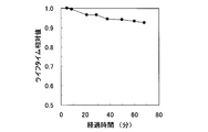
- FIG. 2 is a graph showing a relationship between an elapsed time after chemical passivation treatment in Example 1 and a recombination lifetime relative value.
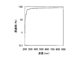
- 3 is a graph showing the relationship between the wavelength of light and the transmittance of a polyethylene bag in Example 1.
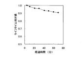
- FIG. 6 is a graph showing the relationship between the elapsed time after chemical passivation treatment in Example 2 and the recombination lifetime relative value. It is the graph which showed the relationship between the wavelength of the light of the ultraviolet-ray cut polyethylene bag in Example 2, and the transmittance
- FIG. 6 is a graph showing the relationship between the light wavelength and transmittance of a Mylar film in Example 3.
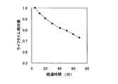
- FIG. 6 is a graph showing a relationship between an elapsed time after chemical passivation treatment and a recombination lifetime relative value in Comparative Example 1.
- 6 is a graph showing the relationship between the elapsed time after chemical passivation treatment and the recombination lifetime relative value in Comparative Example 2.
- 6 is a graph showing the relationship between light wavelength and transmittance of a polyethylene terephthalate bag in Comparative Example 2. It is the graph which showed the relationship between the elapsed time after the chemical passivation process in Example 4, and a recombination lifetime relative value. It is the graph which showed the relationship between the elapsed time after the chemical passivation process in the comparative example 3, and a recombination lifetime relative value.
- the present inventor has found that light has an influence on the speed of the chemical reaction, and the chemical reaction is suppressed by shielding the light, so that the change with time is reduced. Furthermore, the present inventors have found that the change with time can be reduced to the same extent as in the case of light shielding by cutting ultraviolet rays having a short wavelength among light.
- a silicon substrate to be evaluated is prepared.
- the method for preparing the silicon substrate is not particularly limited in the present invention.
- it can be prepared by cutting the wafer from the silicon single crystal and performing chemical etching to remove the cutting damage.
- the silicon substrate to be evaluated can be prepared by growing the epitaxial layer in the epitaxial growth furnace.
- the natural oxide film is removed with a hydrofluoric acid aqueous solution before the chemical passivation treatment.
- chemical passivation treatment is performed to suppress surface recombination of the silicon substrate in an environment where the silicon substrate is protected from ultraviolet rays.
- the chemical passivation treatment can be performed using an iodine alcohol solution.
- an iodine ethanol solution can be used.
- the recombination lifetime is measured in an environment where the chemically passivated silicon substrate is protected from ultraviolet rays.
- a microwave photoconductive decay method ⁇ -PCD method
- the measurement conditions in the ⁇ -PCD method may be those generally used. For example, measurement can be performed under the conditions described in Non-Patent Document 1.
- a commercially available measuring apparatus can be used.
- the measurement of the recombination lifetime from the chemical passivation treatment can be performed in a light-shielded environment.
- a light-shielded environment for example, the entire room may be shielded, or only the work area may be shielded.
- the measurement of the recombination lifetime from the chemical passivation treatment can be performed in an environment where the ultraviolet rays are cut.
- an environment in which the ultraviolet rays are cut for example, a yellow room can be used. Work is extremely difficult in a light-shielded environment, but work is easier in an environment where ultraviolet rays are cut off.
- the silicon substrate is accommodated in a synthetic resin bag or container made of a material that cuts ultraviolet rays, and a chemical passivation treatment is performed by injecting a solution for chemical passivation and recombination. Lifetime can be measured.
- Polyethylene or polypropylene can be used as the synthetic resin.
- Example 1 By the Czochralski method, a silicon single crystal ingot having a p-type conductivity, a resistivity of about 10 ⁇ ⁇ cm, and an oxygen concentration of about 15 ppma (JEITA) was grown. The diameter is 200 mm, and the crystal axis orientation is ⁇ 100>. And from the silicon single crystal ingot, a silicon substrate having a mirror polished finish was produced by a standard wafer processing process.
- the wavelength of the pulse laser for carrier excitation was 904 nm, the pulse width was 200 ns, the carrier injection amount was 1.2E13 / cm 2 , and the microwave frequency was about 10 GHz.
- the measurement was repeatedly performed at arbitrary time intervals.
- the silicon substrate was held in a light-shielded device between repeated measurements.
- the light transmittance of the transparent polyethylene bag was measured with a spectrophotometer (Hitachi spectrophotometer U-3000).
- the measurement result of the recombination lifetime is shown in FIG.
- the horizontal axis represents the elapsed time after the chemical passivation treatment
- the vertical axis represents the relative value of the measured value when the first recombination lifetime measured value is 1.
- the absolute value of the first measured value is about 1800 ⁇ sec, and the same applies to Examples 2 and 3 and Comparative Examples 1 and 2 described later.
- the measurement result of the light transmittance was shown in FIG. In the graph of FIG. 2, the horizontal axis indicates the wavelength of light, and the vertical axis indicates the light transmittance.
- the decrease in the measured value after 60 minutes from the chemical passivation treatment was within 10%.
- the transparent polyethylene bag used in this example has a light transmittance of several tens of percent at a wavelength of about 400 nm or less, and the UV-cut polyethylene bag used in Example 2 described later. It was higher than that. From this result, it can be seen that by measuring the recombination lifetime from chemical passivation in an environment shielded from light, the change with time can be made smaller than in the case of the comparative example described later.
- Example 2 A silicon substrate prepared from the same silicon single crystal ingot as in Example 1 was prepared.
- the recombination lifetime was measured by the ⁇ -PCD method in a light-shielded apparatus.
- the measurement conditions for the recombination lifetime are the same as in Example 1.
- the measurement was repeatedly performed at arbitrary time intervals. During the chemical passivation treatment and between repeated measurements, it was placed under a fluorescent lamp of about 400 lx. Moreover, the light transmittance of the said ultraviolet cut polyethylene bag was measured with the spectrophotometer.
- the measurement result of the recombination lifetime is shown in FIG.
- the horizontal axis represents the elapsed time after the chemical passivation treatment
- the vertical axis represents the relative value of the measured value when the first recombination lifetime measured value is 1.
- the measurement result of the light transmittance was shown in FIG.
- the horizontal axis indicates the wavelength of light
- the vertical axis indicates the light transmittance.
- the decrease in the measured value after 60 minutes from the chemical passivation treatment was within 10%.
- the ultraviolet light cut polyethylene bag used in this example had a light transmittance of 0.1% or less at a wavelength of about 400 nm or less.
- Example 3 A silicon substrate prepared from the same silicon single crystal ingot as in Example 1 was prepared.
- Example 2 After removing the natural oxide film of the prepared silicon substrate with a hydrofluoric acid aqueous solution, it is housed in a transparent polyethylene bag having the same high ultraviolet transmittance as in Example 1, and the polyethylene bag is made of Mylar film (translucent yellow). After covering, chemical passivation treatment was performed by injecting iodine ethanol solution. Thereafter, the recombination lifetime was measured by the ⁇ -PCD method in a light-shielded apparatus. The measurement conditions for the recombination lifetime are the same as in Example 1. In order to examine the change over time of the recombination lifetime measurement, the measurement was repeatedly performed at arbitrary time intervals. During the chemical passivation treatment and between repeated measurements, it was placed under a fluorescent lamp of about 400 lx. The light transmittance of the Mylar film was measured with a spectrophotometer.
- the measurement result of the recombination lifetime is shown in FIG.
- the horizontal axis represents the elapsed time after the chemical passivation treatment
- the vertical axis represents the relative value of the measured value when the first recombination lifetime measured value is 1.
- the measurement result of the light transmittance was shown in FIG.
- the horizontal axis indicates the wavelength of light
- the vertical axis indicates the light transmittance.
- the decrease in the measured value after 60 minutes from the chemical passivation treatment was within 10%.
- the mylar film used in this example had a light transmittance of 0.1% or less at a wavelength of about 400 nm or less. That is, the silicon substrate was protected from ultraviolet rays by covering a transparent polyethylene bag having a high ultraviolet transmittance with a Mylar film having a low ultraviolet transmittance.
- Example 1 A silicon substrate prepared from the same silicon single crystal ingot as in Example 1 was prepared.
- the measurement result of the recombination lifetime is shown in FIG.
- the horizontal axis indicates the elapsed time after the chemical passivation treatment
- the vertical axis indicates the relative value of the measured value when the first recombination lifetime measured value is 1.
- the decrease in the measured value after about 60 minutes from the chemical passivation treatment is about 25%, and it can be seen that the change with time is larger than in the case of Examples 1 to 3.
- the light transmittance of the transparent polyethylene bag used in this comparative example is shown in FIG. 2, and the light transmittance at a wavelength of about 400 nm or less is several tens of percent.
- the measurement result of the recombination lifetime is shown in FIG.
- the horizontal axis represents the elapsed time after the chemical passivation treatment
- the vertical axis represents the relative value of the measured value when the first recombination lifetime measured value is 1.
- the measurement result of the light transmittance is shown in FIG.
- the horizontal axis indicates the wavelength of light
- the vertical axis indicates the light transmittance.
- the change in the measured value after 50 minutes from the chemical passivation treatment is 50% or more, and the change with time is larger than in the case of Examples 1 to 3.
- the transparent PET bag used in this comparative example had a light transmittance of about 70% at a wavelength of about 400 nm or less, which was higher than that of Comparative Example 1. From this result, it can be seen that the change with time increases as the light transmittance at a wavelength of about 400 nm or less increases.
- Example 4 By the Czochralski method, a silicon single crystal ingot having a conductivity type of p-type, a resistivity of about 60 ⁇ ⁇ cm, and an oxygen concentration of about 10 ppma (JEITA) was grown. The diameter is 200 mm, and the crystal axis orientation is ⁇ 100>. And from the silicon single crystal ingot, a silicon substrate having a mirror polished finish was produced by a standard wafer processing process.
- JEITA oxygen concentration
- Example 2 After removing the natural oxide film of the prepared silicon substrate with a hydrofluoric acid aqueous solution, it was housed in the same ultraviolet cut polyethylene bag as in Example 2, and an iodine ethanol solution was injected to perform chemical passivation treatment. Thereafter, the recombination lifetime was measured by the ⁇ -PCD method in a light-shielded apparatus.
- the measurement conditions for the recombination lifetime are the same as in Example 1. In order to examine the change over time of the recombination lifetime measurement, the measurement was repeatedly performed at arbitrary time intervals. During the chemical passivation treatment and between repeated measurements, it was placed under a fluorescent lamp of about 400 lx.
- the measurement result of the recombination lifetime is shown in FIG.
- the horizontal axis represents the elapsed time after the chemical passivation treatment
- the vertical axis represents the relative value of the measured value when the first recombination lifetime measured value is 1.
- the absolute value of the first measured value is about 4200 ⁇ sec, and the same applies to Comparative Example 3 described later.
- the measurement result of the recombination lifetime is shown in FIG.
- the horizontal axis represents the elapsed time after the chemical passivation treatment
- the vertical axis represents the relative value of the measured value when the first recombination lifetime measured value is 1.
- the decrease in the measured value after about 60 minutes from the chemical passivation treatment is about 10%, which indicates that the change with time is larger than that in Example 4.
- the light transmittance of the transparent polyethylene bag used in this comparative example is shown in FIG. 2, and the light transmittance at a wavelength of about 400 nm or less is several tens of percent.
- the present invention is not limited to the above embodiment.
- the above-described embodiment is an exemplification, and the present invention has substantially the same configuration as the technical idea described in the claims of the present invention, and any device that exhibits the same function and effect is the present invention. It is included in the technical scope of the invention.
Landscapes
- Physics & Mathematics (AREA)
- General Physics & Mathematics (AREA)
- Testing Or Measuring Of Semiconductors Or The Like (AREA)
- Investigating, Analyzing Materials By Fluorescence Or Luminescence (AREA)
Abstract
Description
チョクラルスキー法により、導電型がp型で、抵抗率が約10Ω・cm、酸素濃度が約15ppma(JEITA)のシリコン単結晶インゴットを育成した。直径は200mm、結晶軸方位は<100>である。そして、そのシリコン単結晶インゴットから、標準的なウェーハ加工プロセスにより、鏡面研磨仕上げのシリコン基板を作製した。
実施例1と同じシリコン単結晶インゴットから作製されたシリコン基板を準備した。
実施例1と同じシリコン単結晶インゴットから作製されたシリコン基板を準備した。
実施例1と同じシリコン単結晶インゴットから作製されたシリコン基板を準備した。
実施例1と同じシリコン単結晶インゴットから作製されたシリコン基板を準備した。
チョクラルスキー法により、導電型がp型で、抵抗率が約60Ω・cm、酸素濃度が約10ppma(JEITA)のシリコン単結晶インゴットを育成した。直径は200mm、結晶軸方位は<100>である。そして、そのシリコン単結晶インゴットから、標準的なウェーハ加工プロセスにより、鏡面研磨仕上げのシリコン基板を作製した。
実施例4と同じシリコン単結晶インゴットから作製されたシリコン基板を準備した。
Claims (6)
- シリコン基板の表面に対してケミカルパシベーション処理を行った後に、再結合ライフタイムを測定する方法であって、
前記ケミカルパシベーション処理から前記再結合ライフタイムの測定が完了するまでの間、少なくとも前記シリコン基板を紫外線から防護する紫外線防護処理が行われることを特徴とするシリコン基板の再結合ライフタイム測定方法。 - 前記ケミカルパシベーション処理から前記再結合ライフタイムの測定を、遮光された環境下で行うことで、前記紫外線防護処理が行われることを特徴とする請求項1に記載のシリコン基板の再結合ライフタイム測定方法。
- 前記ケミカルパシベーション処理から前記再結合ライフタイムの測定を、紫外線がカットされた環境下で行うことで、前記紫外線防護処理が行われることを特徴とする請求項1に記載のシリコン基板の再結合ライフタイム測定方法。
- 前記ケミカルパシベーション処理は、前記シリコン基板を紫外線をカットする材質の合成樹脂製の袋あるいは容器に挿入してケミカルパシベーション用の溶液に浸漬させることにより行い、再結合ライフタイムを測定することを特徴とする請求項1~請求項3のいずれか一項に記載のシリコン基板の再結合ライフタイム測定方法。
- 前記ケミカルパシベーション処理を、ヨウ素アルコール溶液を用いて行うことを特徴とする請求項1~請求項4のいずれか一項に記載のシリコン基板の再結合ライフタイム測定方法。
- 前記再結合ライフタイムの測定は、マイクロ波光導電減衰法により測定することを特徴とする請求項1~請求項5のいずれか一項に記載のシリコン基板の再結合ライフタイム測定方法。
Priority Applications (4)
| Application Number | Priority Date | Filing Date | Title |
|---|---|---|---|
| KR1020157015734A KR102038325B1 (ko) | 2013-02-15 | 2013-12-27 | 실리콘 기판의 재결합 라이프타임 측정 방법 |
| CN201380068161.8A CN104871302B (zh) | 2013-02-15 | 2013-12-27 | 硅基板的再结合寿命测定方法 |
| DE112013006678.5T DE112013006678T5 (de) | 2013-02-15 | 2013-12-27 | Verfahren zur Messung der Rekombinationslebensdauer eines Siliziumsubstrats |
| US14/764,856 US9530702B2 (en) | 2013-02-15 | 2013-12-27 | Method for measuring recombination lifetime of silicon substrate |
Applications Claiming Priority (2)
| Application Number | Priority Date | Filing Date | Title |
|---|---|---|---|
| JP2013-027242 | 2013-02-15 | ||
| JP2013027242A JP6080101B2 (ja) | 2013-02-15 | 2013-02-15 | シリコン基板の再結合ライフタイム測定方法 |
Publications (1)
| Publication Number | Publication Date |
|---|---|
| WO2014125751A1 true WO2014125751A1 (ja) | 2014-08-21 |
Family
ID=51353770
Family Applications (1)
| Application Number | Title | Priority Date | Filing Date |
|---|---|---|---|
| PCT/JP2013/085065 Ceased WO2014125751A1 (ja) | 2013-02-15 | 2013-12-27 | シリコン基板の再結合ライフタイム測定方法 |
Country Status (7)
| Country | Link |
|---|---|
| US (1) | US9530702B2 (ja) |
| JP (1) | JP6080101B2 (ja) |
| KR (1) | KR102038325B1 (ja) |
| CN (1) | CN104871302B (ja) |
| DE (1) | DE112013006678T5 (ja) |
| TW (1) | TWI525729B (ja) |
| WO (1) | WO2014125751A1 (ja) |
Families Citing this family (4)
| Publication number | Priority date | Publication date | Assignee | Title |
|---|---|---|---|---|
| KR20180091246A (ko) | 2017-02-06 | 2018-08-16 | 에스케이실트론 주식회사 | 웨이퍼 제조 방법 |
| JP7185879B2 (ja) * | 2019-08-30 | 2022-12-08 | 株式会社Sumco | 半導体試料の評価方法 |
| JP7249395B1 (ja) * | 2021-11-10 | 2023-03-30 | 株式会社Sumco | 半導体試料の評価方法、半導体試料の評価装置および半導体ウェーハの製造方法 |
| CN115166460B (zh) * | 2022-06-29 | 2025-09-05 | 泰州中来光电科技有限公司 | 一种测试晶体硅体区复合的方法 |
Citations (2)
| Publication number | Priority date | Publication date | Assignee | Title |
|---|---|---|---|---|
| JPH08335618A (ja) * | 1995-06-06 | 1996-12-17 | Kobe Steel Ltd | 半導体試料のキャリアのライフタイム測定方法及びその装置 |
| JP2007048959A (ja) * | 2005-08-10 | 2007-02-22 | Toshiba Ceramics Co Ltd | シリコンウェーハのライフタイム測定方法 |
Family Cites Families (8)
| Publication number | Priority date | Publication date | Assignee | Title |
|---|---|---|---|---|
| US5327195A (en) * | 1993-03-31 | 1994-07-05 | Fotodyne Incorporated | Transilluminator |
| JP3665232B2 (ja) * | 1998-10-09 | 2005-06-29 | 株式会社神戸製鋼所 | シリコン半導体の鉄濃度評価方法及びその装置 |
| JP3496058B2 (ja) * | 2001-05-01 | 2004-02-09 | 独立行政法人産業技術総合研究所 | 半導体基板の表面不活性化方法及び半導体基板 |
| JP3778432B2 (ja) * | 2002-01-23 | 2006-05-24 | 東京エレクトロン株式会社 | 基板処理方法および装置、半導体装置の製造装置 |
| JP2006351594A (ja) | 2005-06-13 | 2006-12-28 | Toshiba Ceramics Co Ltd | 半導体ウェーハの電気特性の測定方法 |
| EP2037288B1 (en) * | 2007-09-11 | 2011-06-22 | S.O.I. TEC Silicon on Insulator Technologies | Volume lifetime measurement |
| JP5455393B2 (ja) * | 2009-02-20 | 2014-03-26 | Sumco Techxiv株式会社 | 半導体ウエハの再結合ライフタイム測定方法 |
| WO2011163510A2 (en) * | 2010-06-23 | 2011-12-29 | California Institute Of Technology | Atomic layer deposition of chemical passivation layers and high performance anti-reflection coatings on back-illuminated detectors |
-
2013
- 2013-02-15 JP JP2013027242A patent/JP6080101B2/ja active Active
- 2013-12-27 KR KR1020157015734A patent/KR102038325B1/ko active Active
- 2013-12-27 WO PCT/JP2013/085065 patent/WO2014125751A1/ja not_active Ceased
- 2013-12-27 DE DE112013006678.5T patent/DE112013006678T5/de not_active Ceased
- 2013-12-27 US US14/764,856 patent/US9530702B2/en active Active
- 2013-12-27 CN CN201380068161.8A patent/CN104871302B/zh active Active
-
2014
- 2014-01-15 TW TW103101422A patent/TWI525729B/zh active
Patent Citations (2)
| Publication number | Priority date | Publication date | Assignee | Title |
|---|---|---|---|---|
| JPH08335618A (ja) * | 1995-06-06 | 1996-12-17 | Kobe Steel Ltd | 半導体試料のキャリアのライフタイム測定方法及びその装置 |
| JP2007048959A (ja) * | 2005-08-10 | 2007-02-22 | Toshiba Ceramics Co Ltd | シリコンウェーハのライフタイム測定方法 |
Also Published As
| Publication number | Publication date |
|---|---|
| CN104871302B (zh) | 2019-04-05 |
| JP6080101B2 (ja) | 2017-02-15 |
| KR102038325B1 (ko) | 2019-10-30 |
| TW201436077A (zh) | 2014-09-16 |
| CN104871302A (zh) | 2015-08-26 |
| US9530702B2 (en) | 2016-12-27 |
| US20160005664A1 (en) | 2016-01-07 |
| DE112013006678T5 (de) | 2015-10-29 |
| KR20150117249A (ko) | 2015-10-19 |
| TWI525729B (zh) | 2016-03-11 |
| JP2014157889A (ja) | 2014-08-28 |
Similar Documents
| Publication | Publication Date | Title |
|---|---|---|
| JP6080101B2 (ja) | シリコン基板の再結合ライフタイム測定方法 | |
| JP5024865B2 (ja) | 半導体基板の評価方法 | |
| US8411263B2 (en) | Method of evaluating silicon wafer and method of manufacturing silicon wafer | |
| US8481346B2 (en) | Method of analyzing iron concentration of boron-doped P-type silicon wafer and method of manufacturing silicon wafer | |
| WO2018216203A1 (ja) | GaAs基板およびその製造方法 | |
| KR20180010187A (ko) | 실리콘 에피택셜 웨이퍼의 제조방법 및 평가방법 | |
| JP5467923B2 (ja) | 金属汚染評価用シリコンウエーハの製造方法 | |
| CN101140868B (zh) | 外延晶片及其制造方法 | |
| JP2009302240A (ja) | 再結合ライフタイム評価の前処理方法 | |
| JP5590002B2 (ja) | 金属汚染評価方法及びエピタキシャルウェーハの製造方法 | |
| KR101858447B1 (ko) | 결정 결함의 검출방법 | |
| JP5742761B2 (ja) | 金属汚染検出方法及びそれを用いたシリコンエピタキシャルウェーハの製造方法 | |
| JP5742742B2 (ja) | 金属汚染評価方法 | |
| JP6817545B2 (ja) | シリコン中の炭素測定方法 | |
| JP2013161821A (ja) | 金属汚染評価用シリコン基板の選別方法 | |
| JP5471780B2 (ja) | ボロンドープp型シリコン中の鉄濃度測定方法およびボロンドープp型シリコンウェーハの製造方法 | |
| JPWO2008023639A1 (ja) | エピタキシャル成長用半導体基板及びその製造方法 | |
| JP5621733B2 (ja) | シリコン基板の再結合ライフタイムの測定方法 | |
| JP5373364B2 (ja) | シリコンウェーハのキャリアライフタイム測定方法 | |
| JP2985583B2 (ja) | シリコンウエーハの鏡面加工表面における加工変質層検査方法とその厚さ測定方法 | |
| JP5828307B2 (ja) | シリコン基板の再結合ライフタイム測定の前処理方法 | |
| Yan et al. | On the mechanism of luminescence from porous silicon nanostructures | |
| Takahashi et al. | Three-dimensional imaging of threading dislocations in GaN by multimodal stimulated Raman scattering microscopy | |
| KR101589601B1 (ko) | 웨이퍼 제조 방법 | |
| JP2002110687A (ja) | シリコン半導体基板 |
Legal Events
| Date | Code | Title | Description |
|---|---|---|---|
| 121 | Ep: the epo has been informed by wipo that ep was designated in this application |
Ref document number: 13875088 Country of ref document: EP Kind code of ref document: A1 |
|
| ENP | Entry into the national phase |
Ref document number: 20157015734 Country of ref document: KR Kind code of ref document: A |
|
| WWE | Wipo information: entry into national phase |
Ref document number: 14764856 Country of ref document: US |
|
| WWE | Wipo information: entry into national phase |
Ref document number: 1120130066785 Country of ref document: DE Ref document number: 112013006678 Country of ref document: DE |
|
| 122 | Ep: pct application non-entry in european phase |
Ref document number: 13875088 Country of ref document: EP Kind code of ref document: A1 |