WO2014112385A1 - コンデンサおよびその製造方法 - Google Patents
コンデンサおよびその製造方法 Download PDFInfo
- Publication number
- WO2014112385A1 WO2014112385A1 PCT/JP2014/000214 JP2014000214W WO2014112385A1 WO 2014112385 A1 WO2014112385 A1 WO 2014112385A1 JP 2014000214 W JP2014000214 W JP 2014000214W WO 2014112385 A1 WO2014112385 A1 WO 2014112385A1
- Authority
- WO
- WIPO (PCT)
- Prior art keywords
- lead terminal
- capacitor
- resin layer
- lead
- bending
- Prior art date
- Legal status (The legal status is an assumption and is not a legal conclusion. Google has not performed a legal analysis and makes no representation as to the accuracy of the status listed.)
- Ceased
Links
Images



Classifications
-
- H—ELECTRICITY
- H01—ELECTRIC ELEMENTS
- H01G—CAPACITORS; CAPACITORS, RECTIFIERS, DETECTORS, SWITCHING DEVICES, LIGHT-SENSITIVE OR TEMPERATURE-SENSITIVE DEVICES OF THE ELECTROLYTIC TYPE
- H01G9/00—Electrolytic capacitors, rectifiers, detectors, switching devices, light-sensitive or temperature-sensitive devices; Processes of their manufacture
- H01G9/004—Details
- H01G9/008—Terminals
- H01G9/012—Terminals specially adapted for solid capacitors
-
- H—ELECTRICITY
- H01—ELECTRIC ELEMENTS
- H01G—CAPACITORS; CAPACITORS, RECTIFIERS, DETECTORS, SWITCHING DEVICES, LIGHT-SENSITIVE OR TEMPERATURE-SENSITIVE DEVICES OF THE ELECTROLYTIC TYPE
- H01G2/00—Details of capacitors not covered by a single one of groups H01G4/00-H01G11/00
- H01G2/02—Mountings
- H01G2/06—Mountings specially adapted for mounting on a printed-circuit support
- H01G2/065—Mountings specially adapted for mounting on a printed-circuit support for surface mounting, e.g. chip capacitors
-
- H—ELECTRICITY
- H01—ELECTRIC ELEMENTS
- H01G—CAPACITORS; CAPACITORS, RECTIFIERS, DETECTORS, SWITCHING DEVICES, LIGHT-SENSITIVE OR TEMPERATURE-SENSITIVE DEVICES OF THE ELECTROLYTIC TYPE
- H01G9/00—Electrolytic capacitors, rectifiers, detectors, switching devices, light-sensitive or temperature-sensitive devices; Processes of their manufacture
- H01G9/0029—Processes of manufacture
-
- H—ELECTRICITY
- H01—ELECTRIC ELEMENTS
- H01G—CAPACITORS; CAPACITORS, RECTIFIERS, DETECTORS, SWITCHING DEVICES, LIGHT-SENSITIVE OR TEMPERATURE-SENSITIVE DEVICES OF THE ELECTROLYTIC TYPE
- H01G9/00—Electrolytic capacitors, rectifiers, detectors, switching devices, light-sensitive or temperature-sensitive devices; Processes of their manufacture
- H01G9/004—Details
- H01G9/08—Housing; Encapsulation
-
- H—ELECTRICITY
- H01—ELECTRIC ELEMENTS
- H01G—CAPACITORS; CAPACITORS, RECTIFIERS, DETECTORS, SWITCHING DEVICES, LIGHT-SENSITIVE OR TEMPERATURE-SENSITIVE DEVICES OF THE ELECTROLYTIC TYPE
- H01G9/00—Electrolytic capacitors, rectifiers, detectors, switching devices, light-sensitive or temperature-sensitive devices; Processes of their manufacture
- H01G9/004—Details
- H01G9/08—Housing; Encapsulation
- H01G9/10—Sealing, e.g. of lead-in wires
-
- H—ELECTRICITY
- H01—ELECTRIC ELEMENTS
- H01G—CAPACITORS; CAPACITORS, RECTIFIERS, DETECTORS, SWITCHING DEVICES, LIGHT-SENSITIVE OR TEMPERATURE-SENSITIVE DEVICES OF THE ELECTROLYTIC TYPE
- H01G9/00—Electrolytic capacitors, rectifiers, detectors, switching devices, light-sensitive or temperature-sensitive devices; Processes of their manufacture
- H01G9/15—Solid electrolytic capacitors
-
- Y—GENERAL TAGGING OF NEW TECHNOLOGICAL DEVELOPMENTS; GENERAL TAGGING OF CROSS-SECTIONAL TECHNOLOGIES SPANNING OVER SEVERAL SECTIONS OF THE IPC; TECHNICAL SUBJECTS COVERED BY FORMER USPC CROSS-REFERENCE ART COLLECTIONS [XRACs] AND DIGESTS
- Y10—TECHNICAL SUBJECTS COVERED BY FORMER USPC
- Y10T—TECHNICAL SUBJECTS COVERED BY FORMER US CLASSIFICATION
- Y10T29/00—Metal working
- Y10T29/42—Piezoelectric device making
Definitions
- the present invention relates to a capacitor such as a solid electrolytic capacitor in which an exterior member is formed of a resin mold, and a manufacturing method thereof.
- the lead terminals of the capacitor elements are drawn from the resin layer.
- the lead terminal is bent along the resin layer surface and processed into a face bonding terminal.
- This type of capacitor is required to have a low profile that suppresses the height. With a low-profile capacitor, the height on the mounting substrate can be lowered, which contributes to the reduction in size and weight of the mounted device.
- JP 2000-021683 A Japanese Patent Laid-Open No. 2003-272966
- the lead terminal used for connection to the substrate by face bonding is processed to be bent along the resin layer.
- the lead terminal has elasticity due to the material, and even if it is bent along the resin layer, bending back (springback) occurs due to the elasticity.
- the mounting surface of the capacitor is not parallel to the mounting substrate, and the mounting stability of the capacitor is lacking.
- a notch is formed in the lead terminal, and the bending position of the lead terminal is determined by the notch, and elasticity is reduced to prevent bending back.
- the mounting stability of the capacitor on the mounting board is improved by flattening the board mounting surface of the lead terminal.
- the lead terminal led out from the resin layer is subjected to bending processing through flat processing and notch formation.
- FIG. 6 shows an example of the lead terminal processing step.
- This processing step includes, for example, a lead terminal flattening step, a notch forming step, and a bending step.
- the lead terminal 104 drawn out from the resin layer 102 covering the capacitor element 100 is sandwiched between the mold 106-1 and the mold 106-2. Then, it is molded by applying pressure in the direction of the arrow.
- the pressing surface of the mold 106-1 is a flat surface, whereas the convex portion 108 and the flat surface 110 are formed on the mold 106-2.
- the lead terminal 104 is formed with a notch 112 and a flat surface 114 from the resin layer 102 side. When the notches 112 and the flat surface 114 are formed, the lead terminal 104 has an extended portion 116 near the resin layer 102.
- the lead terminal 104 is bent at the notch 112, and the notch 112 is bent inward.
- the corner portion 120 facing the notch 112 hits the stepped portion 118 generated by the formation of the notch 112, and the lead terminal 104 is prevented from being bent. For this reason, the lead terminal 104 cannot be bent flat even if the notch 112 is formed.
- an object of the present invention is to provide a capacitor that prevents a lead terminal from being bent back and realizes a flattening process, and a method for manufacturing the same.
- a capacitor of the present invention is a capacitor in which a capacitor element to which a lead terminal is connected is coated with a resin, and the resin layer is connected to the lead terminal derived from the resin layer covering the capacitor element. It is provided with a gap portion exposed from the outer surface, a thin portion, and a step portion that is a boundary portion between the gap portion and the thin portion, and is arranged on the resin layer side by bending the thin portion toward the step portion.
- the lead terminal is arranged so that the stepped portion and the thin portion overlap each other, and the thin portion surrounds the interval portion.
- the height of the stepped portion may be set smaller than the width of the thin portion.
- a protrusion is formed on the side surface portion of the lead terminal or the outer surface side of the resin layer from which the lead terminal is led out, and the outer surface of the resin layer is formed by bending the lead terminal.
- the protruding portion of the lead terminal may be disposed in the vicinity of the portion, or the lead terminal may be disposed in the vicinity of the protruding portion formed in the resin layer facing the lead terminal.
- the protruding portion of the lead terminal hits the resin surface on the outer surface side of the resin layer by bending the lead terminal, or the lead terminal hits the protruding portion of the resin layer,
- the bending angle may be limited by the protrusion of the lead terminal or the protrusion of the resin layer.
- the capacitor includes a plurality of protrusions having different heights between the terminal portion of the lead terminal and the thin portion, and among these protrusions, the height of the protrusion on the terminal side is set to other height. You may set higher than a projection part.
- a capacitor manufacturing method of the present invention is a capacitor manufacturing method in which a capacitor element to which a lead terminal is connected is coated with a resin, wherein the lead terminal is derived from a resin layer covering the capacitor element.
- a gap portion exposed from the outer surface of the resin layer is set, a step portion is provided between the gap portion and a thin portion is formed in the lead terminal, and the lead is formed toward the step portion by the thin portion.
- the process includes bending the terminal so that the stepped portion and the thin portion overlap, and the thin portion surrounds the spacing portion.
- the above-described capacitor manufacturing method may preferably include a process of forming the stepped portion with a height smaller than the thin portion.
- the resin is further formed by forming a protrusion on a side surface portion of the lead terminal or an outer surface side of the resin layer from which the lead terminal is led, and bending the lead terminal.
- a process of disposing the protrusion of the lead terminal in the vicinity of the outer surface of the layer or disposing the lead terminal in the vicinity of the protrusion formed on the resin layer facing the lead terminal may be included.
- the protrusion of the lead terminal hits the resin surface on the outer surface side of the resin layer by bending the lead terminal, or the lead terminal hits the protrusion of the resin layer,
- a process of limiting the bending angle of the lead terminal by the protruding portion of the lead terminal or the protruding portion of the resin layer may be included.
- the lead terminal bending position can be kept constant, bending back can be prevented, and lead terminal bending accuracy can be improved.
- FIG. 1A shows a part of the capacitor according to the first embodiment.
- the configuration shown in FIG. 1A is an example, and the present invention is not limited to such a configuration.
- the capacitor 2 is, for example, a solid electrolytic capacitor and is an example of the capacitor of the present invention.
- a capacitor element 4 wound in a cylindrical shape is used.
- this capacitor element 4 as an example, an anode-side electrode foil, a first separator, a cathode-side electrode foil, and a second separator are laminated, wound into a cylindrical shape, and then impregnated with an electrolyte.
- the capacitor element 4 has an anode-side electrode terminal connected to the anode-side electrode foil and a cathode-side electrode terminal connected to the cathode-side electrode foil.
- These lead terminals are drawn out from the element end face 6 of the capacitor element 4.
- the illustrated lead terminal 8 may be either an anode side or cathode side lead terminal.
- the capacitor element 4 is resin-molded with an insulating resin and covered with a resin layer 10.
- the lead terminal 8 drawn from the capacitor element 4 is drawn through the resin layer 10.
- the extended portion 12, the notch 14 and the flat portion 16 are formed on the lead terminal 8 by molding using a mold.
- the elongated portion 12 is an elongated portion generated in the lead terminal 8 by the molding process, and is generated at a boundary portion with the resin layer 10.
- the extending portion 12 is an example of a space portion between the resin layer 10 and the notch 14 and is a rod-shaped portion having the same diameter.
- the notch part 14 is an example of a thin part.
- the notch 14 is an example of a thin portion formed in the lead terminal 8.
- the notch 14 includes a first stepped portion 18-1 between the extended portion 12 and a second stepped portion 18-2 between the flat portion 16.
- Each of the step portions 18-1 and 18-2 includes a standing wall surface formed in a direction orthogonal to or intersecting with the central axis O of the lead terminal 8, for example.
- the width b is set to a relationship of a ⁇ b with respect to the height a. That is, the width b is set larger than the height a.
- FIG. 1B shows the lead terminal 8 bent at the corner between the step 18-1 and the notch 14.
- a bent portion 20 is formed, so that the notch 14 is superimposed on the stepped portion 18-1, and the lead terminal 8 is connected to the resin layer 10
- the lead terminal lead-out surface 22 can be arranged in parallel.
- the bent portion 20 is set at, for example, a part of the notch 14 or a boundary portion between the notch 14 and the stepped portion 18-1, and is formed in a “V” shape having both the notch 14 and the stepped portion 18-1 as both sides.
- the width b of the notch 14 is larger than the height a of the stepped portion 18-1, the stepped portion 18-2 of the notch 14 is disposed beyond the wall surface of the lead terminal 8, and the stepped portion 18-2 of the notch 14 is disposed.
- the side surface of the extended portion 12 is connected to the step portion 18-2. Parallel state.
- the bending accuracy of the lead terminal 8 can be improved by specifying the bending position of the lead terminal 8 to the V-shaped bent portion 20 where the step portion 18-1 and the notch 14 intersect.
- the lead terminal 8 can be bent to a position parallel to the lead terminal lead surface 22 of the resin layer 10 without causing a springback. According to the capacitor 2 provided with such lead terminals 8, it is possible to stabilize the placement accuracy with respect to the mounting substrate.
- the height of the capacitor 2 can be made constant, which contributes to a reduction in height.
- FIG. 2A shows the capacitor 2 according to the second embodiment.
- the same parts as those in FIG. 2A are identical.
- the extending portion 12 has a rod shape with the same diameter, whereas in the second embodiment, a hemispherical curved portion is provided. For this reason, the stepped portion 18-1 is formed of a curved surface portion.
- the lead terminal 8 has no stepped portion 18-1 with a corner and is a curved surface portion. Therefore, as shown in FIG.
- the bent portion 20 is formed by bending the lead terminal 8 with the corner portion, which is the boundary portion, as the bending start point. At the time of this bending, the stepped portion 18-1 is deformed along with the formation of the bent portion 20, so that it escapes from the stepped portion 18-2, and interference between the two can be avoided.
- the height a of the stepped portion 18-1 and the width b of the notch 14 can be set in a relationship of a ⁇ b, and the width b of the notch 14 can be reduced.
- the lead terminal 8 can be bent at the corner formed by the notch 14 and the stepped portion 18-1, and the spring back of the lead terminal 8 is avoided. be able to.
- the lead terminal 8 can be bent with the corner formed by the notch 14 which is a narrow thin part and the stepped portion 18-1 made of a curved surface as a starting point of bending, and the spring back of the lead terminal 8 is avoided.
- the lead terminal 8 can be bent parallel to the lead terminal lead surface 22 of the resin layer 10. Thereby, similarly to the first embodiment, the bending accuracy of the lead terminal 8 can be increased.
- the height of the capacitor 2 is made uniform, so that the accuracy of the fixed position of the capacitor 2 with respect to the mounting surface of the mounting board can be improved.
- FIG. 3A shows a cross section of the solid electrolytic capacitor.
- the configuration illustrated in FIG. 3A is an example, and the present invention is not limited to such a configuration.
- the lead terminal does not become parallel to the outer surface of the resin layer depending on the length of the stretched portion even if it is bent along the outer surface of the resin layer because the length of the stretched portion generated during the flattening process is not uniform. There could be variations in the height of the capacitors.
- the lead terminal when the lead terminal is flattened in order to ensure the stability of the substrate arrangement, the lead terminal can be flattened at a desired location, while the lead terminal is between the flat surface and the lead-out portion from the resin surface. Elongation occurs.
- the boundary between the extended portion and the flat surface is the bending position. Since the length of the extended portion is not uniform, the bending position also varies. When the extended portion is long and the position away from the resin surface is the bending position, the bending angle of the lead terminal tends to be more acute, and the stability of the substrate arrangement of the lead terminal may be impaired.
- the capacitor according to this embodiment includes means for limiting the bending angle of the lead terminal regardless of the length of the extended portion caused by bending the lead terminal.
- a solid electrolytic capacitor 30 (hereinafter, simply referred to as “capacitor 30”) shown in FIG. 3A is an example of the capacitor of the present invention.
- the capacitor 30 is a capacitor element 4 wound in a cylindrical shape.
- An anode-side lead terminal 32-1 is connected to the anode-side electrode foil of the capacitor element 4, and a cathode-side lead terminal 32-2 is connected to the cathode-side electrode foil. These lead terminals 32-1 and 32-2 are drawn out from the element end face 6 of the capacitor element 4.
- the capacitor element 4 is resin-molded with a resin layer 10 as an exterior resin made of an insulating resin. That is, the outer surface of the capacitor element 4 is covered with the resin layer 10 and sealed in the resin layer 10. Therefore, the lead terminals 32-1 and 32-2 on the element end face 6 of the capacitor element 4 are drawn out through the resin layer 10.
- the resin layer 10 is in close contact with the wall surfaces of the lead terminals 32-1 and 32-2.
- the state shown in FIG. 3A is a state before the lead terminals 32-1 and 32-2 are bent, and is in a state perpendicular to the lead terminal lead surface 22 of the resin layer 10.
- the lead terminal 32-1 is formed of, for example, a cylindrical wire.
- the lead terminal 32-1 is formed with a lead terminal main body 34, an extending portion 36, a notch portion 38, and a protruding portion 40.
- a lead terminal body 34 penetrates into the layer of the resin layer 10, and an extended portion 36, a notch portion 38, and a protruding portion 40 are provided between the base side exposed from the resin layer 10 and the tip portion. Is provided.
- the notch 38 and the protrusion 40 are formed on the flat surface 42 of the lead terminals 32-1 and 32-2.
- the flat surface portion 42 is an example of a flat portion, for example, and is a portion that is flattened by pressing a round bar-shaped lead terminal material.
- the lead terminal body 34 is held by the resin layer 10.
- the extending portion 36 is an example of a spacing portion of the present invention, and is flattened and extended in a parabolic shape from the root side of the lead terminal 32-1 toward the tip portion.
- the extending portion 36 is formed, for example, when the notch portion 38 is formed on the lead terminal 32-1 by pressure molding.
- the notch portion 38 is a flat portion formed by pressure molding with respect to the lead terminal 32-1, and is an example of a thin portion of the present invention.
- the notch portion 38 is formed with a first notch portion 38-1 and a second notch portion 38-2.
- the notch portion 38-1 and the notch portion 38-2 are different in thickness by providing a step, and the notch portion 38-2 on the tip end side is formed thicker than the notch portion 38-1. That is, the notch 38-2 and the protrusion 40 are an example of a plurality of protrusions. Therefore, the protrusion 40 at the terminal end of the lead terminal 32-1 is a protrusion having a height different from that of the notch 38-2 as another protrusion, and constitutes a protrusion higher than the other protrusions. is doing.
- the protrusion 40 is formed on the end side of the notch portion 38-2 and forms the end portion of the lead terminal 32-1.
- the protrusion 40 is formed thicker than the notch 38-2.
- the width of the extended portion 36 is W
- the length of the notch portion 38-1 (notch portion length) is L1
- the length of the notch portion 38-2 (notch portion length) is L2
- the depth of 1 (notch depth) is T1
- the depth of notch 38-2 (notch depth) is T2
- the side of the lead terminal of the anode side lead terminal 32-1 the depth of the notch 38-1.
- the height of the protrusion 40 with respect to the notch 38-2 is T2
- the height of the protrusion 40 with respect to the notch 38-1 is T1 + T2. That is, the extended portion 36 is housed in the notched portion 38-1 that is a thin portion.
- the lead terminal 32-1 has been described, the lead terminal 32-2 is the same as the lead terminal 32-1, and therefore the description thereof is omitted.
- the protrusions 40 of the lead terminals 32-1 and 32-2 are arranged in the vicinity of the lead terminal lead-out surface 22.
- FIG. 4A shows the capacitor 30 including the bent lead terminals 32-1 and 32-2.
- Each of the lead terminals 32-1 and 32-2 is bent in the opposite direction, and is disposed in the vicinity of the lead terminal lead surface 22 of the resin layer 10 of the capacitor 30.
- FIG. 4B shows an enlarged view of the lead terminal 32-1 side shown in FIG. 4A.
- the lead terminal wire 32-1 is bent in the opposite direction to the lead terminal 32-2. This bending process is performed inside the notch 38-1.
- the extended portion 36 is deformed and enters the notch portion 38-1 side, between the notch portion 38-1 and the lead terminal lead surface 22, and between the notch portion 38-2 and the lead terminal lead surface 22.
- a space 44 is formed.
- the protrusion 40 is in close contact with the lead terminal lead surface 22, and the longitudinal center line Y of the lead terminal 32-1 is maintained parallel to the lead terminal lead surface 22. Thereby, the height H of the capacitor 30 is uniform.
- the protrusions 40 are provided on the leading end sides of the lead terminals 32-1 and 32-2, and are arranged on the lead terminal lead-out surface 22 of the resin layer 10, so that the lead can be read regardless of the width W of the extending portion 36. Jumping up due to bending of the terminals 32-1 and 32-2 can be prevented.
- the lead terminals 32-1 and 32-2 can keep the bending angle constant, and the variation in the height of the capacitor 30 can be reduced. In other words, when the width W is large, for example, the protrusion 40 is brought into contact with the lead terminal lead surface 22 side of the resin layer 10, so that the bending angle is limited.
- the width W of the extending portion 36 is increased, and even when the starting point of bending is separated from the lead terminal drawing surface 22, the bending angle of the lead terminals 32-1 and 32-2 is prevented from increasing, and the placement accuracy with respect to the circuit board is improved. Stabilize.
- a notch portion 38 or a projection 40 having different heights from the flange extending portion 36 toward the terminal ends of the lead terminals 32-1 and 32-2 is provided. If the step is formed, it is possible to prevent the lead terminals 32-1 and 32-2 from coming into contact with the lead terminal lead-out surface 22 of the resin layer 10 on the notch portion 38 side. As a result, the bent angles of the bent lead terminals 32-1 and 32-2 can be made uniform, and variations in the height of the capacitor 30 can be reduced. Further, in the case of two steps, the strength of the lead terminal can be maintained by providing a portion where the notch portion 38 is thick between the extending portion 36 and the protruding portion 40.
- the structure in which the steps having different heights are provided is a structure that prevents the lead terminals 32-1 and 32-2 from coming into contact with the lead terminal lead surface 22 on the notch portion 38 side when the lead terminal is bent.
- the thickness can be secured to maintain the strength of the lead terminals 32-1 and 32-2.
- the processing stress during processing of the lead terminals 32-1 and 32-2 is reduced. That is, by forming the notch portion 38-1 as a thin portion deeply and forming a plurality of steps, occurrence of crushing distortion can be prevented and the strength of the lead terminals 32-1 and 32-2 can be maintained.
- the thin portion formed as the notch portion 38-1 is the portion where the lead terminals 32-1 and 32-2 are the thinnest, and thus becomes the starting point during bending. Thereby, a bending position can be made into a thin part. By doing in this way, the dispersion
- FIG. 5A shows a solid electrolytic capacitor according to the fourth embodiment.
- the same parts as those in FIG. 5A the same parts as those in FIG. 5A.
- a protrusion 46 is formed on the edge side of the lead terminal lead surface 22 of the resin layer 10.
- the height of the protrusion 46 is set to be equal to the depth of the notch 38-2, which is an example of the thin part, that is, the height T2 of the protrusion 40 from the bottom of the notch 38-2. Good.
- the side wall 32-2 is disposed in the vicinity of the protrusion 46 formed on the lead terminal lead surface 22.
- part of the lead terminals 32-1 and 32-2 hits the protrusion 46, and the bending angle of the lead terminals 32-1 and 32-2 can be limited.
- This capacitor 30 has lead terminals 32-1 and 32-2 arranged on a protrusion 46 provided on the lead terminal lead-out surface 22 side on the lead-out surface of the lead terminals 32-1 and 32-2. Yes.
- the lead terminals 32-1 and 32-2 are limited in the angle at which the lead terminals 32-1 and 32-2 are bent, for example, when the flat portions come into contact with the protrusions 46.
- the lead terminals 32-1 and 32-2 can keep the bending positions of the lead terminals 32-1 and 32-2 constant regardless of the width W of the extending portion 36, and the bending height of the lead terminals 32-1 and 32-2 can be kept constant. Variations can be reduced.
- a solid electrolytic capacitor is illustrated as an example, but the capacitor of the present invention may be another capacitor such as an electrolytic capacitor.
- the present invention is a capacitor such as a solid electrolytic capacitor coated with a resin layer by a resin mold, which can improve the molding accuracy of the lead terminal, improve the positional accuracy with respect to the mounting substrate and stabilize the height of the capacitor. I can plan.
Landscapes
- Engineering & Computer Science (AREA)
- Power Engineering (AREA)
- Microelectronics & Electronic Packaging (AREA)
- Manufacturing & Machinery (AREA)
- Fixed Capacitors And Capacitor Manufacturing Machines (AREA)
Abstract
リード端子(8)を接続したコンデンサ素子(4)を樹脂で被覆したコンデンサ(2)であって、コンデンサ素子を覆う樹脂層(10)から導出されたリード端子に、樹脂層の外面から露出する間隔部(伸び部12)と、薄肉部(ノッチ14)と、間隔部と薄肉部との境界部である段差部(18-1、18-2)とを備え、薄肉部を段差部に向かって折り曲げて樹脂層側に配置されたリード端子は、段差部と薄肉部が重ねられ、かつ、薄肉部が間隔部を囲むように配置される。これにより、リード端子の折り曲げ精度を向上させる。
Description
本発明は、外装部材を樹脂モールドで形成された固体電解コンデンサなどのコンデンサおよびその製造方法に関する。
樹脂モールドで外装が施されたコンデンサでは、コンデンサ素子のリード端子が樹脂層から引き出されている。このリード端子は樹脂層面に沿って折り曲げられ、フェイスボンディング用端子に加工される。この種のコンデンサでは、高さを抑える低背化が要請されている。低背化したコンデンサでは、実装基板上の高さを低くでき、搭載機器の小型化や軽量化に寄与することとなる。
このようなコンデンサに関し、コンデンサのリード端子引出部側に座板を取り付け、この座板上にリード端子を折り曲げることが知られている(たとえば、特許文献1)。また、コンデンサ素子を絶縁性樹脂でモールドし、樹脂層から引き出されたリード端子を端子板に接続することが知られている(たとえば、特許文献2)。このように、座板や端子板を備える構成では、コンデンサの低背化が損なわれる。
樹脂層からリード端子を引き出したコンデンサでは、フェイスボンディングによる基板に対する接続に用いられるリード端子は、樹脂層に沿って折り曲げられる加工が施される。しかしながら、リード端子は素材による弾性を備えており、樹脂層に沿って折り曲げてもその弾性により曲げ戻り(スプリングバック)が生じてしまう。このため、曲げ戻りが生じているリード端子では、コンデンサの実装面が実装基板と平行にならず、コンデンサの実装安定性に欠ける。このため、リード端子にノッチを形成し、ノッチによりリード端子の折り曲げ位置を確定させるとともに、弾性を低減させて曲げ戻りを防止することが行われている。また、円柱状のリード端子では、リード端子の基板実装面の平坦面化により、コンデンサの実装基板に対する載置安定性を向上させている。
斯かる要請から、従来では、樹脂層から導出されたリード端子に平坦加工やノッチ形成を経て折曲げ加工が施される。
図6は、リード端子の加工工程の一例を示している。この加工工程には、たとえばリード端子の平坦加工工程、ノッチ形成工程および折曲げ工程が含まれる。
平坦加工およびノッチ形成では、たとえば図6のAに示すように、コンデンサ素子100を覆う樹脂層102から引き出されているリード端子104を金型106-1と金型106-2との間に挟み込んで、矢印方向に当て加圧して成形する。金型106-1の押当面は平坦面であるのに対し、金型106-2には凸部108および平坦面110が形成されている。これにより、図6のBに示すように、リード端子104には樹脂層102側からノッチ112および平坦面114が形成される。これらノッチ112および平坦面114の形成の際、リード端子104には樹脂層102の近傍に伸び部116が生じる。
そして、リード端子104は、図6のCに示すように、ノッチ112の部分で折り曲げられ、ノッチ112は内側に折り曲げられる。この折曲げの際、たとえば図6のDに示すように、ノッチ112の形成で生じた段差部118にノッチ112に臨む角部120が当たり、リード端子104の折曲げが妨げられる。このため、リード端子104は、ノッチ112を形成しても平坦状に折曲げることができない。
そこで、本発明の目的は斯かる課題に鑑み、リード端子の曲げ戻りを防止するとともに、平坦化処理を実現したコンデンサおよびその製造方法を提供することにある。
上記目的を達成するため、本発明のコンデンサは、リード端子を接続したコンデンサ素子を樹脂で被覆したコンデンサであって、前記コンデンサ素子を覆う樹脂層から導出された前記リード端子に、前記樹脂層の外面から露出する間隔部と、薄肉部と、前記間隔部と前記薄肉部との境界部である段差部とを備え、前記薄肉部を前記段差部に向かって折り曲げて前記樹脂層側に配置された前記リード端子は、前記段差部と前記薄肉部が重ねられ、かつ、前記薄肉部が前記間隔部を囲むように配置されている。
上記コンデンサにおいて、好ましくは、前記段差部の高さが前記薄肉部の幅より小さく設定されてもよい。
上記コンデンサにおいて、好ましくは、さらに、前記リード端子の側面部分、または前記リード端子が導出された前記樹脂層の外面側に突起部が形成され、前記リード端子の折曲げにより、前記樹脂層の外面部の近傍に前記リード端子の前記突起部が配置され、または前記リード端子と対向する前記樹脂層に形成された前記突起部の近傍に前記リード端子が配置されてもよい。
上記コンデンサにおいて、好ましくは、前記リード端子の前記突起部が前記リード端子の折り曲げにより前記樹脂層の外面側の樹脂面に当たり、または前記リード端子が前記樹脂層の前記突起部に当たり、前記リード端子の折り曲げ角度が前記リード端子の前記突起部または前記樹脂層の前記突起部により制限されてもよい。
上記コンデンサにおいて、好ましくは、前記リード端子の終端部と、前記薄肉部との間に高さの異なる複数の突起部を備え、これら突起部のうち、終端側の突起部の高さを他の突起部より高く設定してもよい。
上記目的を達成するため、本発明のコンデンサの製造方法は、リード端子を接続したコンデンサ素子を樹脂で被覆したコンデンサの製造方法であって、前記コンデンサ素子を覆う樹脂層から導出された前記リード端子に、前記樹脂層の外面から露出する間隔部を設定し、前記間隔部との間に段差部を設けるとともに前記リード端子に薄肉部を形成し、前記薄肉部で前記段差部に向かって前記リード端子を折り曲げ、前記段差部と前記薄肉部が重なり、かつ、前記薄肉部が前記間隔部を囲むように配置させる処理を含んでいる。
上記コンデンサの製造方法において、好ましくは、前記段差部の高さを前記薄肉部の幅より小さく形成する処理を含んでもよい。
上記コンデンサの製造方法において、好ましくは、さらに、前記リード端子の側面部分、または前記リード端子が導出された前記樹脂層の外面側に突起部を形成し、前記リード端子の折曲げにより、前記樹脂層の外面部の近傍に前記リード端子の前記突起部を配置し、または前記リード端子と対向する前記樹脂層に形成された前記突起部の近傍に前記リード端子を配置させる処理を含んでもよい。
上記コンデンサの製造方法において、好ましくは、前記リード端子の前記突起部が前記リード端子の折り曲げにより前記樹脂層の外面側の樹脂面に当たり、または前記リード端子が前記樹脂層の前記突起部に当たり、前記リード端子の折り曲げ角度を前記リード端子の前記突起部または前記樹脂層の前記突起部により制限させる処理を含んでもよい。
本発明によれば、次の効果が得られる。
(1) リード端子の折り曲げ位置を一定に保つことができ、曲げ戻りを防止し、リード端子の折曲げ精度を高めることができる。
(2) コンデンサの高さの位置が一定になるのでコンデンサを固定する回路基板上の配置精度を向上させることができる。
そして、本発明の他の目的、特徴および利点は、添付図面および各実施の形態を参照することにより、一層明確になるであろう。
〔第1の実施の形態〕
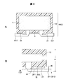
図1のAは、第1の実施の形態に係るコンデンサの一部を示している。図1のAに示す構成は一例であり、斯かる構成に本発明が限定されるものではない。
コンデンサ2はたとえば、固体電解コンデンサであり、本発明のコンデンサの一例である。
このコンデンサ2にはたとえば、円筒形に巻回されたコンデンサ素子4が用いられる。このコンデンサ素子4では一例として、陽極側の電極箔、第1のセパレータ、陰極側の電極箔および第2のセパレータを積層し、これらを円筒状に巻回した後、電解質を含浸させている。このコンデンサ素子4の陽極側の電極箔には陽極側のリード端子、陰極側の電極箔には陰極側のリード端子が接続されている。これらリード端子はコンデンサ素子4の素子端面6から引き出されている。図示しているリード端子8は陽極側または陰極側のリード端子のいずれでもよい。
コンデンサ素子4は、絶縁性樹脂による樹脂モールドが施され、樹脂層10で被覆されている。コンデンサ素子4から引き出されたリード端子8は、樹脂層10を貫通して引き出されている。
リード端子8には、金型による成形加工により、伸び部12、ノッチ14および平坦部16が形成されている。伸び部12は成形加工によりリード端子8に生じた伸延箇所であり、樹脂層10との境界部に生成されている。伸び部12は樹脂層10とノッチ14との間の間隔部の一例であり、棒状の同径部分である。ノッチ部14は薄肉部の一例である。
ノッチ14はリード端子8に形成された薄肉部の一例である。このノッチ14は、伸び部12との間に第1の段差部18-1、平坦部16との間に第2の段差部18-2を備えている。各段差部18-1、18-2は、たとえばリード端子8の中心軸Oと直交方向ないし交差方向に形成された立壁面を含んでいる。
段差部18-1の高さをa、ノッチ14の幅をbとすれば、幅bは高さaに対し、a<bの関係に設定する。つまり、幅bは高さaよりも大きく設定されている。
このようなノッチ14が形成されたリード端子8をノッチ14の段差部18-1側でノッチ方向に折り曲げる。図1のBは、段差部18-1とノッチ14との角部で折り曲げられたリード端子8を示している。
斯かる位置でリード端子8を折り曲げれば、図1のCに示すように、屈曲部20が形成されることにより、段差部18-1にノッチ14が重ねられ、リード端子8を樹脂層10のリード端子引出し面22に平行に配置することができる。この屈曲部20は、たとえばノッチ14の一部またはノッチ14と段差部18-1との境界部分に設定され、ノッチ14と段差部18-1とを両辺とした「V」字形状に形成される。この場合、段差部18-1の高さaよりノッチ14の幅bが大きいので、ノッチ14の段差部18-2がリード端子8の壁面を越えて配置され、ノッチ14の段差部18-2は伸び部12側に移動している。つまり、伸び部12の一部がノッチ14の内部に入り込むことで、ノッチ14が伸び部12を囲い込むように配置され、この実施の形態では、伸び部12の側面が段差部18-2と平行状態となる。
<第1の実施の形態の効果>
(1) リード端子8の折曲げ位置を段差部18-1とノッチ14が交差するV字状の屈曲部20に特定させることで、リード端子8の折曲げ精度を高めることができる。
(2) リード端子8はスプリングバックを生じることなく、樹脂層10のリード端子引出し面22に平行位置まで折り曲げることができる。このようなリード端子8を備えたコンデンサ2によれば、実装基板に対する配置精度の安定化を図ることができる。
(3) コンデンサ2の高さを一定にすることができ、低背化に寄与する。
〔第2の実施の形態〕
図2のAは、第2の実施の形態に係るコンデンサ2を示している。図2のAにおいて、図1のAと同一部分には同一符号を付してある。
第1の実施の形態では、伸び部12が同径の棒状であるのに対し、第2の実施の形態では、半球形状の湾曲部を備えている。このため、段差部18-1は湾曲面部で形成されている。
斯かる構成とすれば、リード端子8には、段差部18-1に角部がなく、湾曲面部であることから、図2のBに示すように、段差部18-1とノッチ14との境界部分である角部を折曲げ起点としてリード端子8を折り曲げて屈曲部20が形成される。この折り曲げの際に、段差部18-1が屈曲部20の形成に伴って変形することで段差部18-2から逃げ、両者の干渉を避けることができる。
斯かる構成では、段差部18-1の高さa、ノッチ14の幅bとを、a≧bの関係に設定することができ、ノッチ14の幅bを小さくすることができる。
斯かる構成とすれば、ノッチ14の幅bを小さくしても、ノッチ14と段差部18-1との成す角部でリード端子8を折り曲げることができ、リード端子8のスプリングバックを回避することができる。
その他の構成は第1の実施の形態と同様であるので、同一符号を付してその説明を割愛する。
<第2の実施の形態の効果>
(1)幅の狭い薄肉部であるノッチ14と湾曲面部からなる段差部18-1の成す角部を折曲げ起点にしてリード端子8を折り曲げることができ、リード端子8のスプリングバックを回避しつつリード端子8を樹脂層10のリード端子引出し面22に平行に折り曲げることができる。これにより第1の実施の形態と同様に、リード端子8の折曲げ精度を高めることができる。
(2) 第1の実施の形態と同様に、コンデンサ2の高さが均一化するので、実装基板の実装面に対するコンデンサ2の固定位置の精度を向上させることができる。
〔第3の実施の形態〕
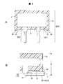
図3のAは、固体電解コンデンサの断面を示している。図3のAに示す構成は一例であり、斯かる構成に本発明が限定されるものではない。
従来、リード端子は、平坦化処理時に生じた伸び部の長さが一様にならないため樹脂層の外面に沿って折り曲げても、伸び部の長さによって樹脂層の外面と平行にならず、コンデンサの高さにばらつきが生じる可能性があった。
また、基板配置の安定性を持たせるためにリード端子に平坦化処理を施した場合、所望の箇所に平坦化を行える一方で、リード端子には平坦面と樹脂面からの導出部の間に伸び部が生じる。この伸び部と平坦面の境が折り曲げ位置となる。伸び部の長さは一様にならないので、折り曲げ位置にもばらつきが生じる。伸び部が長く、樹脂面から離れた位置が折り曲げ位置となる場合には、リード端子の折り曲げ角度はより鋭角になりやすく、リード端子の基板配置の安定性が損なわれる可能性があった。
そこで、この実施の形態のコンデンサは、リード端子の折り曲げにより生じた伸び部の長さに関係なく、リード端子の折り曲げ角度を制限する手段を備える。図3のAに示す固体電解コンデンサ30(以下単に「コンデンサ30」と称する)は、本発明のコンデンサの一例である。このコンデンサ30には、円筒形に巻回されたコンデンサ素子4が用いられる。このコンデンサ素子4の陽極側の電極箔には陽極側のリード端子32-1、陰極側の電極箔には陰極側のリード端子32-2が接続されている。これらリード端子32-1、32-2はコンデンサ素子4の素子端面6から引き出されている。
コンデンサ素子4には、絶縁性樹脂からなる外装樹脂として樹脂層10により樹脂モールドが施されている。つまり、コンデンサ素子4の外面は、樹脂層10により被覆され、樹脂層10の層内に密封されている。したがって、コンデンサ素子4の素子端面6の各リード端子32-1、32-2は、樹脂層10を貫通させて引き出されている。樹脂層10は各リード端子32-1、32-2の壁面に密着している。図3のAに示す状態は、各リード端子32-1、32-2が折曲げ加工前の状態であり、樹脂層10のリード端子引出し面22に対して垂直状態となっている。
図3のBは、図3のAのIIIB部を拡大して示している。リード端子32-1はたとえば、円柱状のワイヤで形成されている。このリード端子32-1には、リード端子本体34、伸び部36、ノッチ部38および突起部40が形成されている。リード端子32-1には、リード端子本体34が樹脂層10の層内に貫通し、樹脂層10から露出する根元側と先端部との間に伸び部36、ノッチ部38および突起部40が備えられている。ノッチ部38および突起部40はリード端子32-1、32-2の平坦面部42に形成されている。この平坦面部42はたとえば平坦部の一例であって、丸棒状のリード端子材を加圧して平坦面化した部分である。
リード端子本体34は、樹脂層10で保持されている。伸び部36は、本発明の間隔部の一例であり、リード端子32-1の根元側から先端部に向かって放物線状に偏平化して延伸している。この伸び部36は、たとえばリード端子32-1に加圧成形によりノッチ部38を形成した際に形成される。
ノッチ部38は、リード端子32-1に対する加圧成形により形成された偏平部分であり、本発明の薄肉部の一例である。この実施の形態では、ノッチ部38には第1のノッチ部38-1および第2のノッチ部38-2が形成されている。ノッチ部38-1およびノッチ部38-2は、段差を設けて厚みが異なり、先端部側のノッチ部38-2がノッチ部38-1より厚く形成されている。つまり、ノッチ部38-2および突起部40は複数の突起部の一例である。したがって、リード端子32-1の終端部にある突起部40は他の突起部であるノッチ部38-2に対して高さの異なる突起部であり、また他の突起部より高い突起部を構成している。
突起部40は、ノッチ部38-2の終端側に形成され、リード端子32-1の終端部を形成している。この突起部40は、ノッチ部38-2より厚く形成されている。
ここで、伸び部36の幅(伸び部幅)をW、ノッチ部38-1の長さ(ノッチ部長)をL1、ノッチ部38-2の長さ(ノッチ部長)をL2、ノッチ部38-1の深さ(ノッチ部深さ)をT1、ノッチ部38-2の深さ(ノッチ部深さ)をT2、陽極側リード端子32-1のリード端子の側面とノッチ部38-1の深さの差をT3とする。これらの大小関係は、たとえば次の通りである。
W<L1
W≦T1+T2
T1=T2またはT1≠T2
T3≦L1
W≦T1+T2
T1=T2またはT1≠T2
T3≦L1
この場合、ノッチ部38-2を基準とした突起部40の高さはT2であり、ノッチ部38-1を基準とした突起部40の高さはT1+T2である。つまり、伸び部36が薄肉部であるノッチ部38-1に収納された状態となる。
リード端子32-1について述べたが、リード端子32-2もリード端子32-1と同様であるので、その説明を割愛する。この折り曲げによりリード端子32-1、32-2は、突起部40がリード端子引出し面22の近傍に配置される。
図4のAは、折曲げ加工したリード端子32-1、32-2を含むコンデンサ30を示している。各リード端子32-1、32-2は反対方向に折り曲げられ、コンデンサ30の樹脂層10のリード端子引出し面22の近傍に配設されている。
図4のBは、図4のAに示すリード端子32-1側を拡大して示している。リード端子線32-1は、リード端子32-2と反対方向に折り曲げられている。この折曲げ加工はノッチ部38-1の内側で行われている。このため、ノッチ部38-1側には伸び部36が変形して入り込み、ノッチ部38-1とリード端子引出し面22との間、ノッチ部38-2とリード端子引出し面22との間には、空間44が形成されている。この場合、突起部40はリード端子引出し面22に密着し、リード端子32-1の長手方向の中心線Yは、リード端子引出し面22と平行に維持されている。これにより、コンデンサ30の高さHは一様になっている。
<第3の実施の形態の効果>
(1) リード端子32-1、32-2の先端側に突起部40を設けて、樹脂層10のリード端子引出し面22に配置したことで伸び部36の幅Wの長短に関係なく、リード端子32-1、32-2の折曲げによる跳ね上がりが防止できる。そしてリード端子32-1、32-2は、折り曲げ角度を一定に保つことができ、コンデンサ30の高さのばらつきが軽減できる。つまり、幅Wが大きい場合には、たとえば突起部40が樹脂層10のリード端子引出し面22側に当たることで、折り曲げられる角度は制限される。そのため、伸び部36の幅Wが大きくなり、折り曲げの起点がリード端子引出し面22から離れてもリード端子32-1、32-2の折り曲げ角度が大きくなることを防ぎ、回路基板に対する配置精度が安定する。
(2) コンデンサ30の高さが一定になるのでコンデンサ2を固定する回路基板に対する配置精度が向上する。
(3) 伸び部36からリード端子32-1、32-2の終端側に向かって高さが異なるノッチ部38または突起部40が備えられ、ノッチ部38と突起部40でたとえば、2段階の段差を形成すれば、樹脂層10のリード端子引出し面22に対しノッチ部38側でリード端子32-1、32-2が接触するのを防止できる。この結果、折り曲げられたリード端子32-1、32-2の折曲げ角度を一様にでき、コンデンサ30の高さのばらつきを低減できる。さらに、2段階の段差の場合、伸び部36と突起部40との間のノッチ部38の厚さが厚い部分を設けることで、リード端子の強度を保つことができる。つまり、高さが異なる段差を設ける構造は、リード端子を折り曲げ加工する際に、リード端子32-1、32-2がノッチ部38側でリード端子引出し面22に接触することを防ぐ構造であるとともに、リード端子32-1、32-2の強度を保つために必要な厚さを確保できる構造である。
(4) ノッチ部38-1、38-2が段階的に深く形成されることで、リード端子32-1、32-2の加工時の加工ストレスが低減される。つまり、薄肉部とするノッチ部38-1を深く形成して、複数段とすることで、潰し歪みの発生を防ぎ、リード端子32-1、32-2の強度を維持できる。
(5) さらに、ノッチ部38-1として形成した薄肉部は、リード端子32-1、32-2の厚さが最も薄い部分となるので、折り曲げ加工の際に起点となる。これにより折り曲げ位置を薄肉部とすることができる。このようにすることで、コンデンサ30の高さのばらつきをより軽減できる。
(6) この実施の形態の伸び部36の幅Wは、たとえばリード端子32-1、32-2の強度や加工数を考慮し、W=0.02ないし0.1〔mm〕とすることが好ましい。
〔第4の実施の形態〕
図5のAは、第4の実施の形態に係る固体電解コンデンサを示している。図5のAにおいて、図4と同一部分には同一符号を付してある。
この実施の形態のコンデンサ30は、たとえば樹脂層10のリード端子引出し面22の縁部側に突起部46が形成されている。この突起部46の高さは薄肉部の一例である既述のノッチ部38-2の深さ、つまり、ノッチ部38-2の底面からの突起部40の高さT2と同等に設定すればよい。
斯かる構成とすれば、図5のBに示すように、リード端子32-1、32-2を互いに反対方向にノッチ部38で屈曲させ、折曲げ加工を施せば、リード端子32-1、32-2の側壁がリード端子引出し面22に形成される突起部46の近傍に配置される。この場合、リード端子32-1、32-2は、一部が突起部46に当たり、リード端子32-1、32-2の折り曲げ角度を制限できるので、リード端子32-1、32-2が水平に維持される。つまり、リード端子32-1、32-2の跳ね上がりが防止され、リード端子32-1、32-2は、たとえば長手方向の中心を示す中心線Yが平坦側のリード端子引出し面22と平行に維持される。これにより、コンデンサ30の高さHを一様に維持することができる。
<第4の実施の形態の効果>
(1) このコンデンサ30は、リード端子32-1、32-2の導出面にあるリード端子引出し面22側に設けた突起部46に対してリード端子32-1、32-2を配置している。リード端子32-1、32-2は、たとえば突起部46に対して平坦部が接触することで、折り曲げられる角度が制限される。これによりリード端子32-1、32-2は、伸び部36の幅Wの長短に関係なく、リード端子32-1、32-2の折曲げ位置を一定に保つことができ、曲げ高さのばらつきを軽減できる。
(2) リード端子32-1、32-2の曲げ状態を安定させることで、コンデンサ30の高さが均一化するので、基板に実装されるコンデンサ30の固定位置精度が向上する。
〔他の実施の形態〕
(1) 上記実施の形態では、一例として、固体電解コンデンサを例示したが、本発明のコンデンサは電解コンデンサなどの他のコンデンサであってもよい。
(2) 以上説明したように、本発明の最も好ましい実施の形態等について説明した。本発明は、上記記載に限定されるものではない。特許請求の範囲に記載され、または発明を実施するための形態に開示された発明の要旨に基づき、当業者において様々な変形や変更が可能である。斯かる変形や変更が、本発明の範囲に含まれることは言うまでもない。
本発明は、樹脂モールドにより樹脂層で被覆された固体電解コンデンサなどのコンデンサであって、リード端子の成形精度を高めることができ、実装基板に対する位置精度の向上やコンデンサの高さの安定化が図れる。
2、30 コンデンサ
4 コンデンサ素子
6 素子端面
8 リード端子
10 樹脂層
12、36 伸び部
14 ノッチ
16 平坦部
18-1 第1の段差部
18-2 第2の段差部
20 屈曲部
22 リード端子引出し面
32-1 陽極側のリード端子
32-2 陰極側のリード端子
34 リード端子本体
38 ノッチ部
40、46 突起部
42 平坦面部
44 空間
4 コンデンサ素子
6 素子端面
8 リード端子
10 樹脂層
12、36 伸び部
14 ノッチ
16 平坦部
18-1 第1の段差部
18-2 第2の段差部
20 屈曲部
22 リード端子引出し面
32-1 陽極側のリード端子
32-2 陰極側のリード端子
34 リード端子本体
38 ノッチ部
40、46 突起部
42 平坦面部
44 空間
Claims (9)
- リード端子を接続したコンデンサ素子を樹脂で被覆したコンデンサであって、
前記コンデンサ素子を覆う樹脂層から導出された前記リード端子に、
前記樹脂層の外面から露出する間隔部と、
薄肉部と、
前記間隔部と前記薄肉部との境界部である段差部とを備え、
前記薄肉部を前記段差部に向かって折り曲げて前記樹脂層側に配置された前記リード端子は、前記段差部と前記薄肉部が重ねられ、かつ、前記薄肉部が前記間隔部を囲むように配置されていることを特徴とするコンデンサ。 - 前記段差部の高さが前記薄肉部の幅より小さく設定されていることを特徴とする請求項1に記載のコンデンサ。
- さらに、前記リード端子の側面部分、または前記リード端子が導出された前記樹脂層の外面側に突起部が形成され、
前記リード端子の折曲げにより、前記樹脂層の外面部の近傍に前記リード端子の前記突起部が配置されまたは前記リード端子と対向する前記樹脂層に形成された前記突起部の近傍に前記リード端子が配置されることを特徴とする請求項1または請求項2に記載のコンデンサ。 - 前記リード端子の前記突起部が前記リード端子の折り曲げにより前記樹脂層の外面側の樹脂面に当たり、または前記リード端子が前記樹脂層の前記突起部に当たり、前記リード端子の折り曲げ角度が前記リード端子の前記突起部または前記樹脂層の前記突起部により制限されることを特徴とする請求項3に記載のコンデンサ。
- 前記リード端子の終端部と、前記薄肉部との間に高さの異なる複数の突起部を備え、これら突起部のうち、終端側の突起部の高さを他の突起部より高く設定したことを特徴とする請求項1ないし請求項4のいずれか1項に記載のコンデンサ。
- リード端子を接続したコンデンサ素子を樹脂で被覆したコンデンサの製造方法であって、
前記コンデンサ素子を覆う樹脂層から導出された前記リード端子に、前記樹脂層の外面から露出する間隔部を設定し、
前記間隔部との間に段差部を設けるとともに前記リード端子に薄肉部を形成し、
前記薄肉部で前記段差部に向かって前記リード端子を折り曲げ、前記段差部と前記薄肉部が重なり、かつ、前記薄肉部が前記間隔部を囲むように配置する 処理を含むことを特徴とするコンデンサの製造方法。 - 前記段差部の高さを前記薄肉部の幅より小さく形成する処理を含むことを特徴とする請求項6に記載のコンデンサの製造方法。
- さらに、前記リード端子の側面部分、または前記リード端子が導出された前記樹脂層の外面側に突起部を形成し、
前記リード端子の折曲げにより、前記樹脂層の外面部の近傍に前記リード端子の前記突起部を配置し、または前記リード端子と対向する前記樹脂層に形成された前記突起部の近傍に前記リード端子を配置させる処理を含むことを特徴とする請求項6または請求項7に記載のコンデンサの製造方法。 - 前記リード端子の前記突起部が前記リード端子の折り曲げにより前記樹脂層の外面側の樹脂面に当たり、または前記リード端子が前記樹脂層の前記突起部に当たり、前記リード端子の折り曲げ角度を前記リード端子の前記突起部または前記樹脂層の前記突起部により制限させる処理を含むことを特徴とする請求項8に記載のコンデンサの製造方法。
Priority Applications (2)
| Application Number | Priority Date | Filing Date | Title |
|---|---|---|---|
| CN201480004927.0A CN104919553A (zh) | 2013-01-18 | 2014-01-17 | 电容器及其制造方法 |
| US14/799,923 US20150318117A1 (en) | 2013-01-18 | 2015-07-15 | Capacitor and manufacturing method therefor |
Applications Claiming Priority (4)
| Application Number | Priority Date | Filing Date | Title |
|---|---|---|---|
| JP2013-007093 | 2013-01-18 | ||
| JP2013007093A JP6179102B2 (ja) | 2013-01-18 | 2013-01-18 | コンデンサおよびその製造方法 |
| JP2013-075751 | 2013-04-01 | ||
| JP2013075751A JP2014203834A (ja) | 2013-04-01 | 2013-04-01 | コンデンサおよびその製造方法 |
Related Child Applications (1)
| Application Number | Title | Priority Date | Filing Date |
|---|---|---|---|
| US14/799,923 Continuation US20150318117A1 (en) | 2013-01-18 | 2015-07-15 | Capacitor and manufacturing method therefor |
Publications (1)
| Publication Number | Publication Date |
|---|---|
| WO2014112385A1 true WO2014112385A1 (ja) | 2014-07-24 |
Family
ID=51209479
Family Applications (1)
| Application Number | Title | Priority Date | Filing Date |
|---|---|---|---|
| PCT/JP2014/000214 Ceased WO2014112385A1 (ja) | 2013-01-18 | 2014-01-17 | コンデンサおよびその製造方法 |
Country Status (4)
| Country | Link |
|---|---|
| US (1) | US20150318117A1 (ja) |
| CN (1) | CN104919553A (ja) |
| TW (1) | TWI611444B (ja) |
| WO (1) | WO2014112385A1 (ja) |
Families Citing this family (2)
| Publication number | Priority date | Publication date | Assignee | Title |
|---|---|---|---|---|
| CN107240500A (zh) * | 2017-04-21 | 2017-10-10 | 南通星晨电子有限公司 | 一种贴片电容的制造方法 |
| JP2019134044A (ja) * | 2018-01-30 | 2019-08-08 | トヨタ自動車株式会社 | コンデンサモジュール |
Citations (4)
| Publication number | Priority date | Publication date | Assignee | Title |
|---|---|---|---|---|
| JPS62162323A (ja) * | 1986-01-13 | 1987-07-18 | 松下電器産業株式会社 | 電子部品 |
| JPH03225913A (ja) * | 1990-01-31 | 1991-10-04 | Elna Co Ltd | アルミニウム電解コンデンサ |
| JPH0499807U (ja) * | 1991-02-06 | 1992-08-28 | ||
| JPH05335171A (ja) * | 1992-05-29 | 1993-12-17 | Nippon Chemicon Corp | 電子部品 |
Family Cites Families (2)
| Publication number | Priority date | Publication date | Assignee | Title |
|---|---|---|---|---|
| JP2585132B2 (ja) * | 1990-08-15 | 1997-02-26 | 松下電工株式会社 | 粉末焼結品の製造方法 |
| JP4958694B2 (ja) * | 2007-09-04 | 2012-06-20 | 三洋電機株式会社 | 固体電解コンデンサ |
-
2014
- 2014-01-17 WO PCT/JP2014/000214 patent/WO2014112385A1/ja not_active Ceased
- 2014-01-17 TW TW103101786A patent/TWI611444B/zh active
- 2014-01-17 CN CN201480004927.0A patent/CN104919553A/zh active Pending
-
2015
- 2015-07-15 US US14/799,923 patent/US20150318117A1/en not_active Abandoned
Patent Citations (4)
| Publication number | Priority date | Publication date | Assignee | Title |
|---|---|---|---|---|
| JPS62162323A (ja) * | 1986-01-13 | 1987-07-18 | 松下電器産業株式会社 | 電子部品 |
| JPH03225913A (ja) * | 1990-01-31 | 1991-10-04 | Elna Co Ltd | アルミニウム電解コンデンサ |
| JPH0499807U (ja) * | 1991-02-06 | 1992-08-28 | ||
| JPH05335171A (ja) * | 1992-05-29 | 1993-12-17 | Nippon Chemicon Corp | 電子部品 |
Also Published As
| Publication number | Publication date |
|---|---|
| TW201440101A (zh) | 2014-10-16 |
| CN104919553A (zh) | 2015-09-16 |
| TWI611444B (zh) | 2018-01-11 |
| US20150318117A1 (en) | 2015-11-05 |
Similar Documents
| Publication | Publication Date | Title |
|---|---|---|
| US10468204B2 (en) | Capacitor and manufacturing method therefor | |
| CN105469995B (zh) | 固体电解电容器 | |
| JP5971943B2 (ja) | コンデンサ | |
| WO2018020993A1 (ja) | 電解コンデンサ | |
| KR20090100247A (ko) | 칩형 콘덴서 | |
| WO2014112385A1 (ja) | コンデンサおよびその製造方法 | |
| JP5853750B2 (ja) | コンデンサおよびその製造方法 | |
| JP2011049225A (ja) | 固体電解コンデンサ | |
| JP6531134B2 (ja) | 電解コンデンサ用リード線端子、電解コンデンサ用リード線端子の製造方法、及び電解コンデンサ | |
| CN102222570B (zh) | 电解电容器及其制造方法 | |
| JP6179102B2 (ja) | コンデンサおよびその製造方法 | |
| JP5915588B2 (ja) | コイル及びコイルの製造方法 | |
| JP2017220485A (ja) | ケースレスフィルムコンデンサ | |
| JP2004247410A (ja) | チップ型固体電解コンデンサ及びその製造方法 | |
| JP2014203834A (ja) | コンデンサおよびその製造方法 | |
| JP2016046388A (ja) | コンデンサおよびその製造方法 | |
| US6826034B2 (en) | Vibration-resistant electrochemical cell, and method for the production thereof | |
| JP2013026293A (ja) | コンデンサおよびその製造方法 | |
| JP2013201259A (ja) | 端子成形方法、端子およびコンデンサの製造方法 | |
| JP5261538B2 (ja) | 固体電解コンデンサ | |
| JP6083159B2 (ja) | コンデンサおよびその製造方法 | |
| JP2012069631A (ja) | 電解コンデンサ | |
| JP5898927B2 (ja) | チップ型固体電解コンデンサ | |
| CN107644737B (zh) | 电解电容器用引线端子及其制造方法、以及电解电容器 | |
| JP2024104255A (ja) | コンデンサ |
Legal Events
| Date | Code | Title | Description |
|---|---|---|---|
| 121 | Ep: the epo has been informed by wipo that ep was designated in this application |
Ref document number: 14740334 Country of ref document: EP Kind code of ref document: A1 |
|
| NENP | Non-entry into the national phase |
Ref country code: DE |
|
| 122 | Ep: pct application non-entry in european phase |
Ref document number: 14740334 Country of ref document: EP Kind code of ref document: A1 |