WO2014104367A1 - バスバー及びバスバーモジュール、並びにバスバーの製造方法 - Google Patents
バスバー及びバスバーモジュール、並びにバスバーの製造方法 Download PDFInfo
- Publication number
- WO2014104367A1 WO2014104367A1 PCT/JP2013/085268 JP2013085268W WO2014104367A1 WO 2014104367 A1 WO2014104367 A1 WO 2014104367A1 JP 2013085268 W JP2013085268 W JP 2013085268W WO 2014104367 A1 WO2014104367 A1 WO 2014104367A1
- Authority
- WO
- WIPO (PCT)
- Prior art keywords
- bus bar
- conductor wire
- conductor
- strip
- laminated
- Prior art date
- Legal status (The legal status is an assumption and is not a legal conclusion. Google has not performed a legal analysis and makes no representation as to the accuracy of the status listed.)
- Ceased
Links
Images








Classifications
-
- H—ELECTRICITY
- H01—ELECTRIC ELEMENTS
- H01B—CABLES; CONDUCTORS; INSULATORS; SELECTION OF MATERIALS FOR THEIR CONDUCTIVE, INSULATING OR DIELECTRIC PROPERTIES
- H01B7/00—Insulated conductors or cables characterised by their form
- H01B7/30—Insulated conductors or cables characterised by their form with arrangements for reducing conductor losses when carrying alternating current, e.g. due to skin effect
-
- H—ELECTRICITY
- H01—ELECTRIC ELEMENTS
- H01B—CABLES; CONDUCTORS; INSULATORS; SELECTION OF MATERIALS FOR THEIR CONDUCTIVE, INSULATING OR DIELECTRIC PROPERTIES
- H01B13/00—Apparatus or processes specially adapted for manufacturing conductors or cables
- H01B13/06—Insulating conductors or cables
- H01B13/08—Insulating conductors or cables by winding
- H01B13/0891—After-treatment
-
- H—ELECTRICITY
- H01—ELECTRIC ELEMENTS
- H01B—CABLES; CONDUCTORS; INSULATORS; SELECTION OF MATERIALS FOR THEIR CONDUCTIVE, INSULATING OR DIELECTRIC PROPERTIES
- H01B7/00—Insulated conductors or cables characterised by their form
- H01B7/02—Disposition of insulation
- H01B7/0241—Disposition of insulation comprising one or more helical wrapped layers of insulation
-
- H—ELECTRICITY
- H01—ELECTRIC ELEMENTS
- H01B—CABLES; CONDUCTORS; INSULATORS; SELECTION OF MATERIALS FOR THEIR CONDUCTIVE, INSULATING OR DIELECTRIC PROPERTIES
- H01B7/00—Insulated conductors or cables characterised by their form
- H01B7/30—Insulated conductors or cables characterised by their form with arrangements for reducing conductor losses when carrying alternating current, e.g. due to skin effect
- H01B7/306—Transposed conductors
-
- H—ELECTRICITY
- H01—ELECTRIC ELEMENTS
- H01B—CABLES; CONDUCTORS; INSULATORS; SELECTION OF MATERIALS FOR THEIR CONDUCTIVE, INSULATING OR DIELECTRIC PROPERTIES
- H01B13/00—Apparatus or processes specially adapted for manufacturing conductors or cables
- H01B13/0006—Apparatus or processes specially adapted for manufacturing conductors or cables for reducing the size of conductors or cables
-
- H—ELECTRICITY
- H01—ELECTRIC ELEMENTS
- H01B—CABLES; CONDUCTORS; INSULATORS; SELECTION OF MATERIALS FOR THEIR CONDUCTIVE, INSULATING OR DIELECTRIC PROPERTIES
- H01B5/00—Non-insulated conductors or conductive bodies characterised by their form
- H01B5/02—Single bars, rods, wires, or strips
- H01B5/04—Single bars, rods, wires, or strips wound or coiled
-
- Y—GENERAL TAGGING OF NEW TECHNOLOGICAL DEVELOPMENTS; GENERAL TAGGING OF CROSS-SECTIONAL TECHNOLOGIES SPANNING OVER SEVERAL SECTIONS OF THE IPC; TECHNICAL SUBJECTS COVERED BY FORMER USPC CROSS-REFERENCE ART COLLECTIONS [XRACs] AND DIGESTS
- Y10—TECHNICAL SUBJECTS COVERED BY FORMER USPC
- Y10T—TECHNICAL SUBJECTS COVERED BY FORMER US CLASSIFICATION
- Y10T29/00—Metal working
- Y10T29/49—Method of mechanical manufacture
- Y10T29/49002—Electrical device making
- Y10T29/49117—Conductor or circuit manufacturing
- Y10T29/49174—Assembling terminal to elongated conductor
Definitions
- the present invention relates to a bus bar and a bus bar module used for electrical connection, and a method for manufacturing the bus bar.
- bus bars and bus bar modules are used for electrical connection.
- a bus bar and a bus bar module are used for electrical connection in which a pulse width modulation (PWM) drive control with a high frequency current is performed in a hybrid vehicle or an electric vehicle.
- PWM pulse width modulation
- a bus bar used in a hybrid vehicle system will be described based on Patent Documents 1 and 2.
- a bus bar is used between the motor and the motor inverter, between the generator and the generator inverter, and for electrical connection of the power line in the inverter unit.
- a high-frequency current flowing between a motor or a generator and an inverter includes a high-frequency component of several kHz associated with switching in addition to a basic sine wave and a direct current component.
- a high frequency component induces an eddy current inside the conductor of the bus bar.
- the skin depth ⁇ ( ⁇ / ⁇ f ⁇ ) obtained from the conductor material of the bus bar 101 composed of the current frequency f and the rectangular wire due to the skin effect.
- a current concentrates and flows under the surface of the surface having a depth of 1/2 . As a result, the current density flowing inside the conductor is reduced, and the effective resistance of the conductor is increased, resulting in an eddy current loss.
- FIG. 10 shows a graph showing the relationship between the frequency of the drive current and the skin depth for various conductor materials.
- a bus bar used in a motor or the like that uses a high voltage and large current as shown in Patent Document 1 is a copper flat bus bar having a large surface area. It is used. However, a basic sine wave and a direct current component having a relatively low frequency, which are main electric power, also flow through the bus bar. Therefore, if the cross-sectional area is reduced to a flat plate shape in order to suppress high-frequency components, the effective resistance to the current carrying the main power increases, and so-called copper loss (iron loss when the material is iron) increases. It will be.
- a flat plate-like metal plate such as copper having a certain thickness has not a little rigidity, and its forming process and mounting wiring are not easy. Therefore, how to reduce transmission loss comprehensively in a bus bar that transmits a current in which high frequency is mixed from low frequency is a problem.
- the high-frequency component associated with PWM induces a reactive voltage (V ⁇ f ⁇ L) proportional to the product of inductance and frequency on the bus bar. Therefore, when switching is fast, the surge causes a large withstand voltage to the output stage element of the inverter. You will be forced to request. Therefore, it is desirable that the stray inductance of the bus bar or bus bar module is as small as possible.
- Patent Document 2 a set rectangular wire obtained by collecting a plurality of relatively thin rectangular wires in parallel constitutes a bus bar.
- Patent Document 2 claims that this reduces manufacturing costs, facilitates the formation of complex shapes, and can also suppress eddy current loss by diverting to each rectangular wire.
- the wire diameter is reduced to (1 / the number of coil wires) as compared with the case where the bus bar is configured by a flat plate.
- eddy current loss which is said to be proportional to the square of the line width, is suppressed, and as a result, eddy current loss is reduced in the entire bus bar.
- each wire diameter is reduced by increasing the number of wires, the loop of the eddy current flowing through the cross section can be reduced and the eddy current loss can be further reduced.
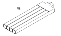
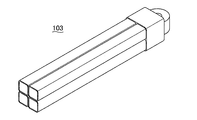
- the bus bar 102 is constituted by a plurality of square lines arranged in parallel as shown in FIG. 12A, the skin effect remains. That is, as shown in FIG. 12B, assuming that the high-frequency current supplied from the outside is equally distributed to each square line constituting the bus bar 102, and considering the high-frequency magnetic flux line excited thereby, the inner square line The presence of magnetic flux lines surrounding Since the square lines on both sides of the magnetic flux line are connected by the terminals at both ends of the bus bar 102, a large closed loop is formed, and the alternating magnetic flux line penetrates the loop. Due to the electromagnetic induction action in this situation, an induced electromotive force is generated in the closed loop, and an eddy current flows.
- Patent Document 2 improves shape workability and mounting wiring property, but does not exhibit any effect in suppressing eddy current loss.
- Patent Document 2 describes that it is possible to further reduce the overcurrent loss by twisting the entire assembly of a plurality of rectangular wires.
- this configuration does not affect the shape and distribution of the flux lines in the cross-sectional views shown in FIGS. 12B and 13B.
- the effect of reducing the eddy current induced by the AC flux lines and the accompanying power loss is not. It turns out that there is nothing.
- twisting the entire assembly of a plurality of rectangular wires is equivalent to having an internal inductance like a solenoid coil, and therefore increases the inductance more than necessary.
- an object of the present invention is to provide a bus bar and a bus bar module that can reduce eddy current loss due to a high-frequency current, and a method for manufacturing the bus bar.
- a bus bar according to the present invention is a bus bar used for electrical connection, in which one or more strip conductors covered with an insulating film are arranged adjacent to each other in the width direction of the strip conductor.
- two conductor wires configured in a flat plate shape are arranged side by side in close proximity or in close contact with each other in the spiral while winding in the longitudinal direction, and the outer surfaces in the width direction are arranged in parallel.
- each of the strip-like conductors of the two conductor wires is the outer surface of the laminated conductor wire and the laminated conductor wire is inside the laminated conductor wire.
- the belt-like conductor on the surface of the laminated conductor wire enters inside at the next pitch due to the spirally wound structure. For this reason, current flows through each strip conductor without distinction between the outside and inside of the laminated conductor wire, ensuring an effective cross-sectional area, minimizing eddy current loss, and effectively suppressing the skin effect of high-frequency current it can.
- the two conductor wires are spirally wound so that one or more strip conductors covered with an insulating film are arranged adjacent to each other in the width direction of the strip conductor.
- the first conductor wire configured in a flat plate shape by adjoining or closely contacting the wound internal surfaces and one or more strip conductors coated with an insulating film are adjacent in the width direction of the strip conductor.
- a second conductor wire configured in a flat plate shape while being wound in a spiral shape in the opposite direction to the first conductor wire so as to be close to or in close contact with the opposite surfaces of the wound inside. Good.
- the strip conductors of the first conductor wire and the second conductor wire constituting the bus bar are wound in spirals in opposite directions with respect to each other, and the internal inductance increases due to the coil-like spiral current flowing.
- the first conductor wire in which the belt-like conductor is wound in a spiral shape and the second conductor wire in which the belt-like conductor is wound in a spiral shape in the opposite direction are laminated side by side in the longitudinal direction.
- the resulting magnetic flux lines spreading around each are globally offset. Therefore, an increase in internal inductance of the entire bus bar can be minimized.
- the number of the strip conductors constituting each of the two conductor wires may be equal, and the strip conductors constituting each of the two conductor wires may have the same width. . Furthermore, the number of the strip-shaped conductors constituting each of the two conductor lines may be two.
- the first conductor wire and the second conductor wire can be regarded as two solenoid coils having the same number of turns through which turning currents in opposite directions flow. And these two solenoid coils are arrange
- the simple structure has an effect that molding and mounting wiring are easy. Furthermore, when the number of the strip-shaped conductors constituting each of the two conductor lines is two and the strip-shaped conductors have the same width, the bus bar width and the spiral pitch can be combined appropriately. And since the number of parts is the smallest, it is most preferable in the molding process and the mounting wiring.
- the aspect ratio of the thickness to the width of the laminated conductor wire may be 1 or less.
- the cross-sectional shape in the width direction of the laminated conductor wire is changed from a square to a rectangle.
- the bus bar having the conventional rectangular wire structure has the smallest surface area of the bus bar, and eddy current loss is reduced.
- the strip conductors of the first conductor wire and the second conductor wire are interchanged between the outside of the bus bar and the inside of the bus bar along the longitudinal direction of the bus bar. Since the current flows without distinction inside, the effective area can be secured, the eddy current loss can be suppressed small, and the skin effect of the high frequency current can be effectively suppressed.
- the bus bar according to the present invention is such that the width of the laminated conductor wire is W, the thickness of the laminated conductor wire is T, the width of the strip conductor is ⁇ , and half the spiral pitch of the strip conductor is ⁇ .
- the skin depth ⁇ ( ⁇ / ⁇ f ⁇ ) 1/2 obtained from the frequency f of the current to be passed through, the resistivity ⁇ and the magnetic permeability ⁇ of the strip conductor, and the dimensional ratio of T / W and ⁇ / W
- the combination may satisfy the following formula (1).
- the cross-sectional shape in the width direction with respect to the AC resistance of the bus bar according to the present invention has substantially the same dimension.
- the ratio value of the AC resistance of the bus bar having the conventional rectangular wire structure is 1 or less. Thereby, AC resistance can be reduced (improved).
- the bus bar according to the present invention is such that the ratio ⁇ t / Tt of Tt to Tt is 1 or less, where ⁇ t is the gap between the first conductor wire and the second conductor wire and Tt is the thickness of the strip conductor. May have a ratio.
- the gap between the first conductor wire in which the strip conductors constituting the spiral of the bus bar are spirally wound and the second conductor wire in which the strip conductors are spirally wound in the opposite direction is narrowed.
- the bus bar according to the present invention may be used for an electrical connection for passing a pulse-width modulated current.
- a current having a remarkably large high-frequency component flows to the bus bar, and the eddy current loss becomes significant in the bus bar having a conventional rectangular wire structure.
- eddy current loss can be reduced by using the bus bar according to the present invention.
- bus bar according to the present invention may be used for electrical connection between the electric motor and the inverter.
- the drive current supplied from the inverter to the electric motor contains not a few switching noises accompanying the pulse width modulation, that is, harmonic components.
- eddy current loss can be reduced.
- bus bar module according to the present invention is characterized in that a plurality of bus bars according to the present invention formed in a predetermined shape are closely assembled so that the surfaces in the width direction face each other and are integrally assembled and assembled. To do.
- the bus bar can be used for driving a three-phase motor or the like by integrating, for example, three bus bars into a bus bar module.
- the bus bar manufacturing method is a bus bar manufacturing method for manufacturing a bus bar used for electrical connection, wherein one or a plurality of strip conductors covered with an insulating film are arranged in the width direction of the strip conductor.
- a conductor wire rolling process that constitutes a conductor wire and the two conductor wires are arranged in parallel in the longitudinal direction, and are laminated so that the surfaces in the width direction face each other to form a laminated conductor wire
- a terminal portion joining step of arranging terminal portions for electrical connection on both ends of the laminated conductor wire and joining the two conductor wires.
- each of the strip-like conductors of the two conductor wires is the outer surface of the laminated conductor wire and the laminated conductor wire is inside the laminated conductor wire.
- the belt-like conductor on the surface of the laminated conductor wire enters the inside at the next pitch due to the spirally wound structure. Therefore, current flows through each strip conductor without distinction between the outside and inside of the laminated conductor wire, the effective area can be secured, eddy current loss can be kept small, and the skin effect of high-frequency current can be effectively suppressed. .
- the conductor wire winding step is spirally arranged so that one or more strip conductors covered with an insulating film are arranged adjacent to each other in the width direction of the strip conductor.
- a first conductor wire winding step of forming a first conductor wire winding body by winding in the shape of a wire, and one or more strip conductors covered with an insulating film arranged adjacent to each other in the width direction of the strip conductor A second conductor wire winding step of forming a second conductor wire winding body by winding in a spiral shape in the opposite direction to the first conductor wire, and the conductor wire rolling step includes rolling
- the first conductor wire winding body is formed into a flat plate shape by processing to form a first conductor wire
- the second conductor wire winding body is formed into a flat plate shape by rolling to form a second conductor wire
- the first conductor wire and the second conductor wire are respectively connected in the longitudinal direction.
- the terminal portion joining step includes connecting the terminal portion for electrical connection to the laminated conductor wire. You may arrange
- each strip conductor is wound spirally in the opposite direction with respect to each other, and the internal inductance increases due to the flow of a coil-like spiral current, but the strip conductor is wound spirally.
- One conductor wire and a second conductor wire in which a strip-like conductor is wound in a spiral shape in the opposite direction are laminated side by side in the longitudinal direction. For this reason, the magnetic flux lines that spread around each of them are globally offset, so that an increase in internal inductance of the entire bus bar can be minimized.
- the bus bar module According to the bus bar, the bus bar module, and the bus bar manufacturing method of the present invention, it is possible to reduce eddy current loss accompanying high-frequency current.
- bus bar and the bus bar module and the method for manufacturing the bus bar according to the present invention are not limited to the following embodiments, and various modifications are possible as long as they are described in the claims.
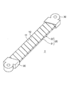
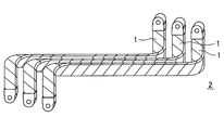
- the bus bar 1 shown in FIG. 1 and the bus bar module 2 shown in FIG. 8 are used for electrical connection, and in particular, used for electrical connection for energizing a pulse-width modulated (PWM) current.
- PWM pulse-width modulated
- a bus bar and a bus bar module are used for connection between various electrical devices such as electrical connection with a power source and electrical connection between various control devices.
- a bus bar and a bus bar module according to the present embodiment, and a method for manufacturing the bus bar will be described.
- FIG. 1 is a perspective view showing a bus bar according to the present embodiment.
- FIG. 2 is a perspective sectional view showing a part of the laminated conductor wire constituting the bus bar according to the present embodiment.
- FIG. 3 is a longitudinal sectional view of the laminated conductor wire constituting the bus bar according to the present embodiment.
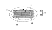
- FIG. 4A is a cross-sectional view in the width direction of the laminated conductor wire constituting the bus bar according to the present embodiment.
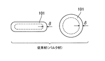
- FIG. 4B is a cross-sectional view in the width direction of the bus bar according to the related art.
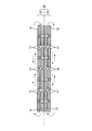
- FIG. 5 is a top view showing the dimensions of the laminated conductor wire constituting the bus bar according to the present embodiment.
- FIG. 6 is a graph showing combinations of geometric parameters T / W and ⁇ / W applied in the bus bar according to the present embodiment.
- FIG. 7 is a top view showing the dimensions of the laminated conductor wire constituting the bus bar according to the present embodiment.
- the bus bar 1 includes a laminated conductor wire 20 composed of two conductor wires, a first conductor wire 21 and a second conductor wire 22, and terminal portions arranged on both ends of the laminated conductor wire 20. 30.
- the terminal portion 30 is joined to the first conductor wire 21 and the second conductor wire 22 and arranged on both ends of the laminated conductor wire 20. And the terminal part 30 is connected to each corresponding terminal part, such as an electrically connected inverter and a power supply.
- the first conductor wire 21 is formed by adjoining two strip conductors 11 and 12 having the same width ⁇ and thickness covered with an insulating film in the width direction of the strip conductors 11 and 12. As arranged, it is formed by being spirally wound at a helical pitch of 2 ⁇ .
- the spiral pitch means the length of the spiral axis per one rotation of the spiral.
- the first conductor wire 21 is formed in a flat plate shape having a width W and a thickness T / 2 by bringing the opposed surfaces of the wound inside close to or in close contact with each other.
- the second conductor wire 22 includes two strip conductors 11 and 12 having the same width ⁇ and thickness covered with an insulating film and adjacent to each other in the width direction of the strip conductors 11 and 12.
- the first conductor wire 21 is wound in a spiral shape with a spiral pitch of 2 ⁇ so as to be arranged.
- the second conductor wire 22 is formed in a flat plate shape having a width W and a thickness T / 2 by bringing the opposite surfaces of the wound inside close to or in close contact with each other.
- the strip-shaped conductors 11 and 12 are made of any one of aluminum, copper, an aluminum alloy, and a copper alloy, or these are the main materials.
- aluminum for example, 1060 (pure aluminum) can be applied. If 1060 (pure aluminum) is used for the strip conductors 11 and 12, the conductivity is further improved.
- the aluminum alloy for example, 6061 (aluminum added with a small amount of manganese and silicon) can be used. If an aluminum alloy is used for the conductor, the strength is further improved.
- copper include oxygen-free copper (OFC) and tough pitch copper.
- the copper alloy examples include a precipitation-type copper alloy obtained by adding a small amount of iron and phosphorus to copper, specifically, for example, “KFC” (registered trademark). If this "KFC” (registered trademark) is used for the strip conductors 11 and 12, the adhesiveness between the strip conductors 11 and 12 and the insulating film (not shown) can be increased, and the insulating film can be made difficult to peel off. Yes (interfacial peel strength can be increased).
- the insulating film is made of a mixture of an organic material and an inorganic material or an organic material. This organic material is composed of one or more selected from, for example, a thermoplastic resin, a thermosetting resin, and rubber.
- the inorganic material include crystalline silica powder, fused silica powder, glass fiber, talc powder, mica powder, aluminum oxide powder, magnesium oxide powder, aluminum nitride powder, boron nitride powder, silicon nitride powder, and silicon carbide. It consists of 1 type or multiple types chosen from powder.
- the insulating film is not necessarily limited to a film material that is stuck or sandwiched, and may be an enamel or formal coating film formed by a polymerization process such as application and subsequent heating. Further, if the conductor is aluminum, it may be an oxide film formed on the surface by oxalic acid treatment or anodizing treatment. Then, an arbitrary material is selected according to the bus bar 1.
- the laminated conductor wire 20 has a first conductor wire 21 and a second conductor wire 22 juxtaposed in the longitudinal direction, and the outer surfaces of the first conductor wire 21 and the second conductor wire 22 in the width W direction are mutually connected. It is formed by stacking so as to face each other.
- the laminated conductor wire 20 is configured in a flat plate shape having a width W and a thickness T.
- the laminated conductor wire 20 is configured so that the aspect ratio of the thickness T to the width W of the laminated conductor wire 20 is 1 or less (T ⁇ W). That is, the laminated conductor wire 20 may be configured such that the aspect ratio of the thickness T to the width W of the laminated conductor wire 20 is 1, and the cross section in the width direction is substantially square. Alternatively, the laminated conductor wire 20 may be configured such that the aspect ratio of the thickness T to the width W of the laminated conductor wire 20 is less than 1, and the cross section in the width direction is a substantially flat rectangular shape.
- the width of the laminated conductor wire 20 is W
- the thickness of the laminated conductor wire 20 is T
- the width of the strip conductors 11 and 12 is ⁇
- Formula (1) shows the geometrical conditions for the bus bar 1 according to the present embodiment to reduce the AC resistance and suppress the eddy current loss as compared with the bus bar in the prior art.
- the ratio formula (1) is the AC resistance R AC busbar according to the present embodiment shown in FIG. 7, for the AC resistance R AC bulk of the bus bar of the conventional rectangular wire structure width direction of the cross-sectional shape which is substantially the same size It is developed and arranged so that ⁇ (f) is 1 or less.
- the calculation process is represented by the following formula (2).
- the AC resistance R AC of the bus bar 1 according to the present embodiment has the AC resistance R of a bus bar having a conventional rectangular wire structure in which the cross-sectional shape in the width direction is substantially the same. Less than AC bulk . That is, a ratio ⁇ (f) smaller than 1 means that eddy current loss is reduced.
- the bus bar 1 according to the present embodiment has a combination of T / W and ⁇ / W dimensional ratios that satisfy Equation (1), so that the bus bar 1 according to the present embodiment is compared with the bus bar in the prior art, The AC resistance is reduced, the notation effect is suppressed, and eddy current loss is suppressed.
- Equation (3) the bus bar AC resistance R AC of having dimensions of laminated conductor lines shown in FIG. 5, the AC resistance R AC bulk of the bus bar of the conventional rectangular wire structure width direction of the cross-sectional shape which is substantially the same size
- the ratio ⁇ (f) with respect to is expanded and arranged so as to be 1 or less.
- the calculation process is represented by the following formula (4).
- the equation (2) derived from the equation (4) is a dimensionless geometric parameter g (T / W, ⁇ / W) that defines the structure of the bus bar 1 according to the present embodiment, and (the thickness of the bus bar 1). Expressed as a product of twice the skin depth (2 ⁇ / T) made dimensionless (divided by T).
- values where the geometric parameter g (T / W, ⁇ / W) is 1.2 to 2.0 are defined as contour lines on a two-dimensional plane of (T / W) ⁇ ( ⁇ / W). Indicates what is expressed.
- the side where the value obtained by multiplying the value of the contour line by the value of 2 ⁇ / T is 1 or less defines the geometrical shape that can obtain the effect of reducing and improving the eddy current loss for the bus bar 1 according to this embodiment. Yes.
- the right side of FIG. 6 shows an example of the shape according to the aspect ratio. When the aspect ratio T / W is 0.1, the shape is flat, and when the aspect ratio T / W is 1, the shape is flat. Or cylindrical.
- the ratio of ⁇ t to Tt ⁇ t / Tt is 1 or less, where ⁇ t is the gap between the first conductor wire 21 and the second conductor wire 22 and Tt is the thickness of the strip conductors 11 and 12. .
- the current flowing in each of the strip conductors 11 and 12 wound in a spiral shape in the opposite direction with respect to each other has an angle with respect to the longitudinal direction of the laminated conductor wire 20. It can be divided into components perpendicular to it. As shown in FIG.
- the two strip-like conductors 11, 11 of the first conductor wire 21 and the second conductor wire 22 arranged above and below in the thickness direction and 12 and 12 are the outside of the laminated conductor wire 20 (the surface of the laminated conductor wire 20) and the inside (the inside of the laminated conductor wire 20, that is, the laminated surface on which the first conductor wire 21 and the second conductor wire 22 are laminated). It flows in the longitudinal direction while changing. That is, the strip-like conductors 11 and 12 on the surface of the laminated conductor wire 20 enter the inside at the next pitch by the structure wound in a spiral shape in the opposite direction with respect to each other.
- FIG. 4B shows the current distribution in the case of conventional bulk material bus bars (rectangular and circular). As shown in FIG. 4B, in the conventional bulk material bus bar, the high-frequency current is concentrated in the thin layer of the surface subcutaneous ⁇ due to the skin effect in both the rectangular shape and the circular shape.
- FIG. 3 when viewed in a longitudinal section of the laminated conductor wire 20 (that is, the bus bar 1), two of the first conductor wire 21 and the second conductor wire 22 arranged above and below in the thickness direction.
- the pair can be regarded as two solenoid coils having swirl currents in opposite directions. If these two solenoid coils are arranged sufficiently close to each other, the magnetic flux lines formed outside thereof are opposite to each other, and the first conductor wire 21 and the second conductor wire 22 are the two conductor wires 20. If you superimpose the two, they will cancel out.
- the internal inductance generated with the structure of the bus bar 1 according to the present embodiment is proportional to the spread of magnetic flux lines generated by the high-frequency current, that is, the volume integral of the magnetic flux density. Therefore, the bus bar 1 according to the present embodiment has an effect that the magnetic flux lines do not spread outside the bus bar 1 and the internal inductance is suppressed to the minimum.
- the strip conductors 11 and 12 of the first conductor wire 21 and the second conductor wire 22 are arranged along the longitudinal direction of the laminated conductor wire 20 constituting the bus bar 1.
- the surface of the laminated conductor wire 20 that is the outer side and the inside of the laminated conductor wire 20 that is the inner side are interchanged. Therefore, since current flows through each of the strip conductors 11 and 12 without distinction between the outside and inside of the laminated conductor wire 20, an effective cross-sectional area can be secured, eddy current loss can be suppressed, and the skin effect of high-frequency current can be reduced. Can be effectively suppressed.
- belt-shaped conductor 11 and 12 is wound by the spiral shape of the opposite direction with respect to each other, and an internal inductance increases when a coil-like spiral current flows.
- the first conductor wire 21 in which the strip conductors 11 and 12 are spirally wound and the second conductor wire 22 in which the strip conductors 11 and 12 are spirally wound in the direction opposite to the first conductor wire 21. Are laminated side by side in the longitudinal direction, and the generated magnetic flux lines spreading around each of them are globally offset. Therefore, an increase in internal inductance of the bus bar 1 as a whole can be minimized.
- the eddy current loss is suppressed to avoid the skin effect, and not only the low-frequency current but also the high-frequency current is allowed to flow inside the bus bar 1 so that the current can flow through the entire cross-sectional area in a wide frequency region.
- transmission loss can be effectively suppressed from a low-frequency fundamental wave to a high frequency accompanying modulation.
- the internal inductance generated with the structure of the laminated conductor wire 20 constituting the bus bar 1 is proportional to the spread of the magnetic flux line caused by the high frequency current, that is, the volume integral of the magnetic flux density. Therefore, magnetic flux lines are present on the bus bar of the laminated conductor wire 20 formed by laminating two pairs of flat conductor wires of the first conductor wire 21 and the second conductor wire 22 that are reversely wound with respect to each other and have the same number of turns. There is an effect that the internal inductance is suppressed to the minimum without spreading outside the bus bar 1.
- the number of the strip conductors 11 and 12 constituting each of the first conductor line 21 and the second conductor line is two and the width is the same, a simple structure capable of appropriately combining the bus bar width and the spiral pitch. It is. And since the number of parts is the smallest, it is most preferable in the molding process and the mounting wiring.
- bus bar module The bus bar module according to the present embodiment will be described with reference to FIGS. 8A and 8B.
- 8A and 8B are perspective views showing the bus bar module according to the present embodiment.
- FIGS. 8A and 8B show a bus bar module 2 in which three bus bars 1 according to the present embodiment are integrated as a set.
- FIG. 8A shows a straight type
- FIG. 8B shows a crank type.
- the bus bar module 2 can be mounted and wired arbitrarily by combining a straight type and a crank type. Moreover, by adding a twist deformation to the straight portion of the bus bar module 2, flexibility and flexibility in the angle of the connection direction can be ensured.
- the bus bar module 2 integrates three bus bars 1 as a set, the bus bar module 2 is not limited to this, and a plurality of bus bars 1 may be integrated as a set.
- the effective inductance of the bus bar module 2 is the sum of the internal inductance of each bus bar 1 and the external inductance derived from the spatial circuit formed by the arrangement of the three bus bars 1.
- the former internal inductance is minimized by the structure of the bus bar 1 according to this embodiment described above.
- the external inductance of the latter is proportional to the interval between the three bus bars 1, but the minimum is achieved by making the cross section of the bus bar 1 flat and flat, and overlapping the surfaces in the width direction without any gaps. It can be suppressed to the limit.
- FIGS. 8A and 8B by adding torsional deformation to the straight portion of the bus bar module 2, the flexibility and the degree of freedom of the connection angle can be ensured while the external inductance is secured. Can be minimized.
- the three bus bars 1 can be integrated and assembled into the bus bar module 2 to be used for driving a three-phase motor or the like.
- FIGS. 9A to 9D are perspective views showing the procedure of the steps of the bus bar manufacturing method according to the present embodiment.
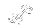
- the first conductor wire winding step (conductor wire winding step) two strip conductors 11 and 12 covered with an insulating film are adjacent to each other in the width direction of the strip conductors 11 and 12.
- the 1st conductor wire winding body 21a which is one of the two conductor wire winding bodies is formed.
- the first conductor wire 21 is configured by forming the first conductor wire winding body 21a into a flat plate shape by rolling. By this rolling process, the opposed surfaces inside the wound first conductor wire winding body 21a are brought close to or in close contact with each other, and the flat first conductor wire 21 is formed.
- the two strip conductors 11 and 12 covered with the insulating film are arranged in the width direction of the strip conductors 11 and 12.
- the coil is wound in a spiral shape opposite to the first conductor wire 21.
- the 2nd conductor wire winding body 22a which is one of two conductor wire winding bodies is formed.
- the second conductor wire 22 is formed by forming the second conductor wire winding body 22a into a flat plate shape by rolling. By this rolling process, the opposed surfaces inside the wound second conductor wire winding body 22a are brought close to or in close contact with each other, so that the flat second conductor wire 22 is formed.
- the first conductor wire 21 and the second conductor wire 22 are juxtaposed in the longitudinal direction, and are superposed such that the surfaces in the width direction face each other.
- the laminated conductor wire 20 is formed by laminating.
- the terminal portions 30 for electrical connection are arranged on both ends of the laminated conductor wire 20 and joined to the first conductor wire 21 and the second conductor wire 22. To do.
- the strip conductors 11 of the first conductor wire 21 and the second conductor wire 22 along the longitudinal direction of the laminated conductor wire 20 constituting the bus bar 1, 12 is switched between the surface of the laminated conductor wire 20 that is the outside of the laminated conductor wire 20 and the inside of the laminated conductor wire 20 that is inside the laminated conductor wire 20. That is, the strip conductors 11 and 12 on the surface of the laminated conductor wire 20 enter the inside at the next pitch due to the structure in which the conductors are wound spirally or spirally in the opposite direction.
- each of the strip conductors 11 and 12 is wound in a spiral shape or a spiral shape in the opposite direction, and the internal inductance increases when a coil-like spiral current flows.
- the bus bar 1 As described above, the eddy current loss is suppressed to avoid the skin effect, and not only the low frequency current but also the high frequency current can flow inside the bus bar, and the current can flow through the entire cross-sectional area in a wide frequency region. Thereby, transmission loss can be effectively suppressed from a low-frequency fundamental wave to a high frequency accompanying modulation.
- the first conductor wire 21 and the second conductor wire 22 are wound in a spiral shape in opposite directions with respect to each other, but are not limited thereto. That is, in order to suppress the eddy current and minimize the inductance, the bus bar 1 is composed of the first conductor wire 21 and the second conductor wire 22 wound in a spiral shape in opposite directions with respect to each other. It is necessary. However, if the inductance may be somewhat large, either of the same two conductor wires in which the bus bar 1 is spirally wound in the same direction (that is, either the first conductor wire 21 or the second conductor wire 22). It may be constituted by.
- the first conductor wire winding body 21a in which the strip conductors 11 and 12 are spirally wound in the first conductor wire winding step is manufactured, and the second conductor wire winding is performed.
- belt-shaped conductors 11 and 12 in the spiral shape of the reverse direction to the 1st conductor wire winding body is manufactured at the rotation process, it is not restricted to it. That is, in order to suppress the eddy current and minimize the inductance, the bus bar 1 is composed of the first conductor wire 21 and the second conductor wire 22 wound in a spiral shape in the opposite direction to each other. is required.
- the bus bar 1 is configured by either one of the same two conductor wires wound in a spiral shape in the same direction (either the first conductor wire 21 or the second conductor wire 22). May be. Further, as the conductor wire winding step, either the first conductor wire winding step or the second conductor wire winding step was performed twice, and the strip conductors 11 and 12 were wound in a spiral shape in the same direction. Two conductor wire winding bodies (first conductor wire winding body 21a or second conductor wire winding body 22a) may be manufactured.
- the conductor wire rolling process step is performed on the first conductor wire winding body 21a while performing the first conductor wire winding step, and the second conductor wire winding is performed. While conducting the process, the conductor wire rolling process is performed on the second conductor wire wound body 22a, but is not limited thereto. That is, after performing the first conductor wire winding step and the second conductor wire winding step, the conductor wire rolling step is performed on each of the first conductor wire winding body 21a and the second conductor wire winding body 22a. You can go.
- the number of the strip conductors constituting each of the first conductor wire 21 and the second conductor wire 22 is the same, and the strip conductors constituting each have the same width. 11 and 12, but is not limited thereto. That is, the first conductor line 21 and the second conductor line 22 may be configured by one band-shaped conductor having the same width, as long as the band-shaped conductors are arranged adjacent to each other in the width direction. You may be comprised with the above strip
- belt-shaped conductors which comprise the 1st conductor wire 21, and the number of the 2nd conductor wires 22 may differ, and the width
- the number of the strip conductors constituting each of the first conductor wire 21 and the second conductor wire 22 is the same, and the strip conductors constituting each have the same width, a simple structure can be formed or mounted. There is an effect that wiring is easy.
- the width of the bus bar 1 becomes narrower than the width of the strip conductor, or the length in the longitudinal direction of the bus bar 1 becomes longer than necessary, and the AC resistance is smaller than that of the conventional bus bar (for example, a bulk material bus bar).
- the shape is very limited. That is, in the bus bar 1 according to the present embodiment, it is preferable that the first conductor wire 21 and the second conductor wire 2 are composed of two or more strip conductors from the viewpoint of molding and mounting wiring.
- the structure is simple because the width of the bus bar and the helical pitch can be combined as appropriate, and the number of parts is minimized. Most preferable in processing and mounting wiring.
- bus bar module 2 described above describes a straight type and a crank type, it is not limited thereto. You may form in arbitrary shapes according to the place which installs a bus-bar module.
- terminal portion 30 of the bus bar 1 is not limited to the shape shown in FIG. 1, and various shapes of terminal portions 30 can be used.
- the frequency dependence of the AC resistance was measured using a copper plate having a total thickness of 0.6 mm, which is thinner than 1 mm to several mm, which is the thickness of a practical product actually used as the bus bar 1.
- the first conductor line 21 and the second conductor line 22 are formed by the two strip-shaped conductors 11 and 12 having a thickness of 0.15 mmt and a width of 19 mmW.
- the 1st conductor wire 21 and the 2nd conductor wire 22 were stuck, the laminated conductor wire 20 of thickness 0.6mmtx width 19mmW was manufactured, and the bus bar 1 manufactured by joining the terminal part 30 was used.
- the bus bar 1 according to the first example was manufactured so that the total length was 6 mL.
- FIG. 14 shows the measurement results for the first example and three samples in bulk and four layers.
- the measurement result of the bus bar 1 according to the first embodiment is “this example”
- the measurement result of the bulk material bus bar is “bulk”
- the measurement result of the four-layer bus bar is “four sheets”. It is described.
- the Ls and Rs values of the three samples at the low frequency are approximately the same value.
- a scale indicating the ratio between the skin depth ⁇ and the total thickness t of the bus bar is clearly shown.
- the normalized inductance ⁇ L> shows a constant value regardless of the frequency with good accuracy.
- the bus bar 1 according to the first embodiment has a much smaller value in the region where the skin depth ⁇ is 1/2 to 1/10 of the bus bar total thickness t compared to the bulk bus bar and the four-layer bus bar. It turns out that it becomes remarkable (it exhibits low resistance).
- skin depth ⁇ is the thickness of strip conductors 11 and 12 constituting bus bar 1 according to the present embodiment (here Is 0.15 mmt) or less. At this time, a higher-order skin effect occurs in the constituent conductor, and it is expected that the effect of reducing the eddy current loss due to the high-frequency current is somewhat reduced.
- the bus bar 1 according to the second example was manufactured by the following procedure. First, the strip conductors 11 and 12 having a thickness of 0.3 mm were spirally wound with a space of 0.4 mm provided therebetween. Thus, the first conductor wire 21 and the second conductor wire 22 having a thickness of 1.0 mmt ⁇ a width of 19 mmW were formed.
- the space between the strip conductors 11 and 12 is the gap between the opposing surfaces of the wound strip conductors 11 and 12, that is, the space inside the first conductor wire 21 and the second conductor wire 22. Means that.
- the second conductor wire 22 was wound in a spiral shape in the opposite direction with respect to the first conductor wire 21.
- the first conductor wire 21 and the second conductor wire 22 were brought into close contact with each other with a space of 0.3 mm therebetween to produce a laminated conductor wire 20 having a thickness of 2.3 mmt ⁇ width of 19 mmW.
- the bus bar 1 which concerns on the 2nd Example was manufactured by pinching the laminated conductor wire 20 15 mm with the copper terminal part 30 of thickness 6mmtx width 19mmWx length 30mmL.
- the bus bar 1 according to the second example was manufactured so that the total length was 334 mm.
- the frequency dependency of the AC resistance was also analyzed for the bulk material bus bar as with the bus bar 1 according to the second example.
- the bulk material bus bar was manufactured by the following procedure. First, a conductor wire having a thickness of 1.2 mmt ⁇ width of 19 mmW ⁇ total length of 304 mmL was manufactured so as to have the same cross-sectional area as the bus bar 1 according to the second example. Next, 15 mm of the conductor wire was sandwiched between the copper terminal portion 30 having a thickness of 6 mm, a width of 19 mm, and a length of 30 mm to manufacture a bulk material bus bar. And like the bus bar 1 which concerns on a 2nd Example, the bulk material bus bar was manufactured so that full length might be 334 mm.
- the frequency dependence of the AC resistance was also analyzed for the four-layer bus bar in the same manner as the bus bar 1 according to the second example.
- the four-layer bus bar was manufactured by the following procedure. First, a set of four rectangular wires having a thickness of 0.3 mmt ⁇ width 19 mmW (the same width as the bus bar 1 according to the second embodiment) ⁇ the total length 304 mmL (the same length as the bus bar 1 according to the second embodiment) in parallel I let you. Next, as with the bus bar 1, the thickness between the outermost rectangular wire and the adjacent one of the adjacent rectangular wires is set to 0.4 mmt, and the gap between the inner rectangular wires is set to 0.3 mmt.
- a four-layer bus bar was manufactured using a set of rectangular wires sandwiching 15 mm of the four rectangular wires with a copper terminal portion 30 of thickness 6 mm ⁇ width 19 mm ⁇ length 30 mm. Similar to the bus bar 1 according to the second embodiment, the four-layer bus bar was manufactured to have a total length of 334 mm.
- the frequency dependence of the AC resistance was also analyzed for the four-layer thin bus bar in the same manner as the bus bar 1 according to the second embodiment.
- the four-ply thin bus bar was manufactured by attaching the terminal part 30 to the above-described four-ply bus bar with all the gaps of the rectangular wires being 0.1 mmt.
- FIG. 15 shows the result of analyzing the frequency dependence of the AC resistance Rs by the quasi-electrostatic magnetic field analysis by the three-dimensional boundary element method, and the frequency dependence of the AC resistance Rs is measured as a resistance value.
- FIG. 16 is a graph obtained by enlarging the frequency characteristic of the AC resistance ACR near the skin depth of the graph shown in FIG.
- the measurement result of the bus bar 1 according to the second embodiment is “this example”
- the measurement result of the bulk material bus bar is “bulk”
- the measurement result of the four-layer bus bar is “4 sheets”.
- the measurement result of the “overlap”, four-layer thin bus bar is described as “four-layer thin”.
- the AC resistance Rs is smaller than that of the bulk bus bar.
- the AC resistance Rs of the four-ply thin bus bar in which the gap between the flat wires is smaller than the thickness of the flat wire is smaller than the four-ply bus bar in which the gap between the flat wires is equal to or greater than the thickness of the flat wire. It is the same level. Based on the above analysis results, the effect of suppressing the increase in internal inductance was confirmed by reducing the gap between the flat wires, that is, by making the gap between the flat wires smaller than the thickness of the flat wire.
- the gap between the strip conductors 11 and 12 is reduced, that is, the gap between the first conductor wire 21 and the second conductor wire 22 is ⁇ t, and the thickness of the strip conductors 11 and 12 is increased.
- Tt it can be predicted that an effect of suppressing an increase in internal inductance can be obtained by setting the ratio ⁇ t / Tt of ⁇ t to Tt to 1 or less.
- the bus bar 1 according to the second embodiment is compared with the bulk material bus bar, the 4-layer bus bar, and the 4-layer thin bus bar in the region where the skin depth ⁇ is 1/2 to 1/10.
- the AC resistance ACR is a small value. From this analysis result, it was confirmed that the bus bar 1 according to the second example was able to reduce the eddy current loss accompanying the high frequency current.
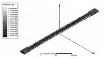
- FIGS. 17 shows a current density distribution of the bus bar 1 according to the second embodiment.
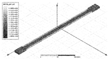
- FIG. 18 shows the current density distribution of the bulk bus bar.
- the current density on the conductor surface is broadly and averagely distributed as compared with the bulk bus bar. This shows that, in the bus bar 1 according to the second embodiment, the high-frequency current of 30 MHz flows to the inside of the laminated conductor wire 20, so that the effective cross-sectional area is widened and the surface layer current density is reduced. ing.
Landscapes
- Engineering & Computer Science (AREA)
- Manufacturing & Machinery (AREA)
- Inverter Devices (AREA)
- Non-Insulated Conductors (AREA)
- Installation Of Bus-Bars (AREA)
- Windings For Motors And Generators (AREA)
Abstract
Description

本実施形態に係るバスバーについて、図1~図7に基づいて説明する。図1は、本実施形態に係るバスバーを示す斜視図である。図2は、本実施形態に係るバスバーを構成する積層導体線の一部を示す斜視断面図である。図3は、本実施形態に係るバスバーを構成する積層導体線の長手方向の断面図である。図4Aは、本実施形態に係るバスバーを構成する積層導体線の幅方向の断面図である。図4Bは、従来技術に係るバスバーの幅方向の断面図である。図5は、本実施形態に係るバスバーを構成する積層導体線の寸法を示す上面図である。図6は、本実施形態に係るバスバーで適用する幾何パラメータT/W、λ/Wの組み合わせを示すグラフである。図7は、本実施形態に係るバスバーを構成する積層導体線の寸法を示す上面図である。


本実施形態に係るバスバーモジュールについて、図8A及び図8Bに基づいて説明する。図8A及び図8Bは、本実施形態に係るバスバーモジュールを示す斜視図である。
本実施形態に係るバスバーの製造方法について、図9A~図9Dに基づいて説明する。図9A~図9Dは、本実施形態に係るバスバーの製造方法の工程の手順を示す斜視図である。
本実施形態に係るバスバー1の第一の実施例について、交流抵抗解析を行った。その結果について、以下、図14に基づいて具体的に説明する。
次に、本実施形態に係るバスバー1の第二の実施例について、交流抵抗解析と電流密度分布解析を行った。その結果について、以下、図15~図18に基づいて具体的に説明する。
第二の実施例に係るバスバー1、バルク材バスバー、4枚重ねバスバー、4枚重ね薄バスバーについて、交流抵抗の周波数依存性の解析を行った。図15及び図16は、その結果を示す。図15は、3次元境界要素法による準静電磁界解析による交流抵抗Rsの周波数依存性について解析した結果であり、交流抵抗Rsの周波数依存性が抵抗値として計測されている。図16は、図15に示すグラフのスキンデプス付近の交流抵抗ACRの周波数特性を拡大したグラフである。尚、図15及び図16では、第二の実施例に係るバスバー1の計測結果を「本実施例」、バルク材バスバーの計測結果を「バルク」、4枚重ねバスバーの計測結果を「4枚重ね」、4枚重ね薄バスバーの計測結果を「4枚重ね薄」として記載している。
また、上記の第二の実施例に係るバスバー1及びバルクバスバーについて、30MHzの高周波電流を流した際の電流密度分布の解析を行った。その結果を、図17及び図18に示す。図17は、第二の実施例に係るバスバー1の電流密度分布を示す。また、図18は、バルクバスバーの電流密度分布を示す。
2 バスバーモジュール
11 帯状導体
12 帯状導体
20 積層導体線
21 第1導体線(2つの導体線)
21a 第1導体線巻回体(2つの導体線巻回体)
22 第2導体線(2つの導体線)
22a 第2導体線巻回体(2つの導体線巻回体)
30 端子部
Claims (12)
- 電気接続に用いられるバスバーであって、
絶縁膜で被覆された1つまたは複数の帯状導体を当該帯状導体の幅方向において隣接して配列するように螺旋状に巻回しつつ、巻回した内部の対向する表面を近接または密着させて平板状に構成した2つの導体線を、それぞれの長手方向に並設し、それぞれの幅方向の外部の表面が互いに対向するように重ね合わせて積層させた積層導体線と、
前記積層導体線の両端側に配置し、前記2つの導体線に接合させた、電気接続するための端子部と、
を備えることを特徴とするバスバー。 - 前記2つの導体線は、
絶縁膜で被覆された1つまたは複数の帯状導体を当該帯状導体の幅方向において隣接して配列するように螺旋状に巻回しつつ、巻回した内部の対向する表面を近接または密着させて平板状に構成した第1導体線と、
絶縁膜で被覆された1つまたは複数本の帯状導体を当該帯状導体の幅方向において隣接して配列するように前記第1導体線とは反対方向の螺旋状に巻回しつつ、巻回した内部の対向する表面を近接または密着させて平板状に構成した第2導体線と、からなることを特徴とする請求項1に記載のバスバー。 - 前記2つの導体線のそれぞれを構成する前記帯状導体の数が等しく、前記2つの導体線のそれぞれを構成する前記帯状導体が等しい幅を有することを特徴とする請求項1に記載のバスバー。
- 前記2つの導体線のそれぞれを構成する前記帯状導体の数が2つであることを特徴とする請求項3に記載のバスバー。
- 前記積層導体線の幅に対する厚みのアスペクト比が1以下であることを特徴とする請求項1に記載のバスバー。
- 前記積層導体線の幅をW、前記積層導体線の厚みをT、前記帯状導体の幅をω、前記帯状導体の螺旋ピッチの半分をλとすると、前記バスバーに通電させる電流の周波数fと前記帯状導体の抵抗率ρ及び透磁率μから求まる表皮深さδ=(ρ/πfμ)1/2に対して、T/W及びλ/Wの寸法比の組み合わせが以下の式(1)を満たすことを特徴とする請求項1に記載のバスバー。

- 前記第1導体線と前記第2導体線の隙間をδt、前記帯状導体の厚みをTtとすると、Ttに対するδtの比率δt/Ttが1以下であることを特徴とするバスバー請求項2に記載のバスバー。
- パルス幅変調された電流を通電させる電気接続に用いられることを特徴とする請求項1に記載のバスバー。
- 電動機とインバータとの間の電気接続に用いられることを特徴とする請求項1に記載のバスバー。
- 所定の形状に形成した複数の請求項1~9のいずれか一項に記載のバスバーを、幅方向の表面が対向するように密接配置して一体化して組み立てて形成されることを特徴とするバスバーモジュール。
- 電気接続に用いられるバスバーを製造するバスバーの製造方法であって、
絶縁膜で被覆された1つまたは複数の帯状導体を当該帯状導体の幅方向において隣接して配列するように螺旋状に巻回して2つの導体線巻回体を構成する導体線巻回工程と、
圧延加工により前記2つの導体線巻回体を平板状に形成して2つの導体線を構成する導体線圧延加工工程と、
前記2つの導体線をそれぞれの長手方向に並設し、それぞれの幅方向の表面が互いに対向するように重ね合わせて積層して積層導体線を構成する積層工程と、
電気接続するための端子部を前記積層導体線の両端側に配置し、前記2つの導体線に接合する端子部接合工程と、
を備えることを特徴とするバスバーの製造方法。 - 前記導体線巻回工程は、
絶縁膜で被覆された1つまたは複数の帯状導体を当該帯状導体の幅方向において隣接して配列するように螺旋状に巻回して第1導体線巻回体を構成する第1導体線巻回工程と、
絶縁膜で被覆された1つまたは複数本の帯状導体を当該帯状導体の幅方向において隣接して配列するように前記第1導体線とは反対方向の螺旋状に巻回して第2導体線巻回体を構成する第2導体線巻回工程と、からなり、
前記導体線圧延加工工程は、
圧延加工により前記第1導体線巻回体を平板状に形成して第1導体線を構成すると共に、圧延加工により前記第2導体線巻回体を平板状に形成して第2導体線を構成し、
前記積層工程は、
前記第1導体線と前記第2導体線とをそれぞれの長手方向に並設し、それぞれの幅方向の表面が互いに対向するように重ね合わせて積層して積層導体線を構成し、
前記端子部接合工程は、
電気接続するための端子部を前記積層導体線の両端側に配置し、前記第1導体線と前記第2導体線に接合することを特徴とする請求項11に記載のバスバーの製造方法。
Priority Applications (4)
| Application Number | Priority Date | Filing Date | Title |
|---|---|---|---|
| DE112013006284.4T DE112013006284B4 (de) | 2012-12-28 | 2013-12-27 | Sammelschiene, deren Verwendung, Sammelschienenmodul und Verfahren zum Herstellen einer Sammelschiene |
| CN201380068034.8A CN104885319B (zh) | 2012-12-28 | 2013-12-27 | 母线、母线模块以及母线的制造方法 |
| US14/436,315 US9620263B2 (en) | 2012-12-28 | 2013-12-27 | Bus bar, bus bar module, and method of manufacturing bus bar |
| KR1020157016799A KR101732291B1 (ko) | 2012-12-28 | 2013-12-27 | 버스 바 및 버스 바 모듈, 및 버스 바의 제조 방법 |
Applications Claiming Priority (2)
| Application Number | Priority Date | Filing Date | Title |
|---|---|---|---|
| JP2012286995 | 2012-12-28 | ||
| JP2012-286995 | 2012-12-28 |
Publications (1)
| Publication Number | Publication Date |
|---|---|
| WO2014104367A1 true WO2014104367A1 (ja) | 2014-07-03 |
Family
ID=51021428
Family Applications (1)
| Application Number | Title | Priority Date | Filing Date |
|---|---|---|---|
| PCT/JP2013/085268 Ceased WO2014104367A1 (ja) | 2012-12-28 | 2013-12-27 | バスバー及びバスバーモジュール、並びにバスバーの製造方法 |
Country Status (6)
| Country | Link |
|---|---|
| US (1) | US9620263B2 (ja) |
| JP (1) | JP6075784B2 (ja) |
| KR (1) | KR101732291B1 (ja) |
| CN (1) | CN104885319B (ja) |
| DE (1) | DE112013006284B4 (ja) |
| WO (1) | WO2014104367A1 (ja) |
Cited By (1)
| Publication number | Priority date | Publication date | Assignee | Title |
|---|---|---|---|---|
| RU2749558C1 (ru) * | 2020-09-29 | 2021-06-15 | федеральное государственное бюджетное образовательное учреждение высшего образования «Томский государственный университет систем управления и радиоэлектроники» | Способ изготовления линии электропередачи со спиральным поперечным сечением и устройство на его основе |
Families Citing this family (18)
| Publication number | Priority date | Publication date | Assignee | Title |
|---|---|---|---|---|
| JP6075784B2 (ja) * | 2012-12-28 | 2017-02-08 | 株式会社神戸製鋼所 | バスバー及びバスバーモジュール、並びにバスバーの製造方法 |
| JP2017058275A (ja) * | 2015-09-17 | 2017-03-23 | 株式会社村田製作所 | 電流センサおよびそれを備える電力変換装置 |
| US20180097322A1 (en) * | 2016-09-30 | 2018-04-05 | Faraday&Future Inc. | Flexible bus bar |
| JP7023047B2 (ja) * | 2017-01-25 | 2022-02-21 | 日本電産コパル株式会社 | 電磁アクチュエータ |
| JP6866832B2 (ja) * | 2017-11-27 | 2021-04-28 | トヨタ自動車株式会社 | 積層平型電線の分岐構造 |
| JP6881264B2 (ja) * | 2017-12-01 | 2021-06-02 | トヨタ自動車株式会社 | 積層平型電線 |
| JP7079124B2 (ja) * | 2018-03-15 | 2022-06-01 | 古河電気工業株式会社 | 電気接続ユニット材セット |
| DE102018207587A1 (de) * | 2018-05-16 | 2019-11-21 | Robert Bosch Gmbh | Sammelschiene und elektrische Vorrichtung |
| JP7016836B2 (ja) * | 2019-06-10 | 2022-02-07 | 矢崎総業株式会社 | 導電システム |
| KR102780571B1 (ko) | 2019-08-12 | 2025-03-11 | 주식회사 엘지에너지솔루션 | 절연 및 방열 성능이 우수한 버스바 및 이를 구비한 배터리 모듈 |
| KR102244390B1 (ko) * | 2019-09-04 | 2021-04-26 | 대산전자(주) | 버스 바 |
| KR20210131156A (ko) | 2020-04-23 | 2021-11-02 | 진영글로벌 주식회사 | 열방출능력이 향상된 중공형 구조의 플렉시블 버스바, 이를 포함하는 전력공급장치 및 그 제조방법 |
| JP7123514B2 (ja) * | 2020-06-17 | 2022-08-23 | 矢崎総業株式会社 | 導電構造体 |
| US11791597B2 (en) * | 2021-02-05 | 2023-10-17 | Aptiv Technologies (2) S.À R.L. | Flexible electrical bus bar and method of manufacturing the same |
| KR102538543B1 (ko) * | 2021-04-07 | 2023-06-05 | 안희익 | 전기에너지 통전용 부스 바의 제작방법 |
| KR102818125B1 (ko) * | 2023-06-29 | 2025-06-10 | 주식회사 경신 | 방열 버스바 |
| USD1100858S1 (en) * | 2024-02-26 | 2025-11-04 | Kyungshin Corp. | Busbar for power distribution controller |
| CN118688686B (zh) * | 2024-08-22 | 2025-01-03 | 宁德时代新能源科技股份有限公司 | 连接部件的异常检测方法、装置、设备、介质和程序产品 |
Citations (6)
| Publication number | Priority date | Publication date | Assignee | Title |
|---|---|---|---|---|
| JPS50544Y1 (ja) * | 1973-03-23 | 1975-01-09 | ||
| JPS58156308U (ja) * | 1982-04-12 | 1983-10-19 | 株式会社東芝 | 閉鎖配電盤の母線連結部 |
| JPH09135565A (ja) * | 1995-09-08 | 1997-05-20 | Hitachi Ltd | 配線基板及びそれを用いてた電力変換装置 |
| JP2010246298A (ja) * | 2009-04-08 | 2010-10-28 | Sumitomo Electric Ind Ltd | バスバー,その形成方法およびバスバーモジュール |
| WO2012118047A1 (ja) * | 2011-03-02 | 2012-09-07 | 株式会社オートネットワーク技術研究所 | バスバー |
| WO2012118046A1 (ja) * | 2011-03-02 | 2012-09-07 | 株式会社オートネットワーク技術研究所 | バスバーセット及びその製造方法 |
Family Cites Families (17)
| Publication number | Priority date | Publication date | Assignee | Title |
|---|---|---|---|---|
| FR2142694B1 (ja) | 1971-06-23 | 1974-03-08 | Comp Generale Electricite | |
| US3792595A (en) * | 1972-10-26 | 1974-02-19 | Thermo King Corp | Transportable refrigeration apparatus for preserving perishables |
| US4780157A (en) | 1984-07-24 | 1988-10-25 | Phelps Dodge Industries, Inc. | Method and apparatus for manufacturing transposed ribbon cable and electromagnetic device |
| GB8505811D0 (en) * | 1985-03-06 | 1985-04-11 | Bekaert Sa Nv | Induction heating |
| JPS6216011A (ja) * | 1985-07-13 | 1987-01-24 | 富士電機株式会社 | 母線支持装置 |
| FR2719718B1 (fr) * | 1994-05-06 | 1996-06-07 | Schneider Electric Sa | Dispositif de jeu de barres, notamment pour une armoire de distribution électrique. |
| GB9715851D0 (en) * | 1997-07-29 | 1997-10-01 | Rolla Ltd | Bus bar support |
| US6005193A (en) * | 1997-08-20 | 1999-12-21 | Markel; Mark L. | Cable for transmitting electrical impulses |
| CN2300205Y (zh) * | 1997-11-12 | 1998-12-09 | 华鹏集团公司 | 母线单元连接装置 |
| US7364315B2 (en) * | 2002-06-14 | 2008-04-29 | Tseng-Lu Chien | Tubular electro-luminescent panel(s) light device |
| JP4551166B2 (ja) | 2004-09-13 | 2010-09-22 | 矢崎総業株式会社 | 機器直付けコネクタ |
| DE102004046442A1 (de) * | 2004-09-24 | 2006-04-06 | Siemens Ag | Anordnung zum Schutz von elektronischen Komponenten |
| JP4580036B1 (ja) * | 2009-06-12 | 2010-11-10 | 株式会社神戸製鋼所 | バスバーおよびコネクタ |
| PL2428967T3 (pl) * | 2010-09-08 | 2013-10-31 | Abb Schweiz Ag | Uzwojenie transformatora |
| JP5749503B2 (ja) * | 2011-01-27 | 2015-07-15 | 株式会社タムラ製作所 | コア固定具及びコイル装置 |
| DE102012217990A1 (de) * | 2012-10-02 | 2014-04-03 | Siemens Aktiengesellschaft | Supraleitende Spuleneinrichtung und Herstellungsverfahren |
| JP6075784B2 (ja) * | 2012-12-28 | 2017-02-08 | 株式会社神戸製鋼所 | バスバー及びバスバーモジュール、並びにバスバーの製造方法 |
-
2013
- 2013-12-20 JP JP2013264477A patent/JP6075784B2/ja not_active Expired - Fee Related
- 2013-12-27 WO PCT/JP2013/085268 patent/WO2014104367A1/ja not_active Ceased
- 2013-12-27 DE DE112013006284.4T patent/DE112013006284B4/de not_active Expired - Fee Related
- 2013-12-27 CN CN201380068034.8A patent/CN104885319B/zh not_active Expired - Fee Related
- 2013-12-27 US US14/436,315 patent/US9620263B2/en not_active Expired - Fee Related
- 2013-12-27 KR KR1020157016799A patent/KR101732291B1/ko not_active Expired - Fee Related
Patent Citations (6)
| Publication number | Priority date | Publication date | Assignee | Title |
|---|---|---|---|---|
| JPS50544Y1 (ja) * | 1973-03-23 | 1975-01-09 | ||
| JPS58156308U (ja) * | 1982-04-12 | 1983-10-19 | 株式会社東芝 | 閉鎖配電盤の母線連結部 |
| JPH09135565A (ja) * | 1995-09-08 | 1997-05-20 | Hitachi Ltd | 配線基板及びそれを用いてた電力変換装置 |
| JP2010246298A (ja) * | 2009-04-08 | 2010-10-28 | Sumitomo Electric Ind Ltd | バスバー,その形成方法およびバスバーモジュール |
| WO2012118047A1 (ja) * | 2011-03-02 | 2012-09-07 | 株式会社オートネットワーク技術研究所 | バスバー |
| WO2012118046A1 (ja) * | 2011-03-02 | 2012-09-07 | 株式会社オートネットワーク技術研究所 | バスバーセット及びその製造方法 |
Cited By (1)
| Publication number | Priority date | Publication date | Assignee | Title |
|---|---|---|---|---|
| RU2749558C1 (ru) * | 2020-09-29 | 2021-06-15 | федеральное государственное бюджетное образовательное учреждение высшего образования «Томский государственный университет систем управления и радиоэлектроники» | Способ изготовления линии электропередачи со спиральным поперечным сечением и устройство на его основе |
Also Published As
| Publication number | Publication date |
|---|---|
| US20150255192A1 (en) | 2015-09-10 |
| JP2014143905A (ja) | 2014-08-07 |
| CN104885319B (zh) | 2017-05-24 |
| KR20150089050A (ko) | 2015-08-04 |
| DE112013006284T5 (de) | 2015-10-22 |
| KR101732291B1 (ko) | 2017-05-02 |
| JP6075784B2 (ja) | 2017-02-08 |
| CN104885319A (zh) | 2015-09-02 |
| US9620263B2 (en) | 2017-04-11 |
| DE112013006284B4 (de) | 2019-08-14 |
Similar Documents
| Publication | Publication Date | Title |
|---|---|---|
| JP6075784B2 (ja) | バスバー及びバスバーモジュール、並びにバスバーの製造方法 | |
| EP2455953B1 (en) | Reactor | |
| JP6212566B2 (ja) | 誘導性部品の巻線構造および誘導性部品の巻線構造の製造方法 | |
| US20130162384A1 (en) | Device and manufacturing method for a direct current filter inductor | |
| CN107251393B (zh) | 绝缘型降压转换器 | |
| JP2008035687A (ja) | 電磁機器 | |
| CN103003894B (zh) | 多相变压器以及变压系统 | |
| US20150194256A1 (en) | Magnetic coupling inductor and multi-port converter | |
| CN103208968B (zh) | 电负载控制装置 | |
| JP2013537026A (ja) | 磁気結合される相を備えた多相変換器 | |
| CN104969309B (zh) | 用于承载至少一个线圈的磁性回路 | |
| CN105989913A (zh) | 一种软连接母排 | |
| CN204516376U (zh) | 一种软连接母排 | |
| CN104518297B (zh) | 电子部件、电部件的连接构件 | |
| KR102626342B1 (ko) | 인덕터 및 이를 포함하는 직류 컨버터 | |
| JP5267802B2 (ja) | リアクトル集合体 | |
| US8395048B2 (en) | Wire material, electronic device, and capacitor | |
| CN114121435A (zh) | 带有具有斜气隙的电感器的机动车可变电压转换器 | |
| JP6296838B2 (ja) | バスバー | |
| JP7535686B2 (ja) | モータ | |
| JP5778192B2 (ja) | コイル用線材、コイル構造 | |
| WO2013054473A1 (ja) | 巻線素子用コイルおよび巻線素子 | |
| JP2010063323A (ja) | コイル部材およびステータ | |
| JP2014086240A (ja) | 誘導加熱コイル及びその製造方法並びにこれを用いた誘導加熱調理器 | |
| JP2013131589A (ja) | トランス用巻線部、トランス、および電力変換装置 |
Legal Events
| Date | Code | Title | Description |
|---|---|---|---|
| 121 | Ep: the epo has been informed by wipo that ep was designated in this application |
Ref document number: 13868094 Country of ref document: EP Kind code of ref document: A1 |
|
| WWE | Wipo information: entry into national phase |
Ref document number: 14436315 Country of ref document: US |
|
| ENP | Entry into the national phase |
Ref document number: 20157016799 Country of ref document: KR Kind code of ref document: A |
|
| WWE | Wipo information: entry into national phase |
Ref document number: 112013006284 Country of ref document: DE Ref document number: 1120130062844 Country of ref document: DE |
|
| 122 | Ep: pct application non-entry in european phase |
Ref document number: 13868094 Country of ref document: EP Kind code of ref document: A1 |