WO2014097933A1 - シールドプリント配線板の製造方法、シールドフィルム、及び、シールドプリント配線板 - Google Patents
シールドプリント配線板の製造方法、シールドフィルム、及び、シールドプリント配線板 Download PDFInfo
- Publication number
- WO2014097933A1 WO2014097933A1 PCT/JP2013/083119 JP2013083119W WO2014097933A1 WO 2014097933 A1 WO2014097933 A1 WO 2014097933A1 JP 2013083119 W JP2013083119 W JP 2013083119W WO 2014097933 A1 WO2014097933 A1 WO 2014097933A1
- Authority
- WO
- WIPO (PCT)
- Prior art keywords
- shield
- film
- shield film
- insulating layer
- layer
- Prior art date
Links
- 238000000034 method Methods 0.000 title claims abstract description 36
- 238000004519 manufacturing process Methods 0.000 title claims abstract description 22
- 239000010410 layer Substances 0.000 claims abstract description 118
- 229920005989 resin Polymers 0.000 claims abstract description 52
- 239000011347 resin Substances 0.000 claims abstract description 52
- 239000012790 adhesive layer Substances 0.000 claims abstract description 30
- 238000003825 pressing Methods 0.000 claims abstract description 17
- 230000001681 protective effect Effects 0.000 claims description 28
- 238000005520 cutting process Methods 0.000 claims description 9
- 229920006015 heat resistant resin Polymers 0.000 claims description 9
- 238000010438 heat treatment Methods 0.000 claims description 8
- 238000006116 polymerization reaction Methods 0.000 claims description 7
- 229910052751 metal Inorganic materials 0.000 abstract description 27
- 239000002184 metal Substances 0.000 abstract description 27
- 238000009413 insulation Methods 0.000 abstract description 6
- 239000000758 substrate Substances 0.000 abstract description 5
- 239000010408 film Substances 0.000 description 111
- 239000000853 adhesive Substances 0.000 description 21
- 230000001070 adhesive effect Effects 0.000 description 21
- 239000011241 protective layer Substances 0.000 description 18
- 239000002313 adhesive film Substances 0.000 description 14
- 238000001723 curing Methods 0.000 description 14
- 239000011231 conductive filler Substances 0.000 description 12
- 239000004840 adhesive resin Substances 0.000 description 11
- 229920006223 adhesive resin Polymers 0.000 description 11
- 239000013039 cover film Substances 0.000 description 11
- 239000000945 filler Substances 0.000 description 11
- PXHVJJICTQNCMI-UHFFFAOYSA-N Nickel Chemical compound [Ni] PXHVJJICTQNCMI-UHFFFAOYSA-N 0.000 description 10
- RYGMFSIKBFXOCR-UHFFFAOYSA-N Copper Chemical compound [Cu] RYGMFSIKBFXOCR-UHFFFAOYSA-N 0.000 description 8
- BQCADISMDOOEFD-UHFFFAOYSA-N Silver Chemical compound [Ag] BQCADISMDOOEFD-UHFFFAOYSA-N 0.000 description 8
- 229910052709 silver Inorganic materials 0.000 description 8
- 239000004332 silver Substances 0.000 description 8
- 229910052802 copper Inorganic materials 0.000 description 7
- 239000010949 copper Substances 0.000 description 7
- 238000007731 hot pressing Methods 0.000 description 7
- -1 polyethylene terephthalate Polymers 0.000 description 7
- 239000000463 material Substances 0.000 description 6
- 238000006243 chemical reaction Methods 0.000 description 5
- 239000011248 coating agent Substances 0.000 description 5
- 238000000576 coating method Methods 0.000 description 5
- 238000002156 mixing Methods 0.000 description 5
- 229910052759 nickel Inorganic materials 0.000 description 5
- 238000010030 laminating Methods 0.000 description 4
- 229920000728 polyester Polymers 0.000 description 4
- 229920000139 polyethylene terephthalate Polymers 0.000 description 4
- 239000005020 polyethylene terephthalate Substances 0.000 description 4
- 238000005033 Fourier transform infrared spectroscopy Methods 0.000 description 3
- 229910052782 aluminium Inorganic materials 0.000 description 3
- 229920001971 elastomer Polymers 0.000 description 3
- 230000002349 favourable effect Effects 0.000 description 3
- 239000005060 rubber Substances 0.000 description 3
- 238000001228 spectrum Methods 0.000 description 3
- 229920001187 thermosetting polymer Polymers 0.000 description 3
- 239000010409 thin film Substances 0.000 description 3
- 229920000877 Melamine resin Polymers 0.000 description 2
- KDLHZDBZIXYQEI-UHFFFAOYSA-N Palladium Chemical compound [Pd] KDLHZDBZIXYQEI-UHFFFAOYSA-N 0.000 description 2
- 239000004642 Polyimide Substances 0.000 description 2
- 239000004734 Polyphenylene sulfide Substances 0.000 description 2
- 239000004743 Polypropylene Substances 0.000 description 2
- NIXOWILDQLNWCW-UHFFFAOYSA-N acrylic acid group Chemical group C(C=C)(=O)O NIXOWILDQLNWCW-UHFFFAOYSA-N 0.000 description 2
- XAGFODPZIPBFFR-UHFFFAOYSA-N aluminium Chemical compound [Al] XAGFODPZIPBFFR-UHFFFAOYSA-N 0.000 description 2
- 239000003795 chemical substances by application Substances 0.000 description 2
- 239000011247 coating layer Substances 0.000 description 2
- 239000013078 crystal Substances 0.000 description 2
- 238000009713 electroplating Methods 0.000 description 2
- 239000003822 epoxy resin Substances 0.000 description 2
- 238000007747 plating Methods 0.000 description 2
- 229920003207 poly(ethylene-2,6-naphthalate) Polymers 0.000 description 2
- 229920000647 polyepoxide Polymers 0.000 description 2
- 239000011112 polyethylene naphthalate Substances 0.000 description 2
- 229920001721 polyimide Polymers 0.000 description 2
- 229920000069 polyphenylene sulfide Polymers 0.000 description 2
- 229920001155 polypropylene Polymers 0.000 description 2
- 230000003014 reinforcing effect Effects 0.000 description 2
- 238000005096 rolling process Methods 0.000 description 2
- 229920002050 silicone resin Polymers 0.000 description 2
- 239000002356 single layer Substances 0.000 description 2
- 229910000679 solder Inorganic materials 0.000 description 2
- 229920005992 thermoplastic resin Polymers 0.000 description 2
- 238000001771 vacuum deposition Methods 0.000 description 2
- NIXOWILDQLNWCW-UHFFFAOYSA-M Acrylate Chemical compound [O-]C(=O)C=C NIXOWILDQLNWCW-UHFFFAOYSA-M 0.000 description 1
- 239000004925 Acrylic resin Substances 0.000 description 1
- 229920000178 Acrylic resin Polymers 0.000 description 1
- OKTJSMMVPCPJKN-UHFFFAOYSA-N Carbon Chemical compound [C] OKTJSMMVPCPJKN-UHFFFAOYSA-N 0.000 description 1
- VYZAMTAEIAYCRO-UHFFFAOYSA-N Chromium Chemical compound [Cr] VYZAMTAEIAYCRO-UHFFFAOYSA-N 0.000 description 1
- 239000004593 Epoxy Substances 0.000 description 1
- JOYRKODLDBILNP-UHFFFAOYSA-N Ethyl urethane Chemical compound CCOC(N)=O JOYRKODLDBILNP-UHFFFAOYSA-N 0.000 description 1
- 239000004640 Melamine resin Substances 0.000 description 1
- 239000004952 Polyamide Substances 0.000 description 1
- 239000004693 Polybenzimidazole Substances 0.000 description 1
- 239000004697 Polyetherimide Substances 0.000 description 1
- 239000004698 Polyethylene Substances 0.000 description 1
- 239000004793 Polystyrene Substances 0.000 description 1
- ATJFFYVFTNAWJD-UHFFFAOYSA-N Tin Chemical compound [Sn] ATJFFYVFTNAWJD-UHFFFAOYSA-N 0.000 description 1
- RTAQQCXQSZGOHL-UHFFFAOYSA-N Titanium Chemical compound [Ti] RTAQQCXQSZGOHL-UHFFFAOYSA-N 0.000 description 1
- XTXRWKRVRITETP-UHFFFAOYSA-N Vinyl acetate Chemical compound CC(=O)OC=C XTXRWKRVRITETP-UHFFFAOYSA-N 0.000 description 1
- HCHKCACWOHOZIP-UHFFFAOYSA-N Zinc Chemical compound [Zn] HCHKCACWOHOZIP-UHFFFAOYSA-N 0.000 description 1
- 238000010521 absorption reaction Methods 0.000 description 1
- 229920000180 alkyd Polymers 0.000 description 1
- 239000000956 alloy Substances 0.000 description 1
- 229910045601 alloy Inorganic materials 0.000 description 1
- AZDRQVAHHNSJOQ-UHFFFAOYSA-N alumane Chemical compound [AlH3] AZDRQVAHHNSJOQ-UHFFFAOYSA-N 0.000 description 1
- 239000004760 aramid Substances 0.000 description 1
- 229920003235 aromatic polyamide Polymers 0.000 description 1
- 239000011324 bead Substances 0.000 description 1
- 230000000903 blocking effect Effects 0.000 description 1
- 229910052799 carbon Inorganic materials 0.000 description 1
- 239000006229 carbon black Substances 0.000 description 1
- 229910052804 chromium Inorganic materials 0.000 description 1
- 239000011651 chromium Substances 0.000 description 1
- 238000004040 coloring Methods 0.000 description 1
- 238000007796 conventional method Methods 0.000 description 1
- 229920003020 cross-linked polyethylene Polymers 0.000 description 1
- 239000004703 cross-linked polyethylene Substances 0.000 description 1
- 239000006185 dispersion Substances 0.000 description 1
- 230000000694 effects Effects 0.000 description 1
- 238000007772 electroless plating Methods 0.000 description 1
- 238000001227 electron beam curing Methods 0.000 description 1
- 238000000313 electron-beam-induced deposition Methods 0.000 description 1
- 239000000835 fiber Substances 0.000 description 1
- 239000011888 foil Substances 0.000 description 1
- 239000011521 glass Substances 0.000 description 1
- PCHJSUWPFVWCPO-UHFFFAOYSA-N gold Chemical compound [Au] PCHJSUWPFVWCPO-UHFFFAOYSA-N 0.000 description 1
- 229910052737 gold Inorganic materials 0.000 description 1
- 239000010931 gold Substances 0.000 description 1
- 238000004898 kneading Methods 0.000 description 1
- 238000003475 lamination Methods 0.000 description 1
- 239000007788 liquid Substances 0.000 description 1
- 238000005259 measurement Methods 0.000 description 1
- JDSHMPZPIAZGSV-UHFFFAOYSA-N melamine Chemical compound NC1=NC(N)=NC(N)=N1 JDSHMPZPIAZGSV-UHFFFAOYSA-N 0.000 description 1
- 239000007769 metal material Substances 0.000 description 1
- 239000000203 mixture Substances 0.000 description 1
- 229910052763 palladium Inorganic materials 0.000 description 1
- ISWSIDIOOBJBQZ-UHFFFAOYSA-N phenol group Chemical group C1(=CC=CC=C1)O ISWSIDIOOBJBQZ-UHFFFAOYSA-N 0.000 description 1
- 239000005011 phenolic resin Substances 0.000 description 1
- 239000000049 pigment Substances 0.000 description 1
- 229920002647 polyamide Polymers 0.000 description 1
- 229920002480 polybenzimidazole Polymers 0.000 description 1
- 229920001601 polyetherimide Polymers 0.000 description 1
- 229920000573 polyethylene Polymers 0.000 description 1
- 229920002223 polystyrene Polymers 0.000 description 1
- KCTAWXVAICEBSD-UHFFFAOYSA-N prop-2-enoyloxy prop-2-eneperoxoate Chemical compound C=CC(=O)OOOC(=O)C=C KCTAWXVAICEBSD-UHFFFAOYSA-N 0.000 description 1
- 239000004576 sand Substances 0.000 description 1
- 230000011664 signaling Effects 0.000 description 1
- 238000004544 sputter deposition Methods 0.000 description 1
- 238000003860 storage Methods 0.000 description 1
- 239000000126 substance Substances 0.000 description 1
- 230000008961 swelling Effects 0.000 description 1
- 238000001029 thermal curing Methods 0.000 description 1
- 229920006259 thermoplastic polyimide Polymers 0.000 description 1
- 229910052718 tin Inorganic materials 0.000 description 1
- 239000011135 tin Substances 0.000 description 1
- 229910052719 titanium Inorganic materials 0.000 description 1
- 239000010936 titanium Substances 0.000 description 1
- XLYOFNOQVPJJNP-UHFFFAOYSA-N water Substances O XLYOFNOQVPJJNP-UHFFFAOYSA-N 0.000 description 1
- 229910052725 zinc Inorganic materials 0.000 description 1
- 239000011701 zinc Substances 0.000 description 1
Images


Classifications
-
- H—ELECTRICITY
- H05—ELECTRIC TECHNIQUES NOT OTHERWISE PROVIDED FOR
- H05K—PRINTED CIRCUITS; CASINGS OR CONSTRUCTIONAL DETAILS OF ELECTRIC APPARATUS; MANUFACTURE OF ASSEMBLAGES OF ELECTRICAL COMPONENTS
- H05K1/00—Printed circuits
- H05K1/02—Details
- H05K1/0213—Electrical arrangements not otherwise provided for
- H05K1/0216—Reduction of cross-talk, noise or electromagnetic interference
-
- B—PERFORMING OPERATIONS; TRANSPORTING
- B32—LAYERED PRODUCTS
- B32B—LAYERED PRODUCTS, i.e. PRODUCTS BUILT-UP OF STRATA OF FLAT OR NON-FLAT, e.g. CELLULAR OR HONEYCOMB, FORM
- B32B15/00—Layered products comprising a layer of metal
- B32B15/04—Layered products comprising a layer of metal comprising metal as the main or only constituent of a layer, which is next to another layer of the same or of a different material
- B32B15/08—Layered products comprising a layer of metal comprising metal as the main or only constituent of a layer, which is next to another layer of the same or of a different material of synthetic resin
-
- B—PERFORMING OPERATIONS; TRANSPORTING
- B32—LAYERED PRODUCTS
- B32B—LAYERED PRODUCTS, i.e. PRODUCTS BUILT-UP OF STRATA OF FLAT OR NON-FLAT, e.g. CELLULAR OR HONEYCOMB, FORM
- B32B7/00—Layered products characterised by the relation between layers; Layered products characterised by the relative orientation of features between layers, or by the relative values of a measurable parameter between layers, i.e. products comprising layers having different physical, chemical or physicochemical properties; Layered products characterised by the interconnection of layers
- B32B7/04—Interconnection of layers
- B32B7/12—Interconnection of layers using interposed adhesives or interposed materials with bonding properties
-
- H—ELECTRICITY
- H05—ELECTRIC TECHNIQUES NOT OTHERWISE PROVIDED FOR
- H05K—PRINTED CIRCUITS; CASINGS OR CONSTRUCTIONAL DETAILS OF ELECTRIC APPARATUS; MANUFACTURE OF ASSEMBLAGES OF ELECTRICAL COMPONENTS
- H05K1/00—Printed circuits
- H05K1/02—Details
- H05K1/0213—Electrical arrangements not otherwise provided for
- H05K1/0216—Reduction of cross-talk, noise or electromagnetic interference
- H05K1/0218—Reduction of cross-talk, noise or electromagnetic interference by printed shielding conductors, ground planes or power plane
-
- H—ELECTRICITY
- H05—ELECTRIC TECHNIQUES NOT OTHERWISE PROVIDED FOR
- H05K—PRINTED CIRCUITS; CASINGS OR CONSTRUCTIONAL DETAILS OF ELECTRIC APPARATUS; MANUFACTURE OF ASSEMBLAGES OF ELECTRICAL COMPONENTS
- H05K3/00—Apparatus or processes for manufacturing printed circuits
- H05K3/02—Apparatus or processes for manufacturing printed circuits in which the conductive material is applied to the surface of the insulating support and is thereafter removed from such areas of the surface which are not intended for current conducting or shielding
- H05K3/04—Apparatus or processes for manufacturing printed circuits in which the conductive material is applied to the surface of the insulating support and is thereafter removed from such areas of the surface which are not intended for current conducting or shielding the conductive material being removed mechanically, e.g. by punching
- H05K3/043—Apparatus or processes for manufacturing printed circuits in which the conductive material is applied to the surface of the insulating support and is thereafter removed from such areas of the surface which are not intended for current conducting or shielding the conductive material being removed mechanically, e.g. by punching by using a moving tool for milling or cutting the conductive material
-
- H—ELECTRICITY
- H05—ELECTRIC TECHNIQUES NOT OTHERWISE PROVIDED FOR
- H05K—PRINTED CIRCUITS; CASINGS OR CONSTRUCTIONAL DETAILS OF ELECTRIC APPARATUS; MANUFACTURE OF ASSEMBLAGES OF ELECTRICAL COMPONENTS
- H05K3/00—Apparatus or processes for manufacturing printed circuits
- H05K3/46—Manufacturing multilayer circuits
- H05K3/4644—Manufacturing multilayer circuits by building the multilayer layer by layer, i.e. build-up multilayer circuits
- H05K3/4673—Application methods or materials of intermediate insulating layers not specially adapted to any one of the previous methods of adding a circuit layer
-
- B—PERFORMING OPERATIONS; TRANSPORTING
- B32—LAYERED PRODUCTS
- B32B—LAYERED PRODUCTS, i.e. PRODUCTS BUILT-UP OF STRATA OF FLAT OR NON-FLAT, e.g. CELLULAR OR HONEYCOMB, FORM
- B32B2457/00—Electrical equipment
- B32B2457/08—PCBs, i.e. printed circuit boards
-
- H—ELECTRICITY
- H05—ELECTRIC TECHNIQUES NOT OTHERWISE PROVIDED FOR
- H05K—PRINTED CIRCUITS; CASINGS OR CONSTRUCTIONAL DETAILS OF ELECTRIC APPARATUS; MANUFACTURE OF ASSEMBLAGES OF ELECTRICAL COMPONENTS
- H05K2201/00—Indexing scheme relating to printed circuits covered by H05K1/00
- H05K2201/07—Electric details
- H05K2201/0707—Shielding
- H05K2201/0723—Shielding provided by an inner layer of PCB
-
- Y—GENERAL TAGGING OF NEW TECHNOLOGICAL DEVELOPMENTS; GENERAL TAGGING OF CROSS-SECTIONAL TECHNOLOGIES SPANNING OVER SEVERAL SECTIONS OF THE IPC; TECHNICAL SUBJECTS COVERED BY FORMER USPC CROSS-REFERENCE ART COLLECTIONS [XRACs] AND DIGESTS
- Y10—TECHNICAL SUBJECTS COVERED BY FORMER USPC
- Y10T—TECHNICAL SUBJECTS COVERED BY FORMER US CLASSIFICATION
- Y10T156/00—Adhesive bonding and miscellaneous chemical manufacture
- Y10T156/10—Methods of surface bonding and/or assembly therefor
- Y10T156/1052—Methods of surface bonding and/or assembly therefor with cutting, punching, tearing or severing
-
- Y—GENERAL TAGGING OF NEW TECHNOLOGICAL DEVELOPMENTS; GENERAL TAGGING OF CROSS-SECTIONAL TECHNOLOGIES SPANNING OVER SEVERAL SECTIONS OF THE IPC; TECHNICAL SUBJECTS COVERED BY FORMER USPC CROSS-REFERENCE ART COLLECTIONS [XRACs] AND DIGESTS
- Y10—TECHNICAL SUBJECTS COVERED BY FORMER USPC
- Y10T—TECHNICAL SUBJECTS COVERED BY FORMER US CLASSIFICATION
- Y10T428/00—Stock material or miscellaneous articles
- Y10T428/26—Web or sheet containing structurally defined element or component, the element or component having a specified physical dimension
- Y10T428/263—Coating layer not in excess of 5 mils thick or equivalent
- Y10T428/264—Up to 3 mils
- Y10T428/265—1 mil or less
-
- Y—GENERAL TAGGING OF NEW TECHNOLOGICAL DEVELOPMENTS; GENERAL TAGGING OF CROSS-SECTIONAL TECHNOLOGIES SPANNING OVER SEVERAL SECTIONS OF THE IPC; TECHNICAL SUBJECTS COVERED BY FORMER USPC CROSS-REFERENCE ART COLLECTIONS [XRACs] AND DIGESTS
- Y10—TECHNICAL SUBJECTS COVERED BY FORMER USPC
- Y10T—TECHNICAL SUBJECTS COVERED BY FORMER US CLASSIFICATION
- Y10T428/00—Stock material or miscellaneous articles
- Y10T428/28—Web or sheet containing structurally defined element or component and having an adhesive outermost layer
- Y10T428/2848—Three or more layers
Definitions
- the present invention relates to a method for manufacturing a shield printed wiring board used in an apparatus such as an electronic device, a shield film, and a shield printed wiring board.
- shield films that shield noise such as electromagnetic waves are known.
- Patent Document 1 when a shield film is coated on a base film including a printed circuit, a shield layer is provided on one side of the cover film, and an adhesive film having adhesiveness that can be peeled off is attached to the other side.
- a method for manufacturing a wiring board is disclosed.
- the cover film (insulating layer) in the conventional shield film is formed by thinly applying a liquid resin using a PET (polyethylene terephthalate) film called an adhesive film (protective layer) as a base.
- a PET polyethylene terephthalate
- an adhesive film protecting layer
- the progress of the polymerization may be stopped until the state before the heating press process with the printed wiring board is performed, that is, as the shield film alone, a semi-cured state called a so-called B stage. It is common.
- the cover film since the cover film is in a semi-cured state as a shield film alone before the heating press process, it has a high adhesive force with the adhesive film and cannot be peeled off from the adhesive film.
- the adhesive film has a function as a base when laminating a cover film and a metal thin film layer, a function to protect the cover film in a heating press process, and a semi-cured state when the shield film is transported and stored. It is responsible for protecting the cover film. For this reason, in the shield film alone, the adhesive film is necessarily laminated on the cover film.
- a protective member is further laminated on the adhesive film side surface of the shield film as described above or on the surface opposite to the adhesive film, and the shield film is half-cut so as to leave this protective member. It is generally done.
- a shield film cut into a desired shape is laminated on the protective member, and such a shield film can be peeled off from the protective member and placed on the printed wiring board before the heat pressing step. it can.
- an object of the present invention is to provide a method for manufacturing a shield printed wiring board, a shield film, and a shield printed wiring board that can reduce costs.
- the method for producing a shield printed wiring board according to the present invention includes an insulating layer that is a resin that has undergone polymerization until the degree of resin cure is 90% or more, a shield layer that is laminated on the insulating layer, and a laminate that is laminated on the shield layer.
- the insulating layer is formed of a resin that has been polymerized until the resin curing degree is 90% or more.
- the cured insulating layer has the function of a conventional protective layer such as a function as a base when laminating the conductive layers, and thus a protective layer is unnecessary as a shield film.
- a protective layer is unnecessary as a shield film.
- the step of forming the shield film comprises the step of forming the shield film laminated on the protective member so that the surface on the insulating layer side is in contact with the protective member, You may provide the half cut process which leaves the said protection member from the adhesive bond layer side, and cut
- stacked on the protection member is half-cut, and the cut
- the surface of the insulating layer side of the shield film is in contact with a protective sheet (sheet-like rubber, resin, etc.). It may be provided with a cutting step for placing on the protective sheet and cutting the shield film. According to the said structure, a shield film is cut on a protective sheet and the cut
- the said insulating layer may be formed in the film form. According to the said structure, the insulating layer is formed in the film form. As a result, the insulating layer easily expands and contracts, so that the insulating layer is unlikely to break even when heat pressing is performed on a printed board with unevenness.
- the said insulating layer may be formed with heat resistant resin. According to the said structure, since the insulating layer is formed with the heat resistant resin, the tolerance in a heat press process can be improved.
- the insulating layer may be formed with a thickness of 2 ⁇ m to 25 ⁇ m. According to the above configuration, since the layer thickness is 2 ⁇ m to 25 ⁇ m, it is possible to improve the embedding property of the adhesive layer of the shield film to the printed circuit board in the heat press process.
- the shield film of the present invention includes an insulating layer which is a resin whose polymerization has progressed until the degree of resin cure is 90% or more, a shield layer laminated on the insulating layer, and an adhesive laminated on the shield layer. And a layer.
- the insulating layer is formed with resin which superposition
- the cured insulating layer has the function of a conventional protective layer such as a function as a base when laminating the conductive layers, and thus a protective layer is unnecessary as a shield film.
- the shield film of this invention WHEREIN:
- the said insulating layer may be formed in the film form. According to the said structure, the insulating layer is formed in the film form. As a result, the insulating layer easily expands and contracts, so that the insulating layer is unlikely to break even when heat pressing is performed on a printed board with unevenness.
- the insulating layer may be formed of a heat resistant resin. According to the said structure, since the insulating layer is formed with the heat resistant resin, the tolerance in a heat press process can be improved.
- the insulating layer may have a thickness of 2 ⁇ m to 25 ⁇ m. According to the above configuration, since the layer thickness is 2 ⁇ m to 25 ⁇ m, it is possible to improve the embedding property of the adhesive layer of the shield film with respect to the printed circuit board in the hot press process.
- the shield printed wiring board of the present invention is characterized in that it is formed by heat-pressing the shield film and the printed board.
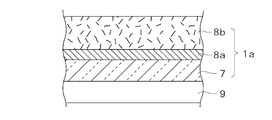
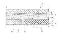
- the shield film 1 includes an insulating layer 7 that is a resin that has been polymerized until the degree of resin curing reaches 90% or more, a metal layer 8a as a shield layer laminated on the insulating layer, a metal And an adhesive layer 8b laminated on the layer 8a.
- the resin curing degree indicates the degree of progress of the resin curing reaction (reaction rate).
- the degree of resin curing is 0% for unreacted material and 100% for post-reaction material.
- the resin curing degree can be obtained from, for example, a measured value of the resin curing degree by an FT-IR (Fourier transform infrared spectroscopy) spectrum, and the target resin is irradiated with infrared rays and transmitted or dispersed.
- FT-IR Fastier transform infrared spectroscopy
- the shield film 1 may be in a state of being attached to a protective member before the heat press process for a printed circuit board or the like.
- the insulating layer 7 is formed of a resin that has been polymerized until the degree of cure of the resin reaches 90% or more.
- the curing mode may be any of thermal curing, ultraviolet curing, electron beam curing, etc., as long as the polymerization proceeds and cures.
- the thermosetting resin include a phenol resin, an acrylic resin, an epoxy resin, a melamine resin, a silicone resin, and an acrylic modified silicone resin.
- the ultraviolet curable resin include epoxy acrylate resins, polyester acrylate resins, and methacrylate-modified products thereof.
- the insulating layer 7 is preferably formed of a heat-resistant resin, and for example, polyimide is preferably used. Thereby, it can endure multiple times or a long-time heating press. Further, it is more preferable to use a thermoplastic polyimide having a lower water absorption than polyimide. Thereby, the swelling of the insulating layer can be prevented in the reflow process to the shield printed wiring board.
- the insulating layer 7 is not limited to the above resin, and examples of the heat resistant resin include polypropylene, crosslinked polyethylene, polyester, polybenzimidazole, aramid, polyimideamide, polyetherimide, polyphenylene sulfide (PPS), and polyethylene naphthalate. A resin such as (PEN) may be used.
- the insulating layer 7 is preferably made of an insulating resin formed in a film shape. As a result, the insulating layer 7 easily expands and contracts, and therefore, even when a pressed printed wiring board is heated and pressed, the insulating layer 7 easily follows the concavo-convex shape, and is less likely to break.
- the insulating layer 7 is not limited to a film-like insulating resin, and may be a coating layer formed by coating an insulating resin on a film serving as a base. Even when the insulating layer 7 is such a coating layer, the film serving as the substrate can be peeled off at room temperature before hot pressing with the printed wiring board. Therefore, the shield film from which the protective layer has been peeled off before hot pressing. The process of peeling the protective layer from the shield printed wiring board after the heat pressing is not necessary.
- the lower limit of the thickness of the insulating layer 7 is preferably 2 ⁇ m, and more preferably 4 ⁇ m.
- the upper limit of the thickness of the insulating layer 7 is preferably 25 ⁇ m, more preferably 12 ⁇ m, and even more preferably 8 ⁇ m.
- the insulating layer 7 may be one in which a pigment for coloring is contained in the resin as described above. For example, carbon black etc. can be mentioned.
- the insulating layer 7 may have a matte outer surface.
- the mat treatment may be performed by any of emboss roll processing, kneading mat, chemical mat coating, sand blast processing, and the like.
- the insulating layer 7 is not limited to a single layer structure, and may have a multiple layer structure.
- a two-layer structure formed by sequentially coating a hard layer made of a resin excellent in wear resistance and blocking resistance and a soft layer made of a resin excellent in cushioning properties may be used.
- the metal layer 8a is preferably formed by rolling. Thereby, while the shield film 1 has favorable shape retentivity, it can make favorable the followable
- the metal layer 8a is not limited to this, but is a metal thin film formed by vacuum deposition, electrolytic plating, electroless plating, sputtering, electron beam deposition, vacuum deposition, CVD, metal organic, or the like. There may be. Moreover, the metal layer 8a may be a metal thin film formed by a special electrolytic plating method so that the crystal has a structure in which the crystal spreads in the plane direction, like the metal foil. Thereby, like shape rolling, favorable shape retainability can be obtained.
- Examples of the metal material for forming the metal layer 8a include nickel, copper, silver, tin, gold, palladium, aluminum, chromium, titanium, zinc, and an alloy including any one or more of these materials. it can.
- the material of the metal layer 8a is particularly preferably silver. Thereby, even if the layer thickness is thin, the shield characteristic can be ensured.
- the lower limit of the thickness of the metal layer 8a is preferably 0.01 ⁇ m, more preferably 0.1 ⁇ m, and the upper limit of the thickness of the metal layer 8a is preferably 18 ⁇ m, more preferably 12 ⁇ m, and still more preferably 6 ⁇ m. Further, the metal layer 8a is not limited to a single layer structure, and may have a multiple layer structure.
- the adhesive layer 8b is formed of a conductive adhesive formed by adding a conductive filler to an adhesive resin.
- the shield printed wiring board includes a base member on which a ground wiring pattern and a signal wiring pattern are formed, and an insulating film laminated on the base member and exposing at least a part of the ground wiring pattern. It is formed by attaching a shield film to a plate and heating and pressing it. Since the shield film 1 has the adhesive layer 8b on the bonding surface with the printed wiring board, the shield film 1 is embedded in a portion where the ground wiring pattern of the insulating film is exposed at the time of heat pressing.
- the adhesive layer 8b is not limited to being formed of a conductive adhesive, and may be formed of an adhesive resin having no conductivity.
- Adhesive resins include thermoplastic resins such as polystyrene, vinyl acetate, polyester, polyethylene, polypropylene, polyamide, rubber, and acrylic, phenolic, epoxy, urethane, melamine, and alkyd. It is composed of a thermosetting resin such as a system. When heat resistance is not particularly required, a polyester-based thermoplastic resin that is not restricted by storage conditions or the like is desirable. When heat resistance or better flexibility is required, a highly reliable epoxy resin is required. A thermosetting resin is desirable.
- Examples of the conductive filler include silver-coated copper filler obtained by silver-plating carbon, silver, copper, nickel, solder, aluminum, and copper powder, and fillers obtained by metal-plating resin balls, glass beads, or the like.
- a mixture of Silver is expensive, copper lacks heat resistance reliability, aluminum lacks moisture resistance reliability, and solder is difficult to obtain sufficient conductivity. It is preferable to use a silver-coated copper filler or nickel having high reliability.
- an anisotropic conductive adhesive with a reduced amount of conductive filler may be used as the conductive adhesive.
- the film becomes thinner than the isotropic conductive adhesive, and the amount of the conductive filler is small. Can do.
- an isotropic conductive adhesive can also be used as a conductive adhesive.
- the ground connection to the ground circuit or the like can be achieved and the electromagnetic wave shield only by providing the conductive adhesive layer with the isotropic conductive adhesive. Since an effect can be given, it can serve as a shield layer and an adhesive layer. In this case, the metal layer may be omitted.
- the blending ratio of the conductive filler such as a metal filler to the adhesive resin depends on the shape of the filler, etc., but it is 100 parts by weight of the adhesive resin.
- the lower limit is preferably 10 parts by weight
- the upper limit is preferably 400 parts by weight.
- the blending ratio of the conductive filler to the adhesive resin is preferably 10 parts by weight with respect to 100 parts by weight of the adhesive resin.
- the upper limit is preferably 180 parts by weight.
- the blending ratio of the conductive filler to the adhesive resin is preferably 150 parts by weight with respect to 100 parts by weight of the adhesive resin.
- the upper limit is preferably 250 parts by weight.
- the lower limit is preferably 10 parts by weight, more preferably 20 parts by weight with respect to 100 parts by weight of the adhesive resin.
- the upper limit is preferably 400 parts by weight, and more preferably 150 parts by weight. If the silver-coated copper filler is used in excess of 400 parts by weight, the adhesion to the ground circuit is lowered and the flexibility of the shield film 1 is deteriorated.
- the amount is less than 10 parts by weight, the conductivity is significantly lowered.
- the lower limit is preferably 40 parts by weight, more preferably 100 parts by weight with respect to 100 parts by weight of the adhesive resin.
- the upper limit is preferably 400 parts by weight, more preferably 350 parts by weight.
- the nickel filler is used and exceeds 400 parts by weight, the adhesion to the ground circuit is lowered and the flexibility of the shield film 1 is deteriorated.
- the amount is less than 40 parts by weight, the conductivity is remarkably lowered.
- the shape of the conductive filler such as a metal filler may be any of a spherical shape, a needle shape, a fiber shape, a flake shape, and a dendritic shape.
- the thickness of the adhesive layer 8b is preferably 3 to 25 ⁇ m regardless of whether or not a conductive adhesive is used.
- the present invention is not limited to this, and the adhesive layer 8b may be thickened by mixing conductive fillers such as metal fillers. Moreover, when not mixing a conductive filler, it becomes possible to make it thin.
- the protective film 1 since the shield film 1 is formed of a resin that has been polymerized until the degree of resin curing reaches 90% or more, the protective film 1 has a conventional protective layer, such as a function as a base when laminating conductive layers. It has the function of. Therefore, since it is possible to form the shield film 1 that does not have a protective layer, it is possible to eliminate the step of peeling the protective layer from the shield film of the shield printed wiring board after the heat press step, which reduces the cost. Can be reduced. In addition, since a protective layer that is generally thicker than the combined thickness of the insulating layer, shield layer, and adhesive layer and is formed to about 50 ⁇ m is unnecessary, the shield film is wound and stored or transported. Cost reduction.
- the insulating layer 7 which is a resin that has been polymerized until the degree of resin cure reaches 90% or more, the metal layer 8a laminated on the insulating layer 7, and the adhesive laminated on the metal layer 8a.
- a shield film 1 having a layer 8b is formed.
- the insulating layer 7 is preferably a film-like resin, but even when formed by coating, since the insulating layer 7 is in a cured state, the film used as a substrate during coating is peeled off at room temperature before hot pressing. Is possible.
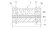
- a method for cutting the shield film 1 into a desired shape will be described. Specifically, as shown in FIG. 2, a laminated body 1 a having a laminated structure of shield films before being cut into a desired shape is laminated on the protective member 9.
- the laminated body 1 a is laminated so that the surface on the insulating layer 7 side comes into contact with the protective member 9, but is not limited thereto, and is laminated so that the surface on the adhesive layer 8 b side comes into contact with the protective member 9. May be.
- a release agent release agent
- the cutter 11 is used to perform a half cut that cuts the laminated body 1a while leaving the protective member 9 from the adhesive layer 8b side. That is, the cutter 11 cuts from the adhesive layer 8 b side to the middle of the protective member 9. Thereby, on the protection member 9, it is cut
- the peeling part 1b peels and the shield film 1 cut
- a plurality of shield films 1 can be laminated on the protective member 9.
- the process of cutting the shield film 1 into a desired shape is not limited to this.
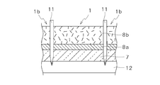
- the laminated body 1a is fixedly placed on the sheet 12 so that the surface on the insulating layer 7 side of the laminated body 1a is in contact with a protective sheet 12 made of sheet-like rubber, resin, or the like. May be cut into a desired shape by the cutter 11 to obtain the shield film 1.
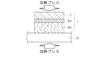
- the shield film 1 is peeled from the protective member 9 (see FIG. 4) on which the shield film 1 is laminated and placed at a desired position on the printed circuit board 5.
- a shield printed wiring board 10 as shown in FIG. 7 is manufactured.
- the shield film 1 is heat-pressed in a state where the insulating layer 7 is exposed, the insulating layer 7 is preferably formed of a heat resistant resin.
- the insulating layer is formed of a resin that has been polymerized until the resin curing degree is 90% or more. Therefore, since the insulating layer has the function of a conventional protective layer, the shield film 1 can be made to have no protective layer for protecting the insulating layer before heat pressing with the printed wiring board. In addition, since it is not necessary to protect the insulating layer even during hot pressing, the hot pressing step can be performed without stacking the protective layer. As a result, it is possible to eliminate the step of peeling the protective layer from the shield film of the shield printed wiring board after the hot pressing step, and the cost can be reduced.
- the shield printed wiring board 10 includes a base member 2 on which a wiring pattern 3 (ground wiring pattern 3b and signal wiring pattern 3a) is formed, and is laminated on the base member 2 and at least a part of the ground wiring pattern 3b.
- the shield film 1 is bonded to the printed circuit board 5 having the (non-insulating part 3 c) and the insulating film 4 exposed by the insulating removing part 4 a, and is heated and pressed. Since the shield film 1 has a conductive adhesive layer 8b on the surface to be bonded to the printed circuit board 5, the shield film 1 is embedded in a portion where the ground wiring pattern 3b of the insulating film 4 is exposed during heat pressing. Thereby, the non-insulating part 3c of the ground wiring pattern 3b and the metal layer 8a as the shield layer are electrically connected, and the shield film electromagnetic wave shielding function is further improved.
- the shield film 1 does not have a protective layer that is generally thicker than the combined thickness of the insulating layer, the shield layer, and the adhesive layer, the shield film 1 is formed to be more than half thinner than before. Become. Therefore, the shield film 1 becomes easy to follow the unevenness of the printed circuit board 5 and the insulation removal part 4a at the time of hot pressing. That is, in the shield printed wiring board 10, since the adhesive layer 8b of the shield film 1 follows along the unevenness of the printed circuit board 5 and also follows the insulation removal portion 4a, the insulation removal portion 4a and the adhesive layer 8b It is possible to prevent the generation of voids on the bonding surface. Therefore, by using the shield film 1, the embedding property of the adhesive layer 8b in the printed circuit board 5 in the shield printed wiring board 10 can be improved.
Landscapes
- Engineering & Computer Science (AREA)
- Microelectronics & Electronic Packaging (AREA)
- Manufacturing & Machinery (AREA)
- Physics & Mathematics (AREA)
- Electromagnetism (AREA)
- Shielding Devices Or Components To Electric Or Magnetic Fields (AREA)
- Laminated Bodies (AREA)
- Structure Of Printed Boards (AREA)
Priority Applications (5)
| Application Number | Priority Date | Filing Date | Title |
|---|---|---|---|
| KR1020157016438A KR20150096679A (ko) | 2012-12-20 | 2013-12-10 | 실드 프린트 배선판의 제조 방법, 실드 필름 및 실드 프린트 배선판 |
| CN201380067307.7A CN104871651A (zh) | 2012-12-20 | 2013-12-10 | 屏蔽印刷线路板的制造方法、屏蔽膜及屏蔽印刷线路板 |
| US14/653,917 US20150373835A1 (en) | 2012-12-20 | 2013-12-10 | Method for manufacturing shield printed wiring board, and shield film and shield printed wiring board |
| HK16102067.6A HK1214463A1 (zh) | 2012-12-20 | 2013-12-10 | 屏蔽印刷线路板的制造方法、屏蔽膜及屏蔽印刷线路板 |
| US15/145,127 US20160249446A1 (en) | 2012-12-20 | 2016-05-03 | Method for manufacturing shield printed wiring board, and shield film and shield printed wiring board |
Applications Claiming Priority (2)
| Application Number | Priority Date | Filing Date | Title |
|---|---|---|---|
| JP2012-278551 | 2012-12-20 | ||
| JP2012278551A JP2014123630A (ja) | 2012-12-20 | 2012-12-20 | シールドプリント配線板の製造方法、シールドフィルム、及び、シールドプリント配線板 |
Related Child Applications (2)
| Application Number | Title | Priority Date | Filing Date |
|---|---|---|---|
| US14/653,917 A-371-Of-International US20150373835A1 (en) | 2012-12-20 | 2013-12-10 | Method for manufacturing shield printed wiring board, and shield film and shield printed wiring board |
| US15/145,127 Continuation US20160249446A1 (en) | 2012-12-20 | 2016-05-03 | Method for manufacturing shield printed wiring board, and shield film and shield printed wiring board |
Publications (1)
| Publication Number | Publication Date |
|---|---|
| WO2014097933A1 true WO2014097933A1 (ja) | 2014-06-26 |
Family
ID=50978268
Family Applications (1)
| Application Number | Title | Priority Date | Filing Date |
|---|---|---|---|
| PCT/JP2013/083119 WO2014097933A1 (ja) | 2012-12-20 | 2013-12-10 | シールドプリント配線板の製造方法、シールドフィルム、及び、シールドプリント配線板 |
Country Status (7)
Families Citing this family (9)
| Publication number | Priority date | Publication date | Assignee | Title |
|---|---|---|---|---|
| JP2016058565A (ja) * | 2014-09-10 | 2016-04-21 | 住友ベークライト株式会社 | 電磁波シールド用フィルム |
| JP6402584B2 (ja) * | 2014-10-23 | 2018-10-10 | 住友ベークライト株式会社 | 電磁波シールド用フィルムの製造方法 |
| CN105139922A (zh) * | 2015-09-21 | 2015-12-09 | 杨天纬 | 一种用于线缆的屏蔽膜及制造方法及线材的制造方法 |
| JP6709669B2 (ja) * | 2016-04-20 | 2020-06-17 | 信越ポリマー株式会社 | 電磁波シールドフィルムおよび電磁波シールドフィルム付きプリント配線板 |
| KR102467723B1 (ko) * | 2017-02-13 | 2022-11-16 | 타츠타 전선 주식회사 | 그라운드 부재, 차폐 프린트 배선판 및 차폐 프린트 배선판의 제조 방법 |
| TWI813823B (zh) * | 2018-12-03 | 2023-09-01 | 日商拓自達電線股份有限公司 | 接地構件及遮蔽印刷配線板 |
| WO2020122166A1 (ja) * | 2018-12-12 | 2020-06-18 | タツタ電線株式会社 | シールドプリント配線板及びシールドプリント配線板の製造方法 |
| TWI741648B (zh) * | 2020-06-12 | 2021-10-01 | 亞洲電材股份有限公司 | 覆蓋膜及其製備方法 |
| CN113613482B (zh) * | 2021-08-06 | 2024-03-19 | 航天智造科技股份有限公司 | 适用于极小接地孔接地的电磁波屏蔽膜、制备方法及应用 |
Citations (6)
| Publication number | Priority date | Publication date | Assignee | Title |
|---|---|---|---|---|
| JP2005056906A (ja) * | 2003-08-05 | 2005-03-03 | Reiko Co Ltd | 電磁波遮蔽性転写フイルム |
| JP2009038278A (ja) * | 2007-08-03 | 2009-02-19 | Tatsuta System Electronics Kk | プリント配線板用シールドフィルム及びプリント配線板 |
| JP2009246121A (ja) * | 2008-03-31 | 2009-10-22 | Nippon Steel Chem Co Ltd | 電磁波シールド材及びその製造方法 |
| JP2010238870A (ja) * | 2009-03-31 | 2010-10-21 | Toyo Ink Mfg Co Ltd | 電磁波シールド性カバーレイフィルム、フレキシブルプリント配線板の製造方法、及びフレキシブルプリント配線板。 |
| JP2012015311A (ja) * | 2010-06-30 | 2012-01-19 | Sony Chemical & Information Device Corp | シールドフィルム及びシールド配線板 |
| JP2012169412A (ja) * | 2011-02-14 | 2012-09-06 | Nippon Steel Chem Co Ltd | 回路基板 |
Family Cites Families (6)
| Publication number | Priority date | Publication date | Assignee | Title |
|---|---|---|---|---|
| JP3498386B2 (ja) * | 1994-10-19 | 2004-02-16 | 住友電気工業株式会社 | シールド付きフレキシブル配線板及びその製造方法 |
| JP4170781B2 (ja) * | 2003-01-17 | 2008-10-22 | 松下電器産業株式会社 | 基板の製造方法 |
| JP4319167B2 (ja) * | 2005-05-13 | 2009-08-26 | タツタ システム・エレクトロニクス株式会社 | シールドフィルム、シールドプリント配線板、シールドフレキシブルプリント配線板、シールドフィルムの製造方法及びシールドプリント配線板の製造方法 |
| KR101457528B1 (ko) * | 2008-05-15 | 2014-11-04 | 삼성디스플레이 주식회사 | 임프린트 기판의 제조방법 및 임프린팅 방법 |
| JP5521227B2 (ja) * | 2009-01-26 | 2014-06-11 | タツタ電線株式会社 | 導電性粘着シート及びそれを備えた電磁波シールド材、プリント配線板 |
| JP2011171522A (ja) * | 2010-02-19 | 2011-09-01 | Toyo Ink Sc Holdings Co Ltd | 硬化性電磁波シールド性接着性フィルムおよびその製造方法 |
-
2012
- 2012-12-20 JP JP2012278551A patent/JP2014123630A/ja active Pending
-
2013
- 2013-12-10 CN CN201380067307.7A patent/CN104871651A/zh active Pending
- 2013-12-10 US US14/653,917 patent/US20150373835A1/en not_active Abandoned
- 2013-12-10 WO PCT/JP2013/083119 patent/WO2014097933A1/ja active Application Filing
- 2013-12-10 KR KR1020157016438A patent/KR20150096679A/ko not_active Ceased
- 2013-12-10 HK HK16102067.6A patent/HK1214463A1/zh unknown
- 2013-12-16 TW TW102146399A patent/TWI627883B/zh active
-
2016
- 2016-05-03 US US15/145,127 patent/US20160249446A1/en not_active Abandoned
Patent Citations (6)
| Publication number | Priority date | Publication date | Assignee | Title |
|---|---|---|---|---|
| JP2005056906A (ja) * | 2003-08-05 | 2005-03-03 | Reiko Co Ltd | 電磁波遮蔽性転写フイルム |
| JP2009038278A (ja) * | 2007-08-03 | 2009-02-19 | Tatsuta System Electronics Kk | プリント配線板用シールドフィルム及びプリント配線板 |
| JP2009246121A (ja) * | 2008-03-31 | 2009-10-22 | Nippon Steel Chem Co Ltd | 電磁波シールド材及びその製造方法 |
| JP2010238870A (ja) * | 2009-03-31 | 2010-10-21 | Toyo Ink Mfg Co Ltd | 電磁波シールド性カバーレイフィルム、フレキシブルプリント配線板の製造方法、及びフレキシブルプリント配線板。 |
| JP2012015311A (ja) * | 2010-06-30 | 2012-01-19 | Sony Chemical & Information Device Corp | シールドフィルム及びシールド配線板 |
| JP2012169412A (ja) * | 2011-02-14 | 2012-09-06 | Nippon Steel Chem Co Ltd | 回路基板 |
Also Published As
| Publication number | Publication date |
|---|---|
| US20160249446A1 (en) | 2016-08-25 |
| TWI627883B (zh) | 2018-06-21 |
| KR20150096679A (ko) | 2015-08-25 |
| TW201440589A (zh) | 2014-10-16 |
| HK1214463A1 (zh) | 2016-07-22 |
| CN104871651A (zh) | 2015-08-26 |
| JP2014123630A (ja) | 2014-07-03 |
| US20150373835A1 (en) | 2015-12-24 |
Similar Documents
| Publication | Publication Date | Title |
|---|---|---|
| WO2014097933A1 (ja) | シールドプリント配線板の製造方法、シールドフィルム、及び、シールドプリント配線板 | |
| TWI734930B (zh) | 電磁波屏蔽膜 | |
| JP2016029748A (ja) | シールドプリント配線板の製造方法 | |
| JP7256618B2 (ja) | 転写フィルム付電磁波シールドフィルム、転写フィルム付電磁波シールドフィルムの製造方法及びシールドプリント配線板の製造方法 | |
| CN104797420B (zh) | 层叠膜和屏蔽印刷布线板 | |
| KR20160013048A (ko) | 전자파 실드 필름, 이것을 사용한 프린트 배선판, 및 압연 동박 | |
| CN105684566A (zh) | 屏蔽壳体、印刷线路板、电子设备及屏蔽壳体的制作方法 | |
| JP4360774B2 (ja) | 補強シールドフィルム及びシールドフレキシブルプリント配線板 | |
| JP7023836B2 (ja) | 電磁波シールドフィルム | |
| JP2023072062A (ja) | シールドプリント配線板 | |
| JP7027618B2 (ja) | 電磁波シールドフィルム | |
| JP6956926B1 (ja) | 電磁波シールドフィルム | |
| JP2019065069A (ja) | 導電性接着剤シート | |
| TWI754611B (zh) | Fpc用導電性黏著片材及使用此片材之fpc | |
| KR102790802B1 (ko) | 전자파 차폐 필름 | |
| JP6731393B2 (ja) | 電磁波シールドフィルム | |
| KR101411978B1 (ko) | 금속화 고분자필름에 착색층이 형성된 전자파 차폐용 접착테이프의 제조방법 및 그에 의한 접착테이프 | |
| JP7595410B2 (ja) | 電磁波シールドフィルム及び回路基板 | |
| TWI725334B (zh) | 連接用膜、屏蔽印刷配線板之製造方法及屏蔽印刷配線板 | |
| TWI829973B (zh) | 電磁波屏蔽膜 | |
| JP2021019012A (ja) | 電磁波シールドフィルム、回路基板、及び回路基板の製造方法 | |
| KR102843954B1 (ko) | 자성 시트 | |
| HK40041175A (en) | Method for manufacturing shielded printed wiring board and shielded printed wiring board | |
| JP2021061365A (ja) | 電磁波シールドフィルム、回路基板、及び回路基板の製造方法 | |
| JP2012195619A (ja) | フレックスリジッドプリント配線板 |
Legal Events
| Date | Code | Title | Description |
|---|---|---|---|
| 121 | Ep: the epo has been informed by wipo that ep was designated in this application |
Ref document number: 13863802 Country of ref document: EP Kind code of ref document: A1 |
|
| ENP | Entry into the national phase |
Ref document number: 20157016438 Country of ref document: KR Kind code of ref document: A |
|
| WWE | Wipo information: entry into national phase |
Ref document number: 14653917 Country of ref document: US |
|
| NENP | Non-entry into the national phase |
Ref country code: DE |
|
| 122 | Ep: pct application non-entry in european phase |
Ref document number: 13863802 Country of ref document: EP Kind code of ref document: A1 |