WO2014097710A1 - Structure de fixation pour fibre optique, module laser à semi-conducteurs, et procédé de fixation pour fibre optique - Google Patents
Structure de fixation pour fibre optique, module laser à semi-conducteurs, et procédé de fixation pour fibre optique Download PDFInfo
- Publication number
- WO2014097710A1 WO2014097710A1 PCT/JP2013/077242 JP2013077242W WO2014097710A1 WO 2014097710 A1 WO2014097710 A1 WO 2014097710A1 JP 2013077242 W JP2013077242 W JP 2013077242W WO 2014097710 A1 WO2014097710 A1 WO 2014097710A1
- Authority
- WO
- WIPO (PCT)
- Prior art keywords
- optical fiber
- fixing
- groove
- fixed
- semiconductor laser
- Prior art date
Links
Images


Classifications
-
- G—PHYSICS
- G02—OPTICS
- G02B—OPTICAL ELEMENTS, SYSTEMS OR APPARATUS
- G02B6/00—Light guides; Structural details of arrangements comprising light guides and other optical elements, e.g. couplings
- G02B6/24—Coupling light guides
- G02B6/42—Coupling light guides with opto-electronic elements
- G02B6/4201—Packages, e.g. shape, construction, internal or external details
- G02B6/4219—Mechanical fixtures for holding or positioning the elements relative to each other in the couplings; Alignment methods for the elements, e.g. measuring or observing methods especially used therefor
- G02B6/4236—Fixing or mounting methods of the aligned elements
- G02B6/4239—Adhesive bonding; Encapsulation with polymer material
-
- G—PHYSICS
- G02—OPTICS
- G02B—OPTICAL ELEMENTS, SYSTEMS OR APPARATUS
- G02B6/00—Light guides; Structural details of arrangements comprising light guides and other optical elements, e.g. couplings
- G02B6/24—Coupling light guides
- G02B6/42—Coupling light guides with opto-electronic elements
- G02B6/4201—Packages, e.g. shape, construction, internal or external details
- G02B6/4219—Mechanical fixtures for holding or positioning the elements relative to each other in the couplings; Alignment methods for the elements, e.g. measuring or observing methods especially used therefor
- G02B6/4236—Fixing or mounting methods of the aligned elements
- G02B6/424—Mounting of the optical light guide
- G02B6/4243—Mounting of the optical light guide into a groove
-
- G—PHYSICS
- G02—OPTICS
- G02B—OPTICAL ELEMENTS, SYSTEMS OR APPARATUS
- G02B6/00—Light guides; Structural details of arrangements comprising light guides and other optical elements, e.g. couplings
- G02B6/24—Coupling light guides
- G02B6/42—Coupling light guides with opto-electronic elements
- G02B6/4201—Packages, e.g. shape, construction, internal or external details
- G02B6/4256—Details of housings
- G02B6/4257—Details of housings having a supporting carrier or a mounting substrate or a mounting plate
-
- H—ELECTRICITY
- H01—ELECTRIC ELEMENTS
- H01S—DEVICES USING THE PROCESS OF LIGHT AMPLIFICATION BY STIMULATED EMISSION OF RADIATION [LASER] TO AMPLIFY OR GENERATE LIGHT; DEVICES USING STIMULATED EMISSION OF ELECTROMAGNETIC RADIATION IN WAVE RANGES OTHER THAN OPTICAL
- H01S5/00—Semiconductor lasers
- H01S5/02—Structural details or components not essential to laser action
- H01S5/022—Mountings; Housings
- H01S5/0225—Out-coupling of light
- H01S5/02251—Out-coupling of light using optical fibres
-
- G—PHYSICS
- G02—OPTICS
- G02B—OPTICAL ELEMENTS, SYSTEMS OR APPARATUS
- G02B6/00—Light guides; Structural details of arrangements comprising light guides and other optical elements, e.g. couplings
- G02B6/24—Coupling light guides
- G02B6/42—Coupling light guides with opto-electronic elements
- G02B6/4201—Packages, e.g. shape, construction, internal or external details
- G02B6/4202—Packages, e.g. shape, construction, internal or external details for coupling an active element with fibres without intermediate optical elements, e.g. fibres with plane ends, fibres with shaped ends, bundles
- G02B6/4203—Optical features
-
- G—PHYSICS
- G02—OPTICS
- G02B—OPTICAL ELEMENTS, SYSTEMS OR APPARATUS
- G02B6/00—Light guides; Structural details of arrangements comprising light guides and other optical elements, e.g. couplings
- G02B6/24—Coupling light guides
- G02B6/42—Coupling light guides with opto-electronic elements
- G02B6/4201—Packages, e.g. shape, construction, internal or external details
- G02B6/4204—Packages, e.g. shape, construction, internal or external details the coupling comprising intermediate optical elements, e.g. lenses, holograms
- G02B6/4207—Packages, e.g. shape, construction, internal or external details the coupling comprising intermediate optical elements, e.g. lenses, holograms with optical elements reducing the sensitivity to optical feedback
- G02B6/4208—Packages, e.g. shape, construction, internal or external details the coupling comprising intermediate optical elements, e.g. lenses, holograms with optical elements reducing the sensitivity to optical feedback using non-reciprocal elements or birefringent plates, i.e. quasi-isolators
-
- H—ELECTRICITY
- H01—ELECTRIC ELEMENTS
- H01S—DEVICES USING THE PROCESS OF LIGHT AMPLIFICATION BY STIMULATED EMISSION OF RADIATION [LASER] TO AMPLIFY OR GENERATE LIGHT; DEVICES USING STIMULATED EMISSION OF ELECTROMAGNETIC RADIATION IN WAVE RANGES OTHER THAN OPTICAL
- H01S5/00—Semiconductor lasers
- H01S5/005—Optical components external to the laser cavity, specially adapted therefor, e.g. for homogenisation or merging of the beams or for manipulating laser pulses, e.g. pulse shaping
- H01S5/0064—Anti-reflection components, e.g. optical isolators
-
- H—ELECTRICITY
- H01—ELECTRIC ELEMENTS
- H01S—DEVICES USING THE PROCESS OF LIGHT AMPLIFICATION BY STIMULATED EMISSION OF RADIATION [LASER] TO AMPLIFY OR GENERATE LIGHT; DEVICES USING STIMULATED EMISSION OF ELECTROMAGNETIC RADIATION IN WAVE RANGES OTHER THAN OPTICAL
- H01S5/00—Semiconductor lasers
- H01S5/02—Structural details or components not essential to laser action
- H01S5/022—Mountings; Housings
- H01S5/0225—Out-coupling of light
- H01S5/02253—Out-coupling of light using lenses
-
- H—ELECTRICITY
- H01—ELECTRIC ELEMENTS
- H01S—DEVICES USING THE PROCESS OF LIGHT AMPLIFICATION BY STIMULATED EMISSION OF RADIATION [LASER] TO AMPLIFY OR GENERATE LIGHT; DEVICES USING STIMULATED EMISSION OF ELECTROMAGNETIC RADIATION IN WAVE RANGES OTHER THAN OPTICAL
- H01S5/00—Semiconductor lasers
- H01S5/02—Structural details or components not essential to laser action
- H01S5/022—Mountings; Housings
- H01S5/023—Mount members, e.g. sub-mount members
- H01S5/02325—Mechanically integrated components on mount members or optical micro-benches
- H01S5/02326—Arrangements for relative positioning of laser diodes and optical components, e.g. grooves in the mount to fix optical fibres or lenses
Definitions
- the present invention relates to an optical fiber fixing structure, a semiconductor laser module, and an optical fiber fixing method capable of preventing the optical fiber from being displaced and stably fixing the optical fiber.
- a laser diode (semiconductor laser) chip and an optical fiber are optically connected.
- the optical fiber is aligned on the optical axis with the semiconductor laser and then fixed on the pedestal with solder, an adhesive, or the like.
- FIG. 10 is a schematic view showing a conventional semiconductor laser module 100.
- a semiconductor laser pedestal 105 and a fiber fixing pedestal 109 are arranged in alignment on a base 103.
- a semiconductor laser 107 is fixed on the semiconductor laser pedestal 105.
- An optical fiber 113 is fixed to the fiber fixing base 109 with an adhesive 111 or the like. In this state, the optical fiber 113 and the semiconductor laser 107 are optically coupled.
- the fixing structure between the optical fiber and the fiber fixing base is referred to as an optical fiber fixing structure.
- FIG. 11 is a view showing the optical fiber fixing structure 110 in the semiconductor laser module 100
- FIG. 11 (a) is a side view
- FIG. 11 (b) is a front view.
- an adhesive 111 is provided on the fiber fixing base 109 having a flat upper surface so as to rise upward due to surface tension, and the optical fiber 113 is fixed by the adhesive 111.
- the optical fiber fixing structure 110 is fixed to the fiber fixing base 109 only under the optical fiber 113. That is, only one side of the optical fiber 113 is fixed to the fiber fixing base 109. In this case, when a force is applied in the axial direction on the rear side of the fixed portion of the optical fiber 113 (in the direction of arrow G in the figure), the rotational direction shifts so that the tip of the optical fiber 113 is shifted up and down (in the figure). Arrow H direction).
- Such an optical fiber misalignment becomes a serious problem particularly in the case of a single mode lensed fiber. That is, in a semiconductor laser module using an optical coupling system with a particularly narrow coupling tolerance, such as a single mode lensed fiber, such a positional shift causes an optical coupling state between the semiconductor laser and the optical fiber. There was a problem that the fiber end output of the semiconductor laser module deteriorated due to the deviation.
- a wedged fiber having a wedge-shaped tip such as an optical fiber used for optical coupling with a semiconductor laser having a wavelength band of about 980 nm
- the vertical direction of the optical coupling characteristic is used. Since the optical coupling tolerance is extremely narrow, the degradation of the fiber end output has become an even greater problem.
- Patent Document 1 there is a method in which a groove or hole is provided in the fiber fixing base, and the optical fiber 113 is fixed to the fiber fixing base by filling the groove or hole with an adhesive in a state where the optical fiber 113 is disposed in the groove or hole.
- FIG. 12A is a view showing an optical fiber fixing structure 110a using a fiber fixing base 109a having a groove having a substantially rectangular cross section.
- the optical fiber 113 is disposed in a groove formed in the fiber fixing base 109a, and the optical fiber 113 is fixed to the fiber fixing base 109a by an adhesive 111 filled in the groove.
- the optical fiber 113 is fixed to the fiber fixing base 109a in the three directions of right and left and lower with respect to the rectangular groove. Due to the contraction of the optical fiber 113, the optical fiber 113 is stressed downward and in the left-right direction (in the direction of arrow J in the figure). Therefore, the tip position of the optical fiber 113 may be shifted when the adhesive is cured.
- FIG. 12B is a view showing an optical fiber fixing structure 110b using a fiber fixing base 109b having a circular hole.
- the optical fiber 113 is inserted into a hole formed in the fiber fixing base 109b, and the optical fiber 113 is fixed to the fiber fixing base 109b with an adhesive 111 filled in the hole.
- the optical fiber fixing structure 110b when the adhesive 111 is cured and contracted, the optical fiber 113 in the hole receives substantially uniform stress in all directions (in the direction of arrow K in the figure). However, when the adhesive 111 is cured and contracted, the surface of the optical fiber 113 is pulled in all directions, and compressive stress is applied. Further, the temperature change after bonding causes expansion and contraction of the adhesive, and compressive or tensile stress is applied to the entire circumference of the optical fiber 113. In such a case, since the entire circumference of the adhesive is regulated by the holes, the stress cannot be released, and the adhesive 111 is peeled off from the surface of the fiber fixing base 109b or the optical fiber 113, or on the surface of the fiber fixing base 109b. There is a risk of cracking.
- the present invention has been made in view of such a problem, and an object of the present invention is to provide an optical fiber fixing structure or the like that can prevent the positional deviation of the optical fiber and can stably fix the optical fiber.
- a first invention is an optical fiber fixing structure, comprising a pedestal and an optical fiber fixed to the pedestal with a fixing member, and the pedestal includes the optical fiber.
- a groove is formed along the axial direction of the optical fiber, and the optical fiber is fixed to the mutually facing fixed surfaces of the inner surface of the groove by the fixing member, and when viewed from the axial direction of the optical fiber, the optical fiber and the optical fiber
- a space structure in which the optical fiber is not fixed to the base is formed in both directions substantially perpendicular to the fixing direction with the fixing surface.
- the groove is formed on an upper surface of the pedestal, the optical fiber is fixed to the fixing surface which is an inner surface of the groove by the fixing member, and the optical fiber is fixed to the bottom side of the groove.
- An interval changing portion in which the interval is different from the interval between the fixed surfaces in the part may be formed.
- a plurality of the grooves are provided in the axial direction of the optical fiber, and the length of the groove near the tip of the optical fiber may be shorter than the length of the groove far from the tip of the optical fiber. Good.
- the optical fiber is fixed by the fixing member only to one facing surface of the groove formed in the pedestal.
- a space portion in which the base and the optical fiber are not fixed is formed in a direction perpendicular to the fixing direction of the optical fiber. For this reason, the force by shrinkage
- a plurality of grooves are formed in the axial direction of the optical fiber, and the optical fiber can be fixed to the pedestal with higher accuracy by dividing the optical fiber into a short groove on the tip side and the other long groove.
- the amount of adhesive used is small, so that it is possible to suppress the influence of misalignment due to the adhesive.
- a sufficient amount of fixing strength cannot be obtained with a small amount of adhesive, it is possible to secure the sufficient fixing strength by fixing the optical fiber with the long groove.
- a second invention has an optical fiber fixing structure according to the first invention, and includes a base, the optical fiber fixing structure provided on the base, and the optical fiber and light in the optical fiber fixing structure. And a semiconductor laser connected to the semiconductor laser module.
- a lens and an isolator may be provided between the semiconductor laser and the optical fiber.
- the second invention it is possible to obtain a semiconductor laser module in which the optical coupling state between the optical fiber and the semiconductor laser is small and the fiber end output is less deteriorated.
- a third invention is an optical fiber fixing method, wherein the optical fiber is disposed in the groove of a pedestal having a groove, and the optical fiber and an inner surface of the groove are opposed to each other. And applying the fixing member; and curing the fixing member to fix the optical fiber to the pedestal.
- the optical fiber viewed from the axial direction of the optical fiber, In the optical fiber fixing method, the optical fiber is fixed so as to form a space portion in which the optical fiber is not fixed to the base in both directions substantially perpendicular to the fixing direction of the fiber and the fixing surface.
- the length of the first groove near the tip of the optical fiber is shorter than the length of the second groove far from the tip of the optical fiber, and is between the optical fiber and the fixed surface of the first groove.
- the third invention it is possible to easily obtain a semiconductor laser module in which the optical coupling state between the optical fiber and the semiconductor laser is small and the fiber end output is less deteriorated.
- the optical fiber is fixed in a short groove, so it is possible to fix the position close to the tip of the optical fiber with a small amount of adhesive, It is possible to suppress the influence of positional deviation due to the adhesive. Further, since the optical fiber is fixed by the long groove after the fixing to the short groove is completed, sufficient fixing strength can be ensured.
- an optical fiber fixing structure or the like that can prevent the positional deviation of the optical fiber and can stably fix the optical fiber.
- FIG. 1A is a view showing a semiconductor laser module 1
- FIG. 1B is a view showing a modification thereof.
- 3A is a view showing the optical fiber fixing structure 10
- FIG. 3B is an enlarged view of a portion A in FIG. 3A.
- FIGS. 4A to 4C are views showing optical fiber fixing structures 10a, 10b, and 10c having interval changing portions 21a, 21b, and 21c, respectively.
- the figure which shows the semiconductor laser module 1a The figure which shows the semiconductor laser module 1b.
- FIG. 8A is a diagram showing the semiconductor laser module 1c
- FIG. 8B is a diagram showing the semiconductor laser module 1d.
- FIG. 11A is a side view showing a conventional optical fiber fixing structure 110
- FIG. 11B is a front view thereof
- 12A is a front view showing a conventional optical fiber fixing structure 110a
- FIG. 12B is a front view showing a conventional optical fiber fixing structure 110b.
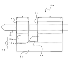
- FIG. 1A is a perspective view of the semiconductor laser module 1.
- the semiconductor laser module 1 mainly includes a base 3, a semiconductor laser base 5, a semiconductor laser 7, a fiber fixing base 9, an optical fiber 13, and the like.
- the base 3 is a plate-like member in which each component is installed in the upper part.
- the base 3 for example, AlN, CuW, Al 2 O 3 or the like can be used, and it is desirable that the base 3 be made of a material having excellent thermal conductivity.
- the semiconductor laser pedestal 5 is fixed on the base 3 with solder or the like.
- the semiconductor laser pedestal 5 is a member to which the semiconductor laser 7 is fixed.
- the semiconductor laser pedestal 5 for example, AlN, CuW, Cu, Si or the like can be used, and the semiconductor laser 7 can emit a laser having a desired wavelength, for example, an InP laser or a GaAs laser.
- a GaAsAl laser or the like can be used.
- a fiber fixing base 9 is fixed on the base 3 with solder, an adhesive, or the like so as to be provided with the semiconductor laser base 5.
- the fiber fixing base 9 for example, a glass material such as borosilicate glass or quartz glass, AlN, CuW, Al 2 O 3 or the like can be used.
- the fiber fixing base 9 can be configured integrally with the base 3.
- the semiconductor laser base 5 and the fiber fixing base 9 may be integrally formed.
- the integrated pedestal is fixed to the base 3 with solder or the like.
- the base 3 is not necessarily required. In the following description, an example will be described in which the fiber fixing base 9 is formed separately from the base 3 and is bonded onto the base 3.
- An optical fiber 13 is fixed to the upper surface of the fiber fixing base 9 with an adhesive 11.
- the adhesive 11 for example, a UV curing system, a thermosetting system, a UV curing + thermosetting system, a room temperature standing curing system, or the like can be used. In this state, the optical fiber 13 and the semiconductor laser 7 are optically coupled.
- a fixing member for fixing the optical fiber 13 not the adhesive 11 but solder may be used. In this case, for example, AuSn, SnAgCu, SnBi or the like can be used as a solder material.
- solder the adhesive 11 is used as the fixing member and the adhesive 11 cures and shrinks will be described. However, in the case where solder is used, the same effect can be obtained for the solidification shrinkage of the solder. Can do.
- Alignment between the optical fiber 13 and the semiconductor laser 7 is performed, for example, by moving the optical fiber 13 relative to the semiconductor laser 7 in a state where light is incident on the optical fiber 13 from the semiconductor laser 7.
- the optical fiber 13 is moved by a hand (not shown) that chucks the optical fiber 13.
- Positioning is performed so that the light intensity detected by the light detector connected to the optical fiber 13 is maximized, and the positioning operation is completed in a state where a predetermined intensity or more is detected.
- the adhesive 11 is cured by irradiating the adhesive 11 with heat or ultraviolet rays.
- the optical fiber 13 is fixed on the fiber fixing base 9 at an appropriate position.
- FIG. 3 is a schematic view showing the optical fiber fixing structure 10, FIG. 3 (a) is a front view, and FIG. 3 (b) is an enlarged view of part A of FIG. 3 (a).
- the fiber fixing base 9 is provided with a groove 15 along the axial direction of the optical fiber 13 to be fixed.
- the groove 15 opens upward.
- the optical fiber 13 is disposed inside the groove 15 along the groove 15.
- the optical fiber 13 is fixed to the inner surface of the groove 15 with an adhesive 11.
- the inner surfaces of the grooves 15 facing each other serve as the fixing surface 17 of the optical fiber 13. That is, the optical fiber 13 is fixed by the adhesive 11 to the opposing fixed surface 17 that is the inner surface of the groove 15.
- a space 19 in which the adhesive 11 and the fiber fixing base 9 are not bonded is formed in the vertical direction of the optical fiber 13. That is, the space portion 19 is provided in the vertical direction substantially perpendicular to the fixing direction in which the optical fiber 13 is fixed.
- the width of the groove 15 (the distance between the fixing surfaces 17 in the fixing direction of the optical fiber 13 in the horizontal direction in FIG. 3B) is, for example, about 200 ⁇ m to 500 ⁇ m. If the width of the groove 15 is too large, the adhesive 11 tends to flow downward and may fill the space below. Further, if the width of the groove 15 is too narrow, the alignment width of the optical fiber 13 becomes narrow.
- the adhesive 11 is given a contraction force when it is cured.
- a force is a force from the surface of the adhesive 11 toward the fixing surface 17 (in the direction of arrow B in the figure).
- the optical fiber 13 is pulled in the direction of both the fixed surfaces 17. Accordingly, the force in the direction of the fixing surface 17 (left and right direction) is substantially canceled, and the positional deviation of the optical fiber 13 in the left and right direction when the adhesive 11 is cured and contracted can be suppressed.
- the vertical direction of the optical fiber 13 substantially the same force is applied in the vertical direction, and the optical fiber 13 is not pulled in one direction.
- the optical fiber 13 is fixed only to the opposing fixing surface 17 and the space portion 19 is provided in the direction perpendicular thereto, so that the optical fiber 13 and the fiber fixing base are disposed in the direction of the space portion 19. 9 is not joined. For this reason, when the adhesive agent 11 contracts, the stresses generated in the vertical direction and the horizontal direction are symmetrical, and the positional deviation of the optical fiber 13 can be suppressed.
- the depth of the groove 15 is sufficiently deep with respect to the width of the groove 15 (for example, the depth is 1.5 times or more of the width). This is because if the depth of the groove 15 is too shallow, the adhesive 11 flows and adheres to the bottom surface of the groove 15, making it difficult to form the space 19 appropriately.
- the viscosity of the adhesive 11 is preferably 10 to 200 Pa / s, for example, and more preferably 15 to 100 Pa / s. If the viscosity of the adhesive 11 is too low, the adhesive 11 tends to flow downward. Moreover, if the viscosity of the adhesive 11 is too high, alignment of the optical fiber 13 becomes difficult.
- Such adjustment of the viscosity can be adjusted by, for example, the filler content. When a large amount of filler is contained, the viscosity can be increased. Moreover, the shrinkage
- the width of the groove 15 differs depending on the position. Specifically, the lower groove width D is larger than the width C (interval between the fixing surfaces 17) of the fixing portion where the optical fiber 13 and the fiber fixing base 9 are fixed by the adhesive 11. That is, a step is formed in the lower portion of the fixed surface 17 by the interval changing portion 21a.
- the adhesive agent 11 flows below because the lower part of the fixed surface 17 to which the adhesive agent 11 was apply
- the optical fiber fixing structure 10b shown in FIG. the groove width below the optical fiber 13 and the fiber fixing base 9 is smaller than the width of the fixing portion (interval between the fixing surfaces 17) to which the optical fiber 13 and the fiber fixing base 9 are fixed. That is, a step is formed in the lower portion of the fixed surface 17 by the interval changing portion 21b. In this way, the adhesive 11 can be prevented from flowing downward from the fixed surface 17 by changing the interval regardless of the direction in which the step is formed.
- step difference is 0.1 mm or more, for example.
- the same effect can be obtained with the optical fiber fixing structure 10c shown in FIG.
- the lower portion of the fixing surface 17 is formed in a circular shape. Even in this case, the width of the groove changes in the lower portion of the fixed surface 17 by the interval changing portion 21c. As described above, if the changing portion of the width of the groove 15 is formed in the lower portion of the fixed surface 17, it is possible to prevent the adhesive 11 from flowing downward from the fixed surface 17 regardless of the form.
- the adhesive surface portion of the adhesive of the fixing surface 17 or the entire surface of the fixing surface 17 is processed into a ground glass shape to increase the surface roughness of the fixing surface 17, thereby increasing the surface tension effect of the adhesive. It is possible to prevent the adhesive from flowing downward.
- the surface roughness of the fixed surface 17 is preferably 0.8 ⁇ m to 25.0 ⁇ m, more preferably 1.0 ⁇ m to 12.5 ⁇ m, in terms of centerline average roughness (Ra).
- the optical fiber 13 is fixed to the pair of opposing fixing surfaces 17, the force in the direction of each fixing surface 17 is canceled when the adhesive 11 is cured and contracted.
- the positional deviation of the fiber 13 in the left-right direction can be suppressed.
- the optical fiber 13 is fixed to the fiber fixing base 9 symmetrically in the left-right direction (vertical symmetry) in the front view, even when the optical fiber 13 is pulled from the rear, It is possible to suppress the occurrence of a shift in the rotation direction.
- a space 19 is provided in the vertical direction of the optical fiber 13, and the tensile force accompanying the contraction of the adhesive 11 is symmetrical in the vertical direction. Therefore, the positional deviation of the optical fiber 13 in the vertical direction can also be suppressed.
- the surface of the adhesive 11 in the space 19 compensates for the shrinkage of the adhesive 11, an excessive tensile force is not applied to the surface of the optical fiber 13 or the vicinity of the fixing surface 17 of the pedestal. For this reason, the generation
- the depth sufficiently deep with respect to the width of the groove 15, it is possible to prevent the adhesive 11 from flowing downward, reaching the bottom surface of the groove 15, and filling the space 19. Moreover, if the viscosity of the adhesive agent 11 is set to an appropriate range, the space portion 19 can be secured more reliably. Furthermore, by forming the interval changing portion below the fixing portion of the groove 15 by the adhesive 11, it is possible to ensure the outflow of the adhesive 11 downward.
- FIG. 5 is a diagram showing a semiconductor laser module 1a according to the second embodiment.
- components having the same functions as those of the semiconductor laser module 1 are denoted by the same reference numerals as those in FIG.
- the semiconductor laser module 1a has substantially the same configuration as the semiconductor laser module 1, but the groove 15 is formed in a different direction.
- the groove 15 opens to the side. That is, the fixing surface 17 by the adhesive 11 is opposed in the vertical direction.
- the space portion 19 is formed in the opening direction of the groove 15 and in the left-right direction opposite to the opening direction. Even in this case, the space is formed in both directions perpendicular to the fixing direction (up and down direction in the figure) of the optical fiber 13 and the fiber fixing base 9 by the adhesive 11. Therefore, the same effect as that of the semiconductor laser module 1 can be obtained.
- FIG. 6 is a diagram illustrating a semiconductor laser module 1b according to the third embodiment.
- the semiconductor laser module 1b has substantially the same configuration as the semiconductor laser module 1, but the structure of the groove 15 is different.
- a split portion 23 is provided in the groove 15 of the semiconductor laser module 1 b, and a plurality of grooves 15 are provided in the axial direction of the optical fiber 13.
- FIG. 7 is a diagram showing an optical fiber fixing structure 10d in the semiconductor laser module 1b.
- a groove 15 is formed in the axial direction of the optical fiber 13 in the fiber fixing base 9a of the optical fiber fixing structure 10d. Further, the fiber fixing base 9 a is provided with a dividing portion 23 so as to be orthogonal to the groove 15 and to divide the groove 15. Therefore, the groove 15 is divided into a groove 15a and a groove 15b.
- the length E (the length in the axial direction of the optical fiber 13) of the groove 15a on the distal end side (semiconductor laser side) of the optical fiber 13 is shorter than the length F of the groove 15b far from the distal end side of the optical fiber 13. .
- the optical fiber 13 is fixed to the fiber fixing base 9a by the adhesive 11 on the fixing surfaces 17 facing each other, and the space portions 19 are formed in the vertical direction perpendicular to the optical fiber 13, respectively.
- Such an optical fiber fixing structure 10d is manufactured as follows. First, as shown in FIG. 6, the semiconductor laser base 5 and the fiber fixing base 9 a are fixed on the base 3, and further, the semiconductor laser 7 is fixed on the semiconductor laser base 5. Next, the optical fiber 13 is disposed in the groove 15 (grooves 15a and 15b) of the fiber fixing base 9a. At this time, an adhesive is applied only to the groove 15a.
- the adhesive 11 in the groove 15a is cured by heat, ultraviolet light or the like. After the adhesive 11 in the groove 15a is cured and the optical fiber 13 is fixed to the groove 15a, the adhesive 11 is applied to the groove 15b. In this state, since the alignment of the optical fiber 13 has already been completed, the adhesive 11 in the groove 15b is cured as it is.
- the reason why the optical fiber 13 is fixed to the fiber fixing base 9 in two stages of the grooves 15a and 15b is as follows. There is a possibility that force will be applied to the optical fiber 13 afterwards, such as a tension from the rear, while being fixed to the fiber fixing base 9. For this reason, a fixed strength (bonding strength) of a certain level or more is required. For this reason, the joining area of the optical fiber 13 and the fiber fixing base 9a (groove 15) is required. However, when the bonding area is increased, the amount of the adhesive 11 used is increased. For this reason, the alignment work of the optical fiber 13 becomes difficult, and the influence of the shrinkage of the adhesive 11 also increases.
- the optical fiber 13 is fixed to the groove 15a at a position close to the tip of the optical fiber 13. Since the length of the groove 15a is short, the amount of the adhesive 11 to be used can be reduced, and the alignment work becomes easy. Moreover, since the usage-amount of the adhesive agent 11 is small and joining length is short, the influence of the shrinkage
- the optical fiber 13 is fixed to the groove 15b having a longer length than the groove 15a.
- the length E of the groove 15a is preferably 1 ⁇ 2 or less, more preferably 1 / of the length F of the groove 15b.
- the same effect as the optical fiber fixing structure 10 can be obtained. Moreover, alignment workability
- operativity of the optical fiber 13 can be improved and the position shift of the optical fiber 13 can be suppressed more, ensuring the fixed strength of the optical fiber 13.
- FIG. 8A shows a semiconductor laser module 1c according to the fourth embodiment.
- the semiconductor laser module 1 c has substantially the same configuration as the semiconductor laser module 1, but differs in that a lens 25 is provided between the tip of the optical fiber 13 and the semiconductor laser 7.
- the lens 25 is, for example, a spherical lens.
- the lens 25 is held by a lens holder 27.
- the lens holder 27 is fixed on the base 3.
- the tip of the optical fiber 13 can be flat or obliquely polished. By doing so, the optical fiber 13 and the semiconductor laser 7 can be optically connected via the lens 25.
- a lens 25a and an isolator 29 may be provided between the optical fiber 13 and the semiconductor laser 7 as in the semiconductor laser module 1d shown in FIG.
- the lens 25a can be a spherical lens or an aspheric lens.
- the lens 25a is held by a lens holder 27a. Further, the lens holder 27 a and the isolator 29 are fixed on the base 3.
- the isolator 29 prevents incident light from being reflected back. By doing so, the optical fiber 13 and the semiconductor laser 7 can be optically connected via the lens 25 a and the isolator 29.
- FIG. 8 the example in which the lenses 25 and 25a are arranged with respect to the semiconductor laser module 1 is shown, but the present invention can also be applied to other semiconductor laser modules.
- the effect of the present invention was evaluated.
- the semiconductor laser module as shown in FIG. 1 the misalignment after the alignment was measured.
- the light intensity was detected with a photodetector connected to the optical fiber after the curing step of the adhesive after alignment, and the change was measured. The results are shown in FIG.
- FIG. 9 is a semiconductor laser module according to the present invention (structure of FIG. 1A), and a broken line L is a comparative example (structure of FIG. 10).
- borosilicate glass product name: Tempax
- the groove width of the base of the present invention was 0.25 mm.
- the dimension of the optical fiber used was set to ⁇ 0.125 mm. Although the results are omitted, the same results can be obtained with a special thin fiber having a diameter of 0.080 mm.
- An epoxy UV curable resin was used as the adhesive. The adhesive adhered to the optical fiber and placed in the groove, but the same result was obtained when the optical fiber was placed in the groove after a small amount of adhesive was placed from above the groove.
- the horizontal axis of the figure shows the manufacturing process, and the vertical axis shows the rate of change of light intensity.
- G in the figure is the light intensity after alignment, and this is used as a reference.
- H is a process in which the adhesive is irradiated with ultraviolet rays, and data was collected every 10 seconds.
- I represents a subsequent leaving step, and data was collected every 60 seconds. Note that the adhesive is cooled by the leaving step.
- J is when the chuck holding the optical fiber is released.
Landscapes
- Physics & Mathematics (AREA)
- General Physics & Mathematics (AREA)
- Optics & Photonics (AREA)
- Condensed Matter Physics & Semiconductors (AREA)
- Electromagnetism (AREA)
- Optical Couplings Of Light Guides (AREA)
- Light Guides In General And Applications Therefor (AREA)
Abstract
L'invention concerne une structure de fixation pour une fibre optique qui comprend une rainure (15) qui est formée dans une base de fixation (9) de fibre dans le sens axial d'une fibre optique (13) à fixer. La rainure (15) s'ouvre vers le haut. La fibre optique (13) est disposée à l'intérieur de la rainure (15) le long de la rainure (15). La fibre optique (13) est fixée sur la surface interne de la rainure (15) au moyen d'un adhésif (11). Les surfaces des côtés internes de la rainure (15) se faisant face font ainsi office de surfaces de fixation (17) pour la fibre optique (13). En d'autres termes, la fibre optique (13) est fixée sur les surfaces de fixation (17) qui sont les surfaces des côtés internes de la rainure (15) et qui se font face au moyen de l'adhésif (11). Un espace (19) dans lequel la base de fixation (9) de fibre et l'adhésif ne sont pas collés est formé dans le sens vertical de la fibre optique (13). En d'autres termes, un espace (19) est formé dans un sens vertical qui est sensiblement perpendiculaire au sens de fixation dans lequel la fibre optique (13) est fixée.
Priority Applications (2)
| Application Number | Priority Date | Filing Date | Title |
|---|---|---|---|
| CN201390000949.0U CN204807765U (zh) | 2012-12-21 | 2013-10-07 | 光纤的固定结构和半导体激光模块 |
| US14/742,600 US10101547B2 (en) | 2012-12-21 | 2015-06-17 | Fixing structure for optical fiber, semiconductor laser module, and fixing method for optical fiber |
Applications Claiming Priority (4)
| Application Number | Priority Date | Filing Date | Title |
|---|---|---|---|
| JP2012-279409 | 2012-12-21 | ||
| JP2012279409 | 2012-12-21 | ||
| JP2013-085392 | 2013-04-16 | ||
| JP2013085392A JP5639220B2 (ja) | 2012-12-21 | 2013-04-16 | 光ファイバの固定構造、半導体レーザモジュール、光ファイバの固定方法 |
Related Child Applications (1)
| Application Number | Title | Priority Date | Filing Date |
|---|---|---|---|
| US14/742,600 Continuation US10101547B2 (en) | 2012-12-21 | 2015-06-17 | Fixing structure for optical fiber, semiconductor laser module, and fixing method for optical fiber |
Publications (1)
| Publication Number | Publication Date |
|---|---|
| WO2014097710A1 true WO2014097710A1 (fr) | 2014-06-26 |
Family
ID=50978060
Family Applications (1)
| Application Number | Title | Priority Date | Filing Date |
|---|---|---|---|
| PCT/JP2013/077242 WO2014097710A1 (fr) | 2012-12-21 | 2013-10-07 | Structure de fixation pour fibre optique, module laser à semi-conducteurs, et procédé de fixation pour fibre optique |
Country Status (4)
| Country | Link |
|---|---|
| US (1) | US10101547B2 (fr) |
| JP (1) | JP5639220B2 (fr) |
| CN (1) | CN204807765U (fr) |
| WO (1) | WO2014097710A1 (fr) |
Cited By (2)
| Publication number | Priority date | Publication date | Assignee | Title |
|---|---|---|---|---|
| WO2014192944A1 (fr) * | 2013-05-30 | 2014-12-04 | 古河電気工業株式会社 | Module de laser à semi-conducteurs |
| EP3229052A4 (fr) * | 2014-12-01 | 2018-08-01 | Fujikura Ltd. | Structure de fixation de fibre optique, module laser à semi-conducteur et procédé de fabrication de module laser à semi-conducteur |
Citations (8)
| Publication number | Priority date | Publication date | Assignee | Title |
|---|---|---|---|---|
| JPS63205978A (ja) * | 1987-02-23 | 1988-08-25 | Toshiba Corp | 光通信用フアイバモジユ−ル |
| JPH01116607A (ja) * | 1987-10-30 | 1989-05-09 | Oki Electric Ind Co Ltd | 光半導体結合器の製造方法 |
| JPH0688923A (ja) * | 1990-10-19 | 1994-03-29 | Thomson Hybrides | 光ファイバの光軸とオプトエレクトロニクス部品の位置合せ法およびこの方法による装置 |
| US20020037142A1 (en) * | 2000-09-28 | 2002-03-28 | Powernetix,Inc | Thermally and mechanically stable low-cost high thermal conductivity structure for single-mode fiber coupling to laser diode |
| JP2002107586A (ja) * | 2000-07-25 | 2002-04-10 | Furukawa Electric Co Ltd:The | フェルール固定モジュール |
| JP2002202443A (ja) * | 2000-11-06 | 2002-07-19 | Mitsubishi Chemicals Corp | 光ファイバの位置調節構造及び半導体レーザモジュール |
| JP2003004989A (ja) * | 2001-06-22 | 2003-01-08 | Furukawa Electric Co Ltd:The | 半導体レーザモジュール |
| WO2010106978A1 (fr) * | 2009-03-18 | 2010-09-23 | 古河電気工業株式会社 | Module laser semiconducteur et module optique |
Family Cites Families (8)
| Publication number | Priority date | Publication date | Assignee | Title |
|---|---|---|---|---|
| JPS61143111U (fr) | 1985-02-26 | 1986-09-04 | ||
| JPH02308101A (ja) | 1989-05-23 | 1990-12-21 | Mitsubishi Heavy Ind Ltd | 赤外線透過材料 |
| GB2310052B (en) * | 1996-02-08 | 2000-01-19 | Northern Telecom Ltd | Securing an optical fibre in a v-groove |
| JP2000162467A (ja) * | 1998-11-25 | 2000-06-16 | Kyocera Corp | 光導波路と光ファイバとの接続構造 |
| AU2001286401A1 (en) * | 2000-07-28 | 2002-02-13 | Litton Systems Inc. | Sleeve for pig-tailing optical fiber |
| WO2002037154A1 (fr) | 2000-11-06 | 2002-05-10 | Mitsubishi Chemical Corporation | Structure pour regler la position d'une fibre optique et module laser semi-conducteur |
| US6896422B2 (en) * | 2003-02-04 | 2005-05-24 | Intel Corporation | Optoelectronic modules and methods of manufacturing the same |
| DE102008011525A1 (de) * | 2008-02-27 | 2009-09-10 | Jenoptik Laserdiode Gmbh | Verfahren zur Herstellung einer Lichttransmissionsanordnung und Lichttransmissionsanordnung |
-
2013
- 2013-04-16 JP JP2013085392A patent/JP5639220B2/ja active Active
- 2013-10-07 CN CN201390000949.0U patent/CN204807765U/zh not_active Expired - Lifetime
- 2013-10-07 WO PCT/JP2013/077242 patent/WO2014097710A1/fr active Application Filing
-
2015
- 2015-06-17 US US14/742,600 patent/US10101547B2/en active Active
Patent Citations (8)
| Publication number | Priority date | Publication date | Assignee | Title |
|---|---|---|---|---|
| JPS63205978A (ja) * | 1987-02-23 | 1988-08-25 | Toshiba Corp | 光通信用フアイバモジユ−ル |
| JPH01116607A (ja) * | 1987-10-30 | 1989-05-09 | Oki Electric Ind Co Ltd | 光半導体結合器の製造方法 |
| JPH0688923A (ja) * | 1990-10-19 | 1994-03-29 | Thomson Hybrides | 光ファイバの光軸とオプトエレクトロニクス部品の位置合せ法およびこの方法による装置 |
| JP2002107586A (ja) * | 2000-07-25 | 2002-04-10 | Furukawa Electric Co Ltd:The | フェルール固定モジュール |
| US20020037142A1 (en) * | 2000-09-28 | 2002-03-28 | Powernetix,Inc | Thermally and mechanically stable low-cost high thermal conductivity structure for single-mode fiber coupling to laser diode |
| JP2002202443A (ja) * | 2000-11-06 | 2002-07-19 | Mitsubishi Chemicals Corp | 光ファイバの位置調節構造及び半導体レーザモジュール |
| JP2003004989A (ja) * | 2001-06-22 | 2003-01-08 | Furukawa Electric Co Ltd:The | 半導体レーザモジュール |
| WO2010106978A1 (fr) * | 2009-03-18 | 2010-09-23 | 古河電気工業株式会社 | Module laser semiconducteur et module optique |
Cited By (4)
| Publication number | Priority date | Publication date | Assignee | Title |
|---|---|---|---|---|
| WO2014192944A1 (fr) * | 2013-05-30 | 2014-12-04 | 古河電気工業株式会社 | Module de laser à semi-conducteurs |
| US9692205B2 (en) | 2013-05-30 | 2017-06-27 | Furukawa Electric Co., Ltd. | Semiconductor laser module |
| EP3229052A4 (fr) * | 2014-12-01 | 2018-08-01 | Fujikura Ltd. | Structure de fixation de fibre optique, module laser à semi-conducteur et procédé de fabrication de module laser à semi-conducteur |
| US10386587B2 (en) | 2014-12-01 | 2019-08-20 | Fujikura Ltd. | Optical fiber fixation structure, semiconductor laser module, and method of manufacturing semiconductor laser module |
Also Published As
| Publication number | Publication date |
|---|---|
| US10101547B2 (en) | 2018-10-16 |
| JP5639220B2 (ja) | 2014-12-10 |
| US20150286015A1 (en) | 2015-10-08 |
| JP2014139648A (ja) | 2014-07-31 |
| CN204807765U (zh) | 2015-11-25 |
Similar Documents
| Publication | Publication Date | Title |
|---|---|---|
| CN107003488B (zh) | 光插座及光收发器 | |
| JP5952326B2 (ja) | 光レセプタクル | |
| JP2011095295A (ja) | 光モジュールの光ファイバブロックおよびその製造方法 | |
| TWI386268B (zh) | 焊接方法及包含焊接組件之裝置 | |
| JP2011513774A (ja) | 光伝送装置の製造方法及び光伝送装置 | |
| WO2014097710A1 (fr) | Structure de fixation pour fibre optique, module laser à semi-conducteurs, et procédé de fixation pour fibre optique | |
| EP3025177B1 (fr) | Sous-ensemble optique, système optique et procédé | |
| JP2018010292A (ja) | 光レセプタクル及び光トランシーバ | |
| WO2018181782A1 (fr) | Réceptacle de lumière et émetteur-récepteur de lumière | |
| JP2007017751A (ja) | 光導波路モジュールおよびその製造方法 | |
| JP2008116553A (ja) | 光アセンブリ | |
| JP6491418B2 (ja) | 光ファイバコネクタ | |
| JP5379830B2 (ja) | 光ファイバの固定構造、光ファイバの固定方法 | |
| WO2016104653A1 (fr) | Réceptacle optique, et émetteur-récepteur optique | |
| JP2020008813A (ja) | 光モジュール | |
| WO2014196043A1 (fr) | Module optique et son procédé de fabrication | |
| JP2004334003A (ja) | 光結合素子の製造法及び光記録装置 | |
| JP2011095294A (ja) | 光モジュール | |
| JP2011141386A (ja) | 光結合装置 | |
| JP2014027096A (ja) | 光モジュールおよび光モジュールの製造方法 | |
| US20130064511A1 (en) | Optical module and method of manufacturing the same | |
| WO2018003940A1 (fr) | Réceptacle optique, et émetteur-récepteur optique | |
| JP2014066877A (ja) | 光ファイバアレイ及びその製造方法 | |
| JP2015184621A (ja) | 光装置とその製造方法 | |
| KR20040062328A (ko) | 광모듈의 정렬 및 고정 방법 |
Legal Events
| Date | Code | Title | Description |
|---|---|---|---|
| WWE | Wipo information: entry into national phase |
Ref document number: 201390000949.0 Country of ref document: CN |
|
| 121 | Ep: the epo has been informed by wipo that ep was designated in this application |
Ref document number: 13864563 Country of ref document: EP Kind code of ref document: A1 |
|
| NENP | Non-entry into the national phase |
Ref country code: DE |
|
| 122 | Ep: pct application non-entry in european phase |
Ref document number: 13864563 Country of ref document: EP Kind code of ref document: A1 |