WO2014097710A1 - Fixing structure for optical fiber, semiconductor laser module, and fixing method for optical fiber - Google Patents
Fixing structure for optical fiber, semiconductor laser module, and fixing method for optical fiber Download PDFInfo
- Publication number
- WO2014097710A1 WO2014097710A1 PCT/JP2013/077242 JP2013077242W WO2014097710A1 WO 2014097710 A1 WO2014097710 A1 WO 2014097710A1 JP 2013077242 W JP2013077242 W JP 2013077242W WO 2014097710 A1 WO2014097710 A1 WO 2014097710A1
- Authority
- WO
- WIPO (PCT)
- Prior art keywords
- optical fiber
- fixing
- groove
- fixed
- semiconductor laser
- Prior art date
Links
Images


Classifications
-
- G—PHYSICS
- G02—OPTICS
- G02B—OPTICAL ELEMENTS, SYSTEMS OR APPARATUS
- G02B6/00—Light guides; Structural details of arrangements comprising light guides and other optical elements, e.g. couplings
- G02B6/24—Coupling light guides
- G02B6/42—Coupling light guides with opto-electronic elements
- G02B6/4201—Packages, e.g. shape, construction, internal or external details
- G02B6/4219—Mechanical fixtures for holding or positioning the elements relative to each other in the couplings; Alignment methods for the elements, e.g. measuring or observing methods especially used therefor
- G02B6/4236—Fixing or mounting methods of the aligned elements
- G02B6/4239—Adhesive bonding; Encapsulation with polymer material
-
- G—PHYSICS
- G02—OPTICS
- G02B—OPTICAL ELEMENTS, SYSTEMS OR APPARATUS
- G02B6/00—Light guides; Structural details of arrangements comprising light guides and other optical elements, e.g. couplings
- G02B6/24—Coupling light guides
- G02B6/42—Coupling light guides with opto-electronic elements
- G02B6/4201—Packages, e.g. shape, construction, internal or external details
- G02B6/4219—Mechanical fixtures for holding or positioning the elements relative to each other in the couplings; Alignment methods for the elements, e.g. measuring or observing methods especially used therefor
- G02B6/4236—Fixing or mounting methods of the aligned elements
- G02B6/424—Mounting of the optical light guide
- G02B6/4243—Mounting of the optical light guide into a groove
-
- G—PHYSICS
- G02—OPTICS
- G02B—OPTICAL ELEMENTS, SYSTEMS OR APPARATUS
- G02B6/00—Light guides; Structural details of arrangements comprising light guides and other optical elements, e.g. couplings
- G02B6/24—Coupling light guides
- G02B6/42—Coupling light guides with opto-electronic elements
- G02B6/4201—Packages, e.g. shape, construction, internal or external details
- G02B6/4256—Details of housings
- G02B6/4257—Details of housings having a supporting carrier or a mounting substrate or a mounting plate
-
- H—ELECTRICITY
- H01—ELECTRIC ELEMENTS
- H01S—DEVICES USING THE PROCESS OF LIGHT AMPLIFICATION BY STIMULATED EMISSION OF RADIATION [LASER] TO AMPLIFY OR GENERATE LIGHT; DEVICES USING STIMULATED EMISSION OF ELECTROMAGNETIC RADIATION IN WAVE RANGES OTHER THAN OPTICAL
- H01S5/00—Semiconductor lasers
- H01S5/02—Structural details or components not essential to laser action
- H01S5/022—Mountings; Housings
- H01S5/0225—Out-coupling of light
- H01S5/02251—Out-coupling of light using optical fibres
-
- G—PHYSICS
- G02—OPTICS
- G02B—OPTICAL ELEMENTS, SYSTEMS OR APPARATUS
- G02B6/00—Light guides; Structural details of arrangements comprising light guides and other optical elements, e.g. couplings
- G02B6/24—Coupling light guides
- G02B6/42—Coupling light guides with opto-electronic elements
- G02B6/4201—Packages, e.g. shape, construction, internal or external details
- G02B6/4202—Packages, e.g. shape, construction, internal or external details for coupling an active element with fibres without intermediate optical elements, e.g. fibres with plane ends, fibres with shaped ends, bundles
- G02B6/4203—Optical features
-
- G—PHYSICS
- G02—OPTICS
- G02B—OPTICAL ELEMENTS, SYSTEMS OR APPARATUS
- G02B6/00—Light guides; Structural details of arrangements comprising light guides and other optical elements, e.g. couplings
- G02B6/24—Coupling light guides
- G02B6/42—Coupling light guides with opto-electronic elements
- G02B6/4201—Packages, e.g. shape, construction, internal or external details
- G02B6/4204—Packages, e.g. shape, construction, internal or external details the coupling comprising intermediate optical elements, e.g. lenses, holograms
- G02B6/4207—Packages, e.g. shape, construction, internal or external details the coupling comprising intermediate optical elements, e.g. lenses, holograms with optical elements reducing the sensitivity to optical feedback
- G02B6/4208—Packages, e.g. shape, construction, internal or external details the coupling comprising intermediate optical elements, e.g. lenses, holograms with optical elements reducing the sensitivity to optical feedback using non-reciprocal elements or birefringent plates, i.e. quasi-isolators
-
- H—ELECTRICITY
- H01—ELECTRIC ELEMENTS
- H01S—DEVICES USING THE PROCESS OF LIGHT AMPLIFICATION BY STIMULATED EMISSION OF RADIATION [LASER] TO AMPLIFY OR GENERATE LIGHT; DEVICES USING STIMULATED EMISSION OF ELECTROMAGNETIC RADIATION IN WAVE RANGES OTHER THAN OPTICAL
- H01S5/00—Semiconductor lasers
- H01S5/005—Optical components external to the laser cavity, specially adapted therefor, e.g. for homogenisation or merging of the beams or for manipulating laser pulses, e.g. pulse shaping
- H01S5/0064—Anti-reflection components, e.g. optical isolators
-
- H—ELECTRICITY
- H01—ELECTRIC ELEMENTS
- H01S—DEVICES USING THE PROCESS OF LIGHT AMPLIFICATION BY STIMULATED EMISSION OF RADIATION [LASER] TO AMPLIFY OR GENERATE LIGHT; DEVICES USING STIMULATED EMISSION OF ELECTROMAGNETIC RADIATION IN WAVE RANGES OTHER THAN OPTICAL
- H01S5/00—Semiconductor lasers
- H01S5/02—Structural details or components not essential to laser action
- H01S5/022—Mountings; Housings
- H01S5/0225—Out-coupling of light
- H01S5/02253—Out-coupling of light using lenses
-
- H—ELECTRICITY
- H01—ELECTRIC ELEMENTS
- H01S—DEVICES USING THE PROCESS OF LIGHT AMPLIFICATION BY STIMULATED EMISSION OF RADIATION [LASER] TO AMPLIFY OR GENERATE LIGHT; DEVICES USING STIMULATED EMISSION OF ELECTROMAGNETIC RADIATION IN WAVE RANGES OTHER THAN OPTICAL
- H01S5/00—Semiconductor lasers
- H01S5/02—Structural details or components not essential to laser action
- H01S5/022—Mountings; Housings
- H01S5/023—Mount members, e.g. sub-mount members
- H01S5/02325—Mechanically integrated components on mount members or optical micro-benches
- H01S5/02326—Arrangements for relative positioning of laser diodes and optical components, e.g. grooves in the mount to fix optical fibres or lenses
Definitions
- the present invention relates to an optical fiber fixing structure, a semiconductor laser module, and an optical fiber fixing method capable of preventing the optical fiber from being displaced and stably fixing the optical fiber.
- a laser diode (semiconductor laser) chip and an optical fiber are optically connected.
- the optical fiber is aligned on the optical axis with the semiconductor laser and then fixed on the pedestal with solder, an adhesive, or the like.
- FIG. 10 is a schematic view showing a conventional semiconductor laser module 100.
- a semiconductor laser pedestal 105 and a fiber fixing pedestal 109 are arranged in alignment on a base 103.
- a semiconductor laser 107 is fixed on the semiconductor laser pedestal 105.
- An optical fiber 113 is fixed to the fiber fixing base 109 with an adhesive 111 or the like. In this state, the optical fiber 113 and the semiconductor laser 107 are optically coupled.
- the fixing structure between the optical fiber and the fiber fixing base is referred to as an optical fiber fixing structure.
- FIG. 11 is a view showing the optical fiber fixing structure 110 in the semiconductor laser module 100
- FIG. 11 (a) is a side view
- FIG. 11 (b) is a front view.
- an adhesive 111 is provided on the fiber fixing base 109 having a flat upper surface so as to rise upward due to surface tension, and the optical fiber 113 is fixed by the adhesive 111.
- the optical fiber fixing structure 110 is fixed to the fiber fixing base 109 only under the optical fiber 113. That is, only one side of the optical fiber 113 is fixed to the fiber fixing base 109. In this case, when a force is applied in the axial direction on the rear side of the fixed portion of the optical fiber 113 (in the direction of arrow G in the figure), the rotational direction shifts so that the tip of the optical fiber 113 is shifted up and down (in the figure). Arrow H direction).
- Such an optical fiber misalignment becomes a serious problem particularly in the case of a single mode lensed fiber. That is, in a semiconductor laser module using an optical coupling system with a particularly narrow coupling tolerance, such as a single mode lensed fiber, such a positional shift causes an optical coupling state between the semiconductor laser and the optical fiber. There was a problem that the fiber end output of the semiconductor laser module deteriorated due to the deviation.
- a wedged fiber having a wedge-shaped tip such as an optical fiber used for optical coupling with a semiconductor laser having a wavelength band of about 980 nm
- the vertical direction of the optical coupling characteristic is used. Since the optical coupling tolerance is extremely narrow, the degradation of the fiber end output has become an even greater problem.
- Patent Document 1 there is a method in which a groove or hole is provided in the fiber fixing base, and the optical fiber 113 is fixed to the fiber fixing base by filling the groove or hole with an adhesive in a state where the optical fiber 113 is disposed in the groove or hole.
- FIG. 12A is a view showing an optical fiber fixing structure 110a using a fiber fixing base 109a having a groove having a substantially rectangular cross section.
- the optical fiber 113 is disposed in a groove formed in the fiber fixing base 109a, and the optical fiber 113 is fixed to the fiber fixing base 109a by an adhesive 111 filled in the groove.
- the optical fiber 113 is fixed to the fiber fixing base 109a in the three directions of right and left and lower with respect to the rectangular groove. Due to the contraction of the optical fiber 113, the optical fiber 113 is stressed downward and in the left-right direction (in the direction of arrow J in the figure). Therefore, the tip position of the optical fiber 113 may be shifted when the adhesive is cured.
- FIG. 12B is a view showing an optical fiber fixing structure 110b using a fiber fixing base 109b having a circular hole.
- the optical fiber 113 is inserted into a hole formed in the fiber fixing base 109b, and the optical fiber 113 is fixed to the fiber fixing base 109b with an adhesive 111 filled in the hole.
- the optical fiber fixing structure 110b when the adhesive 111 is cured and contracted, the optical fiber 113 in the hole receives substantially uniform stress in all directions (in the direction of arrow K in the figure). However, when the adhesive 111 is cured and contracted, the surface of the optical fiber 113 is pulled in all directions, and compressive stress is applied. Further, the temperature change after bonding causes expansion and contraction of the adhesive, and compressive or tensile stress is applied to the entire circumference of the optical fiber 113. In such a case, since the entire circumference of the adhesive is regulated by the holes, the stress cannot be released, and the adhesive 111 is peeled off from the surface of the fiber fixing base 109b or the optical fiber 113, or on the surface of the fiber fixing base 109b. There is a risk of cracking.
- the present invention has been made in view of such a problem, and an object of the present invention is to provide an optical fiber fixing structure or the like that can prevent the positional deviation of the optical fiber and can stably fix the optical fiber.
- a first invention is an optical fiber fixing structure, comprising a pedestal and an optical fiber fixed to the pedestal with a fixing member, and the pedestal includes the optical fiber.
- a groove is formed along the axial direction of the optical fiber, and the optical fiber is fixed to the mutually facing fixed surfaces of the inner surface of the groove by the fixing member, and when viewed from the axial direction of the optical fiber, the optical fiber and the optical fiber
- a space structure in which the optical fiber is not fixed to the base is formed in both directions substantially perpendicular to the fixing direction with the fixing surface.
- the groove is formed on an upper surface of the pedestal, the optical fiber is fixed to the fixing surface which is an inner surface of the groove by the fixing member, and the optical fiber is fixed to the bottom side of the groove.
- An interval changing portion in which the interval is different from the interval between the fixed surfaces in the part may be formed.
- a plurality of the grooves are provided in the axial direction of the optical fiber, and the length of the groove near the tip of the optical fiber may be shorter than the length of the groove far from the tip of the optical fiber. Good.
- the optical fiber is fixed by the fixing member only to one facing surface of the groove formed in the pedestal.
- a space portion in which the base and the optical fiber are not fixed is formed in a direction perpendicular to the fixing direction of the optical fiber. For this reason, the force by shrinkage
- a plurality of grooves are formed in the axial direction of the optical fiber, and the optical fiber can be fixed to the pedestal with higher accuracy by dividing the optical fiber into a short groove on the tip side and the other long groove.
- the amount of adhesive used is small, so that it is possible to suppress the influence of misalignment due to the adhesive.
- a sufficient amount of fixing strength cannot be obtained with a small amount of adhesive, it is possible to secure the sufficient fixing strength by fixing the optical fiber with the long groove.
- a second invention has an optical fiber fixing structure according to the first invention, and includes a base, the optical fiber fixing structure provided on the base, and the optical fiber and light in the optical fiber fixing structure. And a semiconductor laser connected to the semiconductor laser module.
- a lens and an isolator may be provided between the semiconductor laser and the optical fiber.
- the second invention it is possible to obtain a semiconductor laser module in which the optical coupling state between the optical fiber and the semiconductor laser is small and the fiber end output is less deteriorated.
- a third invention is an optical fiber fixing method, wherein the optical fiber is disposed in the groove of a pedestal having a groove, and the optical fiber and an inner surface of the groove are opposed to each other. And applying the fixing member; and curing the fixing member to fix the optical fiber to the pedestal.
- the optical fiber viewed from the axial direction of the optical fiber, In the optical fiber fixing method, the optical fiber is fixed so as to form a space portion in which the optical fiber is not fixed to the base in both directions substantially perpendicular to the fixing direction of the fiber and the fixing surface.
- the length of the first groove near the tip of the optical fiber is shorter than the length of the second groove far from the tip of the optical fiber, and is between the optical fiber and the fixed surface of the first groove.
- the third invention it is possible to easily obtain a semiconductor laser module in which the optical coupling state between the optical fiber and the semiconductor laser is small and the fiber end output is less deteriorated.
- the optical fiber is fixed in a short groove, so it is possible to fix the position close to the tip of the optical fiber with a small amount of adhesive, It is possible to suppress the influence of positional deviation due to the adhesive. Further, since the optical fiber is fixed by the long groove after the fixing to the short groove is completed, sufficient fixing strength can be ensured.
- an optical fiber fixing structure or the like that can prevent the positional deviation of the optical fiber and can stably fix the optical fiber.
- FIG. 1A is a view showing a semiconductor laser module 1
- FIG. 1B is a view showing a modification thereof.
- 3A is a view showing the optical fiber fixing structure 10
- FIG. 3B is an enlarged view of a portion A in FIG. 3A.
- FIGS. 4A to 4C are views showing optical fiber fixing structures 10a, 10b, and 10c having interval changing portions 21a, 21b, and 21c, respectively.
- the figure which shows the semiconductor laser module 1a The figure which shows the semiconductor laser module 1b.
- FIG. 8A is a diagram showing the semiconductor laser module 1c
- FIG. 8B is a diagram showing the semiconductor laser module 1d.
- FIG. 11A is a side view showing a conventional optical fiber fixing structure 110
- FIG. 11B is a front view thereof
- 12A is a front view showing a conventional optical fiber fixing structure 110a
- FIG. 12B is a front view showing a conventional optical fiber fixing structure 110b.
- FIG. 1A is a perspective view of the semiconductor laser module 1.
- the semiconductor laser module 1 mainly includes a base 3, a semiconductor laser base 5, a semiconductor laser 7, a fiber fixing base 9, an optical fiber 13, and the like.
- the base 3 is a plate-like member in which each component is installed in the upper part.
- the base 3 for example, AlN, CuW, Al 2 O 3 or the like can be used, and it is desirable that the base 3 be made of a material having excellent thermal conductivity.
- the semiconductor laser pedestal 5 is fixed on the base 3 with solder or the like.
- the semiconductor laser pedestal 5 is a member to which the semiconductor laser 7 is fixed.
- the semiconductor laser pedestal 5 for example, AlN, CuW, Cu, Si or the like can be used, and the semiconductor laser 7 can emit a laser having a desired wavelength, for example, an InP laser or a GaAs laser.
- a GaAsAl laser or the like can be used.
- a fiber fixing base 9 is fixed on the base 3 with solder, an adhesive, or the like so as to be provided with the semiconductor laser base 5.
- the fiber fixing base 9 for example, a glass material such as borosilicate glass or quartz glass, AlN, CuW, Al 2 O 3 or the like can be used.
- the fiber fixing base 9 can be configured integrally with the base 3.
- the semiconductor laser base 5 and the fiber fixing base 9 may be integrally formed.
- the integrated pedestal is fixed to the base 3 with solder or the like.
- the base 3 is not necessarily required. In the following description, an example will be described in which the fiber fixing base 9 is formed separately from the base 3 and is bonded onto the base 3.
- An optical fiber 13 is fixed to the upper surface of the fiber fixing base 9 with an adhesive 11.
- the adhesive 11 for example, a UV curing system, a thermosetting system, a UV curing + thermosetting system, a room temperature standing curing system, or the like can be used. In this state, the optical fiber 13 and the semiconductor laser 7 are optically coupled.
- a fixing member for fixing the optical fiber 13 not the adhesive 11 but solder may be used. In this case, for example, AuSn, SnAgCu, SnBi or the like can be used as a solder material.
- solder the adhesive 11 is used as the fixing member and the adhesive 11 cures and shrinks will be described. However, in the case where solder is used, the same effect can be obtained for the solidification shrinkage of the solder. Can do.
- Alignment between the optical fiber 13 and the semiconductor laser 7 is performed, for example, by moving the optical fiber 13 relative to the semiconductor laser 7 in a state where light is incident on the optical fiber 13 from the semiconductor laser 7.
- the optical fiber 13 is moved by a hand (not shown) that chucks the optical fiber 13.
- Positioning is performed so that the light intensity detected by the light detector connected to the optical fiber 13 is maximized, and the positioning operation is completed in a state where a predetermined intensity or more is detected.
- the adhesive 11 is cured by irradiating the adhesive 11 with heat or ultraviolet rays.
- the optical fiber 13 is fixed on the fiber fixing base 9 at an appropriate position.
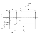
- FIG. 3 is a schematic view showing the optical fiber fixing structure 10, FIG. 3 (a) is a front view, and FIG. 3 (b) is an enlarged view of part A of FIG. 3 (a).
- the fiber fixing base 9 is provided with a groove 15 along the axial direction of the optical fiber 13 to be fixed.
- the groove 15 opens upward.
- the optical fiber 13 is disposed inside the groove 15 along the groove 15.
- the optical fiber 13 is fixed to the inner surface of the groove 15 with an adhesive 11.
- the inner surfaces of the grooves 15 facing each other serve as the fixing surface 17 of the optical fiber 13. That is, the optical fiber 13 is fixed by the adhesive 11 to the opposing fixed surface 17 that is the inner surface of the groove 15.
- a space 19 in which the adhesive 11 and the fiber fixing base 9 are not bonded is formed in the vertical direction of the optical fiber 13. That is, the space portion 19 is provided in the vertical direction substantially perpendicular to the fixing direction in which the optical fiber 13 is fixed.
- the width of the groove 15 (the distance between the fixing surfaces 17 in the fixing direction of the optical fiber 13 in the horizontal direction in FIG. 3B) is, for example, about 200 ⁇ m to 500 ⁇ m. If the width of the groove 15 is too large, the adhesive 11 tends to flow downward and may fill the space below. Further, if the width of the groove 15 is too narrow, the alignment width of the optical fiber 13 becomes narrow.
- the adhesive 11 is given a contraction force when it is cured.
- a force is a force from the surface of the adhesive 11 toward the fixing surface 17 (in the direction of arrow B in the figure).
- the optical fiber 13 is pulled in the direction of both the fixed surfaces 17. Accordingly, the force in the direction of the fixing surface 17 (left and right direction) is substantially canceled, and the positional deviation of the optical fiber 13 in the left and right direction when the adhesive 11 is cured and contracted can be suppressed.
- the vertical direction of the optical fiber 13 substantially the same force is applied in the vertical direction, and the optical fiber 13 is not pulled in one direction.
- the optical fiber 13 is fixed only to the opposing fixing surface 17 and the space portion 19 is provided in the direction perpendicular thereto, so that the optical fiber 13 and the fiber fixing base are disposed in the direction of the space portion 19. 9 is not joined. For this reason, when the adhesive agent 11 contracts, the stresses generated in the vertical direction and the horizontal direction are symmetrical, and the positional deviation of the optical fiber 13 can be suppressed.
- the depth of the groove 15 is sufficiently deep with respect to the width of the groove 15 (for example, the depth is 1.5 times or more of the width). This is because if the depth of the groove 15 is too shallow, the adhesive 11 flows and adheres to the bottom surface of the groove 15, making it difficult to form the space 19 appropriately.
- the viscosity of the adhesive 11 is preferably 10 to 200 Pa / s, for example, and more preferably 15 to 100 Pa / s. If the viscosity of the adhesive 11 is too low, the adhesive 11 tends to flow downward. Moreover, if the viscosity of the adhesive 11 is too high, alignment of the optical fiber 13 becomes difficult.
- Such adjustment of the viscosity can be adjusted by, for example, the filler content. When a large amount of filler is contained, the viscosity can be increased. Moreover, the shrinkage
- the width of the groove 15 differs depending on the position. Specifically, the lower groove width D is larger than the width C (interval between the fixing surfaces 17) of the fixing portion where the optical fiber 13 and the fiber fixing base 9 are fixed by the adhesive 11. That is, a step is formed in the lower portion of the fixed surface 17 by the interval changing portion 21a.
- the adhesive agent 11 flows below because the lower part of the fixed surface 17 to which the adhesive agent 11 was apply
- the optical fiber fixing structure 10b shown in FIG. the groove width below the optical fiber 13 and the fiber fixing base 9 is smaller than the width of the fixing portion (interval between the fixing surfaces 17) to which the optical fiber 13 and the fiber fixing base 9 are fixed. That is, a step is formed in the lower portion of the fixed surface 17 by the interval changing portion 21b. In this way, the adhesive 11 can be prevented from flowing downward from the fixed surface 17 by changing the interval regardless of the direction in which the step is formed.
- step difference is 0.1 mm or more, for example.
- the same effect can be obtained with the optical fiber fixing structure 10c shown in FIG.
- the lower portion of the fixing surface 17 is formed in a circular shape. Even in this case, the width of the groove changes in the lower portion of the fixed surface 17 by the interval changing portion 21c. As described above, if the changing portion of the width of the groove 15 is formed in the lower portion of the fixed surface 17, it is possible to prevent the adhesive 11 from flowing downward from the fixed surface 17 regardless of the form.
- the adhesive surface portion of the adhesive of the fixing surface 17 or the entire surface of the fixing surface 17 is processed into a ground glass shape to increase the surface roughness of the fixing surface 17, thereby increasing the surface tension effect of the adhesive. It is possible to prevent the adhesive from flowing downward.
- the surface roughness of the fixed surface 17 is preferably 0.8 ⁇ m to 25.0 ⁇ m, more preferably 1.0 ⁇ m to 12.5 ⁇ m, in terms of centerline average roughness (Ra).
- the optical fiber 13 is fixed to the pair of opposing fixing surfaces 17, the force in the direction of each fixing surface 17 is canceled when the adhesive 11 is cured and contracted.
- the positional deviation of the fiber 13 in the left-right direction can be suppressed.
- the optical fiber 13 is fixed to the fiber fixing base 9 symmetrically in the left-right direction (vertical symmetry) in the front view, even when the optical fiber 13 is pulled from the rear, It is possible to suppress the occurrence of a shift in the rotation direction.
- a space 19 is provided in the vertical direction of the optical fiber 13, and the tensile force accompanying the contraction of the adhesive 11 is symmetrical in the vertical direction. Therefore, the positional deviation of the optical fiber 13 in the vertical direction can also be suppressed.
- the surface of the adhesive 11 in the space 19 compensates for the shrinkage of the adhesive 11, an excessive tensile force is not applied to the surface of the optical fiber 13 or the vicinity of the fixing surface 17 of the pedestal. For this reason, the generation
- the depth sufficiently deep with respect to the width of the groove 15, it is possible to prevent the adhesive 11 from flowing downward, reaching the bottom surface of the groove 15, and filling the space 19. Moreover, if the viscosity of the adhesive agent 11 is set to an appropriate range, the space portion 19 can be secured more reliably. Furthermore, by forming the interval changing portion below the fixing portion of the groove 15 by the adhesive 11, it is possible to ensure the outflow of the adhesive 11 downward.
- FIG. 5 is a diagram showing a semiconductor laser module 1a according to the second embodiment.
- components having the same functions as those of the semiconductor laser module 1 are denoted by the same reference numerals as those in FIG.
- the semiconductor laser module 1a has substantially the same configuration as the semiconductor laser module 1, but the groove 15 is formed in a different direction.
- the groove 15 opens to the side. That is, the fixing surface 17 by the adhesive 11 is opposed in the vertical direction.
- the space portion 19 is formed in the opening direction of the groove 15 and in the left-right direction opposite to the opening direction. Even in this case, the space is formed in both directions perpendicular to the fixing direction (up and down direction in the figure) of the optical fiber 13 and the fiber fixing base 9 by the adhesive 11. Therefore, the same effect as that of the semiconductor laser module 1 can be obtained.
- FIG. 6 is a diagram illustrating a semiconductor laser module 1b according to the third embodiment.
- the semiconductor laser module 1b has substantially the same configuration as the semiconductor laser module 1, but the structure of the groove 15 is different.
- a split portion 23 is provided in the groove 15 of the semiconductor laser module 1 b, and a plurality of grooves 15 are provided in the axial direction of the optical fiber 13.
- FIG. 7 is a diagram showing an optical fiber fixing structure 10d in the semiconductor laser module 1b.
- a groove 15 is formed in the axial direction of the optical fiber 13 in the fiber fixing base 9a of the optical fiber fixing structure 10d. Further, the fiber fixing base 9 a is provided with a dividing portion 23 so as to be orthogonal to the groove 15 and to divide the groove 15. Therefore, the groove 15 is divided into a groove 15a and a groove 15b.
- the length E (the length in the axial direction of the optical fiber 13) of the groove 15a on the distal end side (semiconductor laser side) of the optical fiber 13 is shorter than the length F of the groove 15b far from the distal end side of the optical fiber 13. .
- the optical fiber 13 is fixed to the fiber fixing base 9a by the adhesive 11 on the fixing surfaces 17 facing each other, and the space portions 19 are formed in the vertical direction perpendicular to the optical fiber 13, respectively.
- Such an optical fiber fixing structure 10d is manufactured as follows. First, as shown in FIG. 6, the semiconductor laser base 5 and the fiber fixing base 9 a are fixed on the base 3, and further, the semiconductor laser 7 is fixed on the semiconductor laser base 5. Next, the optical fiber 13 is disposed in the groove 15 (grooves 15a and 15b) of the fiber fixing base 9a. At this time, an adhesive is applied only to the groove 15a.
- the adhesive 11 in the groove 15a is cured by heat, ultraviolet light or the like. After the adhesive 11 in the groove 15a is cured and the optical fiber 13 is fixed to the groove 15a, the adhesive 11 is applied to the groove 15b. In this state, since the alignment of the optical fiber 13 has already been completed, the adhesive 11 in the groove 15b is cured as it is.
- the reason why the optical fiber 13 is fixed to the fiber fixing base 9 in two stages of the grooves 15a and 15b is as follows. There is a possibility that force will be applied to the optical fiber 13 afterwards, such as a tension from the rear, while being fixed to the fiber fixing base 9. For this reason, a fixed strength (bonding strength) of a certain level or more is required. For this reason, the joining area of the optical fiber 13 and the fiber fixing base 9a (groove 15) is required. However, when the bonding area is increased, the amount of the adhesive 11 used is increased. For this reason, the alignment work of the optical fiber 13 becomes difficult, and the influence of the shrinkage of the adhesive 11 also increases.
- the optical fiber 13 is fixed to the groove 15a at a position close to the tip of the optical fiber 13. Since the length of the groove 15a is short, the amount of the adhesive 11 to be used can be reduced, and the alignment work becomes easy. Moreover, since the usage-amount of the adhesive agent 11 is small and joining length is short, the influence of the shrinkage
- the optical fiber 13 is fixed to the groove 15b having a longer length than the groove 15a.
- the length E of the groove 15a is preferably 1 ⁇ 2 or less, more preferably 1 / of the length F of the groove 15b.
- the same effect as the optical fiber fixing structure 10 can be obtained. Moreover, alignment workability
- operativity of the optical fiber 13 can be improved and the position shift of the optical fiber 13 can be suppressed more, ensuring the fixed strength of the optical fiber 13.
- FIG. 8A shows a semiconductor laser module 1c according to the fourth embodiment.
- the semiconductor laser module 1 c has substantially the same configuration as the semiconductor laser module 1, but differs in that a lens 25 is provided between the tip of the optical fiber 13 and the semiconductor laser 7.
- the lens 25 is, for example, a spherical lens.
- the lens 25 is held by a lens holder 27.
- the lens holder 27 is fixed on the base 3.
- the tip of the optical fiber 13 can be flat or obliquely polished. By doing so, the optical fiber 13 and the semiconductor laser 7 can be optically connected via the lens 25.
- a lens 25a and an isolator 29 may be provided between the optical fiber 13 and the semiconductor laser 7 as in the semiconductor laser module 1d shown in FIG.
- the lens 25a can be a spherical lens or an aspheric lens.
- the lens 25a is held by a lens holder 27a. Further, the lens holder 27 a and the isolator 29 are fixed on the base 3.
- the isolator 29 prevents incident light from being reflected back. By doing so, the optical fiber 13 and the semiconductor laser 7 can be optically connected via the lens 25 a and the isolator 29.
- FIG. 8 the example in which the lenses 25 and 25a are arranged with respect to the semiconductor laser module 1 is shown, but the present invention can also be applied to other semiconductor laser modules.
- the effect of the present invention was evaluated.
- the semiconductor laser module as shown in FIG. 1 the misalignment after the alignment was measured.
- the light intensity was detected with a photodetector connected to the optical fiber after the curing step of the adhesive after alignment, and the change was measured. The results are shown in FIG.
- FIG. 9 is a semiconductor laser module according to the present invention (structure of FIG. 1A), and a broken line L is a comparative example (structure of FIG. 10).
- borosilicate glass product name: Tempax
- the groove width of the base of the present invention was 0.25 mm.
- the dimension of the optical fiber used was set to ⁇ 0.125 mm. Although the results are omitted, the same results can be obtained with a special thin fiber having a diameter of 0.080 mm.
- An epoxy UV curable resin was used as the adhesive. The adhesive adhered to the optical fiber and placed in the groove, but the same result was obtained when the optical fiber was placed in the groove after a small amount of adhesive was placed from above the groove.
- the horizontal axis of the figure shows the manufacturing process, and the vertical axis shows the rate of change of light intensity.
- G in the figure is the light intensity after alignment, and this is used as a reference.
- H is a process in which the adhesive is irradiated with ultraviolet rays, and data was collected every 10 seconds.
- I represents a subsequent leaving step, and data was collected every 60 seconds. Note that the adhesive is cooled by the leaving step.
- J is when the chuck holding the optical fiber is released.
Abstract
This fixing structure for an optical fiber comprises a groove (15) that is provided to a fiber-fixing base (9) along the axial direction of an optical fiber (13) to be fixed. The groove (15) opens upward. The optical fiber (13) is arranged within the groove (15) along the groove (15). The optical fiber (13) is fixed to the inner surface of the groove (15) using an adhesive (11). On this occasion, the inner-side surfaces of the groove (15) that face each other serve as fixing surfaces (17) for the optical fiber (13). In other words, the optical fiber (13) is fixed to the fixing surfaces (17) that are the inner-side surfaces of the groove (15) and that face each other using the adhesive (11). A space (19) in which the fiber fixing base (9) and the adhesive are not bonded is formed in the vertical direction of the optical fiber (13). In other words, a space (19) is provided in a vertical direction that is substantially perpendicular to the fixing direction in which the optical fiber (13) is fixed.
Description
本発明は、光ファイバの位置ずれを防止可能であり、安定して光ファイバを固定可能な光ファイバの固定構造、半導体レーザモジュール、および光ファイバの固定方法に関するものである。
The present invention relates to an optical fiber fixing structure, a semiconductor laser module, and an optical fiber fixing method capable of preventing the optical fiber from being displaced and stably fixing the optical fiber.
従来用いられている半導体レーザモジュールにおいて、レーザダイオード(半導体レーザ)チップと光ファイバとは光学的に接続されている。この際、光ファイバは、半導体レーザとの光軸を合わせた後、台座上に半田や接着剤等によって固定される。
In a conventionally used semiconductor laser module, a laser diode (semiconductor laser) chip and an optical fiber are optically connected. At this time, the optical fiber is aligned on the optical axis with the semiconductor laser and then fixed on the pedestal with solder, an adhesive, or the like.
図10は、従来の半導体レーザモジュール100を示す概略図である。半導体レーザモジュール100は、ベース103上に、半導体レーザ台座105とファイバ固定台座109とが整列して配置される。半導体レーザ台座105上には、半導体レーザ107が固定される。また、ファイバ固定台座109には光ファイバ113が接着剤111等によって固定される。この状態で、光ファイバ113と半導体レーザ107とが光学的に結合される。なお、以下の説明において、光ファイバとファイバ固定台座との固定構造を、光ファイバ固定構造と称する。
FIG. 10 is a schematic view showing a conventional semiconductor laser module 100. In the semiconductor laser module 100, a semiconductor laser pedestal 105 and a fiber fixing pedestal 109 are arranged in alignment on a base 103. A semiconductor laser 107 is fixed on the semiconductor laser pedestal 105. An optical fiber 113 is fixed to the fiber fixing base 109 with an adhesive 111 or the like. In this state, the optical fiber 113 and the semiconductor laser 107 are optically coupled. In the following description, the fixing structure between the optical fiber and the fiber fixing base is referred to as an optical fiber fixing structure.
図11は、半導体レーザモジュール100における光ファイバ固定構造110を示す図で、図11(a)は側面図、図11(b)は正面図である。図11(a)に示すように、上面が平坦なファイバ固定台座109上には、上方に表面張力で盛り上がるように接着剤111が設けられ、接着剤111によって光ファイバ113が固定される。
FIG. 11 is a view showing the optical fiber fixing structure 110 in the semiconductor laser module 100, FIG. 11 (a) is a side view, and FIG. 11 (b) is a front view. As shown in FIG. 11A, an adhesive 111 is provided on the fiber fixing base 109 having a flat upper surface so as to rise upward due to surface tension, and the optical fiber 113 is fixed by the adhesive 111.
光ファイバ固定構造110では、光ファイバ113の下方のみにおいてファイバ固定台座109に固定される。すなわち、光ファイバ113の一方側のみがファイバ固定台座109に固定される。この場合、光ファイバ113の固定部の後方側で軸方向に力が付与されると(図中矢印G方向)、光ファイバ113の先端が上下にずれるように回転方向のずれが生じる(図中矢印H方向)。
The optical fiber fixing structure 110 is fixed to the fiber fixing base 109 only under the optical fiber 113. That is, only one side of the optical fiber 113 is fixed to the fiber fixing base 109. In this case, when a force is applied in the axial direction on the rear side of the fixed portion of the optical fiber 113 (in the direction of arrow G in the figure), the rotational direction shifts so that the tip of the optical fiber 113 is shifted up and down (in the figure). Arrow H direction).
また、図11(b)に示すように、このような光ファイバ固定構造110では、接着剤111が硬化する際の収縮によって、光ファイバ113には、ファイバ固定台座109方向に力が付与される(図中矢印I方向)。このように、ファイバ固定台座109に対する光ファイバ113の位置が、調心後、事後的に変動する恐れがある。
Further, as shown in FIG. 11B, in such an optical fiber fixing structure 110, a force is applied to the optical fiber 113 in the direction of the fiber fixing base 109 due to contraction when the adhesive 111 is cured. (Arrow I direction in the figure). As described above, the position of the optical fiber 113 with respect to the fiber fixing base 109 may change after the alignment.
このような光ファイバの位置ずれは、特にシングルモードのレンズドファイバの場合に大きな問題となる。すなわち、シングルモードのレンズドファイバのように、結合トレランスの特に狭い光学結合系を用いた半導体レーザモジュールにおいては、このような位置ずれが生じることで、半導体レーザと光ファイバとの光結合状態にずれが生じ、半導体レーザモジュールのファイバ端出力が劣化するという問題があった。
Such an optical fiber misalignment becomes a serious problem particularly in the case of a single mode lensed fiber. That is, in a semiconductor laser module using an optical coupling system with a particularly narrow coupling tolerance, such as a single mode lensed fiber, such a positional shift causes an optical coupling state between the semiconductor laser and the optical fiber. There was a problem that the fiber end output of the semiconductor laser module deteriorated due to the deviation.
特に、波長帯が980nm前後の半導体レーザとの光結合に用いられる光ファイバのように、先端形状が楔状の楔レンズドファイバを用いる場合には、その光結合の特性上、上下高さ方向の光結合トレランスが極端に狭いことから、ファイバ端出力の劣化は更に大きな問題となっていた。
In particular, when a wedged fiber having a wedge-shaped tip is used, such as an optical fiber used for optical coupling with a semiconductor laser having a wavelength band of about 980 nm, the vertical direction of the optical coupling characteristic is used. Since the optical coupling tolerance is extremely narrow, the degradation of the fiber end output has become an even greater problem.
これに対し、ファイバ固定台座に溝または孔を設け、光ファイバ113を溝または孔に配置した状態で、溝または孔に接着剤を充填し、光ファイバ113をファイバ固定台座に固定する方法がある(例えば、特許文献1、特許文献2)。
On the other hand, there is a method in which a groove or hole is provided in the fiber fixing base, and the optical fiber 113 is fixed to the fiber fixing base by filling the groove or hole with an adhesive in a state where the optical fiber 113 is disposed in the groove or hole. (For example, Patent Document 1 and Patent Document 2).
図12(a)は、略矩形断面の溝を有するファイバ固定台座109aを用いた光ファイバ固定構造110aを示す図である。光ファイバ固定構造110aは、ファイバ固定台座109aに形成された溝内に光ファイバ113が配置され、溝に充填された接着剤111によって光ファイバ113がファイバ固定台座109aに固定される。
FIG. 12A is a view showing an optical fiber fixing structure 110a using a fiber fixing base 109a having a groove having a substantially rectangular cross section. In the optical fiber fixing structure 110a, the optical fiber 113 is disposed in a groove formed in the fiber fixing base 109a, and the optical fiber 113 is fixed to the fiber fixing base 109a by an adhesive 111 filled in the groove.
しかし、光ファイバ固定構造110aは、矩形溝に対し、光ファイバ113が左右及び下方の3方向でファイバ固定台座109aに固定されるものであるが、このようにしても、接着剤111の硬化時の収縮によって、下方及び左右方向(図中矢印J方向)に光ファイバ113が応力を受ける。したがって、接着剤硬化時に光ファイバ113の先端位置がずれる恐れがある。
However, in the optical fiber fixing structure 110a, the optical fiber 113 is fixed to the fiber fixing base 109a in the three directions of right and left and lower with respect to the rectangular groove. Due to the contraction of the optical fiber 113, the optical fiber 113 is stressed downward and in the left-right direction (in the direction of arrow J in the figure). Therefore, the tip position of the optical fiber 113 may be shifted when the adhesive is cured.
また、図12(b)は、円形の孔を有するファイバ固定台座109bを用いた光ファイバ固定構造110bを示す図である。光ファイバ固定構造110bは、ファイバ固定台座109bに形成された孔内に光ファイバ113が挿通され、孔に充填された接着剤111によって光ファイバ113がファイバ固定台座109bに固定される。
FIG. 12B is a view showing an optical fiber fixing structure 110b using a fiber fixing base 109b having a circular hole. In the optical fiber fixing structure 110b, the optical fiber 113 is inserted into a hole formed in the fiber fixing base 109b, and the optical fiber 113 is fixed to the fiber fixing base 109b with an adhesive 111 filled in the hole.
光ファイバ固定構造110bでは、接着剤111の硬化収縮時に、孔内の光ファイバ113は、全方向に略均一な応力を受ける(図中矢印K方向)。しかし、接着剤111の硬化収縮時には、光ファイバ113の表面が全方向に引っ張られ、圧縮の応力が付与される。また、接着後の温度変化によって、接着剤の膨張や収縮が生じ、光ファイバ113の全周に圧縮や引っ張りの応力が付与される。このような場合、接着剤の全周が孔によって規制されているため、応力が解放できず、接着剤111がファイバ固定台座109bまたは光ファイバ113表面から剥離したり、ファイバ固定台座109bの表面に亀裂が生じる等の恐れがある。
In the optical fiber fixing structure 110b, when the adhesive 111 is cured and contracted, the optical fiber 113 in the hole receives substantially uniform stress in all directions (in the direction of arrow K in the figure). However, when the adhesive 111 is cured and contracted, the surface of the optical fiber 113 is pulled in all directions, and compressive stress is applied. Further, the temperature change after bonding causes expansion and contraction of the adhesive, and compressive or tensile stress is applied to the entire circumference of the optical fiber 113. In such a case, since the entire circumference of the adhesive is regulated by the holes, the stress cannot be released, and the adhesive 111 is peeled off from the surface of the fiber fixing base 109b or the optical fiber 113, or on the surface of the fiber fixing base 109b. There is a risk of cracking.
本発明は、このような問題に鑑みてなされたもので、光ファイバの位置ずれを防止し、安定して光ファイバを固定可能な光ファイバの固定構造等を提供することを目的とする。
The present invention has been made in view of such a problem, and an object of the present invention is to provide an optical fiber fixing structure or the like that can prevent the positional deviation of the optical fiber and can stably fix the optical fiber.
前述した目的を達成するために第1の発明は、光ファイバの固定構造であって、台座と前記台座に固定部材で固定される光ファイバと、を具備し、前記台座には、前記光ファイバの軸方向に沿って溝が形成され、前記光ファイバは、前記溝の内面の互いに対向する固定面に、前記固定部材で固定され、前記光ファイバの軸方向から見て、前記光ファイバと前記固定面との固定方向と略垂直な両方向には、前記光ファイバが前記台座に固定されない空間部が形成されることを特徴とする光ファイバの固定構造である。
In order to achieve the above-mentioned object, a first invention is an optical fiber fixing structure, comprising a pedestal and an optical fiber fixed to the pedestal with a fixing member, and the pedestal includes the optical fiber. A groove is formed along the axial direction of the optical fiber, and the optical fiber is fixed to the mutually facing fixed surfaces of the inner surface of the groove by the fixing member, and when viewed from the axial direction of the optical fiber, the optical fiber and the optical fiber A space structure in which the optical fiber is not fixed to the base is formed in both directions substantially perpendicular to the fixing direction with the fixing surface.
前記溝は、前記台座の上面に形成され、前記光ファイバは、前記溝の内側面である前記固定面に前記固定部材により固定され、前記溝の底部側には、前記光ファイバが固定された部位における前記固定面同士の間隔とは間隔が変化する、間隔変化部が形成させてもよい。
The groove is formed on an upper surface of the pedestal, the optical fiber is fixed to the fixing surface which is an inner surface of the groove by the fixing member, and the optical fiber is fixed to the bottom side of the groove. An interval changing portion in which the interval is different from the interval between the fixed surfaces in the part may be formed.
前記溝は、前記光ファイバの軸方向に複数設けられ、前記光ファイバの先端に近い側の前記溝の長さは、前記光ファイバの先端から遠い側の前記溝の長さよりも短くしてもよい。
A plurality of the grooves are provided in the axial direction of the optical fiber, and the length of the groove near the tip of the optical fiber may be shorter than the length of the groove far from the tip of the optical fiber. Good.
第1の発明によれば、台座に形成された溝の一方の対向面にのみ固定部材で光ファイバが固定される。また、光ファイバの固定方向と垂直な方向には、台座と光ファイバとが固定されない空間部が形成される。このため、接着剤の収縮による力が相殺されて、光ファイバの位置ずれが抑制される。また、空間部が形成されるため、接着剤の膨張や収縮時には、空間部が形状変化の逃げ部となる。したがって、光ファイバの外周に過剰な力が付与されることを抑制することができる。
According to the first aspect of the invention, the optical fiber is fixed by the fixing member only to one facing surface of the groove formed in the pedestal. In addition, a space portion in which the base and the optical fiber are not fixed is formed in a direction perpendicular to the fixing direction of the optical fiber. For this reason, the force by shrinkage | contraction of an adhesive agent is canceled, and the position shift of an optical fiber is suppressed. Further, since the space portion is formed, the space portion becomes an escape portion of the shape change when the adhesive is expanded or contracted. Therefore, it is possible to suppress an excessive force from being applied to the outer periphery of the optical fiber.
また、光ファイバを左右方向の固定面で固定支持した際に、下方に、溝内面の間隔が変化する間隔変化部を形成することで、硬化前の接着剤が下方に流れることを抑制することができる。したがって、接着剤が下方に流れ、図12(a)に示したように、溝が接着剤で埋まることを抑制することができる。
In addition, when the optical fiber is fixed and supported by the fixing surface in the left-right direction, an interval changing portion that changes the interval between the groove inner surfaces is formed below to suppress the adhesive from flowing downward before curing. Can do. Therefore, it is possible to prevent the adhesive from flowing downward and filling the groove with the adhesive as shown in FIG.
また、溝が光ファイバの軸方向に複数形成され、光ファイバの先端側の短い溝部と、他方の長い溝部に分けることで、光ファイバをより精度良く台座に固定することができる。例えば、短い溝に光ファイバを固定する場合には、接着剤の使用量も少量で済むため、接着剤による位置ずれの影響を抑えることができる。一方、少量の接着剤では、十分な固定強度を得ることができないため、長い側の溝で光ファイバを固定し、十分な固定強度を確保することができる。
Also, a plurality of grooves are formed in the axial direction of the optical fiber, and the optical fiber can be fixed to the pedestal with higher accuracy by dividing the optical fiber into a short groove on the tip side and the other long groove. For example, when an optical fiber is fixed in a short groove, the amount of adhesive used is small, so that it is possible to suppress the influence of misalignment due to the adhesive. On the other hand, since a sufficient amount of fixing strength cannot be obtained with a small amount of adhesive, it is possible to secure the sufficient fixing strength by fixing the optical fiber with the long groove.
第2の発明は、第1の発明にかかる光ファイバの固定構造を有し、ベースと、前記ベース上に設けられる前記光ファイバの固定構造と、前記光ファイバの固定構造における前記光ファイバと光接続される半導体レーザと、を具備することを特徴とする半導体レーザモジュールである。
A second invention has an optical fiber fixing structure according to the first invention, and includes a base, the optical fiber fixing structure provided on the base, and the optical fiber and light in the optical fiber fixing structure. And a semiconductor laser connected to the semiconductor laser module.
前記半導体レーザと前記光ファイバとの間には、レンズと、アイソレータと、が設けられてもよい。
A lens and an isolator may be provided between the semiconductor laser and the optical fiber.
第2の発明によれば、光ファイバと半導体レーザとの光結合状態のずれが小さく、ファイバ端出力の劣化の少ない半導体レーザモジュールを得ることができる。
According to the second invention, it is possible to obtain a semiconductor laser module in which the optical coupling state between the optical fiber and the semiconductor laser is small and the fiber end output is less deteriorated.
第3の発明は、光ファイバの固定方法であって、前記光ファイバを、溝を有する台座の前記溝に配置する工程と、前記光ファイバと前記溝の内面の互いに対向する固定面との間に、固定部材を塗布する工程と、前記固定部材を硬化させて、前記台座に前記光ファイバを固定する工程と、有し、前記光ファイバは、前記光ファイバの軸方向から見て、前記光ファイバと前記固定面との固定方向と略垂直な両方向には、前記光ファイバが前記台座に固定されない空間部が形成されるように固定されることを特徴とする光ファイバの固定方法である。
A third invention is an optical fiber fixing method, wherein the optical fiber is disposed in the groove of a pedestal having a groove, and the optical fiber and an inner surface of the groove are opposed to each other. And applying the fixing member; and curing the fixing member to fix the optical fiber to the pedestal. The optical fiber viewed from the axial direction of the optical fiber, In the optical fiber fixing method, the optical fiber is fixed so as to form a space portion in which the optical fiber is not fixed to the base in both directions substantially perpendicular to the fixing direction of the fiber and the fixing surface.
前記光ファイバの先端に近い側の第1溝の長さは、前記光ファイバの先端から遠い側の第2溝の長さよりも短く、前記光ファイバと前記第1溝の前記固定面との間に前記固定部材を塗布する工程と、前記第1溝の前記固定部材を硬化させて、前記台座に前記光ファイバを固定する工程と、前記光ファイバと前記第2溝の前記固定面との間に前記固定部材を塗布する工程と、前記第2溝の前記固定部材を硬化させて、前記台座に前記光ファイバを固定する工程と、を有し、前記光ファイバは、前記第1溝および前記第2溝において、前記光ファイバの軸方向から見て、前記光ファイバと前記固定面との固定方向と略垂直な両方向には、前記光ファイバが前記台座に固定されない空間部が形成されるように固定されてもよい。
The length of the first groove near the tip of the optical fiber is shorter than the length of the second groove far from the tip of the optical fiber, and is between the optical fiber and the fixed surface of the first groove. Applying the fixing member to the base, curing the fixing member in the first groove to fix the optical fiber to the base, and between the optical fiber and the fixing surface of the second groove. Applying the fixing member to the base, and curing the fixing member in the second groove to fix the optical fiber to the pedestal, wherein the optical fiber includes the first groove and the In the second groove, a space where the optical fiber is not fixed to the pedestal is formed in both directions substantially perpendicular to the fixing direction of the optical fiber and the fixing surface when viewed from the axial direction of the optical fiber. It may be fixed to.
第3の発明によれば、光ファイバと半導体レーザとの光結合状態のずれが小さく、ファイバ端出力の劣化の少ない半導体レーザモジュールを容易に得ることができる。
According to the third invention, it is possible to easily obtain a semiconductor laser module in which the optical coupling state between the optical fiber and the semiconductor laser is small and the fiber end output is less deteriorated.
また、光ファイバの軸方向に複数形成された溝に対し、まず、短い溝に光ファイバを固定するため、光ファイバの先端に近い位置を少量の接着剤で固定することが可能であるため、接着剤による位置ずれの影響を抑えることができる。また、短い溝への固定完了後に、長い側の溝で光ファイバを固定するため、十分な固定強度を確保することができる。
In addition, for the plurality of grooves formed in the axial direction of the optical fiber, first, the optical fiber is fixed in a short groove, so it is possible to fix the position close to the tip of the optical fiber with a small amount of adhesive, It is possible to suppress the influence of positional deviation due to the adhesive. Further, since the optical fiber is fixed by the long groove after the fixing to the short groove is completed, sufficient fixing strength can be ensured.
本発明によれば、光ファイバの位置ずれを防止し、安定して光ファイバを固定可能な光ファイバの固定構造等を提供することができる。
According to the present invention, it is possible to provide an optical fiber fixing structure or the like that can prevent the positional deviation of the optical fiber and can stably fix the optical fiber.
以下、図面を参照しながら、本発明の実施形態について説明する。図1(a)は、半導体レーザモジュール1の斜視図である。半導体レーザモジュール1は、主に、ベース3、半導体レーザ台座5、半導体レーザ7、ファイバ固定台座9、光ファイバ13等から構成される。
Hereinafter, embodiments of the present invention will be described with reference to the drawings. FIG. 1A is a perspective view of the semiconductor laser module 1. The semiconductor laser module 1 mainly includes a base 3, a semiconductor laser base 5, a semiconductor laser 7, a fiber fixing base 9, an optical fiber 13, and the like.
ベース3は、上部に各構成が設置される板状の部材である。ベース3としては、例えば、AlN、CuW、Al2O3等を用いることができ、熱伝導性に優れる材質であることが望ましい。
The base 3 is a plate-like member in which each component is installed in the upper part. As the base 3, for example, AlN, CuW, Al 2 O 3 or the like can be used, and it is desirable that the base 3 be made of a material having excellent thermal conductivity.
ベース3上には、半田等によって半導体レーザ台座5が固定される。半導体レーザ台座5は上部に半導体レーザ7が固定される部材である。半導体レーザ台座5としては、例えば、AlN、CuW、Cu、Si等を用いることができ、また、半導体レーザ7は、所望の波長のレーザを発光することが可能である、例えばInPレーザ、GaAsレーザ、GaAsAlレーザ等を用いることができる。
The semiconductor laser pedestal 5 is fixed on the base 3 with solder or the like. The semiconductor laser pedestal 5 is a member to which the semiconductor laser 7 is fixed. As the semiconductor laser pedestal 5, for example, AlN, CuW, Cu, Si or the like can be used, and the semiconductor laser 7 can emit a laser having a desired wavelength, for example, an InP laser or a GaAs laser. A GaAsAl laser or the like can be used.
ベース3上には半導体レーザ台座5と併設するように、ファイバ固定台座9が半田や接着剤等によって固定される。ファイバ固定台座9としては、例えば、ホウケイ酸ガラスや石英ガラス等のガラス材や、AlN、CuW、Al2O3等を用いることができる。なお、図1(b)に示すように、ファイバ固定台座9は、ベース3に対して一体で構成することもできる。また、図2に示すように、半導体レーザ台座5とファイバ固定台座9とを一体で構成してもよい。この場合、一体化された台座が半田等によってベース3に固定される。ここで、図2に示すように、半導体レーザ台座5とファイバ固定台座9とを一体で構成する場合には、ベース3は必ずしも必要ではない。なお、以下の説明においては、ファイバ固定台座9がベース3とは別体で構成され、ベース3上に接合された例について説明する。
A fiber fixing base 9 is fixed on the base 3 with solder, an adhesive, or the like so as to be provided with the semiconductor laser base 5. As the fiber fixing base 9, for example, a glass material such as borosilicate glass or quartz glass, AlN, CuW, Al 2 O 3 or the like can be used. As shown in FIG. 1B, the fiber fixing base 9 can be configured integrally with the base 3. Further, as shown in FIG. 2, the semiconductor laser base 5 and the fiber fixing base 9 may be integrally formed. In this case, the integrated pedestal is fixed to the base 3 with solder or the like. Here, as shown in FIG. 2, when the semiconductor laser base 5 and the fiber fixing base 9 are integrally formed, the base 3 is not necessarily required. In the following description, an example will be described in which the fiber fixing base 9 is formed separately from the base 3 and is bonded onto the base 3.
ファイバ固定台座9の上面には、光ファイバ13が接着剤11によって固定される。接着剤11としては、例えば、UV硬化系、熱硬化系、UV硬化+熱硬化系、常温放置硬化系などを用いることができる。この状態で、光ファイバ13と半導体レーザ7とが光学的に結合される。なお、光ファイバ13を固定するための固定部材としては、接着剤11ではなく、半田を用いても良い。この場合、半田材として、例えばAuSn、SnAgCu、SnBi等を用いることができる。なお、以下の説明では、固定部材として接着剤11を用い、接着剤11が硬化収縮する例について説明するが、半田を用いた場合において、半田の凝固収縮に対しても同様の効果を得ることができる。
An optical fiber 13 is fixed to the upper surface of the fiber fixing base 9 with an adhesive 11. As the adhesive 11, for example, a UV curing system, a thermosetting system, a UV curing + thermosetting system, a room temperature standing curing system, or the like can be used. In this state, the optical fiber 13 and the semiconductor laser 7 are optically coupled. In addition, as a fixing member for fixing the optical fiber 13, not the adhesive 11 but solder may be used. In this case, for example, AuSn, SnAgCu, SnBi or the like can be used as a solder material. In the following description, an example in which the adhesive 11 is used as the fixing member and the adhesive 11 cures and shrinks will be described. However, in the case where solder is used, the same effect can be obtained for the solidification shrinkage of the solder. Can do.
光ファイバ13と半導体レーザ7との調芯は、例えば、光ファイバ13に半導体レーザ7から光を入射させた状態で、光ファイバ13を半導体レーザ7に対して相対移動させて行われる。光ファイバ13は、光ファイバ13をチャックしているハンド(図示せず)によって移動させる。光ファイバ13に接続された光検出器で検出される光強度が最大となるように位置決めを行い、所定以上の強度が検出された状態で位置決め作業を終了する。この状態で、接着剤11に熱や紫外線を照射する等により、接着剤11を硬化させる。以上により、光ファイバ13が適切な位置でファイバ固定台座9上に固定される。
Alignment between the optical fiber 13 and the semiconductor laser 7 is performed, for example, by moving the optical fiber 13 relative to the semiconductor laser 7 in a state where light is incident on the optical fiber 13 from the semiconductor laser 7. The optical fiber 13 is moved by a hand (not shown) that chucks the optical fiber 13. Positioning is performed so that the light intensity detected by the light detector connected to the optical fiber 13 is maximized, and the positioning operation is completed in a state where a predetermined intensity or more is detected. In this state, the adhesive 11 is cured by irradiating the adhesive 11 with heat or ultraviolet rays. Thus, the optical fiber 13 is fixed on the fiber fixing base 9 at an appropriate position.
図3は、光ファイバ固定構造10を示す概略図であり、図3(a)は正面図、図3(b)は図3(a)のA部拡大図である。ファイバ固定台座9には、固定される光ファイバ13の軸方向に沿って溝15が設けられる。溝15は、上方に開口する。光ファイバ13は、溝15に沿って、溝15の内部に配置される。
FIG. 3 is a schematic view showing the optical fiber fixing structure 10, FIG. 3 (a) is a front view, and FIG. 3 (b) is an enlarged view of part A of FIG. 3 (a). The fiber fixing base 9 is provided with a groove 15 along the axial direction of the optical fiber 13 to be fixed. The groove 15 opens upward. The optical fiber 13 is disposed inside the groove 15 along the groove 15.
光ファイバ13は、溝15の内面に対して接着剤11によって固定されている。この際、溝15の互いに対向する内側面が、光ファイバ13の固定面17となる。すなわち、光ファイバ13は、溝15の内側面である対向する固定面17に対して接着剤11によって固定される。
The optical fiber 13 is fixed to the inner surface of the groove 15 with an adhesive 11. At this time, the inner surfaces of the grooves 15 facing each other serve as the fixing surface 17 of the optical fiber 13. That is, the optical fiber 13 is fixed by the adhesive 11 to the opposing fixed surface 17 that is the inner surface of the groove 15.
この際、図3(b)に示すように、光ファイバ13の上下方向には、接着剤11とファイバ固定台座9とが接着されない空間部19が形成される。すなわち、光ファイバ13が固定される固定方向に対して、略垂直な上下方向に、空間部19が設けられる。
At this time, as shown in FIG. 3 (b), a space 19 in which the adhesive 11 and the fiber fixing base 9 are not bonded is formed in the vertical direction of the optical fiber 13. That is, the space portion 19 is provided in the vertical direction substantially perpendicular to the fixing direction in which the optical fiber 13 is fixed.
なお、光ファイバ13としては、例えば125μmのレンズドファイバを用いることができる。この際、溝15の幅(図3(b)の左右方向であって、光ファイバ13の固定方向の固定面17同士の間隔)は、例えば200μm~500μm程度とする。溝15の幅が大きすぎると、接着剤11が下部に流れやすくなり、下方の空間を埋めてしまう恐れがある。また、溝15の幅が狭すぎると、光ファイバ13の調心幅が狭くなるためである。
For example, a 125 μm lensed fiber can be used as the optical fiber 13. At this time, the width of the groove 15 (the distance between the fixing surfaces 17 in the fixing direction of the optical fiber 13 in the horizontal direction in FIG. 3B) is, for example, about 200 μm to 500 μm. If the width of the groove 15 is too large, the adhesive 11 tends to flow downward and may fill the space below. Further, if the width of the groove 15 is too narrow, the alignment width of the optical fiber 13 becomes narrow.
図3(b)に示すように、接着剤11には、硬化する際の収縮力が付与される。このような力は、接着剤11の表面から、固定面17方向への力となる(図中矢印B方向)。本実施形態では、光ファイバ13は、両方の固定面17方向へ引っ張られる。したがって、固定面17方向(左右方向)の力は略相殺されて、接着剤11の硬化収縮時における、光ファイバ13の左右方向への位置ずれを抑制することができる。一方、光ファイバ13の上下方向に対しては、上下方向に略同様の力が付与され、一方の方向へ光ファイバ13が引っ張られることがない。したがって、接着剤11の硬化収縮時における、光ファイバ13の上下方向の位置ずれを抑制することができる。この際、光ファイバ13の上下方向の接着剤11は、左右方向(固定面17方向)への接着剤11の収縮に補填される。したがって、光ファイバ13の表面に対して、過剰な引張力が付与されることがない。
As shown in FIG. 3 (b), the adhesive 11 is given a contraction force when it is cured. Such a force is a force from the surface of the adhesive 11 toward the fixing surface 17 (in the direction of arrow B in the figure). In the present embodiment, the optical fiber 13 is pulled in the direction of both the fixed surfaces 17. Accordingly, the force in the direction of the fixing surface 17 (left and right direction) is substantially canceled, and the positional deviation of the optical fiber 13 in the left and right direction when the adhesive 11 is cured and contracted can be suppressed. On the other hand, in the vertical direction of the optical fiber 13, substantially the same force is applied in the vertical direction, and the optical fiber 13 is not pulled in one direction. Therefore, it is possible to suppress the vertical displacement of the optical fiber 13 when the adhesive 11 is cured and contracted. At this time, the adhesive 11 in the vertical direction of the optical fiber 13 is compensated for contraction of the adhesive 11 in the left-right direction (direction of the fixed surface 17). Therefore, an excessive tensile force is not applied to the surface of the optical fiber 13.
このように、対向する固定面17に対してのみ光ファイバ13を固定し、これと垂直な方向に対しては空間部19を設けるため、空間部19の方向には光ファイバ13とファイバ固定台座9とが接合されることがない。このため、接着剤11が収縮する際に、上下方向、左右方向に生じる応力がそれぞれ対称になり、光ファイバ13の位置ずれを抑制することができる。
In this way, the optical fiber 13 is fixed only to the opposing fixing surface 17 and the space portion 19 is provided in the direction perpendicular thereto, so that the optical fiber 13 and the fiber fixing base are disposed in the direction of the space portion 19. 9 is not joined. For this reason, when the adhesive agent 11 contracts, the stresses generated in the vertical direction and the horizontal direction are symmetrical, and the positional deviation of the optical fiber 13 can be suppressed.
なお、溝15の深さは、溝15の幅に対して十分に深くする(例えば、深さを幅の1.5倍以上とする)。溝15の深さが浅すぎると、接着剤11が流れて溝15の底面に付着し、空間部19を適切に形成することが困難となるためである。また、接着剤11の粘度は、例えば10~200Pa/sとすることが望ましく、さらに望ましくは、15~100Pa/sである。接着剤11の粘度が低すぎると、接着剤11が下方に流れやすくなる。また、接着剤11の粘度が高すぎると、光ファイバ13の調心が困難となる。このような粘度の調整は、例えばフィラーの含有量によっても調整することができる。フィラーを多く含有させると、粘度を上げることができる。また、フィラーを含有させることで、接着剤11の硬化時の収縮量を小さくすることもできる。
Note that the depth of the groove 15 is sufficiently deep with respect to the width of the groove 15 (for example, the depth is 1.5 times or more of the width). This is because if the depth of the groove 15 is too shallow, the adhesive 11 flows and adheres to the bottom surface of the groove 15, making it difficult to form the space 19 appropriately. The viscosity of the adhesive 11 is preferably 10 to 200 Pa / s, for example, and more preferably 15 to 100 Pa / s. If the viscosity of the adhesive 11 is too low, the adhesive 11 tends to flow downward. Moreover, if the viscosity of the adhesive 11 is too high, alignment of the optical fiber 13 becomes difficult. Such adjustment of the viscosity can be adjusted by, for example, the filler content. When a large amount of filler is contained, the viscosity can be increased. Moreover, the shrinkage | contraction amount at the time of hardening of the adhesive agent 11 can also be made small by containing a filler.
また、図4(a)に示すように、接着剤11が下方へ流れることを構造的に抑制することもできる。光ファイバ固定構造10aは、溝15の幅が、位置によって異なる。具体的には、光ファイバ13とファイバ固定台座9とが接着剤11によって固定される固定部の幅C(固定面17同士の間隔)に対して、その下方の溝幅Dが大きい。すなわち、固定面17の下部には、間隔変化部21aによって、段差が形成される。このように接着剤11が塗布された固定面17の下部が直線ではなく、段差となることで、接着剤11が下方に流れることを抑制することができる。
Moreover, as shown to Fig.4 (a), it can also suppress structurally that the adhesive agent 11 flows downward. In the optical fiber fixing structure 10a, the width of the groove 15 differs depending on the position. Specifically, the lower groove width D is larger than the width C (interval between the fixing surfaces 17) of the fixing portion where the optical fiber 13 and the fiber fixing base 9 are fixed by the adhesive 11. That is, a step is formed in the lower portion of the fixed surface 17 by the interval changing portion 21a. Thus, it can suppress that the adhesive agent 11 flows below because the lower part of the fixed surface 17 to which the adhesive agent 11 was apply | coated becomes a level | step difference instead of a straight line.
このような効果は、図4(b)に示す光ファイバ固定構造10bでも得ることができる。光ファイバ固定構造10bは、光ファイバ13とファイバ固定台座9とが接着剤11によって固定される固定部の幅(固定面17同士の間隔)に対して、その下方の溝幅が小さい。すなわち、固定面17の下部には、間隔変化部21bによって、段差が形成される。このように、段差の形成方向によらず、間隔を変化させることで、固定面17から接着剤11が下方に流れることを抑制することができる。なお、段差はたとえば0.1mm以上であることが好ましい。
Such an effect can also be obtained by the optical fiber fixing structure 10b shown in FIG. In the optical fiber fixing structure 10b, the groove width below the optical fiber 13 and the fiber fixing base 9 is smaller than the width of the fixing portion (interval between the fixing surfaces 17) to which the optical fiber 13 and the fiber fixing base 9 are fixed. That is, a step is formed in the lower portion of the fixed surface 17 by the interval changing portion 21b. In this way, the adhesive 11 can be prevented from flowing downward from the fixed surface 17 by changing the interval regardless of the direction in which the step is formed. In addition, it is preferable that a level | step difference is 0.1 mm or more, for example.
また、図4(c)に示す光ファイバ固定構造10cでも同様の効果を得ることができる。光ファイバ固定構造10cは、固定面17の下部が、円形に形成される。この場合でも、固定面17の下部には、間隔変化部21cによって、溝の幅が変化する。このように、固定面17の下部に、溝15の幅の変化部が形成されれば、その形態によらず、固定面17から接着剤11が下方に流れることを抑制することができる。
Also, the same effect can be obtained with the optical fiber fixing structure 10c shown in FIG. In the optical fiber fixing structure 10c, the lower portion of the fixing surface 17 is formed in a circular shape. Even in this case, the width of the groove changes in the lower portion of the fixed surface 17 by the interval changing portion 21c. As described above, if the changing portion of the width of the groove 15 is formed in the lower portion of the fixed surface 17, it is possible to prevent the adhesive 11 from flowing downward from the fixed surface 17 regardless of the form.
また、固定面17の接着剤の接着面部分又は固定面17全面に対して、すりガラス状に粗く加工して、固定面17の表面粗さを粗くすることで、接着剤の表面張力効果を高めることができ、接着剤が下方に流れることを抑制することができる。このとき、固定面17の表面粗さは中心線平均粗さ(Ra)で0.8μm~25.0μmが好ましく、1.0μm~12.5μmであることがさらに好ましい。
Further, the adhesive surface portion of the adhesive of the fixing surface 17 or the entire surface of the fixing surface 17 is processed into a ground glass shape to increase the surface roughness of the fixing surface 17, thereby increasing the surface tension effect of the adhesive. It is possible to prevent the adhesive from flowing downward. At this time, the surface roughness of the fixed surface 17 is preferably 0.8 μm to 25.0 μm, more preferably 1.0 μm to 12.5 μm, in terms of centerline average roughness (Ra).
以上、本実施の形態によれば、光ファイバ13が対向する一対の固定面17に固定されるため、接着剤11の硬化収縮時に、それぞれの固定面17の方向への力が相殺され、光ファイバ13の左右方向への位置ずれを抑制することができる。また、光ファイバ13は、正面視において、左右対称(上下対称)にファイバ固定台座9に固定されるため、光ファイバ13が後方から引っ張られた際にも、光ファイバ13の先端に、上下左右の回転方向のずれが生じることを抑制することができる。
As described above, according to the present embodiment, since the optical fiber 13 is fixed to the pair of opposing fixing surfaces 17, the force in the direction of each fixing surface 17 is canceled when the adhesive 11 is cured and contracted. The positional deviation of the fiber 13 in the left-right direction can be suppressed. Further, since the optical fiber 13 is fixed to the fiber fixing base 9 symmetrically in the left-right direction (vertical symmetry) in the front view, even when the optical fiber 13 is pulled from the rear, It is possible to suppress the occurrence of a shift in the rotation direction.
また、光ファイバ13の上下方向には、空間部19が設けられ、接着剤11の収縮に伴う引張力は上下方向に対称となる。したがって、光ファイバ13の上下方向の位置ずれも抑制することができる。この際、空間部19における接着剤11の表面は、接着剤11の収縮を補填するため、光ファイバ13表面や台座の固定面17付近に対して過剰な引張力が付与されることがない。このため、光ファイバ13表面や台座の固定面17付近の亀裂の発生などを防止することができる。
Further, a space 19 is provided in the vertical direction of the optical fiber 13, and the tensile force accompanying the contraction of the adhesive 11 is symmetrical in the vertical direction. Therefore, the positional deviation of the optical fiber 13 in the vertical direction can also be suppressed. At this time, since the surface of the adhesive 11 in the space 19 compensates for the shrinkage of the adhesive 11, an excessive tensile force is not applied to the surface of the optical fiber 13 or the vicinity of the fixing surface 17 of the pedestal. For this reason, the generation | occurrence | production of the crack of the optical fiber 13 surface or the fixing surface 17 vicinity of a base can be prevented.
特に、溝15の幅に対して深さを十分に深くすることで、接着剤11が下方に流れて、溝15の底面に達し、空間部19が埋まることを防止することができる。また、接着剤11の粘度を適正範囲とすれば、より確実に空間部19を確保することができる。さらに、溝15の接着剤11による固定部の下方に間隔変化部を形成することで、接着剤11の下方への流出を確実に確保することができる。
In particular, by making the depth sufficiently deep with respect to the width of the groove 15, it is possible to prevent the adhesive 11 from flowing downward, reaching the bottom surface of the groove 15, and filling the space 19. Moreover, if the viscosity of the adhesive agent 11 is set to an appropriate range, the space portion 19 can be secured more reliably. Furthermore, by forming the interval changing portion below the fixing portion of the groove 15 by the adhesive 11, it is possible to ensure the outflow of the adhesive 11 downward.
次に、他の実施の形態について説明する。図5は、第2の実施の形態にかかる半導体レーザモジュール1aを示す図である。なお、以下の説明において、半導体レーザモジュール1と同様の機能を奏する構成については、図1等と同一の符号を付し、重複する説明を省略する。
Next, another embodiment will be described. FIG. 5 is a diagram showing a semiconductor laser module 1a according to the second embodiment. In the following description, components having the same functions as those of the semiconductor laser module 1 are denoted by the same reference numerals as those in FIG.
半導体レーザモジュール1aは、半導体レーザモジュール1と略同様の構成であるが、溝15の形成方向が異なる。半導体レーザモジュール1aでは、溝15が側方に向けて開口する。すなわち、接着剤11による固定面17は、上下方向に対向する。この場合には、溝15の開口方向および開口方向とは逆方向の左右方向に空間部19が形成される。この場合であっても、接着剤11による光ファイバ13とファイバ固定台座9との固定方向(図中上下方向)に対して、垂直な両方向に空間部が形成される。したがって、半導体レーザモジュール1と同様の効果を得ることができる。
The semiconductor laser module 1a has substantially the same configuration as the semiconductor laser module 1, but the groove 15 is formed in a different direction. In the semiconductor laser module 1a, the groove 15 opens to the side. That is, the fixing surface 17 by the adhesive 11 is opposed in the vertical direction. In this case, the space portion 19 is formed in the opening direction of the groove 15 and in the left-right direction opposite to the opening direction. Even in this case, the space is formed in both directions perpendicular to the fixing direction (up and down direction in the figure) of the optical fiber 13 and the fiber fixing base 9 by the adhesive 11. Therefore, the same effect as that of the semiconductor laser module 1 can be obtained.
次に、第3の実施の形態について説明する。図6は、第3の実施の形態にかかる半導体レーザモジュール1bを示す図である。半導体レーザモジュール1bは、半導体レーザモジュール1と略同様の構成であるが、溝15の構造が異なる。半導体レーザモジュール1bの溝15には分割部23が設けられ、溝15が光ファイバ13の軸方向に複数設けられている。
Next, a third embodiment will be described. FIG. 6 is a diagram illustrating a semiconductor laser module 1b according to the third embodiment. The semiconductor laser module 1b has substantially the same configuration as the semiconductor laser module 1, but the structure of the groove 15 is different. A split portion 23 is provided in the groove 15 of the semiconductor laser module 1 b, and a plurality of grooves 15 are provided in the axial direction of the optical fiber 13.
図7は、半導体レーザモジュール1bにおける光ファイバ固定構造10dを示す図である。光ファイバ固定構造10dのファイバ固定台座9aには、光ファイバ13の軸方向に溝15が形成される。また、ファイバ固定台座9aには、溝15と直交し、溝15を分割するように分割部23が設けられる。したがって、溝15は、溝15aと溝15bに分割される。
FIG. 7 is a diagram showing an optical fiber fixing structure 10d in the semiconductor laser module 1b. A groove 15 is formed in the axial direction of the optical fiber 13 in the fiber fixing base 9a of the optical fiber fixing structure 10d. Further, the fiber fixing base 9 a is provided with a dividing portion 23 so as to be orthogonal to the groove 15 and to divide the groove 15. Therefore, the groove 15 is divided into a groove 15a and a groove 15b.
光ファイバ13の先端側(半導体レーザ側)の溝15aの長さE(光ファイバ13の軸方向の長さ)は、光ファイバ13の先端側から遠い側の溝15bの長さFよりも短い。なお、溝15a、15bともに、互いに対向する固定面17で接着剤11によって光ファイバ13がファイバ固定台座9aに固定され、これと直交する上下方向のそれぞれに空間部19が形成される。
The length E (the length in the axial direction of the optical fiber 13) of the groove 15a on the distal end side (semiconductor laser side) of the optical fiber 13 is shorter than the length F of the groove 15b far from the distal end side of the optical fiber 13. . In both the grooves 15a and 15b, the optical fiber 13 is fixed to the fiber fixing base 9a by the adhesive 11 on the fixing surfaces 17 facing each other, and the space portions 19 are formed in the vertical direction perpendicular to the optical fiber 13, respectively.
このような光ファイバ固定構造10dは、以下のようにして製造される。まず、図6に示したように、ベース3上に、半導体レーザ台座5およびファイバ固定台座9aを固定し、さらに、半導体レーザ台座5上に半導体レーザ7を固定する。次いで、ファイバ固定台座9aの溝15(溝15a、15b)に光ファイバ13を配置する。この際、溝15aにのみ接着剤を塗布しておく。
Such an optical fiber fixing structure 10d is manufactured as follows. First, as shown in FIG. 6, the semiconductor laser base 5 and the fiber fixing base 9 a are fixed on the base 3, and further, the semiconductor laser 7 is fixed on the semiconductor laser base 5. Next, the optical fiber 13 is disposed in the groove 15 (grooves 15a and 15b) of the fiber fixing base 9a. At this time, an adhesive is applied only to the groove 15a.
光ファイバ13の位置を調整して、半導体レーザ7との調芯が終了すると、溝15aの接着剤11を熱や紫外線等によって硬化させる。溝15aの接着剤11が硬化し、光ファイバ13が溝15aに固定された後、溝15bに接着剤11を塗布する。この状態では、すでに光ファイバ13の調芯は完了しているため、溝15bの接着剤11は、そのまま硬化させる。
When the position of the optical fiber 13 is adjusted and the alignment with the semiconductor laser 7 is completed, the adhesive 11 in the groove 15a is cured by heat, ultraviolet light or the like. After the adhesive 11 in the groove 15a is cured and the optical fiber 13 is fixed to the groove 15a, the adhesive 11 is applied to the groove 15b. In this state, since the alignment of the optical fiber 13 has already been completed, the adhesive 11 in the groove 15b is cured as it is.
このように、溝15a、15bの二段階で光ファイバ13をファイバ固定台座9に固定するのは、以下の理由による。光ファイバ13には、ファイバ固定台座9に固定された状態で、後方からのテンションなど、事後的に力が加わる恐れがある。このため、ある程度以上の固定強度(接合強度)が必要である。このため、光ファイバ13とファイバ固定台座9a(溝15)との接合面積が必要である。しかし、接合面積を大きくしようとすると、接着剤11の使用量が多くなる。このため、光ファイバ13の調心作業が困難となり、さらに、接着剤11の収縮の影響も大きくなる。
Thus, the reason why the optical fiber 13 is fixed to the fiber fixing base 9 in two stages of the grooves 15a and 15b is as follows. There is a possibility that force will be applied to the optical fiber 13 afterwards, such as a tension from the rear, while being fixed to the fiber fixing base 9. For this reason, a fixed strength (bonding strength) of a certain level or more is required. For this reason, the joining area of the optical fiber 13 and the fiber fixing base 9a (groove 15) is required. However, when the bonding area is increased, the amount of the adhesive 11 used is increased. For this reason, the alignment work of the optical fiber 13 becomes difficult, and the influence of the shrinkage of the adhesive 11 also increases.
そこで、光ファイバ固定構造10dでは、まず、光ファイバ13の先端部に近い位置で、溝15aに固定する。溝15aは長さが短いため、使用する接着剤11の使用量も少なくてすみ、調心作業が容易となる。また、接着剤11の使用量が少なく、接合長さが短いため、接着剤11の収縮の影響を小さくすることができる。このため、光ファイバ13の位置精度をより高めることができる。
Therefore, in the optical fiber fixing structure 10d, first, the optical fiber 13 is fixed to the groove 15a at a position close to the tip of the optical fiber 13. Since the length of the groove 15a is short, the amount of the adhesive 11 to be used can be reduced, and the alignment work becomes easy. Moreover, since the usage-amount of the adhesive agent 11 is small and joining length is short, the influence of the shrinkage | contraction of the adhesive agent 11 can be made small. For this reason, the positional accuracy of the optical fiber 13 can be further increased.
また、光ファイバ13を溝15aに固定した後、溝15aよりも長さの長い溝15bに光ファイバ13を固定する。この際、光ファイバ13の先端側の位置は動かないため、接着剤11の収縮による影響は小さい。また、溝15bが長いため、光ファイバ13とファイバ固定台座9aとの十分な接合面積を確保することができる。したがって、光ファイバ13の固定強度を確保することができる。
上記機能を充分に発揮するには、溝15aの長さEは、溝15bの長さFの1/2以下が好ましく、さらに好ましくは、1/3である。 Further, after fixing theoptical fiber 13 to the groove 15a, the optical fiber 13 is fixed to the groove 15b having a longer length than the groove 15a. At this time, since the position of the tip side of the optical fiber 13 does not move, the influence of shrinkage of the adhesive 11 is small. Further, since the groove 15b is long, a sufficient bonding area between the optical fiber 13 and the fiber fixing base 9a can be secured. Therefore, the fixing strength of the optical fiber 13 can be ensured.
In order to sufficiently exhibit the above function, the length E of the groove 15a is preferably ½ or less, more preferably 1 / of the length F of the groove 15b.
上記機能を充分に発揮するには、溝15aの長さEは、溝15bの長さFの1/2以下が好ましく、さらに好ましくは、1/3である。 Further, after fixing the
In order to sufficiently exhibit the above function, the length E of the groove 15a is preferably ½ or less, more preferably 1 / of the length F of the groove 15b.
このように、光ファイバ固定構造10dによれば、光ファイバ固定構造10と同様の効果を得ることができる。また、光ファイバ13の固定強度を確保しつつ、光ファイバ13の調心作業性を高め、光ファイバ13の位置ずれをより抑制することができる。
Thus, according to the optical fiber fixing structure 10d, the same effect as the optical fiber fixing structure 10 can be obtained. Moreover, alignment workability | operativity of the optical fiber 13 can be improved and the position shift of the optical fiber 13 can be suppressed more, ensuring the fixed strength of the optical fiber 13.
次に、第4の実施の形態について説明する。図8(a)は、第4の実施の形態にかかる半導体レーザモジュール1cを示す図である。半導体レーザモジュール1cは、半導体レーザモジュール1と略同様の構成であるが、光ファイバ13の先端と半導体レーザ7の間に、レンズ25が設けられる点で異なる。
Next, a fourth embodiment will be described. FIG. 8A shows a semiconductor laser module 1c according to the fourth embodiment. The semiconductor laser module 1 c has substantially the same configuration as the semiconductor laser module 1, but differs in that a lens 25 is provided between the tip of the optical fiber 13 and the semiconductor laser 7.
レンズ25は、例えば球レンズである。レンズ25は、レンズホルダ27によって保持される。なお、レンズホルダ27は、ベース3上に固定される。光ファイバ13の先端は、例えば、フラットまたは斜め研磨されたものを用いることができる。このようにすることで、光ファイバ13と半導体レーザ7とをレンズ25を介して光接続することができる。
The lens 25 is, for example, a spherical lens. The lens 25 is held by a lens holder 27. The lens holder 27 is fixed on the base 3. For example, the tip of the optical fiber 13 can be flat or obliquely polished. By doing so, the optical fiber 13 and the semiconductor laser 7 can be optically connected via the lens 25.
さらに、図8(b)に示す半導体レーザモジュール1dのように、光ファイバ13と半導体レーザ7との間に、レンズ25aとアイソレータ29を設けても良い。また、レンズ25aは、球面レンズまたは非球面レンズを用いることができる。レンズ25aは、レンズホルダ27aによって保持される。また、レンズホルダ27aおよびアイソレータ29は、ベース3上に固定される。アイソレータ29は、入射した光が反射して戻ることを防止するものである。このようにすることで、光ファイバ13と半導体レーザ7とをレンズ25aおよびアイソレータ29を介して光接続することができる。なお、図8に示す例では、半導体レーザモジュール1に対して、レンズ25、25a等を配置した例を示したが、他の半導体レーザモジュールに対して適用することもできる。
Furthermore, a lens 25a and an isolator 29 may be provided between the optical fiber 13 and the semiconductor laser 7 as in the semiconductor laser module 1d shown in FIG. The lens 25a can be a spherical lens or an aspheric lens. The lens 25a is held by a lens holder 27a. Further, the lens holder 27 a and the isolator 29 are fixed on the base 3. The isolator 29 prevents incident light from being reflected back. By doing so, the optical fiber 13 and the semiconductor laser 7 can be optically connected via the lens 25 a and the isolator 29. In the example shown in FIG. 8, the example in which the lenses 25 and 25a are arranged with respect to the semiconductor laser module 1 is shown, but the present invention can also be applied to other semiconductor laser modules.
本発明の効果について評価した。図1に示すような半導体レーザモジュールについて、調芯後の調心ずれを測定した。測定方法は、調心後の接着剤の硬化工程以降について、光ファイバに接続された光検出器で、光強度を検出し、その変化を測定した。結果を図9に示す。
The effect of the present invention was evaluated. About the semiconductor laser module as shown in FIG. 1, the misalignment after the alignment was measured. Regarding the measurement method, the light intensity was detected with a photodetector connected to the optical fiber after the curing step of the adhesive after alignment, and the change was measured. The results are shown in FIG.
図9の折れ線Kは、本発明にかかる半導体レーザモジュール(図1(a)の構造)であり、折れ線Lは比較例(図10の構造)である。台座の材質としては、ホウケイ酸ガラス(製品名:テンパックス)を用い、本発明の台座の溝幅は0.25mmとした。用いた光ファイバの寸法は、φ0.125mmとした。なお、結果は省略するが、特殊なφ0.080mmの細径ファイバでも同様の結果を得ることができた。接着剤としては、エポキシ系UV硬化樹脂を用いた。接着剤は、光ファイバに付着して溝に入れたが、少量の接着剤を溝上方より入れた後、光ファイバを溝に入れた場合でも同様の結果であった。
9 is a semiconductor laser module according to the present invention (structure of FIG. 1A), and a broken line L is a comparative example (structure of FIG. 10). As the material of the base, borosilicate glass (product name: Tempax) was used, and the groove width of the base of the present invention was 0.25 mm. The dimension of the optical fiber used was set to φ0.125 mm. Although the results are omitted, the same results can be obtained with a special thin fiber having a diameter of 0.080 mm. An epoxy UV curable resin was used as the adhesive. The adhesive adhered to the optical fiber and placed in the groove, but the same result was obtained when the optical fiber was placed in the groove after a small amount of adhesive was placed from above the groove.
図の横軸は製造工程を示し、縦軸は、光強度の変化率を示す。図中Gは、調芯後の光強度であり、これを基準とした。図中Hは、接着剤に紫外線を照射している工程であり、10秒照射毎にデータを採取した。図中Iは、その後の放置工程であり、60秒毎にデータを採取した。なお、放置工程によって接着剤が冷却される。また、図中Jは、光ファイバを保持していたチャックを解放した際のものである。
The horizontal axis of the figure shows the manufacturing process, and the vertical axis shows the rate of change of light intensity. G in the figure is the light intensity after alignment, and this is used as a reference. In the figure, H is a process in which the adhesive is irradiated with ultraviolet rays, and data was collected every 10 seconds. In the figure, I represents a subsequent leaving step, and data was collected every 60 seconds. Note that the adhesive is cooled by the leaving step. In the figure, J is when the chuck holding the optical fiber is released.
図より明らかなように、接着剤が硬化する際に、比較例Lでは、大きく光強度が低下した。これは、接着剤の収縮によって、光ファイバが下方に引っ張られたためと考えられる(図11(b))。これに対し、本発明Kは、光強度の変化が小さい。これは、光ファイバの位置ずれが抑制されたためであり、本発明の効果を確認することができた。
As is clear from the figure, when the adhesive was cured, in Comparative Example L, the light intensity was greatly reduced. This is thought to be because the optical fiber was pulled downward due to the shrinkage of the adhesive (FIG. 11B). In contrast, the present invention K has a small change in light intensity. This is because the positional deviation of the optical fiber was suppressed, and the effect of the present invention could be confirmed.
以上、添付図を参照しながら、本発明の実施の形態を説明したが、本発明の技術的範囲は、前述した実施の形態に左右されない。当業者であれば、特許請求の範囲に記載された技術的思想の範疇内において各種の変更例または修正例に想到し得ることは明らかであり、それらについても当然に本発明の技術的範囲に属するものと了解される。
The embodiment of the present invention has been described above with reference to the accompanying drawings, but the technical scope of the present invention is not affected by the above-described embodiment. It is obvious for those skilled in the art that various modifications or modifications can be conceived within the scope of the technical idea described in the claims, and these are naturally within the technical scope of the present invention. It is understood that it belongs.
1、1a、1b、1c、1d………半導体レーザモジュール
3………ベース
5………半導体レーザ台座
7………半導体レーザ
9、9a………ファイバ固定台座
10、10a、10b、10c、10d………光ファイバ固定構造
11………接着剤
13………光ファイバ
15、15a、15b………溝
17………固定面
19………空間部
21a、21b、21c………間隔変化部
23………分割部
25、25a………レンズ
27、27a………レンズホルダ
29………アイソレータ
100………半導体レーザモジュール
103………ベース
105………半導体レーザ台座
107………半導体レーザ
109、109a、109b………ファイバ固定台座
110、110a、110b………ファイバ固定構造
111………接着剤
113………光ファイバ DESCRIPTION OFSYMBOLS 1, 1a, 1b, 1c, 1d ......... Semiconductor laser module 3 ......... Base 5 ......... Semiconductor laser base 7 ......... Semiconductor laser 9, 9a ......... Fiber fixing base 10, 10a, 10b, 10c, 10d ......... Optical fiber fixing structure 11 ......... Adhesive 13 ......... Optical fibers 15, 15a, 15b ......... Groove 17 ......... Fixing surface 19 ......... Spaces 21a, 21b, 21c ......... Interval Changing portion 23... Splitting portion 25, 25 a... Lens 27, 27 a ....... Lens holder 29... Isolator 100 ....... Semiconductor laser module 103 ... Base 105 .... Semiconductor laser base 107. ... Semiconductor laser 109, 109a, 109b ......... Fiber fixing base 110, 110a, 110b ......... Fiber fixing structure 111 ......... Adhesive 113 ......... Optical fiber
3………ベース
5………半導体レーザ台座
7………半導体レーザ
9、9a………ファイバ固定台座
10、10a、10b、10c、10d………光ファイバ固定構造
11………接着剤
13………光ファイバ
15、15a、15b………溝
17………固定面
19………空間部
21a、21b、21c………間隔変化部
23………分割部
25、25a………レンズ
27、27a………レンズホルダ
29………アイソレータ
100………半導体レーザモジュール
103………ベース
105………半導体レーザ台座
107………半導体レーザ
109、109a、109b………ファイバ固定台座
110、110a、110b………ファイバ固定構造
111………接着剤
113………光ファイバ DESCRIPTION OF
Claims (7)
- 光ファイバの固定構造であって、
台座と
前記台座に固定部材で固定される光ファイバと、
を具備し、
前記台座には、前記光ファイバの軸方向に沿って溝が形成され、
前記光ファイバは、前記溝の内面の互いに対向する固定面に、前記固定部材で固定され、
前記光ファイバの軸方向から見て、前記光ファイバと前記固定面との固定方向と略垂直な両方向には、前記光ファイバが前記台座に固定されない空間部が形成されることを特徴とする光ファイバの固定構造。 An optical fiber fixing structure,
A base and an optical fiber fixed to the base with a fixing member;
Comprising
A groove is formed in the pedestal along the axial direction of the optical fiber,
The optical fiber is fixed to the fixing surfaces facing each other on the inner surface of the groove by the fixing member,
A light portion in which the optical fiber is not fixed to the pedestal is formed in both directions substantially perpendicular to the fixing direction of the optical fiber and the fixing surface when viewed from the axial direction of the optical fiber. Fiber fixing structure. - 前記溝は、前記台座の上面に形成され、
前記溝の底部側には、前記光ファイバが固定された部位における前記固定面同士の間隔とは間隔が変化する、間隔変化部が形成されることを特徴とする請求項1記載の光ファイバの固定構造。 The groove is formed on the upper surface of the pedestal,
2. The optical fiber according to claim 1, wherein an interval changing portion is formed on the bottom side of the groove, the interval changing portion being different from an interval between the fixing surfaces in a portion where the optical fiber is fixed. Fixed structure. - 前記溝は、前記光ファイバの軸方向に複数設けられ、
前記光ファイバの先端に近い側の前記溝の長さは、前記光ファイバの先端から遠い側の前記溝の長さよりも短いことを特徴とする請求項1記載の光ファイバの固定構造。 A plurality of the grooves are provided in the axial direction of the optical fiber,
2. The optical fiber fixing structure according to claim 1, wherein the length of the groove near the tip of the optical fiber is shorter than the length of the groove far from the tip of the optical fiber. - 請求項1記載の光ファイバの固定構造を有し、
ベースと、
前記ベース上に設けられる前記光ファイバの固定構造と、
前記光ファイバの固定構造における前記光ファイバと光接続される半導体レーザと、
を具備することを特徴とする半導体レーザモジュール。 The optical fiber fixing structure according to claim 1,
Base and
A fixing structure of the optical fiber provided on the base;
A semiconductor laser optically connected to the optical fiber in the optical fiber fixing structure;
A semiconductor laser module comprising: - 前記半導体レーザと前記光ファイバとの間には、レンズと、アイソレータと、が設けられることを特徴とする請求項4記載の半導体レーザモジュール。 The semiconductor laser module according to claim 4, wherein a lens and an isolator are provided between the semiconductor laser and the optical fiber.
- 光ファイバの固定方法であって、
前記光ファイバを、溝を有する台座の前記溝に配置する工程と、
前記光ファイバと前記溝の内面の互いに対向する固定面との間に、固定部材を塗布する工程と、
前記固定部材を硬化させて、前記台座に前記光ファイバを固定する工程と、
を有し、
前記光ファイバは、前記光ファイバの軸方向から見て、前記光ファイバと前記固定面との固定方向と略垂直な両方向には、前記光ファイバが前記台座に固定されない空間部が形成されるように固定されることを特徴とする光ファイバの固定方法。 An optical fiber fixing method,
Placing the optical fiber in the groove of a pedestal having a groove;
Applying a fixing member between the optical fiber and the fixed surfaces of the inner surface of the groove facing each other;
Curing the fixing member and fixing the optical fiber to the pedestal;
Have
The optical fiber has a space in which the optical fiber is not fixed to the pedestal in both directions substantially perpendicular to the fixing direction of the optical fiber and the fixing surface when viewed from the axial direction of the optical fiber. A method of fixing an optical fiber, characterized in that the optical fiber is fixed to a fiber. - 前記溝は、前記光ファイバの軸方向に複数設けられ、
前記光ファイバの先端に近い側の第1溝の長さは、前記光ファイバの先端から遠い側の第2溝の長さよりも短く、
前記光ファイバと前記第1溝の前記固定面との間に前記固定部材を塗布する工程と、
前記第1溝の前記固定部材を硬化させて、前記台座に前記光ファイバを固定する工程と、
前記光ファイバと前記第2溝の前記固定面との間に前記固定部材を塗布する工程と、
前記第2溝の前記固定部材を硬化させて、前記台座に前記光ファイバを固定する工程と、
を有し、
前記光ファイバは、前記第1溝および前記第2溝において、前記光ファイバの軸方向から見て、前記光ファイバと前記固定面との固定方向と略垂直な両方向には、前記光ファイバが前記台座に固定されない空間部が形成されるように固定されることを特徴とする請求項6記載の光ファイバの固定方法。
A plurality of the grooves are provided in the axial direction of the optical fiber,
The length of the first groove near the tip of the optical fiber is shorter than the length of the second groove far from the tip of the optical fiber,
Applying the fixing member between the optical fiber and the fixing surface of the first groove;
Curing the fixing member of the first groove and fixing the optical fiber to the pedestal;
Applying the fixing member between the optical fiber and the fixing surface of the second groove;
Curing the fixing member of the second groove and fixing the optical fiber to the pedestal;
Have
In the first groove and the second groove, the optical fiber is in both directions substantially perpendicular to the fixing direction of the optical fiber and the fixing surface when viewed from the axial direction of the optical fiber. The optical fiber fixing method according to claim 6, wherein the optical fiber is fixed so that a space portion that is not fixed to the base is formed.
Priority Applications (2)
| Application Number | Priority Date | Filing Date | Title |
|---|---|---|---|
| CN201390000949.0U CN204807765U (en) | 2012-12-21 | 2013-10-07 | Fixed structure and semiconductor laser module of optic fibre |
| US14/742,600 US10101547B2 (en) | 2012-12-21 | 2015-06-17 | Fixing structure for optical fiber, semiconductor laser module, and fixing method for optical fiber |
Applications Claiming Priority (4)
| Application Number | Priority Date | Filing Date | Title |
|---|---|---|---|
| JP2012279409 | 2012-12-21 | ||
| JP2012-279409 | 2012-12-21 | ||
| JP2013-085392 | 2013-04-16 | ||
| JP2013085392A JP5639220B2 (en) | 2012-12-21 | 2013-04-16 | Optical fiber fixing structure, semiconductor laser module, and optical fiber fixing method |
Related Child Applications (1)
| Application Number | Title | Priority Date | Filing Date |
|---|---|---|---|
| US14/742,600 Continuation US10101547B2 (en) | 2012-12-21 | 2015-06-17 | Fixing structure for optical fiber, semiconductor laser module, and fixing method for optical fiber |
Publications (1)
| Publication Number | Publication Date |
|---|---|
| WO2014097710A1 true WO2014097710A1 (en) | 2014-06-26 |
Family
ID=50978060
Family Applications (1)
| Application Number | Title | Priority Date | Filing Date |
|---|---|---|---|
| PCT/JP2013/077242 WO2014097710A1 (en) | 2012-12-21 | 2013-10-07 | Fixing structure for optical fiber, semiconductor laser module, and fixing method for optical fiber |
Country Status (4)
| Country | Link |
|---|---|
| US (1) | US10101547B2 (en) |
| JP (1) | JP5639220B2 (en) |
| CN (1) | CN204807765U (en) |
| WO (1) | WO2014097710A1 (en) |
Cited By (2)
| Publication number | Priority date | Publication date | Assignee | Title |
|---|---|---|---|---|
| WO2014192944A1 (en) * | 2013-05-30 | 2014-12-04 | 古河電気工業株式会社 | Semiconductor laser module |
| EP3229052A4 (en) * | 2014-12-01 | 2018-08-01 | Fujikura Ltd. | Optical fiber affixing structure, semiconductor laser module and method for producing semiconductor laser module |
Citations (8)
| Publication number | Priority date | Publication date | Assignee | Title |
|---|---|---|---|---|
| JPS63205978A (en) * | 1987-02-23 | 1988-08-25 | Toshiba Corp | Fiber module for optical communication |
| JPH01116607A (en) * | 1987-10-30 | 1989-05-09 | Oki Electric Ind Co Ltd | Manufacture of optical semiconductor coupler |
| JPH0688923A (en) * | 1990-10-19 | 1994-03-29 | Thomson Hybrides | Method for matching position of optoelectronic part and optical axis of optical fiber and device using method thereof |
| US20020037142A1 (en) * | 2000-09-28 | 2002-03-28 | Powernetix,Inc | Thermally and mechanically stable low-cost high thermal conductivity structure for single-mode fiber coupling to laser diode |
| JP2002107586A (en) * | 2000-07-25 | 2002-04-10 | Furukawa Electric Co Ltd:The | Ferrule fixing module |
| JP2002202443A (en) * | 2000-11-06 | 2002-07-19 | Mitsubishi Chemicals Corp | Position adjusting structure for optical fiber and semiconductor laser module |
| JP2003004989A (en) * | 2001-06-22 | 2003-01-08 | Furukawa Electric Co Ltd:The | Semiconductor laser module |
| WO2010106978A1 (en) * | 2009-03-18 | 2010-09-23 | 古河電気工業株式会社 | Semiconductor laser module and optical module |
Family Cites Families (8)
| Publication number | Priority date | Publication date | Assignee | Title |
|---|---|---|---|---|
| JPS61143111U (en) | 1985-02-26 | 1986-09-04 | ||
| JPH02308101A (en) | 1989-05-23 | 1990-12-21 | Mitsubishi Heavy Ind Ltd | Infrared transmissive material |
| GB2310052B (en) * | 1996-02-08 | 2000-01-19 | Northern Telecom Ltd | Securing an optical fibre in a v-groove |
| JP2000162467A (en) * | 1998-11-25 | 2000-06-16 | Kyocera Corp | Connecting structure for connecting optical waveguide with optical fiber |
| US6796724B2 (en) * | 2000-07-28 | 2004-09-28 | Litton Systems, Inc. | Sleeve for pig-tailing optical fiber |
| CN1394288A (en) | 2000-11-06 | 2003-01-29 | 三菱化学株式会社 | Structure for adjusting position of optical fiber and semiconductor laser module |
| US6896422B2 (en) * | 2003-02-04 | 2005-05-24 | Intel Corporation | Optoelectronic modules and methods of manufacturing the same |
| DE102008011525A1 (en) * | 2008-02-27 | 2009-09-10 | Jenoptik Laserdiode Gmbh | Method for producing a light transmission arrangement and light transmission arrangement |
-
2013
- 2013-04-16 JP JP2013085392A patent/JP5639220B2/en active Active
- 2013-10-07 WO PCT/JP2013/077242 patent/WO2014097710A1/en active Application Filing
- 2013-10-07 CN CN201390000949.0U patent/CN204807765U/en not_active Expired - Lifetime
-
2015
- 2015-06-17 US US14/742,600 patent/US10101547B2/en active Active
Patent Citations (8)
| Publication number | Priority date | Publication date | Assignee | Title |
|---|---|---|---|---|
| JPS63205978A (en) * | 1987-02-23 | 1988-08-25 | Toshiba Corp | Fiber module for optical communication |
| JPH01116607A (en) * | 1987-10-30 | 1989-05-09 | Oki Electric Ind Co Ltd | Manufacture of optical semiconductor coupler |
| JPH0688923A (en) * | 1990-10-19 | 1994-03-29 | Thomson Hybrides | Method for matching position of optoelectronic part and optical axis of optical fiber and device using method thereof |
| JP2002107586A (en) * | 2000-07-25 | 2002-04-10 | Furukawa Electric Co Ltd:The | Ferrule fixing module |
| US20020037142A1 (en) * | 2000-09-28 | 2002-03-28 | Powernetix,Inc | Thermally and mechanically stable low-cost high thermal conductivity structure for single-mode fiber coupling to laser diode |
| JP2002202443A (en) * | 2000-11-06 | 2002-07-19 | Mitsubishi Chemicals Corp | Position adjusting structure for optical fiber and semiconductor laser module |
| JP2003004989A (en) * | 2001-06-22 | 2003-01-08 | Furukawa Electric Co Ltd:The | Semiconductor laser module |
| WO2010106978A1 (en) * | 2009-03-18 | 2010-09-23 | 古河電気工業株式会社 | Semiconductor laser module and optical module |
Cited By (4)
| Publication number | Priority date | Publication date | Assignee | Title |
|---|---|---|---|---|
| WO2014192944A1 (en) * | 2013-05-30 | 2014-12-04 | 古河電気工業株式会社 | Semiconductor laser module |
| US9692205B2 (en) | 2013-05-30 | 2017-06-27 | Furukawa Electric Co., Ltd. | Semiconductor laser module |
| EP3229052A4 (en) * | 2014-12-01 | 2018-08-01 | Fujikura Ltd. | Optical fiber affixing structure, semiconductor laser module and method for producing semiconductor laser module |
| US10386587B2 (en) | 2014-12-01 | 2019-08-20 | Fujikura Ltd. | Optical fiber fixation structure, semiconductor laser module, and method of manufacturing semiconductor laser module |
Also Published As
| Publication number | Publication date |
|---|---|
| US10101547B2 (en) | 2018-10-16 |
| JP2014139648A (en) | 2014-07-31 |
| JP5639220B2 (en) | 2014-12-10 |
| CN204807765U (en) | 2015-11-25 |
| US20150286015A1 (en) | 2015-10-08 |
Similar Documents
| Publication | Publication Date | Title |
|---|---|---|
| CN107003488B (en) | Optical receptacle and optical transceiver | |
| JP5952326B2 (en) | Optical receptacle | |
| KR102495205B1 (en) | Optical module | |
| JP2011095295A (en) | Optical fiber block of optical module and method of manufacturing the same | |
| TWI386268B (en) | Method of weldbonding and a device comprising weldbonded components | |
| JP2011513774A (en) | Optical transmission device manufacturing method and optical transmission device | |
| WO2014097710A1 (en) | Fixing structure for optical fiber, semiconductor laser module, and fixing method for optical fiber | |
| EP3025177B1 (en) | Optical subassembly, optical system and method | |
| JP2018010292A (en) | Optical Receptacle and Optical Transceiver | |
| WO2018181782A1 (en) | Light receptacle and light transceiver | |
| JP2007017751A (en) | Optical waveguide module and its manufacturing method | |
| JP2008116553A (en) | Optical assembly | |
| JP6491418B2 (en) | Fiber optic connector | |
| JP5379830B2 (en) | Optical fiber fixing structure and optical fiber fixing method | |
| WO2016104653A1 (en) | Optical receptacle and optical transceiver | |
| JP2020008813A (en) | Optical module | |
| WO2014196043A1 (en) | Optical module and method for manufacturing optical module | |
| JP2011095294A (en) | Optical module | |
| JP2004334003A (en) | Manufacture method of optical coupler and optical recording device | |
| JP2014027096A (en) | Optical module and method for manufacturing the same | |
| US20130064511A1 (en) | Optical module and method of manufacturing the same | |
| WO2018003940A1 (en) | Optical receptacle and optical transceiver | |
| JP2014066877A (en) | Optical fiber array and manufacturing method thereof | |
| JP2015184621A (en) | Optical device and manufacturing method thereof | |
| KR20040062328A (en) | Method for aligning and fixing optical module |
Legal Events
| Date | Code | Title | Description |
|---|---|---|---|
| WWE | Wipo information: entry into national phase |
Ref document number: 201390000949.0 Country of ref document: CN |
|
| 121 | Ep: the epo has been informed by wipo that ep was designated in this application |
Ref document number: 13864563 Country of ref document: EP Kind code of ref document: A1 |
|
| NENP | Non-entry into the national phase |
Ref country code: DE |
|
| 122 | Ep: pct application non-entry in european phase |
Ref document number: 13864563 Country of ref document: EP Kind code of ref document: A1 |