WO2014196043A1 - Optical module and method for manufacturing optical module - Google Patents
Optical module and method for manufacturing optical module Download PDFInfo
- Publication number
- WO2014196043A1 WO2014196043A1 PCT/JP2013/065632 JP2013065632W WO2014196043A1 WO 2014196043 A1 WO2014196043 A1 WO 2014196043A1 JP 2013065632 W JP2013065632 W JP 2013065632W WO 2014196043 A1 WO2014196043 A1 WO 2014196043A1
- Authority
- WO
- WIPO (PCT)
- Prior art keywords
- optical module
- fiber block
- optical
- protrusion
- adhesive
- Prior art date
Links
Images


Classifications
-
- G—PHYSICS
- G02—OPTICS
- G02B—OPTICAL ELEMENTS, SYSTEMS OR APPARATUS
- G02B6/00—Light guides; Structural details of arrangements comprising light guides and other optical elements, e.g. couplings
- G02B6/24—Coupling light guides
- G02B6/42—Coupling light guides with opto-electronic elements
- G02B6/4201—Packages, e.g. shape, construction, internal or external details
- G02B6/4266—Thermal aspects, temperature control or temperature monitoring
- G02B6/4267—Reduction of thermal stress, e.g. by selecting thermal coefficient of materials
-
- G—PHYSICS
- G02—OPTICS
- G02B—OPTICAL ELEMENTS, SYSTEMS OR APPARATUS
- G02B6/00—Light guides; Structural details of arrangements comprising light guides and other optical elements, e.g. couplings
- G02B6/24—Coupling light guides
- G02B6/42—Coupling light guides with opto-electronic elements
- G02B6/4201—Packages, e.g. shape, construction, internal or external details
- G02B6/4204—Packages, e.g. shape, construction, internal or external details the coupling comprising intermediate optical elements, e.g. lenses, holograms
- G02B6/4214—Packages, e.g. shape, construction, internal or external details the coupling comprising intermediate optical elements, e.g. lenses, holograms the intermediate optical element having redirecting reflective means, e.g. mirrors, prisms for deflecting the radiation from horizontal to down- or upward direction toward a device
-
- G—PHYSICS
- G02—OPTICS
- G02B—OPTICAL ELEMENTS, SYSTEMS OR APPARATUS
- G02B6/00—Light guides; Structural details of arrangements comprising light guides and other optical elements, e.g. couplings
- G02B6/24—Coupling light guides
- G02B6/42—Coupling light guides with opto-electronic elements
- G02B6/4201—Packages, e.g. shape, construction, internal or external details
- G02B6/4219—Mechanical fixtures for holding or positioning the elements relative to each other in the couplings; Alignment methods for the elements, e.g. measuring or observing methods especially used therefor
- G02B6/4228—Passive alignment, i.e. without a detection of the degree of coupling or the position of the elements
- G02B6/423—Passive alignment, i.e. without a detection of the degree of coupling or the position of the elements using guiding surfaces for the alignment
- G02B6/4231—Passive alignment, i.e. without a detection of the degree of coupling or the position of the elements using guiding surfaces for the alignment with intermediate elements, e.g. rods and balls, between the elements
-
- G—PHYSICS
- G02—OPTICS
- G02B—OPTICAL ELEMENTS, SYSTEMS OR APPARATUS
- G02B6/00—Light guides; Structural details of arrangements comprising light guides and other optical elements, e.g. couplings
- G02B6/24—Coupling light guides
- G02B6/42—Coupling light guides with opto-electronic elements
- G02B6/4201—Packages, e.g. shape, construction, internal or external details
- G02B6/4249—Packages, e.g. shape, construction, internal or external details comprising arrays of active devices and fibres
- G02B6/425—Optical features
Definitions
- the present invention relates to an optical module and an optical module manufacturing method, and more particularly to an optical module that transmits or receives an optical signal and an optical module manufacturing method.
- An optical module that satisfies such requirements is represented by a PIN photodiode as well as a surface light emitting device represented by a VCSEL (Vertical / Cavity / Surface / Emitting / Laser) as a light source from the viewpoint of low cost and low power consumption.
- a method using a surface light receiving element is employed.
- an array type optical element in which a plurality of channels of these optical elements are arranged at a pitch of 250 ⁇ m is used.
- the VCSEL is driven and modulated by an electrically connected IC.
- the electrical signal photoelectrically converted by the surface light receiving element is amplified and output by the connected IC.
- Non-Patent Document 1 the optical coupling between the fiber fixed to the V-groove of the optical connector and the optical element fixed to the transparent resin substrate is easily achieved by fitting the guide pin and the guide hole. It can be performed with an accuracy of about ⁇ m. For this reason, the optical module has no fear that an optical signal leaks into an adjacent channel. This optical module can also prevent optical coupling deterioration due to aberrations in the lens of the ray lens substrate. Note that Non-Patent Document 1 does not disclose a method of mounting an optical module on a transparent resin substrate on a ceramic substrate.
- the optical module disclosed in Non-Patent Document 1 has the following problems.
- An area is required to install the mating pin on the fiber block and the mating hole on the board for optical coupling between the fiber fixed in the V groove of the optical connector and the optical element fixed on the transparent resin substrate. It is. For this reason, it becomes a problem to reduce the size of the optical module.
- high processing accuracy of the mating pin and the mating hole is required.
- the “play”, which is an extra space, is made as small as possible.
- the IC When the optical module is in operation, the IC generates heat and the temperature of the optical module itself rises.
- the temperature rises with a small play between the fitting pin and the fitting hole stress is applied to the fitting hole due to a difference in thermal expansion corresponding to the temperature change. This stress causes cracks in the substrate or distortion in the substrate. As a result, problems occur in the long-term reliability of the optical module.
- An object of the present invention is to provide an optical module that minimizes the positional deviation of the fiber block in the z direction even when the temperature of the optical module changes.
- the problems described above include an optical element that is a transmission element or a reception element, a semiconductor that drives the optical element or amplifies the output of the optical element, an optical element and a wiring board that is electrically connected to the semiconductor, an optical element, and an optical element.
- the wiring board is disposed between the plurality of first protrusions contacting the fiber block and the first protrusions and the other first protrusions.
- a second protrusion having a height lower than that of the first protrusion, and the second protrusion and the fiber block can be solved by an optical module connected with a photo-curable adhesive.
- an optical element that is a transmission element or a reception element, a semiconductor that drives the optical element or amplifies the output of the optical element, a wiring board that is electrically connected to the optical element and the semiconductor, and an optical connection to the optical element And a plurality of first protrusions in contact with the fiber block, the first protrusions and the other first protrusions, wherein the first protrusions are arranged between the first protrusions and the first protrusions.
- a wiring board having a second protrusion having a height lower than that of the protrusion Preparing a wiring board having a second protrusion having a height lower than that of the protrusion, applying a photocurable adhesive to the second protrusion, positioning the wiring board and the fiber block And a step of irradiating the irradiation light from the upper surface of the fiber block and solidifying the adhesive by the irradiation light transmitted through the inside of the fiber block. It can be.
- the adhesive for fixing the fiber block to the substrate when the adhesive for fixing the fiber block to the substrate is expanded or contracted due to a change in heat or humidity, the stress of the adhesive on the substrate generated by the expansion or contraction of the adhesive is reduced at room temperature. By doing so, the positional deviation of the fiber block can be reduced.
- the coordinates in the figure are defined by the z-axis direction as the upward direction in which the substrate overlaps the fiber block, and the x-axis and y-axis are defined by the right-handed system.
- FIG. 1 is a cross-sectional view in the length direction of a fiber of an optical module.
- a transmission optical module will be described as the optical module 100.
- TIA transimpedance amplifier
- the optical module 100 includes a substrate 1, an LD (laser diode) 6, an LD driver IC 7, and a fiber block 3.
- the substrate 1 has electrical wiring.
- the LD 6 is a surface light emitting element.
- the LD driver IC 7 is a drive device that controls the optical element.
- the fiber block 3 is connected to the optical fiber 8.
- a condensing lens 4, a reflecting mirror 5, and a fiber positioning V-groove 9 are arranged and designed so as to optimize optical characteristics, and are integrally molded.
- a recess 10 is provided, and a conductive wiring 11 for inputting and outputting an electric signal is provided.
- a driver IC 7 for electrically controlling the LD 6 is mounted face down on the substrate 1 and connected to the conductive wiring 11.
- the conductive wiring 11 is connected to the LD 6 by wire bonding.
- a plurality of LDs 6 arranged in an array in the y-axis direction are also mounted on the substrate 1.
- Each LD 6 is connected to the conductive wiring 11 and is electrically connected to the driver IC 6.
- the reflection mirror 5, the lens 4, and the V-shaped groove 9 for positioning the fiber are formed at a pitch of 250 ⁇ m, and a plurality of fibers 8 are fixed accurately in parallel at intervals of 250 ⁇ m.
- the end face of the fiber 8 is arranged and fixed so as to be in contact with the end face 13 of the fiber block 3 so that no optical loss occurs.
- the optical loss of the optical element 6 installed on the substrate 1 and the lens 4 installed in the fiber block 3 is minimized with respect to the rotation angle in the x direction, the y direction, and the xy plane. It has been adjusted to be.
- the optical path in the optical module 100 will be described.
- the optical signal spread from the LD 6 in the z direction and output at an angle 2 ⁇ is converted to the fiber end face direction by the optical path conversion mirror 5 through the converging convex lens 4 having the diameter d and propagates through the fiber block 3.
- the optical fiber 8 positioned in the V groove 9 is optically connected.
- the path of incident light when the optical element 6 is a PD is the same as the optical design, although the light direction is opposite to that of the LD.
- FIG. 2 is a cross-sectional view taken along the line A-A ′ of FIG.
- the fiber block bottom surface 31 is placed in direct contact with the top surface of the protrusion 15 installed on the substrate 1.
- An adhesive 14 is sandwiched between the upper surface of the protrusion 16 installed on the substrate 1 and the fiber block bottom surface 31 facing the protrusion 16.
- the fiber block 3 is fixed to the substrate 1 by the adhesive 14.
- the bonding structure between the substrate 1 and the fiber block 3 will be described in detail.
- a protrusion 15 having a height H_b1 of 200 ⁇ m to several mm.
- a protrusion 16 having a height H_b2 of 200 ⁇ m to several mm is provided inside the substrate 1.
- the protrusion height has a relationship of H_b1> H_b2.
- the substrate 1 is preferably free from warping and distortion in order to achieve optimum optical coupling between the lens 4 and the optical element 6.
- the projection heights H_b1 and H_b2 that affect the rigidity of the substrate are preferably 200 ⁇ m to several mm.
- the optical coupling in the z direction between the optical element 6 and the lens 4 is optimized.
- the light spread of the optical element is made smaller than the diameter of the lens. Therefore, if the thickness of the substrate is H_b3 and the thickness of the optical element 6 (not shown) is H_b4, the optical distance (H_b1-H_b3-H_b4) to the optical element 6 installed on the substrate 1
- the relationship of (Equation 1) is satisfied between the spread angle 2 ⁇ of the optical element and the diameter d of the lens.
- the height of (H_b1-H_b2), that is, the thickness of the adhesive is less than 100 ⁇ m, and desirably 50 ⁇ m or less. This is because a light-solidifying adhesive is used as the adhesive, and the thinner the adhesive, the easier it is to solidify.
- the ratio of the thicknesses of H_b1 and (H_b1-H_b2) is 10 times or more.
- the adhesive 14 exists between the upper surface of the protrusion 16 and the adhesive surface 32 of the fiber block 3.
- the bonding portion 32 that is in contact with the adhesive 14 is in a flat state (planar surface) without a step. This is because the fiber block 3 moves due to thermal expansion or contraction of the adhesive if there is a step in the bonding portion 32.
- a circular shape is desirable as a shape for canceling the stress generated in the xy plane of the adhesive.
- a shape having high rotational symmetry in the xy plane such as a hexagon or an octagon may be used.
- the total stress acting on the xy in-plane fiber block is cancelled.
- the shape of the spread adhesive 14 in the upper surface of the protrusion 16 may be circular.
- a some circular shape may be sufficient.
- the shape of the upper surface of the protrusion 15 in the xy plane preferably extends below the fiber block 3 as shown in FIG.
- the material of the substrate 1 is an electronic circuit substrate using an organic material such as ceramic, glass or glass epoxy. Since the fiber block 3 transmits an optical signal, the transmittance is preferably 70% or more with respect to the wavelength of the signal light from 600 nm to 1300 nn. Further, a material having a transmittance of about 30% even at a wavelength of 365 nm used for the photo-curing adhesive, specifically, PMMA (acrylic), polycarbonate, polyetherimide, or the like is preferable.
- FIG. 3 and 4 are both A-A 'cross-sectional views of FIG.
- the fiber block 3 is gripped by a manipulator 19 capable of fine alignment.
- the manipulator 19 is operated to adjust the position so that the optical coupling between the optical element 6 mounted on the substrate and the lens 4 on the fiber block 3 is the best (arrow B).
- the manipulator 19 is moved in the ⁇ Z direction so that the bottom surface 31 of the fiber block 3 is in contact with the protrusion 15 of the substrate 1 (arrow C).
- the adhesive 14 is sandwiched between the substrate protrusion 16 and the fiber block 3.
- UV light is irradiated from a UV light source 24 installed above the fiber block 3, and the UV light passes through the fiber block 3 to cure the adhesive 14.
- the gripping of the fiber block 3 with the manipulator 19 is released.
- the adhesive 14 undergoes volume shrinkage of about 5% accompanying cure shrinkage.
- the thickness of the adhesive in the z direction cannot shrink because the fiber block 3 is in direct contact with the protrusion 15 as shown in FIG. Thereby, after the adhesive 14 is solidified, the shrinkage pressure is included in the adhesive 14.
- the shrinkage pressure is included in the adhesive (arrow D).
- the adhesive 14 is stressed in the direction extending in the + z direction due to thermal expansion.
- the adhesive 14 contains a shrinkage stress, it simply releases the compressive stress as the temperature rises, and does not expand (arrow E).
- the thermal expansion coefficient of the adhesive 14 is about 50 PPM / ° C. Therefore, a temperature increase of 125 ° C. is necessary to completely release the shrinkage stress.
- the upper limit temperature of the optical module 100 is 100 ° C. or lower, the shrinkage stress is always applied to the adhesive at the operating temperature of the optical module. Therefore, the height change of the fiber block 3 in the z direction does not occur.
- the adhesive 14 provided on the upper surface of the protrusion 16 is bonded to the fiber block 3 with a flat bonding surface 32 having no step in the z direction.
- the adhesive expands due to the temperature rise, the side surface of the adhesive 14 is not restrained because it is in contact with the air 18 and can expand freely. From this, the adhesive 14 does not apply stress to the fiber block 3.
- the bonding surface 32 of the fiber block is in a flat state without a step.
- the force that the bonding surface 32 receives from the expansion of the adhesive 14 is only the shear stress from the bonding interface. Since the adhesive interface 32 has a circular shape, the force received from the adhesive interface is isotropic, and the sum of stresses that cause displacement in the xy plane of the fiber block 3 is cancelled. Therefore, no positional deviation occurs in the xy plane.
- the board 1 of the optical module 100 ⁇ / b> A is provided with a fitting hole 22 in the protrusion 15 in addition to the protrusion 15 and the protrusion 16.
- the fiber block 3 is also provided with a fitting hole 20.
- the optical element 6 and the lens 4 can be aligned by passing the fitting pin 21 through both the fitting hole 20 and the fitting hole 22. Accordingly, the alignment of the fiber block 3 in the xy direction can be easily performed without using the manipulator 19 as shown in FIGS. 4 and 5 of the first embodiment.
- the adhesive 14 exists between the upper surface of the protrusion 16 and the adhesive surface 32 of the fiber block 3 as described in the first embodiment.
- the bonding surface on the bottom surface of the fiber block is flat without a step in the z direction.
- the upper surface of the protrusion 15 is in direct contact with the fiber block bottom surface 31. Thereby, the height of the fiber block in the z direction is determined by H_b1.
- Example 2 it is possible to include compressive stress inside the adhesive by curing the adhesive 14 in the assembly process described in FIGS. 3 and 4 of Example 1.
- the positional deviation of the fiber block in the z direction is the same as that of the first embodiment described with reference to FIG.
- the fitting pin 21 can be removed.
- the optical module 100 ⁇ / b> A can align the fiber block 3 using the fitting pin 21, and can pull out the fitting pin 21 after fixing by fixing the adhesive 14. Therefore, in the optical module 100A, as shown in FIG. 7, the fitting pin 21 does not exist, but the fitting hole 20 and the fitting hole 22 remain.
- the fiber block 3 is aligned with the fitting pin 21, and the fitting pin 21 is pulled out after the fixing with the adhesive 14 is completed. Further, even if the temperature changes after the fitting pin 21 is extracted, no stress in the xy plane is applied to the substrate 1. According to the second embodiment, an optical module that does not require the use of a manipulator in its manufacture can be obtained.
- the adhesive 23 remains between the side surface of the protrusion 15 and the side surface of the protrusion 16.
- the thickness H_s of the adhesive 23 is lower than the side surface height (H_b2-H_b3) of the protrusion 16, that is, there is a relationship of H_s ⁇ H_b1.
- the adhesive 23 does not contact the bottom surface 31 of the fiber block. Therefore, the upper surface of the protrusion 15 is in direct contact with the bottom surface 31 of the fiber block.
- the adhesive 23 In the adhesive 23 surrounded by the protrusions 15 and 16, even if the thermal expansion of the adhesive 23 due to a temperature rise occurs, the air layer 18 exists in the z direction.
- the stress applied to the fiber block 3 is the same as in the first embodiment. In the xy plane, the adhesive 23 applies stress to the side surfaces of the protrusions 15 or 16, but does not apply stress to the fiber block 3. According to the third embodiment, it is not necessary to accurately control the application amount of the adhesive 14 described with reference to FIG.
Abstract
The purpose of the present invention is to provide an optical module with a compact and simple structure such that even when the temperature of the optical module changes, a fiber block will not shift in position. The optical module comprises: an optical element that is a transmission element or a receiving element; a semiconductor for driving an optical element or amplifying the output of the optical element; a wiring substrate electrically connected to the optical element and the semiconductor; and a fiber block optically connected to the optical element. The wiring substrate includes a plurality of first projections in contact with the fiber block, and a second projection shorter than the first projection. The second projection and the fiber block are connected with a photocurable adhesive.
Description
本発明は、光モジュールおよび光モジュールの製造方法に係り、特に、光信号を送信または受信する光モジュールおよび光モジュールの製造方法に関する。
The present invention relates to an optical module and an optical module manufacturing method, and more particularly to an optical module that transmits or receives an optical signal and an optical module manufacturing method.
近年、インターネットの急速な普及に伴い、サービスプロバイダーのバックボーン光ネットワークの伝送容量が、急激に増大している。そのため、大容量のルータおよび光多重伝送装置が置かれる局舎内において、装置内または装置間を接続する大容量、低価格、低消費電力の光モジュールの需要が高まっている。
In recent years, with the rapid spread of the Internet, the transmission capacity of the service provider's backbone optical network is rapidly increasing. Therefore, in a station where a large-capacity router and an optical multiplex transmission apparatus are placed, there is an increasing demand for a large-capacity, low-cost, low-power-consumption optical module that connects the apparatuses or between apparatuses.
このような要求を満たす光モジュールは、低価格、低消費電力の観点から、発光光源としてVCSEL(Vertical Cavity Surface Emitting Laser)に代表される面発光素子とともに、光電変換をPINフォトダイオードに代表される面受光素子によって行う方式が取られている。更に大容量化の観点から、これらの光素子を250μmピッチで複数チャンネル並べたアレイ型光素子が用いられている。VCSELは、電気的に接続されたICによって駆動変調される。一方、面受光素子で光電変換された電気信号は、接続されたICによって増幅され、出力される。
An optical module that satisfies such requirements is represented by a PIN photodiode as well as a surface light emitting device represented by a VCSEL (Vertical / Cavity / Surface / Emitting / Laser) as a light source from the viewpoint of low cost and low power consumption. A method using a surface light receiving element is employed. Further, from the viewpoint of increasing the capacity, an array type optical element in which a plurality of channels of these optical elements are arranged at a pitch of 250 μm is used. The VCSEL is driven and modulated by an electrically connected IC. On the other hand, the electrical signal photoelectrically converted by the surface light receiving element is amplified and output by the connected IC.
非特許文献1に開示された光モジュールは、光コネクタのV溝に固定されたファイバと透明樹脂基板に固定された光素子との光結合が、ガイドピンとガイド穴との嵌合によって簡単に数μm程度の精度で行える。このため、光モジュールは、隣接チャンネルに光信号が漏れ込む恐れがない。この光モジュールは、レイレンズ基板のレンズでの収差による光結合劣化も防ぐことができる。なお、非特許文献1において、光モジュールのセラミック基板への透明樹脂基板への実装方法は、開示されていない。
In the optical module disclosed in Non-Patent Document 1, the optical coupling between the fiber fixed to the V-groove of the optical connector and the optical element fixed to the transparent resin substrate is easily achieved by fitting the guide pin and the guide hole. It can be performed with an accuracy of about μm. For this reason, the optical module has no fear that an optical signal leaks into an adjacent channel. This optical module can also prevent optical coupling deterioration due to aberrations in the lens of the ray lens substrate. Note that Non-Patent Document 1 does not disclose a method of mounting an optical module on a transparent resin substrate on a ceramic substrate.
しかし、非特許文献1が開示する光モジュールおいては次の課題を有する。
光コネクタのV溝に固定されたファイバと透明樹脂基板に固定された光素子との光結合を取るために設置したファイバブロック上の勘合ピン、基板上の勘合穴を設置するために面積が必要である。このため、光モジュールのサイズを小型化するためには問題となる。
また、勘合構造により数μm程度の精度で位置合せを行うためには、勘合ピンと勘合穴の高い加工精度が必要である。さらに、余計な隙間である“遊び”は極力小さくする。 However, the optical module disclosed in Non-PatentDocument 1 has the following problems.
An area is required to install the mating pin on the fiber block and the mating hole on the board for optical coupling between the fiber fixed in the V groove of the optical connector and the optical element fixed on the transparent resin substrate. It is. For this reason, it becomes a problem to reduce the size of the optical module.
In addition, in order to perform alignment with an accuracy of about several μm by the mating structure, high processing accuracy of the mating pin and the mating hole is required. Furthermore, the “play”, which is an extra space, is made as small as possible.
光コネクタのV溝に固定されたファイバと透明樹脂基板に固定された光素子との光結合を取るために設置したファイバブロック上の勘合ピン、基板上の勘合穴を設置するために面積が必要である。このため、光モジュールのサイズを小型化するためには問題となる。
また、勘合構造により数μm程度の精度で位置合せを行うためには、勘合ピンと勘合穴の高い加工精度が必要である。さらに、余計な隙間である“遊び”は極力小さくする。 However, the optical module disclosed in Non-Patent
An area is required to install the mating pin on the fiber block and the mating hole on the board for optical coupling between the fiber fixed in the V groove of the optical connector and the optical element fixed on the transparent resin substrate. It is. For this reason, it becomes a problem to reduce the size of the optical module.
In addition, in order to perform alignment with an accuracy of about several μm by the mating structure, high processing accuracy of the mating pin and the mating hole is required. Furthermore, the “play”, which is an extra space, is made as small as possible.
光モジュールが稼動しているとき、ICは発熱し、光モジュール自体の温度が上昇する。勘合ピンと勘合穴の遊びが小さい状態で温度上昇すると、勘合穴には、温度変化に応じた熱膨張差から応力が加わる。この応力により、基板に割れが生じたり、基板内にひずみが生じたりする。これらのことで、光モジュールの長期的な信頼性に問題が発生する。
When the optical module is in operation, the IC generates heat and the temperature of the optical module itself rises. When the temperature rises with a small play between the fitting pin and the fitting hole, stress is applied to the fitting hole due to a difference in thermal expansion corresponding to the temperature change. This stress causes cracks in the substrate or distortion in the substrate. As a result, problems occur in the long-term reliability of the optical module.
本発明の目的は、光モジュールの温度が変化してもz方向へのファイバブロックの位置ずれを最小とする光モジュールを提供することにある。
An object of the present invention is to provide an optical module that minimizes the positional deviation of the fiber block in the z direction even when the temperature of the optical module changes.
上述した課題は、送信素子または受信素子である光素子と、光素子を駆動または光素子の出力を増幅する半導体と、光素子および半導体と電気的に接続された配線基板と、光素子と光学的に接続されたファイバブロックと、を含んで構成された光モジュールにおいて、配線基板は、ファイバブロックに接する複数の第1の突起と、第1の突起と他の第1の突起の間に配置され、第1の突起より高さの低い第2の突起と、を備え、第2の突起とファイバブロックとは、光硬化性の接着剤で接続されている光モジュールにより、解決できる。
The problems described above include an optical element that is a transmission element or a reception element, a semiconductor that drives the optical element or amplifies the output of the optical element, an optical element and a wiring board that is electrically connected to the semiconductor, an optical element, and an optical element. In the optical module configured to include the optically connected fiber blocks, the wiring board is disposed between the plurality of first protrusions contacting the fiber block and the first protrusions and the other first protrusions. And a second protrusion having a height lower than that of the first protrusion, and the second protrusion and the fiber block can be solved by an optical module connected with a photo-curable adhesive.
また、送信素子または受信素子である光素子と、光素子を駆動または光素子の出力を増幅する半導体と、光素子および半導体と電気的に接続された配線基板と、光素子と光学的に接続されたファイバブロックと、を含んで構成された光モジュールの製造方法において、ファイバブロックに接する複数の第1の突起と、第1の突起と他の第1の突起の間に配置され、第1の突起より高さの低い第2の突起と、を備えた配線基板を準備するステップと、第2の突起に光硬化性の接着剤を塗布するステップと、配線基板と、ファイバブロックとを位置決めするステップと、照射光をファイバブロックの上面より照射し、ファイバブロックの内部を透過した照射光によって、接着剤を固化するステップと、を含む光モジュールの製造方法により、解決できる。
Also, an optical element that is a transmission element or a reception element, a semiconductor that drives the optical element or amplifies the output of the optical element, a wiring board that is electrically connected to the optical element and the semiconductor, and an optical connection to the optical element And a plurality of first protrusions in contact with the fiber block, the first protrusions and the other first protrusions, wherein the first protrusions are arranged between the first protrusions and the first protrusions. Preparing a wiring board having a second protrusion having a height lower than that of the protrusion, applying a photocurable adhesive to the second protrusion, positioning the wiring board and the fiber block And a step of irradiating the irradiation light from the upper surface of the fiber block and solidifying the adhesive by the irradiation light transmitted through the inside of the fiber block. It can be.
本発明によれば、熱や湿度変化などによってファイバブロックを基板に固定する接着剤の膨張や収縮がおきた場合、接着剤の膨張や収縮によって発生する基板に対する接着剤の応力を常温で収縮応力とすることでファイバブロックの位置ずれを低減することができる。
According to the present invention, when the adhesive for fixing the fiber block to the substrate is expanded or contracted due to a change in heat or humidity, the stress of the adhesive on the substrate generated by the expansion or contraction of the adhesive is reduced at room temperature. By doing so, the positional deviation of the fiber block can be reduced.
以下、本発明にかかわる実施の形態について図面を参照にして説明する。なお、図中の座標は、基板がファイバブロックと重なる上向き方向をz軸方向と定めて、x軸、y軸は右手系で定義する。
Hereinafter, embodiments according to the present invention will be described with reference to the drawings. The coordinates in the figure are defined by the z-axis direction as the upward direction in which the substrate overlaps the fiber block, and the x-axis and y-axis are defined by the right-handed system.
図1を参照して、光モジュールの断面構造を説明する。図1は、光モジュールのファイバの長さ方向の断面図である。なお、実施例では、光モジュール100として、送信光モジュールを説明する。しかし、面発光素子を面受光素子に置き換え、駆動デバイスをトランスインピーダンスアンプ(TIA)に置き換えることで、受信光モジュールにも適用できる。このとき、図1中の矢印は、逆になる。
The cross-sectional structure of the optical module will be described with reference to FIG. FIG. 1 is a cross-sectional view in the length direction of a fiber of an optical module. In the embodiment, a transmission optical module will be described as the optical module 100. However, it can also be applied to a reception optical module by replacing the surface light emitting element with a surface light receiving element and replacing the drive device with a transimpedance amplifier (TIA). At this time, the arrows in FIG. 1 are reversed.
図1において、光モジュール100は、基板1と、LD(レーザダイオード)6と、LDドライバIC7と、ファイバブロック3とから構成されている。基板1は、電気配線を有する。LD6は、面発光素子である。LDドライバIC7は、光素子を制御する駆動デバイスである。
1, the optical module 100 includes a substrate 1, an LD (laser diode) 6, an LD driver IC 7, and a fiber block 3. The substrate 1 has electrical wiring. The LD 6 is a surface light emitting element. The LD driver IC 7 is a drive device that controls the optical element.
ファイバブロック3は、光ファイバ8に接続している。ファイバブロック3は、集光用のレンズ4と、反射ミラー5と、ファイバ位置決め用のV溝9とが、光学特性が最適となるように配置設計され、一体成型されている。
The fiber block 3 is connected to the optical fiber 8. In the fiber block 3, a condensing lens 4, a reflecting mirror 5, and a fiber positioning V-groove 9 are arranged and designed so as to optimize optical characteristics, and are integrally molded.
基板1上には凹部10が設けられ、電気信号を入出力する導電性配線11が設けられている。基板1上には、LD6を電気的に制御するドライバIC7がフェイスダウン搭載され、導電性配線11に接続されている。導電性配線11は、LD6とワイヤボンディング接続されている。
On the substrate 1, a recess 10 is provided, and a conductive wiring 11 for inputting and outputting an electric signal is provided. A driver IC 7 for electrically controlling the LD 6 is mounted face down on the substrate 1 and connected to the conductive wiring 11. The conductive wiring 11 is connected to the LD 6 by wire bonding.
基板1上には、y軸方向にアレイ状に配列した複数のLD6も搭載されている。各LD6は、導電性配線11に接続され、ドライバIC6に電気接続されている。ファイバブロック3上には、反射ミラー5、レンズ4、ファイバ位置決め用のV型溝9が250μmピッチにて形成されており、複数のファイバ8が250μm間隔で正確に並列に固定されている。ファイバ8の端面は、ファイバブロック3の端面13に光学的ロスが起こらないように、接触するよう配置され固定されている。
A plurality of LDs 6 arranged in an array in the y-axis direction are also mounted on the substrate 1. Each LD 6 is connected to the conductive wiring 11 and is electrically connected to the driver IC 6. On the fiber block 3, the reflection mirror 5, the lens 4, and the V-shaped groove 9 for positioning the fiber are formed at a pitch of 250 μm, and a plurality of fibers 8 are fixed accurately in parallel at intervals of 250 μm. The end face of the fiber 8 is arranged and fixed so as to be in contact with the end face 13 of the fiber block 3 so that no optical loss occurs.
ファイバブロック3の位置調整では、基板1上に設置された光素子6と、ファイバブロック3内に設置されたレンズ4について、x方向、y方向とxy面内での回転角度について光ロスが最小となるように調整されている。
In the position adjustment of the fiber block 3, the optical loss of the optical element 6 installed on the substrate 1 and the lens 4 installed in the fiber block 3 is minimized with respect to the rotation angle in the x direction, the y direction, and the xy plane. It has been adjusted to be.
光モジュール100での光学経路について説明する。LD6からz方向に広がり角度2θにて出力された光信号は、直径dを持つ集光用の凸型レンズ4を通して光路変換ミラー5でファイバ端面方向へ変換され、ファイバブロック3内を伝播した後、V溝9にて位置決めされた光ファイバ8と光接続される。逆に、光素子6がPDの場合の入射光の経路は、LDの場合と光の方向が反対となるが、光学設計としては同様である。
The optical path in the optical module 100 will be described. The optical signal spread from the LD 6 in the z direction and output at an angle 2θ is converted to the fiber end face direction by the optical path conversion mirror 5 through the converging convex lens 4 having the diameter d and propagates through the fiber block 3. The optical fiber 8 positioned in the V groove 9 is optically connected. Conversely, the path of incident light when the optical element 6 is a PD is the same as the optical design, although the light direction is opposite to that of the LD.
図2を参照して、光モジュールのzy断面を説明する。なお、図2は、図1のA-A’断面である。図2において、基板1に設置された突起15の上面にファイバブロック底面31が直接接触するように置かれている。基板1に設置された突起16の上面と、それに対向したファイバブロック底面31との間には接着剤14が挟みこまれている。この接着剤14によってファイバブロック3を基板1に固定している。
Referring to FIG. 2, the zy cross section of the optical module will be described. FIG. 2 is a cross-sectional view taken along the line A-A ′ of FIG. In FIG. 2, the fiber block bottom surface 31 is placed in direct contact with the top surface of the protrusion 15 installed on the substrate 1. An adhesive 14 is sandwiched between the upper surface of the protrusion 16 installed on the substrate 1 and the fiber block bottom surface 31 facing the protrusion 16. The fiber block 3 is fixed to the substrate 1 by the adhesive 14.
基板1とファイバブロック3の接合構造について詳細に説明する。基板1の外部には200μm~数mmの高さH_b1をもつ突起15がある。また、基板1の内部には200μm~数mmの高さH_b2をもつ突起16がある。突起高さには、H_b1>H_b2の関係がある。
The bonding structure between the substrate 1 and the fiber block 3 will be described in detail. On the outside of the substrate 1, there is a protrusion 15 having a height H_b1 of 200 μm to several mm. In addition, a protrusion 16 having a height H_b2 of 200 μm to several mm is provided inside the substrate 1. The protrusion height has a relationship of H_b1> H_b2.
基板1は、レンズ4と光素子6との最適な光学結合をとるためには、反りや歪みがないことが望ましい。そのためには基板の剛性に影響を及ぼす突起高さH_b1、H_b2は、200μm~数mmの高さが好ましい。
The substrate 1 is preferably free from warping and distortion in order to achieve optimum optical coupling between the lens 4 and the optical element 6. For this purpose, the projection heights H_b1 and H_b2 that affect the rigidity of the substrate are preferably 200 μm to several mm.
突起15の上面は、ファイバブロック底面に直接接触していることから、光素子6とレンズ4のz方向の光結合を最適化する。このためには、光素子の光の広がりが、レンズの直径よりも小さくする。このために、基板の厚さをH_b3、光素子6の厚さ(図示せず)をH_b4とすると、基板1上に設置された光素子6との間の光学距離(H_b1-H_b3-H_b4)は、光素子の広がり角度2θとレンズの直径dとの間には、(式1)の関係を満たされることが好ましい。
Since the upper surface of the protrusion 15 is in direct contact with the bottom surface of the fiber block, the optical coupling in the z direction between the optical element 6 and the lens 4 is optimized. For this purpose, the light spread of the optical element is made smaller than the diameter of the lens. Therefore, if the thickness of the substrate is H_b3 and the thickness of the optical element 6 (not shown) is H_b4, the optical distance (H_b1-H_b3-H_b4) to the optical element 6 installed on the substrate 1 Preferably, the relationship of (Equation 1) is satisfied between the spread angle 2θ of the optical element and the diameter d of the lens.
d/2<(H_b1-H_b3-H_b4)・tanθ…(式1)
(H_b1-H_b2)の高さ、すなわち接着剤の厚さは、100μm未満であり、望ましくは、50μm以下がよい。これは、接着剤として、光固化型の接着剤を使用するために、接着剤厚さは薄い方が固化しやすいためである。 d / 2 <(H_b1-H_b3-H_b4) · tan θ (Formula 1)
The height of (H_b1-H_b2), that is, the thickness of the adhesive is less than 100 μm, and desirably 50 μm or less. This is because a light-solidifying adhesive is used as the adhesive, and the thinner the adhesive, the easier it is to solidify.
以上から、H_b1と(H_b1-H_b2)の厚さの比率は、10倍以上となる。
接着剤14は、突起16の上面とファイバプロック3の接着面32との間に存在する。ファイバブロック3底面において、接着剤14と接触している接着部分32は段差のない平らな状態(平面)である。これは、接着部分32に段差があると接着剤の熱膨張または熱収縮により、ファイバブロック3が動くからである。 From the above, the ratio of the thicknesses of H_b1 and (H_b1-H_b2) is 10 times or more.
The adhesive 14 exists between the upper surface of theprotrusion 16 and the adhesive surface 32 of the fiber block 3. On the bottom surface of the fiber block 3, the bonding portion 32 that is in contact with the adhesive 14 is in a flat state (planar surface) without a step. This is because the fiber block 3 moves due to thermal expansion or contraction of the adhesive if there is a step in the bonding portion 32.
接着剤14は、突起16の上面とファイバプロック3の接着面32との間に存在する。ファイバブロック3底面において、接着剤14と接触している接着部分32は段差のない平らな状態(平面)である。これは、接着部分32に段差があると接着剤の熱膨張または熱収縮により、ファイバブロック3が動くからである。 From the above, the ratio of the thicknesses of H_b1 and (H_b1-H_b2) is 10 times or more.
The adhesive 14 exists between the upper surface of the
突起16の上面のxy面内の形状について、接着剤のxy面内に発生する応力をキャンセルする形状として円状が望ましい。しかし、六角形、八角形などのxy面内にて回転対称性の高い形状でもよい。これにより、xy面内ファイバブロックに作用する応力の合計はキャンセルすることになる。また突起15の側面と突起16の側面の間には空気層18があり、突起15の側面には接着剤14が接触していない。なお、突起16の上面内において、広がった接着剤14の形状が円形でもよい。また、複数の円形でもよい。突起15の上面のxy面内の形状は、図1に示すようにファイバブロック3の下に延在することが好ましい。
As for the shape in the xy plane of the upper surface of the protrusion 16, a circular shape is desirable as a shape for canceling the stress generated in the xy plane of the adhesive. However, a shape having high rotational symmetry in the xy plane such as a hexagon or an octagon may be used. As a result, the total stress acting on the xy in-plane fiber block is cancelled. There is an air layer 18 between the side surface of the projection 15 and the side surface of the projection 16, and the adhesive 14 is not in contact with the side surface of the projection 15. Note that the shape of the spread adhesive 14 in the upper surface of the protrusion 16 may be circular. Moreover, a some circular shape may be sufficient. The shape of the upper surface of the protrusion 15 in the xy plane preferably extends below the fiber block 3 as shown in FIG.
基板1の材料は、セラミック、ガラスまたはガラエポなど有機材料を用いた電子回路基板である。ファイバブロック3は、光信号を透光させるため、信号光の波長600nmから1300nnに対して透過率70%以上が好ましい。また、光硬化接着剤で用いる波長365nmにおいても30%程度の透過率を有する材料、具体的には、PMMA(アクリル)、ポリカーボネート、ポリエーテルイミドなどがよい。
The material of the substrate 1 is an electronic circuit substrate using an organic material such as ceramic, glass or glass epoxy. Since the fiber block 3 transmits an optical signal, the transmittance is preferably 70% or more with respect to the wavelength of the signal light from 600 nm to 1300 nn. Further, a material having a transmittance of about 30% even at a wavelength of 365 nm used for the photo-curing adhesive, specifically, PMMA (acrylic), polycarbonate, polyetherimide, or the like is preferable.
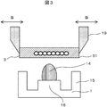
図3と図4を参照して、光モジュールでのファイバブロックの組立工程を説明する。なお、図3と図4は、いずれも図1のA-A’断面図である。図3において、突起16上に液体の接着剤14を供給したあと、ファイバブロック3を微細な位置合せが可能なマニピュレータ19で把持する。xy面内について、基板上に搭載した光素子6とファイバブロック3上のレンズ4の光結合が最良となるようにマニピュレータ19を操作して位置調整する(矢印B)。
Referring to FIG. 3 and FIG. 4, the assembly process of the fiber block in the optical module will be described. 3 and 4 are both A-A 'cross-sectional views of FIG. In FIG. 3, after supplying the liquid adhesive 14 onto the protrusion 16, the fiber block 3 is gripped by a manipulator 19 capable of fine alignment. In the xy plane, the manipulator 19 is operated to adjust the position so that the optical coupling between the optical element 6 mounted on the substrate and the lens 4 on the fiber block 3 is the best (arrow B).
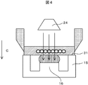
図4において、次に、マニピュレータ19を、基板1の突起15にファイバブロック3の底面31が接触するように-Z方向に移動する(矢印C)。このとき、接着剤14は、基板の突起16とファイバブロック3の間に挟まれた状態となる。ファイバブロック3の上方に設置したUV光源24よりUV光を照射し、UV光がファイバブロック3を通過することで、接着剤14を硬化させる。接着剤14が完全に硬化した後でマニピュレータ19でのファイバブロック3の把持を開放する。UV光を照射により、接着剤14は、硬化収縮に伴う5%程度の体積収縮が起こる。
4, next, the manipulator 19 is moved in the −Z direction so that the bottom surface 31 of the fiber block 3 is in contact with the protrusion 15 of the substrate 1 (arrow C). At this time, the adhesive 14 is sandwiched between the substrate protrusion 16 and the fiber block 3. UV light is irradiated from a UV light source 24 installed above the fiber block 3, and the UV light passes through the fiber block 3 to cure the adhesive 14. After the adhesive 14 is completely cured, the gripping of the fiber block 3 with the manipulator 19 is released. By irradiation with UV light, the adhesive 14 undergoes volume shrinkage of about 5% accompanying cure shrinkage.
接着剤14が硬化収縮を伴って固化するときには、図2に示すように、ファイバブロック3が突起15に直接接触しているためにz方向の接着剤の厚さは収縮できない。これにより、接着剤14の固化後では、接着剤14内部には収縮圧力が内包した状態となっている。
When the adhesive 14 is solidified with curing shrinkage, the thickness of the adhesive in the z direction cannot shrink because the fiber block 3 is in direct contact with the protrusion 15 as shown in FIG. Thereby, after the adhesive 14 is solidified, the shrinkage pressure is included in the adhesive 14.
以上の構造の光モジュール100によれば、温度上昇に伴って、基板1とファイバブロック3との間を接着固定している接着剤14の熱膨張および熱収縮に伴うファイバブロック3のz軸方向の位置ずれを抑制することが可能である。
According to the optical module 100 having the above structure, the z-axis direction of the fiber block 3 due to thermal expansion and thermal contraction of the adhesive 14 that bonds and fixes the substrate 1 and the fiber block 3 with an increase in temperature. Can be suppressed.
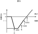
図5を参照して、温度上昇に伴うファイバブロック3のz方向の位置ずれ抑制効果について説明する。図4を参照して説明したように、接着剤14が硬化時の固化後では、接着剤内部には収縮圧力が内包した状態となっている(矢印D)。光モジュール100で温度上昇が起こった場合、接着剤14は、熱膨張により+z方向に伸びる方向に応力が加わる。しかし、接着剤14には収縮応力を内包しているために、温度上昇にしたがって圧縮応力を開放するだけで、膨張することがない(矢印E)。接着剤14の熱膨張率は、50PPM/℃程度である。したがって、収縮応力を完全に開放するためには125℃の温度上昇が必要である。これに対して、光モジュール100の上限温度は、100℃以下であるので、光モジュールの使用温度においては、接着剤には常に収縮応力がかかった状態である。したがって、ファイバブロック3のz方向の高さ変化は発生しない。
Referring to FIG. 5, the effect of suppressing the displacement of the fiber block 3 in the z direction due to the temperature rise will be described. As described with reference to FIG. 4, after the adhesive 14 is solidified at the time of curing, the shrinkage pressure is included in the adhesive (arrow D). When the temperature rises in the optical module 100, the adhesive 14 is stressed in the direction extending in the + z direction due to thermal expansion. However, since the adhesive 14 contains a shrinkage stress, it simply releases the compressive stress as the temperature rises, and does not expand (arrow E). The thermal expansion coefficient of the adhesive 14 is about 50 PPM / ° C. Therefore, a temperature increase of 125 ° C. is necessary to completely release the shrinkage stress. On the other hand, since the upper limit temperature of the optical module 100 is 100 ° C. or lower, the shrinkage stress is always applied to the adhesive at the operating temperature of the optical module. Therefore, the height change of the fiber block 3 in the z direction does not occur.
一方、光モジュールに温度低下が起こった場合、接着剤14は、熱収縮をする。しかし、図2の構造ではファイバクロック3が突起15に接触しているために、基板1上に設置された光素子6との間の光学距離(H_b1-H_b3-H_b4)は変化しない。
On the other hand, when a temperature drop occurs in the optical module, the adhesive 14 undergoes heat shrinkage. However, in the structure of FIG. 2, since the fiber clock 3 is in contact with the protrusion 15, the optical distance (H_b1-H_b3-H_b4) between the optical element 6 installed on the substrate 1 does not change.
次に、xy面内のファイバブロックの位置ずれ抑制効果について説明する。突起16の上面に設けられた接着剤14は、z方向での段差のない平らな接着面32にてファイバプロック3に接着されている。突起15の側面と突起16の側面の間には空気層18があり、突起15の側面には接着剤14が接触していない。温度上昇によって接着剤が膨張した場合、接着剤14の側面は、空気18に接しているために拘束されておらず、自由に膨張することができる。これから、接着剤14は、ファイバブロック3に応力を与えることはない。ファイバブロックの接着面32は、段差のない平らな状態である。このため、接着面32が接着剤14の膨張から受ける力は、接着界面からのせん断応力のみである。接着界面32は、円状をしているために、接着剤界面から受ける力は等方的となり、ファイバブロック3のxy面内に位置ずれを生じさせる応力の合計はキャンセルすることになる。よって、xy面内における位置ずれは発生しない。
Next, the effect of suppressing the displacement of the fiber block in the xy plane will be described. The adhesive 14 provided on the upper surface of the protrusion 16 is bonded to the fiber block 3 with a flat bonding surface 32 having no step in the z direction. There is an air layer 18 between the side surface of the projection 15 and the side surface of the projection 16, and the adhesive 14 is not in contact with the side surface of the projection 15. When the adhesive expands due to the temperature rise, the side surface of the adhesive 14 is not restrained because it is in contact with the air 18 and can expand freely. From this, the adhesive 14 does not apply stress to the fiber block 3. The bonding surface 32 of the fiber block is in a flat state without a step. For this reason, the force that the bonding surface 32 receives from the expansion of the adhesive 14 is only the shear stress from the bonding interface. Since the adhesive interface 32 has a circular shape, the force received from the adhesive interface is isotropic, and the sum of stresses that cause displacement in the xy plane of the fiber block 3 is cancelled. Therefore, no positional deviation occurs in the xy plane.
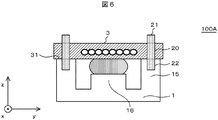
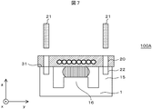
図6と図7を参照して、実施例2の光モジュールを説明する。図6において、光モジュール100Aの基板1には、突起15と突起16に加えて、突起15に勘合穴22が設けられている。
The optical module of Example 2 will be described with reference to FIGS. In FIG. 6, the board 1 of the optical module 100 </ b> A is provided with a fitting hole 22 in the protrusion 15 in addition to the protrusion 15 and the protrusion 16.
一方、ファイバブロック3においても勘合孔20が設けられている。勘合ピン21を勘合孔20と勘合穴22とを両方に通すことで、光素子6とレンズ4の位置合せが可能である。これにより、実施例1の図4と図5に示したようなマニピュレータ19を使わなくても、ファイバブロック3のxy方向の位置合せを簡単に行うことができる。
On the other hand, the fiber block 3 is also provided with a fitting hole 20. The optical element 6 and the lens 4 can be aligned by passing the fitting pin 21 through both the fitting hole 20 and the fitting hole 22. Accordingly, the alignment of the fiber block 3 in the xy direction can be easily performed without using the manipulator 19 as shown in FIGS. 4 and 5 of the first embodiment.
接着剤14は、実施例1に説明したように、突起16の上面とファイバプロック3の接着面32との間に存在する。ファイバブロック底面の接着面はz方向での段差のない平らな状態である。突起15の上面はファイバブロック底面31に直接接触している。これによりファイバブロックのz方向の高さは、H_b1によって決定されることになる。
The adhesive 14 exists between the upper surface of the protrusion 16 and the adhesive surface 32 of the fiber block 3 as described in the first embodiment. The bonding surface on the bottom surface of the fiber block is flat without a step in the z direction. The upper surface of the protrusion 15 is in direct contact with the fiber block bottom surface 31. Thereby, the height of the fiber block in the z direction is determined by H_b1.
以上の実施例2の構造においては、実施例1の図3と図4で説明した組み立て工程にて接着剤14を硬化させることで、接着剤内部に圧縮応力を内包することが可能である。z方向のファイバブロックの位置ずれについては、図5での説明した実施例1と同様である。
In the structure of Example 2 described above, it is possible to include compressive stress inside the adhesive by curing the adhesive 14 in the assembly process described in FIGS. 3 and 4 of Example 1. The positional deviation of the fiber block in the z direction is the same as that of the first embodiment described with reference to FIG.
図7において、勘合ピン21は、取り外しができる方が望ましい。光モジュール100Aは、勘合ピン21を用いてファイバブロック3の位置合せ行い、接着剤14の硬化によって固定した後に勘合ピン21を抜き取ることが可能である。よって、光モジュール100Aは、図7に示すように、勘合ピン21は存在していないが、勘合孔20と勘合穴22は残る。
In FIG. 7, it is desirable that the fitting pin 21 can be removed. The optical module 100 </ b> A can align the fiber block 3 using the fitting pin 21, and can pull out the fitting pin 21 after fixing by fixing the adhesive 14. Therefore, in the optical module 100A, as shown in FIG. 7, the fitting pin 21 does not exist, but the fitting hole 20 and the fitting hole 22 remain.
ファイバブロック3は、勘合ピン21によって位置合せを行い、接着剤14での固定の終了後に勘合ピン21を抜き取るために、位置ずれを起こすことがない。また、勘合ピン21の抜き取り後には温度が変化しても、基板1にxy面内の応力が加わることはない。
実施例2によれば、その製造に於いてマニピュレータの使用が不要な光モジュールを得ることができる。 Thefiber block 3 is aligned with the fitting pin 21, and the fitting pin 21 is pulled out after the fixing with the adhesive 14 is completed. Further, even if the temperature changes after the fitting pin 21 is extracted, no stress in the xy plane is applied to the substrate 1.
According to the second embodiment, an optical module that does not require the use of a manipulator in its manufacture can be obtained.
実施例2によれば、その製造に於いてマニピュレータの使用が不要な光モジュールを得ることができる。 The
According to the second embodiment, an optical module that does not require the use of a manipulator in its manufacture can be obtained.
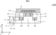
図8を参照して、実施例3の光モジュールを説明する。図8において、光モジュール100Bは、突起15の側面と突起16の側面の間には接着剤23が残っている。この接着剤23の厚さH_sは、突起16の側面高さ(H_b2-H_b3)よりも低い、すなわち、H_s<H_b1の関係がある。
The optical module of Example 3 will be described with reference to FIG. In FIG. 8, in the optical module 100 </ b> B, the adhesive 23 remains between the side surface of the protrusion 15 and the side surface of the protrusion 16. The thickness H_s of the adhesive 23 is lower than the side surface height (H_b2-H_b3) of the protrusion 16, that is, there is a relationship of H_s <H_b1.
このため、接着剤23は、ファイバブロックの底面31に接触することはない。したがって、突起15の上面がファイバブロックの底面31に直接接触している。
Therefore, the adhesive 23 does not contact the bottom surface 31 of the fiber block. Therefore, the upper surface of the protrusion 15 is in direct contact with the bottom surface 31 of the fiber block.
突起15と突起16に囲まれた接着剤23では、温度上昇による接着剤23の熱膨張が発生してもz方向には空気層18があるために、接着剤23が熱膨張しても、ファイバブロック3に加わる応力は実施例1と同じである。xy面内においては、接着剤23は突起15もしくは突起16の側面に応力を加えるが、ファイバブロック3には応力を加えることはない。
実施例3に依れば、図3で説明した接着剤14の塗布量を正確に制御することが不要で、多めに塗布しさえすればよい。 In the adhesive 23 surrounded by the protrusions 15 and 16, even if the thermal expansion of the adhesive 23 due to a temperature rise occurs, the air layer 18 exists in the z direction. The stress applied to the fiber block 3 is the same as in the first embodiment. In the xy plane, the adhesive 23 applies stress to the side surfaces of the protrusions 15 or 16, but does not apply stress to the fiber block 3.
According to the third embodiment, it is not necessary to accurately control the application amount of the adhesive 14 described with reference to FIG.
実施例3に依れば、図3で説明した接着剤14の塗布量を正確に制御することが不要で、多めに塗布しさえすればよい。 In the adhesive 23 surrounded by the
According to the third embodiment, it is not necessary to accurately control the application amount of the adhesive 14 described with reference to FIG.
1…基板、3…ファイバブロック、4…レンズ、5…ミラー、6…光素子、7…IC、8…ファイバ…、9…V溝、10…凹部、11…配線、13…ファイバブロックの端面、14…接着剤、15…突起、16…突起、17…基板厚さ、18…空気層、19…マニピュレータ、20…勘合穴、21…勘合ピン、22…勘合穴…、23…接着剤…、24…UV光源、31…ファイバブロック底面、32…ファイバブロックの接着剤と接触している接着部分、40…光素子、41…はんだ、42…透明樹脂基板、43…導電性パターン、44…アレイレンズ基板、45…レンズホルダ、46…光コネクタ、47…V溝、48…光ファイバ、49…ガイドピン、50…ガイド穴、51…ミラー面、52…IC、53…セラミック基板、54…スルーホール、100…光モジュール。
DESCRIPTION OF SYMBOLS 1 ... Board | substrate, 3 ... Fiber block, 4 ... Lens, 5 ... Mirror, 6 ... Optical element, 7 ... IC, 8 ... Fiber ..., 9 ... V groove, 10 ... Recessed part, 11 ... Wiring, 13 ... End face of fiber block 14 ... adhesive, 15 ... protrusion, 16 ... protrusion, 17 ... substrate thickness, 18 ... air layer, 19 ... manipulator, 20 ... fitting hole, 21 ... fitting pin, 22 ... fitting hole ..., 23 ... adhesive ... , 24 ... UV light source, 31 ... bottom surface of the fiber block, 32 ... adhesive portion in contact with the adhesive of the fiber block, 40 ... optical element, 41 ... solder, 42 ... transparent resin substrate, 43 ... conductive pattern, 44 ... Array lens substrate, 45 ... lens holder, 46 ... optical connector, 47 ... V groove, 48 ... optical fiber, 49 ... guide pin, 50 ... guide hole, 51 ... mirror surface, 52 ... IC, 53 ... ceramic substrate, 54 ... Sul Hall, 100 ... light module.
Claims (9)
- 送信素子または受信素子である光素子と、前記光素子を駆動または前記光素子の出力を増幅する半導体と、前記光素子および前記半導体と電気的に接続された配線基板と、前記光素子と光学的に接続されたファイバブロックと、を含んで構成された光モジュールにおいて、
前記配線基板は、前記ファイバブロックに接する複数の第1の突起と、前記第1の突起と他の前記第1の突起の間に配置され、前記第1の突起より高さの低い第2の突起と、を備え、
前記第2の突起と前記ファイバブロックとは、光硬化性の接着剤で接続されていることを特徴とする光モジュール。 An optical element that is a transmitting element or a receiving element; a semiconductor that drives the optical element or amplifies the output of the optical element; the optical element; a wiring board that is electrically connected to the semiconductor; the optical element and the optical element; An optical module configured to include an optically connected fiber block;
The wiring board is disposed between a plurality of first protrusions in contact with the fiber block, the first protrusion and the other first protrusions, and a second height lower than the first protrusions. A projection, and
The optical module, wherein the second protrusion and the fiber block are connected by a photocurable adhesive. - 請求項1に記載の光モジュールであって、
前記第1の突起の高さをH_b1とし、前記第2の突起の高さをH_b2とするとき、
H_b1/(H_b1-H_b2)>10の関係にあることを特徴とする光モジュール。 The optical module according to claim 1,
When the height of the first protrusion is H_b1, and the height of the second protrusion is H_b2,
An optical module having a relationship of H_b1 / (H_b1-H_b2)> 10. - 請求項1または請求項2に記載の光モジュールであって、
前記第1の突起の第1の側面と前記第2の突起の第2の側面との間に空間を有することを特徴とする光モジュール。 The optical module according to claim 1 or 2, wherein
An optical module comprising a space between a first side surface of the first protrusion and a second side surface of the second protrusion. - 請求項1ないし請求項3のいずれか一つに記載された光モジュールであって、
前記ファイバブロックの底面の前記接着剤に接した部分は、平面であることを特徴とする光モジュール。 An optical module according to any one of claims 1 to 3, wherein
A portion of the bottom surface of the fiber block that is in contact with the adhesive is a flat surface. - 請求項1ないし請求項4のいずれか一つに記載された光モジュールであって、
前記ファイバブロックは、接着剤硬化で用いる波長に対して透過率が10%以上あることを特徴とする光モジュール。 An optical module according to any one of claims 1 to 4, wherein
The optical module is characterized in that the fiber block has a transmittance of 10% or more with respect to a wavelength used for adhesive curing. - 請求項1ないし請求項5のいずれか一つに記載された光モジュールであって、
前記ファイバブロックは、基板上に設置した光素子で使用する波長帯域において、透過率が70%以上であることを特徴とする光モジュール。 An optical module according to any one of claims 1 to 5, comprising:
An optical module characterized in that the fiber block has a transmittance of 70% or more in a wavelength band used by an optical element placed on a substrate. - 請求項1ないし請求項6のいずれか一つに記載された光モジュールであって、
前記第2の突起の接着面の形状が円または回転対称性の高い多角形であることを特徴とする光モジュール。 An optical module according to any one of claims 1 to 6, comprising:
The optical module according to claim 2, wherein the bonding surface of the second protrusion is a circle or a polygon having high rotational symmetry. - 請求項1ないし請求項7のいずれか一つに記載された光モジュールであって、
前記第1の突起の前記第1の側面と前記第2の突起の前記第2の側面との間に第2の接着剤があり、
前記第2の接着剤の高さをH_sとし、H_s<H_b2の関係にあることを特徴とする光モジュール。 An optical module according to any one of claims 1 to 7,
There is a second adhesive between the first side of the first projection and the second side of the second projection;
The optical module is characterized in that the height of the second adhesive is H_s and H_s <H_b2. - 送信素子または受信素子である光素子と、前記光素子を駆動または前記光素子の出力を増幅する半導体と、前記光素子および前記半導体と電気的に接続された配線基板と、前記光素子と光学的に接続されたファイバブロックと、を含んで構成された光モジュールの製造方法において、
前記ファイバブロックに接する複数の第1の突起と、前記第1の突起と他の前記第1の突起の間に配置され、前記第1の突起より高さの低い第2の突起と、を備えた前記配線基板を準備するステップと、
前記第2の突起に光硬化性の接着剤を塗布するステップと、
前記配線基板と、前記ファイバブロックとを位置決めするステップと、
照射光を前記ファイバブロックの上面より照射し、前記ファイバブロックの内部を透過した前記照射光によって、前記接着剤を固化するステップと、を含む光モジュールの製造方法。 An optical element that is a transmitting element or a receiving element; a semiconductor that drives the optical element or amplifies the output of the optical element; the optical element; a wiring board that is electrically connected to the semiconductor; the optical element and the optical element; In the manufacturing method of the optical module comprised including the optically connected fiber block,
A plurality of first protrusions in contact with the fiber block; and a second protrusion disposed between the first protrusion and the other first protrusion and having a height lower than that of the first protrusion. Preparing the wiring board;
Applying a photo-curable adhesive to the second protrusion;
Positioning the wiring board and the fiber block;
Irradiating irradiation light from the upper surface of the fiber block, and solidifying the adhesive by the irradiation light transmitted through the inside of the fiber block.
Priority Applications (1)
| Application Number | Priority Date | Filing Date | Title |
|---|---|---|---|
| PCT/JP2013/065632 WO2014196043A1 (en) | 2013-06-05 | 2013-06-05 | Optical module and method for manufacturing optical module |
Applications Claiming Priority (1)
| Application Number | Priority Date | Filing Date | Title |
|---|---|---|---|
| PCT/JP2013/065632 WO2014196043A1 (en) | 2013-06-05 | 2013-06-05 | Optical module and method for manufacturing optical module |
Publications (1)
| Publication Number | Publication Date |
|---|---|
| WO2014196043A1 true WO2014196043A1 (en) | 2014-12-11 |
Family
ID=52007719
Family Applications (1)
| Application Number | Title | Priority Date | Filing Date |
|---|---|---|---|
| PCT/JP2013/065632 WO2014196043A1 (en) | 2013-06-05 | 2013-06-05 | Optical module and method for manufacturing optical module |
Country Status (1)
| Country | Link |
|---|---|
| WO (1) | WO2014196043A1 (en) |
Cited By (2)
| Publication number | Priority date | Publication date | Assignee | Title |
|---|---|---|---|---|
| WO2020088011A1 (en) * | 2018-11-02 | 2020-05-07 | 青岛海信宽带多媒体技术有限公司 | Receiver optical subassembly and optical module |
| CN114522892A (en) * | 2021-12-31 | 2022-05-24 | 武汉英飞光创科技有限公司 | Coupling method and device for optical module with AWG |
Citations (4)
| Publication number | Priority date | Publication date | Assignee | Title |
|---|---|---|---|---|
| JPH10325917A (en) * | 1997-05-26 | 1998-12-08 | Matsushita Electric Ind Co Ltd | Optical receiver and its manufacture |
| JP2005062645A (en) * | 2003-08-19 | 2005-03-10 | Toppan Printing Co Ltd | Optical connection structure body and its manufacturing method |
| JP2006011046A (en) * | 2004-06-25 | 2006-01-12 | Sony Corp | Optical waveguide and its optical waveguide module, and optical transmission mode |
| JP2009198804A (en) * | 2008-02-21 | 2009-09-03 | Sony Corp | Optical module and optical waveguide |
-
2013
- 2013-06-05 WO PCT/JP2013/065632 patent/WO2014196043A1/en active Application Filing
Patent Citations (4)
| Publication number | Priority date | Publication date | Assignee | Title |
|---|---|---|---|---|
| JPH10325917A (en) * | 1997-05-26 | 1998-12-08 | Matsushita Electric Ind Co Ltd | Optical receiver and its manufacture |
| JP2005062645A (en) * | 2003-08-19 | 2005-03-10 | Toppan Printing Co Ltd | Optical connection structure body and its manufacturing method |
| JP2006011046A (en) * | 2004-06-25 | 2006-01-12 | Sony Corp | Optical waveguide and its optical waveguide module, and optical transmission mode |
| JP2009198804A (en) * | 2008-02-21 | 2009-09-03 | Sony Corp | Optical module and optical waveguide |
Cited By (2)
| Publication number | Priority date | Publication date | Assignee | Title |
|---|---|---|---|---|
| WO2020088011A1 (en) * | 2018-11-02 | 2020-05-07 | 青岛海信宽带多媒体技术有限公司 | Receiver optical subassembly and optical module |
| CN114522892A (en) * | 2021-12-31 | 2022-05-24 | 武汉英飞光创科技有限公司 | Coupling method and device for optical module with AWG |
Similar Documents
| Publication | Publication Date | Title |
|---|---|---|
| US10466433B2 (en) | Optical module including silicon photonics chip and coupler chip | |
| JP6029115B2 (en) | Optical device, optical connector assembly, and optical connection method | |
| US8827572B2 (en) | Side coupling optical fiber assembly and fabrication method thereof | |
| JP4704126B2 (en) | Optical module | |
| US9316799B2 (en) | Optical module and fabrication method | |
| JP4690963B2 (en) | Manufacturing method of multi-channel optical module | |
| US9541715B2 (en) | Optical module, manufacturing method of optical module, and optical device | |
| US7627210B2 (en) | Manufacturing method of optical-electrical substrate and optical-electrical substrate | |
| JP7117133B2 (en) | Optical subassembly, manufacturing method thereof, and optical module | |
| US8615149B2 (en) | Photonics chip with efficient optical alignment and bonding and optical apparatus including the same | |
| JP5323646B2 (en) | Hybrid integrated optical module | |
| JP2009198804A (en) | Optical module and optical waveguide | |
| JP2011095295A (en) | Optical fiber block of optical module and method of manufacturing the same | |
| JP2007072007A (en) | Optical waveguide module | |
| JP5400421B2 (en) | Optical device and manufacturing method thereof | |
| WO2014196043A1 (en) | Optical module and method for manufacturing optical module | |
| JP2013057720A (en) | Optical module | |
| US10073226B2 (en) | Method for coupling an optical fiber to an optical or optoelectronic component | |
| JP2018004830A (en) | High heat-resistant optical fiber module and manufacture method of the same | |
| JP4609375B2 (en) | Optical wiring member manufacturing method and optical wiring member | |
| JP2006120781A (en) | Photoelectric conversion module | |
| JP2006133811A (en) | Optical fiber transmission/reception module | |
| JP2011095294A (en) | Optical module | |
| JP2020008813A (en) | Optical module | |
| KR101175300B1 (en) | Optical module and method for fabricating the same |
Legal Events
| Date | Code | Title | Description |
|---|---|---|---|
| 121 | Ep: the epo has been informed by wipo that ep was designated in this application |
Ref document number: 13886570 Country of ref document: EP Kind code of ref document: A1 |
|
| NENP | Non-entry into the national phase |
Ref country code: DE |
|
| 122 | Ep: pct application non-entry in european phase |
Ref document number: 13886570 Country of ref document: EP Kind code of ref document: A1 |
|
| NENP | Non-entry into the national phase |
Ref country code: JP |