WO2014097488A1 - 半導体装置 - Google Patents
半導体装置 Download PDFInfo
- Publication number
- WO2014097488A1 WO2014097488A1 PCT/JP2012/083346 JP2012083346W WO2014097488A1 WO 2014097488 A1 WO2014097488 A1 WO 2014097488A1 JP 2012083346 W JP2012083346 W JP 2012083346W WO 2014097488 A1 WO2014097488 A1 WO 2014097488A1
- Authority
- WO
- WIPO (PCT)
- Prior art keywords
- pad
- voltage
- gate
- semiconductor device
- excessive current
- Prior art date
- Legal status (The legal status is an assumption and is not a legal conclusion. Google has not performed a legal analysis and makes no representation as to the accuracy of the status listed.)
- Ceased
Links
Images



Classifications
-
- H—ELECTRICITY
- H03—ELECTRONIC CIRCUITRY
- H03K—PULSE TECHNIQUE
- H03K17/00—Electronic switching or gating, i.e. not by contact-making and –breaking
- H03K17/51—Electronic switching or gating, i.e. not by contact-making and –breaking characterised by the components used
- H03K17/56—Electronic switching or gating, i.e. not by contact-making and –breaking characterised by the components used by the use, as active elements, of semiconductor devices
- H03K17/567—Circuits characterised by the use of more than one type of semiconductor device, e.g. BIMOS, composite devices such as IGBT
-
- H—ELECTRICITY
- H10—SEMICONDUCTOR DEVICES; ELECTRIC SOLID-STATE DEVICES NOT OTHERWISE PROVIDED FOR
- H10D—INORGANIC ELECTRIC SEMICONDUCTOR DEVICES
- H10D64/00—Electrodes of devices having potential barriers
- H10D64/20—Electrodes characterised by their shapes, relative sizes or dispositions
- H10D64/27—Electrodes not carrying the current to be rectified, amplified, oscillated or switched, e.g. gates
- H10D64/311—Gate electrodes for field-effect devices
- H10D64/411—Gate electrodes for field-effect devices for FETs
- H10D64/511—Gate electrodes for field-effect devices for FETs for IGFETs
-
- H—ELECTRICITY
- H10—SEMICONDUCTOR DEVICES; ELECTRIC SOLID-STATE DEVICES NOT OTHERWISE PROVIDED FOR
- H10W—GENERIC PACKAGES, INTERCONNECTIONS, CONNECTORS OR OTHER CONSTRUCTIONAL DETAILS OF DEVICES COVERED BY CLASS H10
- H10W20/00—Interconnections in chips, wafers or substrates
- H10W20/40—Interconnections external to wafers or substrates, e.g. back-end-of-line [BEOL] metallisations or vias connecting to gate electrodes
- H10W20/41—Interconnections external to wafers or substrates, e.g. back-end-of-line [BEOL] metallisations or vias connecting to gate electrodes characterised by their conductive parts
- H10W20/43—Layouts of interconnections
-
- H—ELECTRICITY
- H10—SEMICONDUCTOR DEVICES; ELECTRIC SOLID-STATE DEVICES NOT OTHERWISE PROVIDED FOR
- H10W—GENERIC PACKAGES, INTERCONNECTIONS, CONNECTORS OR OTHER CONSTRUCTIONAL DETAILS OF DEVICES COVERED BY CLASS H10
- H10W72/00—Interconnections or connectors in packages
- H10W72/50—Bond wires
- H10W72/541—Dispositions of bond wires
- H10W72/5445—Dispositions of bond wires being orthogonal to a side surface of the chip, e.g. parallel arrangements
Definitions
- a semiconductor device including a gate region is disclosed.
- a semiconductor device in which the resistance between the emitter region and the collector region or between the source region and the drain region is changed by adjusting the voltage applied to the gate region. For example, in the case of an IGBT, by applying a voltage to the gate region, the resistance between the emitter and the collector is lowered, and a current flows between the emitter and the collector. Alternatively, in the case of a MOS, by applying a voltage to the gate region, the resistance between the source and the drain decreases, and a current flows between the source and the drain.
- the gate region in this specification is sometimes referred to as a base region.
- the above semiconductor device may constitute an inverter that controls the current supplied to the motor.
- the inverter includes a parallel circuit in which a plurality of series circuits in which an upper semiconductor device and a lower semiconductor device are connected in series are connected in parallel. In this case, for example, when an abnormality occurs in which the motor coil is short-circuited, an excessive current may flow in the semiconductor device. If the inverter is normal, both the upper semiconductor device and the lower semiconductor device are not turned on at the same time. However, if an abnormality occurs in which both are turned on simultaneously, an excessive current flows in the semiconductor device.
- a lead frame or a bus bar is joined to a surface electrode formed on the surface of a semiconductor device. According to the structure, it is expected that heat generated in the semiconductor device can be transferred to the lead frame or the like via the surface electrode, and the semiconductor device can be protected from overheating.
- This specification discloses a technique for solving a phenomenon in which a different phenomenon occurs depending on a place in a semiconductor device and a problem occurs in a specific place due to the phenomenon.
- the present technology is directed to a semiconductor device in which a gate region extends along the surface of a semiconductor substrate.
- the gate region here is a region formed in a part of the semiconductor substrate or a region formed in addition to the semiconductor substrate and formed of a semiconductor material with enhanced conductivity.
- Some semiconductor devices have a gate region extending along the surface of the semiconductor substrate when the semiconductor substrate is viewed in plan.
- an IGBT is known in which a plurality of linearly extending gate regions are arranged in parallel over a wide range on a substrate.
- a gate wiring for transmitting a voltage to be applied to the gate region is required, a pad conducting to the gate wiring is required, and the pad is disposed on the surface of the semiconductor substrate.
- the pad and gate wiring are made of a metal material.
- a portion formed of a metal material is referred to as a gate wiring, and a region formed of a semiconductor material with increased conductivity is referred to as a gate region. .
- the gate region extends along the surface of the substrate, and is connected to the gate wiring at two or more locations in the gate region. It is formed. Further, when the position connecting the gate region and the first gate wiring is the first connection position, and the position connecting the gate region and the second gate wiring is the second connection position, the first connection is established. The position and the second connection position are set at different positions on the substrate.
- the above semiconductor device includes two or more pads (for example, a first pad and a second pad). Therefore, a pad for transmitting the gate voltage can be selected.
- a pad for transmitting the gate voltage can be selected.
- a connection position between the first gate line extending from the first pad and the gate region is a first connection position
- a connection position between the second gate line extending from the second pad and the gate region is a second connection position.
- the same gate region is also connected to the first pad via the first connection position, and is also connected to the second pad via the second connection position.
- a position close to the first connection position and far from the second connection position is defined as a first position
- a position far from the first connection position and close to the second connection position is defined as a second position.
- the first pad is selected and an on-voltage is applied. In this case, the first position close to the first connection position turns on early, and the second position far from the first connection position turns on late.
- (1b) Select the second pad and apply the ON voltage. In that case, the second position close to the second connection position turns on early, and the first position far from the second connection position turns on late.
- (2a) Select the first pad and apply an off voltage. In that case, the first position close to the first connection position turns off early, and the second position far from the first connection position turns off late.
- the disadvantage is caused by selecting a pad that transmits the gate voltage. It can be prevented from occurring.
- the pad that transmits the gate voltage can be selected from two or more pads, various selections are possible. For example, it may be effective to switch the pad to which the gate voltage is applied between when the on voltage is applied and when the off voltage is applied. In some cases, it is effective to switch the pad to which the gate voltage is applied depending on the period in which an excessive current has not been detected in the semiconductor device. In particular, it may be effective to switch the pad to which the off voltage is applied.
- the problem that the peripheral part easily overheats, or conversely, the problem that the central part easily overheats is dealt with. be able to.
- overheating is likely to occur in the peripheral portion, it is effective to transmit an on voltage to the first pad and transmit an off voltage to the second pad. That is, when “1a and 2b” in FIG. 1 is employed, it is possible to cope with a phenomenon in which overheating tends to occur in the peripheral portion where the second connection position is arranged.
- the first connection position is located at the center of the semiconductor substrate. It is effective to dispose the second connection position on the periphery of the semiconductor substrate and transmit the off voltage to the second pad.
- the temperature rise that occurs when an excessive current flows through the semiconductor device is extremely fast, and it is effective to advance the off timing in the peripheral portion by transmitting the off voltage to the second pad. Even in the above case, the effect of preventing overheating is high even if the time difference that the off timing when transmitting the off voltage to the second pad is advanced is small compared to the off timing when transmitting the off voltage to the first pad.
- a technique is also effective in which an off-voltage is transmitted to the first pad during a period when no excessive current flows through the semiconductor device, and the off-voltage is transmitted to the second pad when it is detected that an excessive current has flowed through the semiconductor device. .
- it may be effective to transmit the on-voltage to the second pad and transmit the off-voltage to the first pad.
- it is useful to communicate both.
- a technique for preventing overheating by transmitting an off voltage to the second pad when it is detected that an excessive current flows in the semiconductor device is useful.
- a first connection position where the gate region and the first gate wiring are conductive is arranged in the center of the substrate, and a second connection position where the gate region and the second gate wiring are conductive is arranged in the peripheral portion of the substrate. It is possible to set a time difference between the on-timing in the central part and the on-timing in the peripheral part, or to set a time difference between the off-timing in the central part and the off-timing in the peripheral part. It is possible to cope with a case where inconvenience occurs in the central part or the peripheral part.
- the peripheral portion When the on-voltage is applied to the first pad and the off-voltage is transmitted to the second pad, the peripheral portion can be prevented from overheating even in an environment where the peripheral portion is likely to overheat. In addition, when an excessive current is generated, it is possible to suppress heat generation in a peripheral portion that is likely to be overheated when the excessive current is generated, and an effect of protecting the semiconductor device from overheating can be obtained.
- the off-voltage is transmitted to the first pad, and when the excessive current is detected, the off-voltage is transmitted to the second pad.
- both the on voltage and the off voltage may be transmitted to the first pad.
- the ON period during which no excessive current is detected can be made uniform at the central portion and the peripheral portion.
- an on voltage may be applied to the second pad and an off voltage may be applied to the first pad.
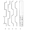
- An event that occurs by selecting a pad to which a gate voltage is applied will be described.
- the circuit structure of an Example and the surface of a semiconductor substrate are shown typically.
- the surface of a semiconductor device is shown typically.
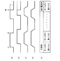
- the pad selection method according to the first embodiment and the events caused thereby will be described.
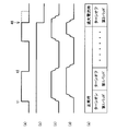
- the pad selection method according to the second embodiment and the events caused thereby will be described.
- a pad selection method according to the third embodiment and events caused thereby will be described.
- the surface of the semiconductor substrate of another Example is typically shown.
- the pad that is connected to the gate wiring on the central side of the semiconductor substrate is referred to as the first pad, and the connection position to the gate region is connected to the gate wiring on the peripheral side of the semiconductor substrate.
- This pad is called the second pad.
- Feature 1 The first pad is selected at the application timing of the on signal, and the second pad is selected at the application timing of the off signal.
- Feature 1A While the gate voltage adjustment circuit is outputting the ON voltage, the first pad is floated and the second pad is connected to the gate voltage adjustment circuit.
- Feature 1B While the gate voltage adjustment circuit outputs an off-voltage, the first pad is connected to the gate voltage adjustment circuit and the second pad is floated.
- Feature 2 During a period in which no excessive current is detected, the second pad is selected at the application timing of the on signal, and the first pad is selected at the application timing of the off signal. When an excessive current is detected, the second pad is selected.
- Feature 2A While the gate voltage adjustment circuit outputs the on-voltage, the first pad is connected to the gate voltage adjustment circuit, and the second pad is floated.
- Feature 2B While the gate voltage adjustment circuit is outputting the off voltage, the first pad is floated and the second pad is connected to the gate voltage adjustment circuit.
- Feature 3 The first pad is selected during a period in which no excessive current is detected. When an excessive current is detected, the second pad is selected. Characteristic 3A: When an excessive current is detected, the gate voltage adjustment circuit outputs an off voltage.
- reference numeral 36 indicates the semiconductor device of the first embodiment.
- a first pad 22 and a second pad 26 are formed on the surface of the substrate 32.
- the first gate wiring 24 is electrically connected to the first pad 22.
- the first gate wiring 24 is formed by a horizontal portion 24 a connecting the center position of the substrate 32 and the first pad 22, and two oblique portions 24 b and 24 c extending in the diagonal direction of the substrate 32.
- the second gate wiring 28 is electrically connected to the second pad 26.
- the second gate wiring 28 extends along the outer periphery of the substrate 32.
- Reference numeral 34 is a guard ring for increasing the breakdown voltage in the peripheral portion of the semiconductor device.
- the semiconductor device 36 is an IGBT, and an IGBT structure is formed in a region inside the guard ring 34.
- the second gate wiring 28 makes a round around the outside of the region where the IGBT is formed.
- Reference numbers 30a, 30b, 30c and the like indicate gate regions. For clarity of illustration, reference numerals 30a, 30b, and 30c are given only to some gate regions. Each of the illustrated thin lines represents a gate region extending along the surface of the substrate 32.
- the gate regions 30a, 30b, 30c and the like extend linearly along the surface of the substrate 32 and are arranged in parallel to each other. In FIG. 2, for the sake of clarity of illustration, the interval between adjacent gate regions is enlarged. In practice, the spacing between parallel gate regions is much narrower.
- the gate regions 30 a, 30 b, 30 c, etc. are widely spread in the region inside the guard ring 34, and the IGBT is formed in a wide range in the region inside the guard ring 34.
- Each gate region is connected to both the first gate wiring 24 and the second gate wiring 28.
- the gate region 30 c is connected to the skewed portion 24 c of the first gate wiring 24 and the second gate wiring 28.
- a plurality of gate regions are collectively referred to as a gate region 30. Since the second gate wiring 28 extends along the outer periphery of the substrate 32, the second connection position connecting the gate region 30 and the second gate wiring 28 is arranged at a position along the outer periphery of the substrate 32. ing.
- the first gate wiring 24 is formed in a range surrounded by the second gate wiring 28, the first connection position connecting the gate region 30 and the first gate wiring 24 is the second connection position. It is distributed in the area inside the connection position.
- the first connection positions are distributed in a region 42 (see FIG. 3) from the center of the substrate 32, and the second connection positions are distributed in a region 40 located around the substrate 32.
- FIG. 2 shows a structure inside the protective film formed on the surface of the semiconductor substrate 32, and the surface of the semiconductor substrate 32 is actually covered with the protective film.
- FIG. 3 is a view of the surface of the semiconductor device 36, and a region excluding the first pad 22 and the second pad 26 is covered with a protective film 44.
- An emitter electrode 38 is formed on the surface of the protective film 44.
- the emitter electrode 38 is electrically connected to an emitter region formed in the semiconductor substrate 32.
- the emitter electrode 38 and the gate region 30 are insulated by a protective film 44.
- a collector electrode (not shown) is formed on the back surface of the semiconductor substrate 32.
- the distribution area 42 of the first connection position and the distribution area 40 of the second connection position are indicated by broken lines.
- the collector electrode on the back surface is soldered to another substrate
- the emitter electrode 38 on the front surface is soldered to the bus bar
- the pads 22 and 26 are connected to the gate voltage adjusting circuit.
- the semiconductor device 36 has such a characteristic that the peripheral portion easily overheats when an excessive current flows.
- the gate region 30 is provided with two pads for transmitting the gate voltage, and the above problem is addressed by utilizing the characteristic that the pad for transmitting the gate voltage can be selected.
- a terminal 2 indicates a terminal for inputting a signal voltage output from another device.
- a high voltage is input to the terminal 2 during a period in which the semiconductor device (IGBT) 36 is turned on, and a low voltage is input during the period in which the semiconductor device 36 is turned off.
- the transistor 4 constituting the cMOS circuit 8 is turned on, the transistor 6 is turned off, and the voltage at the position indicated by reference numeral 14 rises to the VG voltage.
- the rising speed is adjusted by the on-resistance 10.
- the transistor 4 constituting the cMOS circuit 8 is turned off and the transistor 6 is turned on, and the voltage at the position indicated by reference numeral 14 drops to the ground voltage.
- the descending speed is adjusted by the off-resistance 12.
- the gate voltage adjusting circuit 1 is composed of the cMOS circuit 8 and the like.
- a pad for transmitting a gate voltage output from the gate voltage adjusting circuit 1 is provided between the position indicated by reference numeral 14 and the first pad 22 and between the position indicated by reference numeral 14 and the second pad 26.
- a circuit 15 for selection is added.
- a high voltage is input to the terminal 20 while the first pad 22 is connected to the gate voltage adjusting circuit 1 and the second pad 26 is floated, and the second pad 26 is connected to the gate voltage adjusting circuit 1 to be connected to the first voltage.
- a low voltage is input while the pad 22 is floating.
- FIG. 4A illustrates the input voltage at the terminal 2.
- FIG. 4B shows the input voltage at the terminal 20.
- (a) and (b) are compared, the timing is adjusted so that the first pad 22 is selected and the second pad 26 is floated prior to the timing t1 when the ON signal is input. Prior to the timing t2 when the off signal is input, the second pad 26 is selected and the first pad 22 is floated.
- (E) summarizes the relationship.
- (C) shows the gate voltage of the IGBT formed in the central part of the substrate 32
- (d) shows the gate voltage of the IGBT formed in the peripheral part of the substrate 32.
- the IGBT formed in the central portion is turned on early, and the IGBT formed in the peripheral portion is turned on with a delay.
- the off voltage is transmitted to the second pad 26, the IGBT formed in the central portion is turned off with a delay, and the IGBT formed in the peripheral portion is turned off early.
- the IGBT generates heat during the on period. According to this embodiment, heat generation at the peripheral portion can be suppressed, and the problem of overheating at the peripheral portion can be dealt with.
- a low voltage is input to the terminal 2 and a low voltage is also input to the terminal 20.
- FIG. 4B shows an enlarged view of the on-timing time difference and off-timing time difference between the central portion and the peripheral portion.
- the actual time difference is small, and the phenomenon that depends on the average value with respect to the time has no practical influence because the central on-period is long and the peripheral off-period is short.
- a time difference affects a transient event such as a temperature rise phenomenon when an excessive current flows.
- the peripheral portion is likely to overheat due to an excessive current, it is effective to turn off the peripheral portion earlier than the central portion.
- FIG. 5A illustrates the input voltage at the terminal 2.
- FIG. 5B shows the input voltage at the terminal 20.
- An arrow 46 illustrates the moment when an excessive current flows. While the excessive current is not flowing, it is clear that when comparing (a) and (b), the second pad 26 is selected and the first pad 22 is floated prior to the timing t1 when the ON signal is input. Has been. Further, prior to the timing t2 when the off signal is input, the first pad 22 is selected and the second pad 26 is floated. When an excessive current flows, the voltage input to the terminal 2 becomes low and the voltage input to the terminal 20 also becomes low as indicated by the position of the arrow 46. When an excessive current flows, an off signal is transmitted to the second pad 26.
- E summarizes the relationship.
- (C) shows the gate voltage of the IGBT formed in the central part of the substrate 32
- (d) shows the gate voltage of the IGBT formed in the peripheral part of the substrate 32. Since the on-voltage is transmitted to the second pad 26, the IGBT formed in the peripheral portion is turned on early, and the IGBT formed in the central portion is turned off with a delay. On the other hand, since the off voltage is transmitted to the first pad 22, the IGBT formed in the central portion is turned off early, and the IGBT formed in the peripheral portion is turned off with a delay. According to the present embodiment, heat generation at the central portion can be suppressed, and the problem of overheating at the central portion can be dealt with.
- FIG. 6A illustrates the input voltage at the terminal 2.
- FIG. 6B shows the input voltage at the terminal 20.
- An arrow 46 illustrates the moment when an excessive current flows. While the excessive current is not flowing, it is apparent from (b) that the first pad 22 is selected and the second pad 26 is floated. When an excessive current flows, the voltage input to the terminal 2 becomes low and the voltage input to the terminal 20 also becomes low as indicated by the position of the arrow 46. When an excessive current flows, an off signal is transmitted to the second pad 26.
- (E) summarizes the relationship.
- (C) shows the gate voltage of the IGBT formed in the central part of the substrate 32
- (d) shows the gate voltage of the IGBT formed in the peripheral part of the substrate 32.
- the IGBT formed in the central portion is turned on earlier and turned off earlier.
- the IGBT formed in the peripheral part is turned on with a delay and turned off with a delay.
- the on period in the central part and the on period in the peripheral part can be made uniform.
- the value of the on-timing time difference / single on-period ratio or the off-timing time difference / single off-period ratio depending on the location in the semiconductor device is small. Choosing a pad has a low impact on an event where an integrated effect appears over a single on period or a single off period. On the other hand, the temperature rise phenomenon when an excessive current flows is fast, and the off timing when the off voltage is transmitted to the second pad is lower than the off timing when the off voltage is transmitted to the first pad. Although the time difference to be advanced is small, it is effective for the problem that the peripheral portion is likely to overheat when an excessive current flows.
- FIG. 7 illustrates another example of the first pad 22A, the second pad 26A, the first gate wiring 24A, the second gate wiring 28A, and the gate region 30A. Even in this semiconductor device, a phenomenon equivalent to that of the semiconductor device described above can be obtained.
- Gate voltage adjustment circuit 2 Terminal 4: Transistor 6: Transistor 8: cMOS 10: ON resistance 12: OFF resistance 15: Pad selection circuit 16: Transistor 18: Transistor 20: Terminal 22: First pad 24: First gate wiring 26: Second pad 28: Second gate wiring 30: Gate region 32: Substrate 34: Guard ring 36: Semiconductor device 38: Emitter electrode 40: Second connection position distribution region 42: First connection position distribution region 44: Protective film 46: Overcurrent generation timing
Landscapes
- Semiconductor Integrated Circuits (AREA)
- Physics & Mathematics (AREA)
- Geometry (AREA)
- Power Conversion In General (AREA)
Abstract
Description
ここでいうゲート領域は、半導体基板の一部に形成されている領域、あるいは、半導体基板に付加して形成されている領域であって、導電性が高められた半導体材料で形成されている領域をいう。半導体装置のなかには、半導体基板を平面視した場合に、半導体基板の表面に沿ってゲート領域が伸びているものがある。例えば、直線的に伸びているゲート領域の複数本が、基板上の広い範囲に亘って平行に配置されているIGBTが知られている。この種の半導体装置では、ゲート領域に印加する電圧を伝達するためのゲート配線が必要とされ、そのゲート配線に導通するパッドが必要とされ、そのパッドを半導体基板の表面に配置していることがある。パッドとゲート配線は金属材料で形成されている。本明細書では、パッドに導通している導電性の部分のうち、金属材料で形成されている部分をゲート配線といい、導電性が高められた半導体材料で形成されている領域をゲート領域という。
また、第1接続位置に近くて第2接続位置から遠い位置を第1位置とし、第1接続位置から遠くて第2接続位置から近い位置を第2位置とする。その場合、ゲート領域ではゲート電圧伝播速度が遅いことから、ゲート電圧を印加するパッドを選択することによって、図1に示す現象が生じる。
(1a)第1パッドを選択してオン電圧を印加する。その場合、第1接続位置に近い第1位置では早くオンし、第1接続位置から遠い第2位置では遅れてオンする。
(1b)第2パッドを選択してオン電圧を印加する。その場合、第2接続位置に近い第2位置では早くオンし、第2接続位置から遠い第1位置では遅れてオンする。
(2a)第1パッドを選択してオフ電圧を印加する。その場合、第1接続位置に近い第1位置では早くオフし、第1接続位置から遠い第2位置では遅れてオフする。
(2b)第2パッドを選択してオフ電圧を印加する。その場合、第2接続位置に近い第2位置では早くオフし、第2接続位置から遠い第1位置では遅れてオフする。
周辺部で過熱しやすい場合は、第1パッドにオン電圧を伝達して第2パッドにオフ電圧を伝達するのが有効である。すなわち、図1の「1aと2b」を採用すると、第2接続位置が配置されている周辺部で過熱しやすい現象に対処することができる。
半導体装置に過大電流が流れていない期間は、第2パッドにオン電圧を伝達して第1パッドにオフ電圧を伝達するのが有効な場合もあれば、第1パッドにオン電圧とオフ電圧の双方を伝達するのが有効な場合もある。いずれの場合でも、半導体装置に過大電流が流れたことを検出した時に、第2パッドにオフ電圧を伝達することによって、過熱を防止する技術が有用である。
過大電流が検出されない間は、オン電圧とオフ電圧の両方を第1パッドに伝達するようにしてもよい。過大電流が検出されない間のオン期間を、中央部と周辺部で揃えることができる。これに代えて、過大電流が検出されない間は、第2パッドにオン電圧を印加して第1パッドにオフ電圧を印加してもよい。中央部で過熱し易い場合には、上記によって中央部での過熱を防止できる。
特徴1:オン信号の印加タイミングでは第1パッドを選択しておき、オフ信号の印加タイミングでは第2パッドを選択しておく。
特徴1A:ゲート電圧調整回路がオン電圧を出力している間に、第1パッドをフローティングして、第2パッドをゲート電圧調整回路に接続する。
特徴1B:ゲート電圧調整回路がオフ電圧を出力している間に、第1パッドをゲート電圧調整回路に接続して、第2パッドをフローティングする。
特徴2:過大電流が検出されない期間は、オン信号の印加タイミングでは第2パッドを選択しておき、オフ信号の印加タイミングでは第1パッドを選択しておく。過大電流が検出された時に、第2パッドを選択する。
特徴2A:ゲート電圧調整回路がオン電圧を出力している間に、第1パッドをゲート電圧調整回路に接続して、第2パッドをフローティングする。
特徴2B:ゲート電圧調整回路がオフ電圧を出力している間に、第1パッドをフローティングして、第2パッドをゲート電圧調整回路に接続する。
特徴3:過大電流が検出されない期間は、第1パッドを選択しておく。過大電流が検出された時に、第2パッドを選択する。
特徴3A:過大電流を検出した時に、ゲート電圧調整回路がオフ電圧を出力する。
ゲート領域30a,30b,30c等は、基板32の表面に沿って直線的に伸びており、相互に平行に配置されている。図2では、図示の明瞭化のために、隣接するゲート領域の間隔を拡大して図示している。実際には、平行するゲート領域間の間隔はもっと狭い。ゲート領域30a,30b,30c等は、ガードリング34の内側の領域に広く広がっており、ガードリング34の内側の領域の広い範囲にIGBTを形成している。
図3では、第1接続位置の分布領域42と、第2接続位置の分布領域40を破線で示している。
本実施例では、ゲート領域30にゲート電圧を伝達するパッドを2個備えており、ゲート電圧を伝達するパッドを選択できるという特性を利用して、上記問題に対処する。
端子20には、第1パッド22をゲート電圧調整回路1に接続して第2パッド26をフローティングする間はハイ電圧が入力され、第2パッド26をゲート電圧調整回路1に接続して第1パッド22をフローティングする間はロー電圧が入力される。端子20にハイ電圧が入力すると、トランジスタ16がオンしてトランジスタ18がオフし、ゲート電圧調整回路1の出力電圧が第1パッド22に入力され、第2パッド26はフローティングされる。端子20にロー電圧が入力すると、トランジスタ16がオフしてトランジスタ18がオンし、ゲート電圧調整回路1の出力電圧が第2パッド26に入力され、第1パッド22はフローティングされる。
(c)は、基板32の中央部に形成されているIGBTのゲート電圧を示し、(d)は基板32の周辺部に形成されているIGBTのゲート電圧を示している。オン電圧は第1パッド22に伝達されるために、中央部に形成されているIGBTは早くオンし、周辺部に形成されているIGBTは遅れてオンする。その一方において、オフ電圧は第2パッド26に伝達されるために、中央部に形成されているIGBTは遅れてオフし、周辺部に形成されているIGBTは早くオフする。IGBTはオン期間に発熱する。本実施例によると、周辺部での発熱を抑制することができ、周辺部で過熱する問題に対処することができる。
上記実施例では、半導体装置36に過大電流が流れたことが検出されたときには、端子2にロー電圧が入力され、端子20にもロー電圧が入力される。この結果、最初に周辺部のIGBTがオフする。過大電流が流れる時に周辺部で過熱しやすい問題にも対処することができる。
図4(b)に示すように、パッド選択回路15は、ゲート領域30にハイ電圧が印加されて安定している状態と、ゲート領域30の電荷が放電して安定している状態で、第1パッド22と第2パッド26の選択を切り替える。切換え時に不都合が生じることはない。以下の実施例でも同様である。
図4は、中央部と周辺部におけるオンタイミングの時間差とオフタミングの時間差を拡大して示している。実際の時間差は小さく、時間に対して平均した値に依存する現象に対しては、中央部のオン期間が長くて周辺部のオフ期間が短いことが実際的な影響を与えない。しかしながら、過大電流が流れる時の昇温現象といった過渡的事象に対しては、時間差が影響する。過大電流によって周辺部が過熱し易いという問題には、中央部よりも周辺部で早くオフすることが効果的である。
(c)は、基板32の中央部に形成されているIGBTのゲート電圧を示し、(d)は基板32の周辺部に形成されているIGBTのゲート電圧を示している。オン電圧は第2パッド26に伝達されるために、周辺部に形成されているIGBTは早くオンし、中央部に形成されているIGBTは遅れてオフする。その一方において、オフ電圧は第1パッド22に伝達されるために、中央部に形成されているIGBTは早くオフし、周辺部に形成されているIGBTは遅れてオフする。本実施例によると、中央部での発熱を抑制することができ、中央部で過熱する問題に対処することができる。
半導体装置36に過大電流が流れたことが検出されたときには、端子2にロー電圧が入力され、端子20にもロー電圧が入力される。この結果、周辺部のIGBTが早くオフする。過大電流が流れる時に周辺部で過熱しやすい問題にも対処することができる。
(c)は、基板32の中央部に形成されているIGBTのゲート電圧を示し、(d)は基板32の周辺部に形成されているIGBTのゲート電圧を示している。過大電流が検出されない間は、オン電圧もオフ電圧も第1パッド22に伝達されるために、中央部に形成されているIGBTは早くオンして早くオフする。その一方において、周辺部に形成されているIGBTは遅れてオンし、遅れてオフする。本実施例によると、中央部でのオン期間と、周辺部でのオン期間を揃えることができる。
半導体装置36に過大電流が流れたことが検出されたときには、端子2にロー電圧が入力され、端子20にもロー電圧が入力される。この結果、周辺部のIGBTが早くオフする。過大電流が流れる時に周辺部で過熱しやすい問題にも対処することができる。
また、本明細書または図面に説明した技術要素は、単独であるいは各種の組合せによって技術的有用性を発揮するものであり、出願時請求項記載の組合せに限定されるものではない。また、本明細書または図面に例示した技術は複数目的を同時に達成するものであり、そのうちの一つの目的を達成すること自体で技術的有用性を持つものである。
2:端子
4:トランジスタ
6:トランジスタ
8:cMOS
10:オン抵抗
12:オフ抵抗
15:パッド選択回路
16:トランジスタ
18:トランジスタ
20:端子
22:第1パッド
24:第1ゲート配線
26:第2パッド
28:第2ゲート配線
30:ゲート領域
32:基板
34:ガードリング
36:半導体装置
38:エミッタ電極
40:第2接続位置の分布領域
42:第1接続位置の分布領域
44:保護膜
46:過大電流の発生タイミング
Claims (8)
- 基板と、
前記基板上に配置されている第1パッドと、
前記第1パッドに導通している第1ゲート配線と、
前記基板上に配置されている第2パッドと、
前記第2パッドに導通している第2ゲート配線と、
前記基板の表面に沿って伸びているとともに前記第1ゲート配線と前記第2ゲート配線の双方に接続されているゲート領域を備えており、
前記ゲート領域と前記第1ゲート配線を接続している第1接続位置と、前記ゲート領域と前記第2ゲート配線を接続している第2接続位置が、前記基板上の異なる位置に設定されている半導体装置。 - 前記第1接続位置が前記基板の中央部に配置され、
前記第2接続位置が前記基板の周辺部に配置されている請求項1に記載の半導体装置。 - 請求項1または2に記載の半導体装置とゲート電圧調整回路の組み合わせであり、
前記ゲート電圧調整回路が、オン電圧の印加時とオフ電圧の印加時とで、ゲート電圧を印加するパッドを切り替える。 - 請求項2に記載の半導体装置とゲート電圧調整回路の組み合わせであり、
前記ゲート電圧調整回路が、オン電圧を前記第1パッドに印加してオフ電圧を前記第2パッドに印加する。 - 請求項1または2に記載の半導体装置とゲート電圧調整回路の組み合わせであり、
前記ゲート電圧調整回路が、過大電流が検出されない期間と検出された時とで、オフ電圧を印加するパッドを切り替える。 - 請求項2に記載の半導体装置とゲート電圧調整回路の組み合わせであり、
過大電流が検出されない期間は、前記ゲート電圧調整回路が、オフ電圧を前記第1パッドに印加し、
過大電流が検出された時に、前記ゲート電圧調整回路が、オフ電圧を前記第2パッドに印加する。 - 請求項2に記載の半導体装置とゲート電圧調整回路の組み合わせであり、
過大電流が検出されない期間は、前記ゲート電圧調整回路が、オン電圧とオフ電圧を前記第1パッドに印加し、
過大電流が検出された時に、前記ゲート電圧調整回路が、オフ電圧を前記第2パッドに印加する。 - 請求項2に記載の半導体装置とゲート電圧調整回路の組み合わせであり、
過大電流が検出されない期間は、前記ゲート電圧調整回路が、オン電圧を前記第2パッドに印加してオフ電圧を前記第1パッドに印加し、
過大電流が検出された時に、前記ゲート電圧調整回路が、オフ電圧を前記第2パッドに印加する。
Priority Applications (5)
| Application Number | Priority Date | Filing Date | Title |
|---|---|---|---|
| JP2014552870A JP5892263B2 (ja) | 2012-12-21 | 2012-12-21 | 半導体装置 |
| PCT/JP2012/083346 WO2014097488A1 (ja) | 2012-12-21 | 2012-12-21 | 半導体装置 |
| US14/436,767 US9553575B2 (en) | 2012-12-21 | 2012-12-21 | Semiconductor device |
| DE112012007238.3T DE112012007238B4 (de) | 2012-12-21 | 2012-12-21 | Halbleitervorrichtung |
| CN201280077602.6A CN104838497B (zh) | 2012-12-21 | 2012-12-21 | 半导体装置 |
Applications Claiming Priority (1)
| Application Number | Priority Date | Filing Date | Title |
|---|---|---|---|
| PCT/JP2012/083346 WO2014097488A1 (ja) | 2012-12-21 | 2012-12-21 | 半導体装置 |
Publications (1)
| Publication Number | Publication Date |
|---|---|
| WO2014097488A1 true WO2014097488A1 (ja) | 2014-06-26 |
Family
ID=50977864
Family Applications (1)
| Application Number | Title | Priority Date | Filing Date |
|---|---|---|---|
| PCT/JP2012/083346 Ceased WO2014097488A1 (ja) | 2012-12-21 | 2012-12-21 | 半導体装置 |
Country Status (5)
| Country | Link |
|---|---|
| US (1) | US9553575B2 (ja) |
| JP (1) | JP5892263B2 (ja) |
| CN (1) | CN104838497B (ja) |
| DE (1) | DE112012007238B4 (ja) |
| WO (1) | WO2014097488A1 (ja) |
Cited By (4)
| Publication number | Priority date | Publication date | Assignee | Title |
|---|---|---|---|---|
| JP2020088239A (ja) * | 2018-11-28 | 2020-06-04 | 株式会社デンソー | 半導体装置 |
| JP2020194920A (ja) * | 2019-05-29 | 2020-12-03 | 株式会社デンソー | 半導体装置 |
| JP2021012927A (ja) * | 2019-07-04 | 2021-02-04 | 株式会社デンソー | 半導体装置 |
| JPWO2022201903A1 (ja) * | 2021-03-22 | 2022-09-29 |
Citations (3)
| Publication number | Priority date | Publication date | Assignee | Title |
|---|---|---|---|---|
| JP2000101076A (ja) * | 1998-09-25 | 2000-04-07 | Toshiba Corp | 絶縁ゲート型半導体素子とその駆動方法 |
| JP2004319624A (ja) * | 2003-04-14 | 2004-11-11 | Denso Corp | 半導体装置 |
| JP2008311523A (ja) * | 2007-06-15 | 2008-12-25 | Toyota Motor Corp | 半導体チップ及びその製造方法 |
Family Cites Families (6)
| Publication number | Priority date | Publication date | Assignee | Title |
|---|---|---|---|---|
| JPH05211154A (ja) * | 1992-01-06 | 1993-08-20 | Nec Corp | バイポーラトランジスタ |
| JP3243902B2 (ja) | 1993-09-17 | 2002-01-07 | 株式会社日立製作所 | 半導体装置 |
| JP4398719B2 (ja) * | 2003-12-25 | 2010-01-13 | 株式会社東芝 | 半導体装置 |
| JP5014646B2 (ja) | 2006-03-01 | 2012-08-29 | 三菱電機株式会社 | 半導体装置 |
| JP2008305948A (ja) | 2007-06-07 | 2008-12-18 | Denso Corp | 半導体装置およびその製造方法 |
| JP5633468B2 (ja) * | 2011-05-11 | 2014-12-03 | 三菱電機株式会社 | 半導体装置 |
-
2012
- 2012-12-21 DE DE112012007238.3T patent/DE112012007238B4/de active Active
- 2012-12-21 WO PCT/JP2012/083346 patent/WO2014097488A1/ja not_active Ceased
- 2012-12-21 CN CN201280077602.6A patent/CN104838497B/zh active Active
- 2012-12-21 US US14/436,767 patent/US9553575B2/en active Active
- 2012-12-21 JP JP2014552870A patent/JP5892263B2/ja not_active Expired - Fee Related
Patent Citations (3)
| Publication number | Priority date | Publication date | Assignee | Title |
|---|---|---|---|---|
| JP2000101076A (ja) * | 1998-09-25 | 2000-04-07 | Toshiba Corp | 絶縁ゲート型半導体素子とその駆動方法 |
| JP2004319624A (ja) * | 2003-04-14 | 2004-11-11 | Denso Corp | 半導体装置 |
| JP2008311523A (ja) * | 2007-06-15 | 2008-12-25 | Toyota Motor Corp | 半導体チップ及びその製造方法 |
Cited By (9)
| Publication number | Priority date | Publication date | Assignee | Title |
|---|---|---|---|---|
| JP2020088239A (ja) * | 2018-11-28 | 2020-06-04 | 株式会社デンソー | 半導体装置 |
| JP7040423B2 (ja) | 2018-11-28 | 2022-03-23 | 株式会社デンソー | 半導体装置 |
| JP2020194920A (ja) * | 2019-05-29 | 2020-12-03 | 株式会社デンソー | 半導体装置 |
| JP7272113B2 (ja) | 2019-05-29 | 2023-05-12 | 株式会社デンソー | 半導体装置 |
| JP2021012927A (ja) * | 2019-07-04 | 2021-02-04 | 株式会社デンソー | 半導体装置 |
| JP7230303B2 (ja) | 2019-07-04 | 2023-03-01 | 株式会社デンソー | 半導体装置 |
| JPWO2022201903A1 (ja) * | 2021-03-22 | 2022-09-29 | ||
| WO2022201903A1 (ja) * | 2021-03-22 | 2022-09-29 | ローム株式会社 | 半導体装置 |
| JP7818572B2 (ja) | 2021-03-22 | 2026-02-20 | ローム株式会社 | 半導体装置 |
Also Published As
| Publication number | Publication date |
|---|---|
| JP5892263B2 (ja) | 2016-03-23 |
| CN104838497B (zh) | 2017-08-25 |
| US20150288357A1 (en) | 2015-10-08 |
| DE112012007238B4 (de) | 2021-11-11 |
| CN104838497A (zh) | 2015-08-12 |
| DE112012007238T5 (de) | 2015-10-08 |
| US9553575B2 (en) | 2017-01-24 |
| JPWO2014097488A1 (ja) | 2017-01-12 |
Similar Documents
| Publication | Publication Date | Title |
|---|---|---|
| JP6065979B2 (ja) | 半導体装置 | |
| JP6044215B2 (ja) | 半導体装置 | |
| JP5892263B2 (ja) | 半導体装置 | |
| JP2007235151A (ja) | 集積回路用の保護構造 | |
| JP5589342B2 (ja) | 半導体装置 | |
| JP2008218611A (ja) | 半導体装置 | |
| JP5369868B2 (ja) | 半導体装置 | |
| WO2015198435A1 (ja) | 半導体装置 | |
| JP7471974B2 (ja) | 半導体装置 | |
| JP4292595B2 (ja) | 半導体装置 | |
| KR20180127690A (ko) | 인쇄 회로 기판 및 그 제조 방법 | |
| US20060027917A1 (en) | Component arrangement having an evaluation circuit for detecting wear on connections | |
| JP2008244487A (ja) | 複合型mosfet | |
| JP6099985B2 (ja) | 半導体装置 | |
| JP6040656B2 (ja) | 半導体装置 | |
| JP2007287919A (ja) | 温度検出機能付き半導体装置 | |
| US9847312B2 (en) | Package structure | |
| JP7230303B2 (ja) | 半導体装置 | |
| US10497694B2 (en) | Power semiconductor devices and a method for forming a power semiconductor device | |
| KR102374895B1 (ko) | 퓨즈용 패드, 그를 포함하는 인쇄 회로 기판 및 그 제조 방법 | |
| JP2016019333A (ja) | 電力変換装置の冷却構造 | |
| JP2015018950A (ja) | 半導体装置 | |
| JP2009141258A (ja) | 半導体装置 | |
| JP3830871B2 (ja) | 静電放電保護素子 | |
| JP6686721B2 (ja) | 半導体集積回路装置 |
Legal Events
| Date | Code | Title | Description |
|---|---|---|---|
| 121 | Ep: the epo has been informed by wipo that ep was designated in this application |
Ref document number: 12890259 Country of ref document: EP Kind code of ref document: A1 |
|
| ENP | Entry into the national phase |
Ref document number: 2014552870 Country of ref document: JP Kind code of ref document: A |
|
| WWE | Wipo information: entry into national phase |
Ref document number: 14436767 Country of ref document: US |
|
| WWE | Wipo information: entry into national phase |
Ref document number: 1120120072383 Country of ref document: DE Ref document number: 112012007238 Country of ref document: DE |
|
| 122 | Ep: pct application non-entry in european phase |
Ref document number: 12890259 Country of ref document: EP Kind code of ref document: A1 |