WO2014091868A1 - 有機エレクトロルミネッセンス素子の製造方法 - Google Patents
有機エレクトロルミネッセンス素子の製造方法 Download PDFInfo
- Publication number
- WO2014091868A1 WO2014091868A1 PCT/JP2013/080876 JP2013080876W WO2014091868A1 WO 2014091868 A1 WO2014091868 A1 WO 2014091868A1 JP 2013080876 W JP2013080876 W JP 2013080876W WO 2014091868 A1 WO2014091868 A1 WO 2014091868A1
- Authority
- WO
- WIPO (PCT)
- Prior art keywords
- layer
- organic
- group
- gas barrier
- barrier layer
- Prior art date
- Legal status (The legal status is an assumption and is not a legal conclusion. Google has not performed a legal analysis and makes no representation as to the accuracy of the status listed.)
- Ceased
Links
Images


Classifications
-
- H—ELECTRICITY
- H10—SEMICONDUCTOR DEVICES; ELECTRIC SOLID-STATE DEVICES NOT OTHERWISE PROVIDED FOR
- H10K—ORGANIC ELECTRIC SOLID-STATE DEVICES
- H10K50/00—Organic light-emitting devices
- H10K50/80—Constructional details
- H10K50/84—Passivation; Containers; Encapsulations
- H10K50/844—Encapsulations
-
- H—ELECTRICITY
- H10—SEMICONDUCTOR DEVICES; ELECTRIC SOLID-STATE DEVICES NOT OTHERWISE PROVIDED FOR
- H10K—ORGANIC ELECTRIC SOLID-STATE DEVICES
- H10K2101/00—Properties of the organic materials covered by group H10K85/00
- H10K2101/80—Composition varying spatially, e.g. having a spatial gradient
Definitions
- the present invention relates to a method for producing an organic electroluminescence device comprising a gas barrier film having a gas barrier layer whose composition changes continuously in the layer thickness direction.
- organic electroluminescence elements (hereinafter also referred to as organic EL elements) have been actively conducted.
- organic EL elements in addition to demands for weight reduction and size increase, long-term reliability ( Glass that is heavy, easy to break, and difficult to increase in area as a base material to be used, including demands such as high durability, high degree of freedom in shape, and ability to display curved surfaces.
- demands for weight reduction and size increase in addition to demands for weight reduction and size increase, long-term reliability ( Glass that is heavy, easy to break, and difficult to increase in area as a base material to be used, including demands such as high durability, high degree of freedom in shape, and ability to display curved surfaces.
- demands such as high durability, high degree of freedom in shape, and ability to display curved surfaces.
- organic electroluminescence elements having a flexible base material instead of the base material.
- a resin film, a metal foil, or the like can be used as a base material.
- the organic electroluminescence element itself is basically a characteristic that is weak against water, oxygen, etc.
- a method of forming a thin film made of an inorganic oxide such as silicon oxide, silicon nitride, silicon oxynitride, or aluminum oxide on a resin film substrate has been proposed.
- PVD physical vapor deposition method
- CVD chemical vapor deposition methods
- a film having a high gas barrier property formed by using such a film forming method for example, a film in which a ceramic inorganic barrier film and a polymer film are alternately laminated is disclosed (for example, see Patent Document 1). .)
- a film forming method is disclosed in which a gas barrier layer having a gradient composition is formed and the composition of the coating material is continuously changed in the thickness direction (see, for example, Patent Document 2).
- a luminescence element is disclosed (for example, refer to Patent Document 3).
- an organic layer also referred to as an organic compound layer, for example, a hole injection layer, a hole transport layer, a light emitting layer, a hole blocking layer, an electron transport layer, etc.
- organic compound layer for example, a hole injection layer, a hole transport layer, a light emitting layer, a hole blocking layer, an electron transport layer, etc.
- Various methods such as vapor deposition, sputtering, CVD, PVD, and wet coating using a solvent can be applied. Among these methods, the manufacturing process is simplified, the manufacturing cost is reduced, and the processing is performed. It is known that a wet coating method (hereinafter also referred to as a wet film-forming method) is advantageous from the viewpoints of improving the performance and adaptability to flexible large-area devices such as a backlight and an illumination light source.
- a wet coating method hereinafter also referred to as a wet film-forming method
- Examples of the material used for forming the organic electroluminescence element include a low molecular weight material and a high molecular weight material.
- Low molecular weight materials can be purified by sublimation and can be easily purified, and can be used as high-purity organic electroluminescent materials. As a result, they are extremely effective in improving the luminous efficiency and lifetime of organic EL devices.
- polymer materials have the disadvantages of being difficult to purify with high purity and deteriorating their luminous efficiency and lifetime. Recently, wet film-forming methods using low molecular materials have been actively studied. ing.
- the method for removing the residual solvent there are generally two methods, a vacuum drying method and a heat drying method.
- the vacuum drying method cannot be manufactured in the atmosphere, which is one of the merits of the wet film formation method. Therefore, it is necessary to increase the size of the manufacturing equipment, and there is a problem with production aptitude. Therefore, it is considered preferable to apply the heat drying method from the viewpoint of production suitability.
- a heat-resistant resin film such as a polyimide film or an aramid film
- a high heat-resistant film is It is generally expensive, and even when an inexpensive resin film such as a polyethylene terephthalate film or a polyethylene naphthalate film is used as a base material, there is no deterioration in performance when the residual solvent is removed by applying the heating drying method as described above.
- a method of manufacturing a luminescence element there is a need for a method of manufacturing a luminescence element.
- the present invention has been made in view of the above problems, and the problem to be solved is that it uses a transparent resin film substrate, is excellent in economic efficiency, suppresses the occurrence of dark spots, has luminous efficiency (luminous luminance) and luminous lifetime. It is providing the manufacturing method of the flexible organic electroluminescent element excellent in the.
- the present inventor in the process of examining the cause and the like, a gas barrier layer having a specific element distribution profile on the transparent resin film substrate, the constituent element composition of which continuously changes.
- the boiling point of the solvent contained in the coating liquid used for forming each organic layer and the glass transition temperature of the transparent resin film substrate are determined.
- the present inventors have found that the above problems can be solved by performing heat treatment within a heat treatment temperature range having a specific relationship, and have reached the present invention.
- a method for producing an organic electroluminescent element having an organic layer unit comprising: The gas barrier layer is based on the element distribution measurement in the depth direction by X-ray photoelectron spectroscopy, and the distance from the surface in the layer thickness direction of the gas barrier layer and the total amount of silicon atoms, oxygen atoms and carbon atoms (100 at.
- silicon atom ratio (at%) The ratio of the amount of silicon atoms (referred to as “silicon atom ratio (at%)”), the ratio of the amount of oxygen atoms (referred to as “oxygen atom ratio (at%)”), and the ratio of the amount of carbon atoms (Referred to as “carbon atom ratio (at%)”)
- a silicon distribution curve, an oxygen distribution curve and a carbon distribution curve satisfy the following conditions (1) to (3): And after the organic layer unit forms the organic layer containing a solvent by apply
- the composition of each atom continuously changes in the layer thickness direction, and the carbon distribution curve has an extreme value.
- the difference between the maximum extreme value and the minimum extreme value of the carbon atom ratio is 5 at% or more.
- the step of collectively heat-treating the organic layer within the range of the heat treatment temperature defined by the formula (a) is a step after forming the final organic layer and before forming the cathode.
- organic layer unit comprises at least a hole injection layer, a hole transport layer, a light emitting layer, and an electron transport layer.
- the organic light-emitting device according to any one of items 1 to 3, wherein the light-emitting layer contains a light-emitting host compound having a molecular weight of 2000 or less and a light-emitting dopant having a molecular weight of 2000 or less. Production method.
- the gas barrier layer is formed using a discharge plasma chemical vapor deposition apparatus that uses a source gas containing an organic silicon compound and oxygen gas to form a discharge space between film forming rollers having opposing magnetic fields.
- the manufacturing method of the organic electroluminescent element as described in any one of 1st term
- the said transparent resin film base material is the polyethylene terephthalate film or polyethylene naphthalate film by which biaxial stretching was carried out, The manufacture of the organic electroluminescent element as described in any one of Claim 1-5 characterized by the above-mentioned. Method.
- a transparent organic resin film substrate is used, a method for producing a flexible organic electroluminescence device that is excellent in economic efficiency, suppresses the occurrence of dark spots, and has excellent emission quantum efficiency (emission luminance) and emission lifetime. Can be provided.
- a gas barrier layer having a specific element distribution profile is formed on a transparent resin film substrate, and an organic layer composed of a plurality of organic layers is formed thereon.
- the boiling point of the solvent having the highest boiling point-10 among the solvents contained in the coating liquid used for forming each organic layer of the hole injection layer, the hole transport layer, the light emitting layer and the electron transport layer Efficient drying can be performed by performing the heat treatment in a heating temperature range in which the temperature is set to the lower limit of the heat treatment temperature and the upper temperature is Tg + 20 ° C. or less of the transparent resin film substrate used.
- the temperature of the heat treatment is in the temperature range of the boiling point of the solvent having the highest boiling point ⁇ 10 ° C. or more, the amount of residual solvent in the formed organic layer can be reduced, and the emission quantum efficiency (luminescence luminance) by the remaining solvent can be reduced. In addition, it is possible to suppress the deterioration of the light emission lifetime and to suppress the generation of dark spots or the like when stored for a long time in a high temperature and high humidity environment. In addition, by performing heat treatment at a heat treatment temperature of Tg + 20 ° C. or less of the transparent resin film substrate used, the used solvent can be removed sufficiently, and the transparent resin film substrate expands and contracts by heat treatment.
- the gas barrier layer having a specific element distribution profile formed on the transparent resin film substrate and having a composition continuously changing in the layer thickness direction is Since it can effectively absorb the stretching stress of the transparent resin film base material, it can effectively prevent the gas barrier layer from cracking and the like. Even when stored for a long period of time, the generation of dark spots due to the destruction or cracking of the gas barrier layer is suppressed, and it has excellent emission quantum efficiency (emission luminance) and emission lifetime It is assumed that it was possible to realize a method for manufacturing an organic electroluminescent device.
- each organic layer coating prepared by dissolving an organic layer unit in a solvent with an organic layer unit composed of a hole injection layer, a hole transport layer, a light emitting layer, and an electron transport layer.
- an organic layer unit composed of a hole injection layer, a hole transport layer, a light emitting layer, and an electron transport layer.
- Luminescence quantum efficiency luminance
- suppression of emission lifetime degradation and even when stored for a long time under high temperature and high humidity environment, the occurrence of dark spots due to cracks in the gas barrier layer is suppressed, and light emission It is presumed that a manufacturing method of a flexible organic electroluminescence device excellent in quantum efficiency (light emission luminance) and light emission lifetime could be realized.
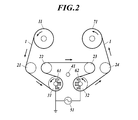
- Sectional drawing which shows an example of a structure of the organic electroluminescent element which concerns on this invention Schematic which shows an example of the manufacturing process of the gas barrier film which equipped with the discharge plasma CVD apparatus which has an opposing film-forming roller provided with the magnetic field generator applicable to formation of the gas barrier layer based on this invention.
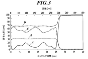
- the graph which shows an example of the silicon distribution curve of the gas barrier layer which concerns on this invention, an oxygen distribution curve, and a carbon distribution curve
- the method for producing an organic electroluminescence device of the present invention comprises a gas barrier layer containing a carbon atom, a silicon atom and an oxygen atom, an anode and a cathode, and at least between the anode and the cathode on a transparent resin film substrate.
- the silicon distribution curve, the oxygen distribution curve, and the carbon distribution curve showing the relationship between the ratio of the amount of silicon atoms, the ratio of the amount of oxygen atoms, and the ratio of the amount of carbon atoms are the above conditions (1) to (3 )
- the organic layer is formed by batch heat treatment within the range of the heat treatment temperature defined by the formula (a), that is, among the solvents contained in the coating liquid used for forming each organic layer,
- the organic layer is subjected to a batch heat treatment within the temperature range that is the upper limit of the heat treatment temperature at a temperature of the boiling point of the solvent having a high boiling point of ⁇ 10 ° C. or higher and the Tg of the transparent resin film substrate being used + 20 ° C. or lower.
- the upper limit of the heat treatment temperature is the transparent used, through the formation of all organic layers of the hole injection layer, the hole transport layer, the light emitting layer, and the electron transport layer. It is less than Tg + 20 degreeC of a resin film base material.
- the step of batch-heating the organic layer within the range of the heat treatment temperature defined by the formula (a) forms the final organic layer. It is preferable from the viewpoint of obtaining a more excellent light emission quantum efficiency (light emission luminance) and light emission lifetime after being performed and before forming the cathode.
- the organic layer unit is preferably composed of at least a hole injection layer, a hole transport layer, a light emitting layer, and an electron transport layer.
- the light emitting layer contains a light emitting host compound having a molecular weight of 2000 or less and a light emitting dopant having a molecular weight of 2000 or less from the viewpoint of obtaining superior light emission quantum efficiency (light emission luminance) and light emission lifetime.
- the gas barrier layer is disposed at opposing positions using a source gas containing an organosilicon compound and an oxygen gas, and a discharge plasma chemical vapor forming a discharge space between film forming rollers having a magnetic field therein. It is preferable to use a phase growth apparatus from the viewpoint that the composition is precisely controlled and a gas barrier layer having a desired element profile in the layer thickness direction can be stably formed.
- the transparent resin film substrate it is preferable to use a biaxially stretched polyethylene terephthalate film or polyethylene naphthalate film from the viewpoint of excellent economic efficiency and flexibility.
- the “gas barrier property” referred to in the present invention is a water vapor permeability (temperature: 60 ⁇ 0.5 ° C., relative humidity (RH): 90 ⁇ 2%) measured by a method according to JIS K 7129-1992. ) Is 3 ⁇ 10 ⁇ 3 g / m 2 ⁇ 24 h or less, and the oxygen permeability measured by a method according to JIS K 7126-1987 is 1 ⁇ 10 ⁇ 3 ml / m 2 ⁇ 24 h ⁇ atm or less. Means that.
- transparent means that the total light transmittance in the visible light wavelength region measured by a method in accordance with JIS K 7361-1: 1997 (test method for total light transmittance of resin transparent material) is 70. % Or more.
- the glass transition temperature Tg of a transparent resin film base material can be measured using the differential scanning calorimeter DSC220 by Seiko Electronic Industry Co., Ltd. according to JISK7121.
- the method for producing the organic electroluminescence element of the present invention is as follows. 1) forming a gas barrier layer containing carbon atoms, silicon atoms and oxygen atoms on a transparent resin film substrate; 2) forming a plurality of organic layers including at least a light emitting layer between the anode and the cathode and the anode and the cathode on the gas barrier layer; have.
- the gas barrier layer according to the present invention is based on the element distribution measurement in the depth direction by X-ray photoelectron spectroscopy, the distance from the surface in the layer thickness direction of the gas barrier layer, and the total of silicon atoms, oxygen atoms and carbon atoms
- the ratio of the amount of silicon atoms to the amount (100 at%) (referred to as “silicon atom ratio (at%)”), the ratio of the amount of oxygen atoms (referred to as “oxygen atomic ratio (at%)”), and the number of carbon atoms
- a silicon distribution curve, an oxygen distribution curve, and a carbon distribution curve showing a relationship with a ratio of amounts (referred to as “carbon atom ratio (at%)”) are formed in a configuration satisfying the following conditions (1) to (3). It is characterized by that.
- the composition of each atom continuously changes in the layer thickness direction, and the carbon distribution curve has an extreme value.
- the difference between the maximum extreme value and the minimum extreme value of the carbon atom ratio is 5 at% or more.
- a method for forming a gas barrier layer having the above-defined configuration for example, the method described in JP 2012-84306 A or International Publication No. 2012/046767 can be referred to. .
- the organic layer unit forms the cathode after forming the organic layer containing the solvent by applying each organic layer coating solution prepared by dissolving each organic layer forming material in the solvent.
- each organic layer is formed by batch heating the organic layer within the range of the heat treatment temperature defined by the following formula (a), Or, each time the organic layer unit is formed within the range of the heat treatment temperature defined by the following formula (b), each organic layer is formed by sequential heat treatment, It is characterized by.
- Structure of organic electroluminescence element >> In FIG. 1, an example of a structure of the organic electroluminescent element which concerns on this invention is shown.
- an organic EL element includes a transparent resin film substrate 1 and a gas barrier layer according to the present invention having a specific element profile in the layer thickness direction on one surface of the transparent resin film substrate 1. 2 is formed to constitute the gas barrier film F.
- the first electrode 3 is provided as an anode.
- the organic layer unit 4 comprised from a positive hole injection layer, a positive hole transport layer, a light emitting layer, and an electron carrying layer, for example, on the organic layer unit 4, for example, a cathode
- the second electrode 5 is arranged.
- the sealing member 6 is disposed in a state of covering the second electrode 5, and the organic EL element (EL) is sealed by the sealing member 6.
- an organic layer composed of, for example, a hole injection layer, a hole transport layer, a light emitting layer, and an electron transport layer by the first electrode 3 and the second electrode 5 facing each other.
- the unit 4 is sandwiched.
- the organic EL element (EL) is shown as a so-called bottom emission type configuration example in which light from the organic layer unit 4 is extracted from the transparent resin film substrate 1 side.
- Examples of the resin material constituting the transparent resin film substrate 1 include polyethylene terephthalate (abbreviation: PET), polyethylene naphthalate (abbreviation: abbreviation: PEN), polyester resins such as modified polyester, polyethylene (abbreviation: PE), polypropylene (abbreviation: PP), polyolefins such as polystyrene and cyclic olefin resin, vinyl resins such as polyvinyl chloride and polyvinylidene chloride, poly Ether ether ketone (abbreviation: PEEK), polysulfone (abbreviation: PSF), polyethersulfone (abbreviation: PES), polycarbonate (abbreviation: PC), polyamide, polyimide, acrylic resin, triacetyl cellulose (abbreviation: TAC), etc. Can be mentioned.
- PET polyethylene terephthalate
- PEN polyethylene naphthalate
- PEN polyester resins
- PE polyethylene
- PP
- biaxially stretched polyethylene terephthalate PET
- biaxially stretched polyethylene naphthalate PEN
- polyethersulfone PET
- PC polycarbonate
- PET biaxially stretched polyethylene terephthalate
- PEN biaxially stretched polyethylene naphthalate
- the film thickness of the transparent resin film substrate according to the present invention is preferably in the range of 1 to 1000 ⁇ m, and more preferably in the range of 10 to 100 ⁇ m.
- the transparent base material can be subjected to a surface treatment or an easy-adhesion layer.
- Conventionally known techniques can be applied to the surface treatment and the easy adhesion layer.
- the surface treatment include surface activation treatment such as corona discharge treatment, flame treatment, ultraviolet treatment, high frequency treatment, glow discharge treatment, active plasma treatment, and laser treatment.
- the easy adhesion layer examples include resins such as polyester, polyamide, polyurethane, vinyl copolymer, butadiene copolymer, acrylic copolymer, vinylidene copolymer, and epoxy copolymer. Ingredients can be mentioned.
- the easy adhesion layer may be a single layer, but may be composed of two or more layers in order to improve adhesion.
- the gas barrier layer according to the present invention is formed on at least one surface side of the transparent resin film substrate.
- the gas barrier layer according to the present invention is based on the element distribution measurement in the depth direction by X-ray photoelectron spectroscopy, the distance from the surface in the layer thickness direction of the gas barrier layer, and the total of silicon atoms, oxygen atoms and carbon atoms.
- the ratio of the amount of silicon atoms to the amount (100 at%) (referred to as “silicon atom ratio (at%)”), the ratio of the amount of oxygen atoms (referred to as “oxygen atomic ratio (at%)”), and the number of carbon atoms
- the silicon distribution curve, oxygen distribution curve and carbon distribution curve showing the relationship with the quantity ratio (referred to as “carbon atom ratio (at%)”) satisfy the following conditions (1) to (3): .
- composition of the gas barrier layer continuously changes in the layer thickness direction, and the carbon distribution curve has at least one extreme value.
- the difference between the maximum extreme value and the minimum extreme value of the carbon atom ratio is 5 at% or more.
- the present invention includes silicon, oxygen and carbon, and has at least one gas barrier layer satisfying all of the conditions (1) to (3) defined as the silicon distribution curve, oxygen distribution curve and carbon distribution curve. Just do it.
- the resin film substrate may have another constituent layer that does not satisfy at least one of the above conditions (1) to (3) as long as the object and effects of the present invention are not impaired.
- the gas barrier layer according to the present invention may further contain nitrogen or aluminum as a constituent element in addition to silicon, oxygen and carbon.
- the heating is performed under the temperature condition of the glass transition temperature of the resin film substrate + 20 ° C. or more.
- a crack also referred to as a crack
- the gas barrier layer according to the present invention that satisfies all of the above conditions (1) to (3) defined in the present invention is a resin film substrate as long as the heat treatment temperature is less than the glass transition temperature of the resin film substrate + 20 ° C. Even when some expansion and contraction of the gas occurs, the stress applied to the gas barrier layer can be efficiently relaxed, and as a result, it does not cause cracks, etc., and has good storage stability, and an organic layer coating formed thereon In this case, the temperature range that can be applied in the solvent removal step can be expanded.
- the region satisfying the formula (A) or the formula (B) defined in the present invention is 90% or more of the total thickness of the gas barrier layer, Preferably it is 95% or more, Most preferably, it is 100%.
- the gas barrier layer according to the present invention is characterized in that the carbon distribution curve has at least one extreme value in the above condition (1). Furthermore, in the gas barrier layer according to the present invention, the carbon distribution curve preferably has two or more extreme values, and particularly preferably has three or more extreme values. In the case of having at least three extreme values, the distance in the layer thickness direction between adjacent extreme values of the carbon distribution curve is preferably 200 nm or less, and more preferably 100 nm or less.
- the extreme value as used in the field of this invention is the maximum value (convex pattern) or the minimum value (concave pattern) of the atomic ratio (at%) of the element with respect to the distance from a surface layer surface in the layer thickness direction of a gas barrier layer.
- the maximum value as used in the present invention is a point where the atomic ratio value (at%) of an element changes from increase to decrease when the distance from the surface of the gas barrier layer is changed, and the element at that point
- the value of the atomic ratio of the element at a position where the distance from the surface of the gas barrier layer in the layer thickness direction of the gas barrier layer from the point is further changed by 20 nm is reduced by 3 at% or more than the atomic ratio value (at%). It means a point.
- the minimum value in the present invention is a point where the atomic ratio value (at%) of an element changes from decrease to increase when the distance from the surface of the gas barrier layer is changed, and the element at that point
- the atomic ratio value of the element at a position where the distance from the surface of the gas barrier layer in the thickness direction of the gas barrier layer in the thickness direction of the gas barrier layer is further changed by 20 nm from the point is increased by 3 at% or more. The point to do.
- the difference between the maximum extreme value and the minimum extreme value of the carbon atom ratio in the carbon distribution curve is 5 at% or more. It is characterized by.
- the difference between the maximum extreme value and the minimum extreme value of the atomic ratio of carbon is preferably 6 at% or more, particularly 7 at% or more. preferable.
- the oxygen distribution curve of the gas barrier layer preferably has at least one extreme value, more preferably has at least two extreme values, and has at least three extreme values. Is particularly preferred.
- the oxygen distribution curve has an extreme value, the dark spot resistance in the storage stability evaluation described later tends to be improved.
- the gas barrier in the thickness direction of the gas barrier layer at one extreme value and the other extreme value adjacent to the extreme value of the oxygen distribution curve.
- the absolute value of the difference in distance from the surface of the layer is preferably 200 nm or less, and more preferably 100 nm or less.
- the difference between the maximum extreme value and the minimum extreme value of the atomic ratio (at%) of oxygen in the oxygen distribution curve of the gas barrier layer may be 5 at% or more. Preferably, it is 6 at% or more, more preferably 7 at% or more. When the difference between the maximum value and the minimum value is 5 at% or more, the dark spot resistance in the storage stability evaluation described later tends to be improved.
- the difference between the maximum extreme value and the minimum extreme value of the atomic ratio of silicon is preferably less than 5 at%, more preferably less than 4 at%. Preferably, it is particularly preferably less than 3 at%. If the difference between the maximum extreme value and the minimum extreme value is less than 5 at%, the dark spot resistance in the storage stability evaluation described later tends to be improved.
- the maximum extreme value and the minimum extreme value of the sum (at%) of the atomic ratio of oxygen and carbon in the oxygen-carbon distribution curve The difference in value is preferably less than 5 at%, more preferably less than 4 at%, and particularly preferably less than 3 at%. If the difference between the maximum extreme value and the minimum extreme value is less than 5 at%, the dark spot resistance in the storage stability evaluation described later tends to be improved.
- the silicon distribution curve, oxygen distribution curve, carbon distribution curve and oxygen-carbon distribution curve of the gas barrier layer according to the present invention are measured by X-ray photoelectron spectroscopy (XPS) and a rare gas such as argon.
- XPS X-ray photoelectron spectroscopy
- argon a rare gas such as argon.
- XPS depth profile measurement in which the surface composition analysis is sequentially performed while exposing the inside of the sample.
- the element distribution curve obtained by such XPS depth profile measurement can be created, for example, with the vertical axis as the atomic ratio (unit: at%) of each element and the horizontal axis as the etching time (sputtering time).
- the etching time generally correlates with the distance from the surface layer of the gas barrier layer in the layer thickness direction to the layer thickness direction.
- the “distance from the surface of the gas barrier layer in the thickness direction of the barrier layer” can be calculated from the relationship between the etching rate and the etching time employed in the XPS depth profile measurement.
- etching rate is 0.05 nm / It is preferable to set to sec (SiO 2 thermal oxide film conversion value).
- the gas barrier layer according to the present invention has a uniform gas barrier layer with excellent gas barrier properties with no variation in characteristics in the entire surface area, and the gas barrier layer is in the film surface direction. In the (direction parallel to the surface of the gas barrier layer), the composition is preferably substantially uniform (uniform).
- the number of extreme values of the carbon distribution curve obtained at any two measurement locations is the same, and the carbon atoms in the respective carbon distribution curves It means that the difference between the maximum extreme value and the minimum extreme value of the ratio is the same or within 5 at%.
- the carbon distribution curve changes substantially continuously in the layer thickness direction.
- the fact that the carbon distribution curve changes substantially continuously means that the carbon distribution curve does not include a portion where the atomic ratio of carbon changes discontinuously.
- a plurality of gas barrier layers may be provided.
- the constituent materials of the plurality of gas barrier layers may be the same or different.
- the gas barrier layer may be formed in two or more layers on one side of the transparent resin film substrate. Each may be formed on the surface side.
- the atomic ratio of silicon, the atomic ratio of oxygen and the atomic ratio of carbon satisfy the condition (3).
- the atomic ratio (at%) of the silicon atom content to the total amount of silicon atoms, oxygen atoms and carbon atoms in the gas barrier layer according to the present invention Is preferably in the range of 25 to 45 at%, and more preferably in the range of 30 to 40 at%.
- the atomic ratio (at%) of the oxygen atom content to the total amount of silicon atoms, oxygen atoms and carbon atoms in the gas barrier layer according to the present invention is preferably in the range of 33 to 67 at%. More preferably, it is within the range of 45 to 67 at%. Further, the atomic ratio (at%) of the carbon atom content to the total amount of silicon atoms, oxygen atoms and carbon atoms in the gas barrier layer according to the present invention is preferably in the range of 3 to 33 at%, More preferably, it is in the range of 3 to 25 at%.
- the atomic ratio of silicon, the atomic ratio of oxygen, and the atomic ratio of carbon are the conditions (3
- the atomic ratio of the content of silicon atoms to the total amount of silicon atoms, oxygen atoms and carbon atoms in the gas barrier layer according to the present invention (at %) Is preferably in the range of 25 to 45 at%, and more preferably in the range of 30 to 40 at%.
- the atomic ratio (at%) of the oxygen atom content to the total amount of silicon atoms, oxygen atoms and carbon atoms in the gas barrier layer according to the present invention is preferably in the range of 1 to 33 at%. More preferably, it is within the range of 10 to 27 at%. Further, the atomic ratio (at%) of the carbon atom content to the total amount of silicon atoms, oxygen atoms and carbon atoms in the gas barrier layer is preferably in the range of 33 to 66 at%, preferably 40 to 57 at%. % Is more preferable.
- the layer thickness of the gas barrier layer is preferably in the range of 5 to 3000 nm, more preferably in the range of 10 to 2000 nm, and particularly preferably in the range of 100 to 1000 nm.
- the method for forming the gas barrier layer according to the present invention is not particularly limited, but a layer formed by plasma chemical vapor deposition is preferable.
- a gas barrier layer formed by such a plasma chemical vapor deposition method a film substrate is disposed on the pair of film forming rollers, and plasma is generated by applying and discharging between the pair of film forming rollers. More preferably, the layer is formed by plasma chemical vapor deposition.
- the film forming gas used in such a plasma chemical vapor deposition method preferably contains an organosilicon compound and oxygen, and the content of oxygen in the film forming gas is the organic gas in the film forming gas. It is preferable that the amount is less than or equal to the theoretical oxygen amount necessary for complete oxidation of the entire amount of the silicon compound.
- the gas barrier layer is preferably a layer formed by a continuous film forming process.
- the plasma chemical vapor deposition method may be a Penning discharge plasma type chemical vapor deposition method.
- a method of generating plasma discharge in a space between a plurality of film forming rollers can be applied, but using a pair of film forming rollers, More preferably, a transparent resin film substrate is disposed on each of the pair of film forming rollers, and plasma is generated by discharging between the pair of film forming rollers. Furthermore, a method of forming by a discharge plasma chemical vapor deposition method using a source gas containing an organic silicon compound and an oxygen gas and having a discharge space between rollers having a magnetic field is preferable.
- Examples of a discharge plasma chemical vapor deposition apparatus having a discharge space between rollers having such a magnetic field are disclosed in, for example, JP 2008-196001 A, JP 2012-84306 A, or International Publication No. 2012/046767. Reference may be made to the apparatus described.
- a method of forming the gas barrier layer on the surface of a long roll-shaped transparent resin film substrate by a roll-to-roll method is preferable.
- An apparatus capable of forming a gas barrier layer by such a plasma chemical vapor deposition method is not particularly limited, and includes at least a pair of film forming rollers and a plasma power source, and the pair of film forming films. It is preferable that the apparatus has a configuration capable of discharging between the rollers. For example, when the manufacturing apparatus shown in FIG. 2 is used, a roll-to-roll method is performed while using plasma chemical vapor deposition. Can also be manufactured.
- FIG. 2 shows a gas barrier property provided with an inter-roller discharge plasma CVD apparatus having a pair of film-forming rollers provided at a position opposite to each other, which is applicable to the formation of a gas barrier layer according to the present invention. It is the schematic which shows an example of the manufacturing process of a film.
- the inter-roller discharge plasma CVD apparatus (hereinafter also referred to as plasma CVD apparatus) having a magnetic field shown in FIG. 2 mainly includes a delivery roller 11, transport rollers 21, 22, 23 and 24, a film formation roller 31 and 32, a film forming gas supply pipe 41, a plasma generation power source 51, magnetic field generators 61 and 62 installed inside the film forming rollers 31 and 32, and a winding roller 71.
- a plasma CVD manufacturing apparatus at least the film forming rollers 31 and 32, the film forming gas supply pipe 41, the plasma generating power source 51, and the magnetic field generating apparatuses 61 and 62 are not shown in a vacuum.
- a vacuum chamber (not shown) is connected to a vacuum pump (not shown), and the pressure in the vacuum chamber can be appropriately adjusted by this vacuum pump. Yes.
- each film forming roller generates plasma so that a pair of film forming rollers (the film forming roller 31 and the film forming roller 32) can function as a pair of counter electrodes. It is connected to the power source 51 for use.
- the power source 51 for use By supplying electric power to the pair of film forming rollers (the film forming roller 31 and the film forming roller 32) from the power source 51 for generating plasma, the space between the film forming roller 31 and the film forming roller 32 can be discharged.
- plasma can be generated in a space (also referred to as a discharge space) between the film formation roller 31 and the film formation roller 32.
- the film-forming roller 31 and the film-forming roller 32 are used as electrodes in this way, materials and designs that can be used as electrodes may be changed as appropriate.
- the pair of film forming rollers (film forming rollers 31 and 32) be arranged so that their central axes are substantially parallel on the same plane.
- the film forming roller 31 and the film forming roller 32 are characterized by being provided with magnetic field generators 61 and 62 fixed so as not to rotate even if the film forming roller rotates.
- the film forming roller 31 and the film forming roller 32 known rollers can be appropriately used.
- the film forming rollers 31 and 32 those having the same diameter are preferably used from the viewpoint of forming a thin film (gas barrier layer) more efficiently.
- the diameters of the film forming rollers 31 and 32 are preferably in the range of 100 to 1000 mm ⁇ , particularly in the range of 100 to 700 mm ⁇ , from the viewpoint of discharge conditions, chamber space, and the like. If the diameter is 100 mm ⁇ or more, it is preferable that the plasma discharge space is not reduced, the productivity is not deteriorated, the total amount of heat of the plasma discharge can be prevented from being applied to the film in a short time, and the residual stress is hardly increased.
- a diameter of 1000 mm ⁇ or less is preferable because practicality can be maintained in terms of device design including uniformity of the plasma discharge space.
- the winding roller 71 is not particularly limited as long as it can wind the resin base material 1 on which the gas barrier layer is formed, and a known roller can be used as appropriate.
- the film forming gas supply pipe 41 one capable of supplying or discharging the source gas and the oxygen gas at a predetermined rate can be appropriately used.
- the plasma generating power source 51 a conventionally known power source for a plasma generating apparatus can be used.
- Such a power source 51 for generating plasma supplies power to the film forming roller 31 and the film forming roller 32 connected thereto, and makes it possible to use these as counter electrodes for discharge.
- a power source AC power source or the like
- a power source capable of alternately reversing the polarities of a pair of film forming rollers is used. It is preferable to use it.
- the applied power can be in the range of 100 W to 10 kW, and the AC frequency is 50 Hz. More preferably, it can be in the range of -500 kHz.
- the magnetic field generators 61 and 62 known magnetic field generators can be used as appropriate.
- the gas barrier layer according to the present invention can be formed by appropriately adjusting the diameter of the roller and the conveying speed of the resin base material. That is, using the plasma CVD apparatus shown in FIG. 2, a magnetic field is generated between a pair of film forming rollers (film forming rollers 31 and 32) while supplying a film forming gas (raw material gas, etc.) into the vacuum chamber.
- the film forming gas (raw material gas or the like) is decomposed by plasma, and on the surface of the resin base material 1 on the film forming roller 31 and on the surface of the resin base material 1 on the film forming roller 32.
- the gas barrier layer according to the present invention is formed by the plasma CVD method. In such film formation, the resin base material 1 is conveyed by the delivery roller 11 and the film formation roller 31, respectively, so that the resin base material 1 is formed by a roll-to-roll continuous film formation process.
- the gas barrier layer is formed on the surface.
- the source gas constituting the film forming gas used for forming the gas barrier layer according to the present invention can be appropriately selected according to the material of the gas barrier layer to be formed, and at least an organosilicon compound containing silicon is used. Is preferred.
- organosilicon compound applicable to the present invention examples include hexamethyldisiloxane, 1,1,3,3-tetramethyldisiloxane, vinyltrimethylsilane, methyltrimethylsilane, hexamethyldisilane, methylsilane, dimethylsilane, and trimethyl.
- examples thereof include silane, diethylsilane, propylsilane, phenylsilane, vinyltriethoxysilane, vinyltrimethoxysilane, tetramethoxysilane, tetraethoxysilane, phenyltrimethoxysilane, methyltriethoxysilane, and octamethylcyclotetrasiloxane.
- organosilicon compounds hexamethyldisiloxane and 1,1,3,3-tetramethyldisiloxane are preferable from the viewpoints of handling in film formation and gas barrier properties of the obtained gas barrier layer. Moreover, these organosilicon compounds can be used individually by 1 type or in combination of 2 or more types.
- a reactive gas may be used as the film forming gas.
- a gas that reacts with the raw material gas to become an inorganic compound such as an oxide or a nitride can be appropriately selected and used.
- a reaction gas for forming an oxide for example, oxygen or ozone can be used.
- a reactive gas for forming nitride nitrogen and ammonia can be used, for example.
- These reaction gases can be used alone or in combination of two or more. For example, when forming an oxynitride, a reaction gas for forming an oxide and a nitride are formed. The reaction gas can be used in combination.
- a carrier gas may be used as necessary.
- a discharge gas may be used as necessary in order to generate plasma discharge.
- carrier gas and discharge gas known ones can be used as appropriate, and for example, rare gases such as helium, argon, neon, xenon, hydrogen gas, and nitrogen gas can be used.
- the ratio of the source gas and the reactive gas is the amount of the reactive gas that is theoretically necessary to completely react the raw material gas and the reactive gas. It is preferable not to make the ratio of the reaction gas excessively higher than the ratio of. If the ratio of the reaction gas is excessive, a thin film that satisfies all of the above conditions (1) to (3) cannot be obtained.
- the deposition gas contains an organosilicon compound and oxygen, the amount of oxygen should be less than or equal to the theoretical oxygen amount necessary for complete oxidation of the entire amount of the organosilicon compound in the deposition gas. preferable.
- hexamethyldisiloxane an organosilicon compound, also referred to as HMDSO, (CH 3 ) 6 Si 2 O) as a source gas and oxygen (O 2 ) as a reaction gas will be described.
- a film-forming gas containing hexamethyldisiloxane ((CH 3 ) 6 Si 2 O) as a source gas and oxygen (O 2 ) as a reaction gas is reacted by a plasma CVD method to form a silicon-oxygen system (
- a reaction represented by the following reaction formula (1) occurs by the film forming gas, and a thin film made of silicon dioxide SiO 2 is formed.
- Reaction formula (1) (CH 3 ) 6 Si 2 O + 12O 2 ⁇ 6CO 2 + 9H 2 O + 2SiO 2
- the amount of oxygen required to completely oxidize 1 mol of hexamethyldisiloxane is 12 mol. Therefore, when the film forming gas contains 12 moles or more of oxygen with respect to 1 mole of hexamethyldisiloxane and is completely reacted, a uniform silicon dioxide film is formed.
- the ratio is controlled to a flow rate equal to or less than the raw material ratio of the complete reaction, which is the theoretical ratio, and the incomplete reaction is performed. That is, it is necessary to set the amount of oxygen to less than 12 moles of the stoichiometric ratio with respect to 1 mole of hexamethyldisiloxane.
- the raw material hexamethyldisiloxane and the reaction gas, oxygen are supplied from the gas supply unit to the film formation region to form a film. Even if the molar amount (flow rate) is 12 times the molar amount (flow rate) of the starting hexamethyldisiloxane, the reaction cannot actually proceed completely, and oxygen content It is considered that the reaction is completed only when the amount is supplied in a large excess with respect to the stoichiometric ratio.
- the molar amount (flow rate) of oxygen may be 20 times or more the molar amount (flow rate) of hexamethyldisiloxane as a raw material. Therefore, the molar amount (flow rate) of oxygen with respect to the molar amount (flow rate) of hexamethyldisiloxane as a raw material is preferably 12 times or less, more preferably 10 times or less, which is the stoichiometric ratio. It is.
- the transparency of the gas barrier layer is lowered, and such a gas barrier film is flexible for electronic devices such as devices that require transparency such as organic EL devices and organic thin film solar cells. It can no longer be used for the substrate. Therefore, the lower limit of the molar amount (flow rate) of oxygen relative to the molar amount (flow rate) of hexamethyldisiloxane in the film forming gas should be greater than 0.1 times the molar amount (flow rate) of hexamethyldisiloxane. It is more preferable that the amount be more than 0.5 times.
- the pressure (degree of vacuum) in the vacuum chamber can be adjusted as appropriate according to the type of the raw material gas, but is preferably in the range of about 0.5 to 100 Pa.
- an electrode drum connected to a plasma generation power source 51 (in FIG. 2, an electrode drum connected to a plasma generation power source 51 (in FIG.
- the electric power applied to the film rollers 31 and 32) can be adjusted as appropriate according to the type of source gas, the pressure in the vacuum chamber, etc., and cannot be specified in general. However, it is preferably within a range of about 0.1 to 10 kW. If the applied power is in such a range, no generation of particles (illegal particles) is observed, and the amount of heat generated during film formation is within the control range. It is also possible to prevent thermal deformation of the base material, performance deterioration due to heat, and generation of wrinkles during film formation. In addition, it is possible to prevent damage to the film forming roller due to melting of the resin base material by heat and generation of a large current discharge between the bare film forming rollers.
- the conveyance speed (line speed) of the resin base material 1 can be appropriately adjusted according to the type of raw material gas, the pressure in the vacuum chamber, etc., but is preferably in the range of 0.25 to 100 m / min. More preferably, it is within the range of 0.5 to 20 m / min. If the line speed is within the above range, wrinkles due to the heat of the resin base material hardly occur, and the thickness of the formed gas barrier layer can be sufficiently controlled.
- Anode / hole injection layer / hole transport layer / light emitting layer / electron injection layer / cathode (ii) Anode / hole injection layer / hole transport layer / light emitting layer / electron transport layer / electron injection layer / cathode [Organic layer] Although it does not specifically limit as an organic layer which comprises the organic layer unit in this invention, For example, a hole injection layer, a positive hole transport layer, a light emitting layer, an electron carrying layer, and an electron which were illustrated to said (ii), for example An injection layer etc. can be mentioned.
- a plurality of organic layers including a hole injection layer, a hole transport layer, a light emitting layer, and an electron transport layer are prepared by dissolving each organic layer forming material (organic material) in a solvent. It is formed by applying sequentially using a forming coating solution.
- the target organic material can be dissolved, and at least less than Tg + 30 ° C. of the transparent resin film substrate used for preparing the organic EL element.
- a solvent having a boiling point is selected.
- the type of solvent applicable to the present invention varies depending on the type of resin film substrate to be applied.
- methanol (boiling point: 64.7 ° C), ethanol (boiling point: 78.3 ° C), isopropyl alcohol (boiling point: 82.3 ° C), 1-propanol (boiling point: 97.2 ° C), alcohols such as n-butanol (boiling point: 117.7 ° C.), s-butanol (boiling point: 99.5 ° C.), t-butanol (boiling point: 82.5 ° C.), acetone (boiling point: 56.1 ° C.), Ketones such as methyl ethyl ketone (boiling point: 79.6 ° C), cyclohexanone (boiling point: 155.7 ° C), ethyl acetate (boiling point: 77.1 ° C), n-butyl acetate (boiling point: 126.1 ° C),
- the boiling point of the solvent according to the present invention is a value measured at atmospheric pressure, and is described in detail in, for example, “Newly published Solvent Pocketbook” (edited by the Society for Synthetic Organic Chemistry, published by Ohmsha, published in 1994, 1st edition). Data are listed and can be used as a reference.
- a dispersion device or the like when preparing each organic layer coating liquid, a dispersion device or the like can be used, and as an applicable dispersion method, a dispersion method such as ultrasonic dispersion, high shear force dispersion or media dispersion can be applied. it can.
- the organic layer forming material according to the present invention varies depending on the type of the organic layer, a specific forming material will be described in the detailed description of the layer configuration of the organic EL below.
- the coating liquid for organic layer formation and the organic layer formation material change the name according to the name of the organic layer.
- the organic layer forming coating liquid and the organic layer forming material in the light emitting layer are referred to as the light emitting layer forming coating liquid and the light emitting layer forming material.
- the light emitting layer according to the present invention is a layer that emits light by recombination of electrons and holes injected from the electrode, the electron transport layer, or the hole transport layer, and the light emitting region is within the layer of the light emitting layer. Or the interface area
- the layer thickness of the light emitting layer is not particularly limited, but from the viewpoint of improving the uniformity of the light emitting layer to be formed and preventing application of unnecessary high voltage at the time of light emission, and improving the stability of the emission color against the driving current. It is preferable to adjust within the range of 2 to 200 nm, and more preferably within the range of 5 to 100 nm.
- a metal complex compound can be used as the light emitting layer forming material according to the present invention.
- a host compound can be used together with a metal complex compound.
- the molecular weight of the light emitting layer forming material is not particularly limited, but is preferably 2000 or less.
- Fluorescent dopants or phosphorescent dopants can be used as the metal complex compound according to the present invention.
- the metal complex compound used in the light emitting layer of the organic EL device according to the present invention preferably contains a phosphorescent dopant.
- a phosphorescent dopant is a compound in which light emission from an excited triplet is observed. Specifically, it is a compound that emits phosphorescence at room temperature (25 ° C.). It is defined as a compound of 01 or more, and a preferable phosphorescence quantum yield is 0.1 or more.
- the phosphorescent quantum yield can be measured by the method described in Spectroscopic II, page 398 (1992 edition, Maruzen) of the Fourth Edition Experimental Chemistry Course 7. Although the phosphorescence quantum yield in a solution can be measured using various solvents, the phosphorescence dopant applied in the present invention is the above phosphorescence quantum yield (0.01 or more) in any solvent. Should be achieved.
- the following two types of light emission principles using phosphorescent dopants can be mentioned.
- One is the recombination of carriers on the light-emitting host where carriers are transported, and the excited state of the light-emitting host is generated.
- It is an energy transfer type in which light emission from the phosphorescent dopant is obtained by transferring to the dopant.
- the phosphorescent dopant becomes a carrier trap, and carrier recombination occurs on the phosphorescent dopant, and light emission from the phosphorescent dopant.
- the excited state energy of the phosphorescent dopant is required to be lower than the excited state energy of the light emitting host.
- the phosphorescent dopant can be appropriately selected from known materials conventionally used for the light emitting layer of the organic EL device. Specific examples of typical compounds used as phosphorescent dopants are shown below, but the present invention is not limited thereto. These compounds are described, for example, in Inorg. Chem. 40, 1704 to 1711, and the like.
- iridium complex having a structure represented by the following general formula (1) it is particularly preferable to use an iridium complex having a structure represented by the following general formula (1) as the metal complex having a blue emission wavelength.
- Z represents a hydrocarbon ring group or a heterocyclic group.
- P 1 -L1-P 2 represents a bidentate ligand, and P 1 and P 2 each independently represent a carbon atom, a nitrogen atom, or an oxygen atom.
- L1 represents an atomic group forming a ligand bidentate with P 1 and P 2.
- R 81 to R 86 each represent a hydrogen atom or a substituent.
- j1 represents an integer of 1 to 3
- j2 represents an integer of 0 to 2
- j1 + j2 is 2 or 3.
- M 1 represents a group 8-10 transition metal element in the periodic table.
- examples of the bidentate ligand represented by P 1 -L1-P 2 include substituted or unsubstituted phenylpyridine, phenylpyrazole, phenylimidazole, phenyltriazole, phenyltetrazole, Examples include pyraza ball, acetylacetone, and picolinic acid.
- Examples of the hydrocarbon ring group represented by Z include a non-aromatic hydrocarbon ring group and an aromatic hydrocarbon ring group.
- Examples of the non-aromatic hydrocarbon ring group include a cyclopropyl group, a cyclopentyl group, and a cyclohexyl group. And may be substituted or unsubstituted.
- aromatic hydrocarbon ring group examples include, for example, phenyl group, p-chlorophenyl group, mesityl group, tolyl group, xylyl group, naphthyl group, anthryl group, azulenyl. Group, acenaphthenyl group, fluorenyl group, phenanthryl group, indenyl group, pyrenyl group, biphenylyl group and the like. These groups may be substituted or unsubstituted.
- Examples of the heterocyclic group represented by Z include a non-aromatic heterocyclic group and an aromatic heterocyclic group.
- Examples of the non-aromatic heterocyclic group include an epoxy ring, an aziridine ring, a thiirane ring, Oxetane ring, azetidine ring, thietane ring, tetrahydrofuran ring, dioxolane ring, pyrrolidine ring, pyrazolidine ring, imidazolidine ring, oxazolidine ring, tetrahydrothiophene ring, sulfolane ring, thiazolidine ring, ⁇ -caprolactone ring, ⁇ -caprolactam ring, piperidine ring , Hexahydropyridazine ring, hexahydropyrimidine ring, piperazine ring, morpholine ring, tetrahydropyran ring, 1,3-d
- R 81 to R 86 each represent a hydrogen atom or a substituent.
- substituents include an alkyl group (for example, a methyl group, Ethyl group, propyl group, isopropyl group, t-butyl group, pentyl group, hexyl group, octyl group, dodecyl group, tridecyl group, tetradecyl group, pentadecyl group, etc.), cycloalkyl group (for example, cyclopentyl group, cyclohexyl group, etc.)
- An alkenyl group eg, vinyl group, allyl group, etc.
- an alkynyl group eg, ethynyl group, propargyl group, etc.
- aromatic hydrocarbon ring group aromatic hydrocarbon ring group (aromatic carbocyclic group, aryl group, etc., for example, a phenyl
- aromatic hydrocarbon ring groups also called aromatic carbocyclic groups, aryl groups, etc., for example, phenyl group, p-chlorophenyl group, mesityl group, tolyl group, xylyl group, naphthyl group, anthryl group, azulenyl group, acenaphthenyl group, etc.
- the light emitting layer when the light emitting layer contains a metal complex compound, the light emitting layer may contain one kind of metal complex compound or two or more kinds of metal complex compounds having different emission maximum wavelengths. .
- the light emitting layer preferably contains a light emitting dopant having a molecular weight of 2000 or less.
- a compound having a phosphorescence quantum yield of phosphorescence emission at room temperature (25 ° C.) of less than 0.1 is preferable. More preferably, the phosphorescence quantum yield is less than 0.01. Moreover, it is preferable that the volume ratio in the layer is 50% or more among the compounds contained in a light emitting layer.
- known host compounds may be used alone or in combination of two or more. By using a plurality of types of host compounds, it is possible to adjust the movement of charges, and the organic EL element can be made highly efficient.
- the host compound used in the present invention may be a conventionally known low molecular compound or a high molecular compound having a repeating unit, and a low molecular compound having a polymerizable group such as a vinyl group or an epoxy group (evaporation polymerizable light emitting host).
- a light emitting host compound having a molecular weight of 2000 or less for the light emitting layer.
- the known host compound a compound that has a hole transporting ability and an electron transporting ability, prevents the emission of light from being increased in wavelength, and has a high Tg (glass transition temperature) is preferable.
- the glass transition point (Tg) is a value determined by a method based on JIS-K-7121 using DSC (Differential Scanning Colorimetry).
- the host compound used in the present invention is preferably a carbazole derivative, more preferably a dibenzofuran compound which is a carbazole derivative.
- the injection layer can be provided as necessary.
- the injection layer there are an electron injection layer and a hole injection layer.
- the injection layer may exist between the anode and the light emitting layer or the hole transport layer and between the cathode and the light emitting layer or the electron transport layer.
- the injection layer referred to in the present invention is a layer provided between the electrode and the organic layer in order to lower the driving voltage and improve the light emission luminance.
- the organic EL element and its forefront of industrialization June 30, 1998, NTS
- the details are described in Volume 2, Chapter 2, “Electrode Materials” (pages 123 to 166) of “Part 2”.
- hole injection layer Details of the hole injection layer and its constituent materials are described, for example, in JP-A-9-45479, JP-A-9-260062, and JP-A-8-288069.
- Examples of the forming material applicable to the formation of the hole injection layer include triazole derivatives, oxadiazole derivatives, imidazole derivatives, pyrazoline derivatives and pyrazolone derivatives, phenylenediamine derivatives, arylamine derivatives, amino-substituted chalcone derivatives, oxazole derivatives, Examples include polymers containing styryl anthracene derivatives, fluorenone derivatives, hydrazone derivatives, stilbene derivatives, silazane derivatives, aniline copolymers, polyarylalkane derivatives, or conductive polymers, preferably polythiophene derivatives, polyaniline derivatives, polypyrrole derivatives. More preferably a polythiophene derivative.
- the forming material applicable to the formation of the electron injection layer examples include a metal compound. Specific examples include a metal buffer layer typified by strontium and aluminum, an alkali metal compound buffer layer typified by lithium fluoride, Examples thereof include an alkaline earth metal compound buffer layer typified by magnesium fluoride and an oxide buffer layer typified by aluminum oxide.
- the buffer layer (injection layer) is preferably a very thin layer, preferably potassium fluoride or sodium fluoride.
- the layer thickness is about 0.1 to 5 ⁇ m, preferably in the range of 0.1 to 100 nm, more preferably in the range of 0.5 to 10 nm, and most preferably in the range of 0.5 to 4 nm.
- Examples of the hole transport layer forming material that can be used for forming the hole transport layer according to the present invention include the same compounds that can be applied in the hole injection layer.
- a porphyrin compound, an aromatic tertiary amine compound, and a styrylamine compound can be mentioned. Among them, it is particularly preferable to use an aromatic tertiary amine compound.
- aromatic tertiary amine compounds and styrylamine compounds include N, N, N ′, N′-tetraphenyl-4,4′-diaminophenyl; N, N′-diphenyl-N, N′— Bis (3-methylphenyl)-[1,1′-biphenyl] -4,4′-diamine (abbreviation: TPD); 2,2-bis (4-di-p-tolylaminophenyl) propane; -Bis (4-di-p-tolylaminophenyl) cyclohexane; N, N, N ', N'-tetra-p-tolyl-4,4'-diaminobiphenyl; 1,1-bis (4-di-p -Tolylaminophenyl) -4-phenylcyclohexane; bis (4-dimethylamino-2-methylphenyl) phenylmethane; bis (4-di-p-tol
- polymer materials in which these materials are introduced into polymer chains or these materials are used as polymer main chains can also be used.
- inorganic compounds such as p-type-Si and p-type-SiC can also be used as the hole injection layer material and the hole transport layer material.
- JP-A-4-297076 JP-A-2000-196140, JP-A-2001-102175, J. Pat. Appl. Phys. , 95, 5773 (2004), JP-A-11-251067, J. MoI. Huang et. al. It is also possible to use a hole transport layer material having a so-called p-type semiconducting property as described in the literature (Applied Physics Letters 80 (2002), p. 139) and Japanese translations of PCT publication No. 2003-519432.
- the layer thickness of the hole transport layer is not particularly limited, but is usually about 5 nm to 5 ⁇ m, preferably 5 to 200 nm.
- the hole transport layer may have a single layer structure composed of one or more of the above materials.
- the electron transport layer as used in the present invention contains a material having a function of transporting electrons, and in a broad sense, an electron injection layer and a hole blocking layer are also included in the electron transport layer.
- the electron transport layer can be provided as a single layer or a plurality of layers.
- an electron transport layer material (a hole blocking layer material used for an electron transport layer provided adjacent to the light emitting layer on the cathode side) is used. As long as it has a function of transmitting electrons injected from the cathode to the light-emitting layer.
- an electron transport layer material any one of conventionally known compounds may be selected and used. Examples thereof include metal complexes such as a fluorene derivative, a carbazole derivative, an azacarbazole derivative, an oxadiazole derivative, a trizole derivative, a cylola derivative, a pyridine derivative, a pyrimidine derivative, and an 8-quinolinol derivative.
- metal-free or metal phthalocyanine or those having terminal ends substituted with an alkyl group or a sulfonic acid group can be preferably used as the electron transport layer material.
- carbazole derivatives Among these, carbazole derivatives, azacarbazole derivatives, pyridine derivatives and the like are preferable in the present invention, and dibenzofuran compounds which are carbazole derivatives are more preferable.
- the layer thickness of the electron transport layer is not particularly limited, but is usually about 5 nm to 5 ⁇ m, preferably 5 to 200 nm.
- the electron transport layer may have a single layer structure composed of one or more of the above materials.
- a material doped with impurities as a guest material can be used for an electron transport layer having high n property.
- Examples thereof include JP-A-4-297076, JP-A-10-270172, JP-A-2000-196140, 2001-102175, J.A. Appl. Phys. 95, 5773 (2004), and the like.
- an alkali metal salt of an organic substance it is preferable to apply an alkali metal salt of an organic substance to the electron transport layer.
- organic substance there are no particular restrictions on the type of organic substance, but formate, acetate, propionic acid, butyrate, valerate, caproate, enanthate, caprylate, oxalate, malonate, succinic acid Salt, benzoate, phthalate, isophthalate, terephthalate, salicylate, pyruvate, lactate, malate, adipate, mesylate, tosylate, benzenesulfonate
- the kind of alkali metal of the organic alkali metal salt is not particularly limited, and examples thereof include Na, K, and Cs, preferably K, Cs, and more preferably Cs.
- the alkali metal salt of the organic substance include a combination of the organic substance and the alkali metal, preferably, formic acid Li, formic acid K, Na formic acid, formic acid Cs, Li acetate, K acetate, Na acetate, Cs acetate, Lipropionate, Propionic acid Na, propionic acid K, propionic acid Cs, oxalic acid Li, oxalic acid Na, oxalic acid K, oxalic acid Cs, malonic acid Li, malonic acid Na, malonic acid K, malonic acid Cs, succinic acid Li, succinic acid Na, succinic acid K, succinic acid Cs, benzoic acid Li, benzoic acid Na, benzoic acid K, benzoic acid Cs, more preferably Li acetate,
- the content of these doping materials is preferably in the range of 1.5 to 35% by mass, more preferably in the range of 3 to 25% by mass, and most preferably in the range of 5 to 5% with respect to the electron transport layer to be added. It is in the range of 15% by mass.
- an anode using a metal, an alloy, an electrically conductive compound and a mixture thereof having a high work function (4 eV or more) is preferably used.
- an electrode material include metals such as Au, and conductive transparent materials such as CuI, indium tin oxide (abbreviation: ITO), SnO 2 , and ZnO.
- conductive transparent materials such as CuI, indium tin oxide (abbreviation: ITO), SnO 2 , and ZnO.
- an amorphous material such as IDIXO (In 2 O 3 —ZnO) capable of forming a transparent conductive film may be used.
- these electrode materials may be formed into a thin film by a method such as vapor deposition or sputtering, and a desired pattern may be formed by photolithography, or when the pattern accuracy is not so required, for example, the required accuracy is 100 ⁇ m. If it is about the above, a pattern may be formed through a mask having a desired shape at the time of vapor deposition or sputtering of the electrode material. Or when using the substance which can be apply
- the transmittance of the anode is desirably 10% or more, and the sheet resistance as the anode is preferably several hundred ⁇ / ⁇ or less. Further, although depending on the material, the film thickness is usually in the range of 10 to 1000 nm, preferably in the range of 10 to 200 nm.
- cathode a material having a work function (4 eV or less) metal (hereinafter referred to as an electron injecting metal), an alloy, an electrically conductive compound, and a mixture thereof as an electrode material is used.
- electrode materials include sodium, sodium-potassium alloy, magnesium, lithium, magnesium / copper mixture, magnesium / silver mixture, magnesium / aluminum mixture, magnesium / indium mixture, aluminum / aluminum oxide (Al 2 O 3 ) Mixtures, indium, lithium / aluminum mixtures, rare earth metals and the like.
- a mixture of an electron injecting metal and a second metal which is a stable metal having a larger work function than this for example, a magnesium / silver mixture, Magnesium / aluminum mixtures, magnesium / indium mixtures, aluminum / aluminum oxide (Al 2 O 3 ) mixtures, lithium / aluminum mixtures, aluminum and the like are preferred.
- the cathode can be produced by forming a thin film of these electrode materials by a method such as vapor deposition or sputtering.
- the sheet resistance as the cathode is preferably several hundred ⁇ / ⁇ or less, and the film thickness is usually selected in the range of 10 nm to 5 ⁇ m, preferably in the range of 50 to 200 nm.
- the film thickness is usually selected in the range of 10 nm to 5 ⁇ m, preferably in the range of 50 to 200 nm.
- a transparent or translucent cathode can be manufactured by forming the above metal as a cathode within a film thickness range of 1 to 20 nm and then forming the conductive transparent material mentioned in the description of the anode on the metal. By applying this, it is possible to produce an organic EL element in which both the anode and the cathode are transparent.
- an organic layer unit composed of a hole injection layer, a hole transport layer, a light emitting layer, and an electron transport layer is prepared by using a material for forming each organic layer as a solvent.
- the coating liquid used for forming each organic layer of the hole injection layer, the hole transport layer, the light emitting layer, and the electron transport layer is formed by sequentially coating each organic layer forming coating liquid prepared by dissolving in One heat treatment at the heat treatment temperature defined by the following formula (a) in the process from the formation of the organic layer containing the solvent having the highest boiling point among the contained solvents to the formation of the cathode. It is characterized by giving.
- the cathode Is a method of batch heat treatment under the condition of the above formula (a) until the formation of, and when the boiling point of the solvent contained in the light emitting layer forming coating solution is the highest, after the light emitting layer is coated, A batch heat treatment is performed under the conditions satisfying the above-described formula (a) until the cathode is formed.
- the step of performing the batch heat treatment at the heat treatment temperature defined by the above formula (a) is performed after the final organic layer, for example, the electron injection layer is formed and before the cathode is formed. It is a preferable aspect that it is a process.
- the production method of the organic EL element according to the first production method will be described more specifically.
- a polyethylene terephthalate film (hereinafter abbreviated as PET, Tg: 110 ° C.) is used as a resin film substrate, and a gas barrier layer having an elemental composition profile defined in the present invention is formed thereon with a magnetic field.
- a gas barrier film is produced by a discharge plasma chemical vapor deposition method having a discharge space between the rollers having the above.
- a hole transport layer is formed using a coating liquid for forming a hole transport layer containing solvent B, and then naturally dried.
- a light emitting layer is formed using a coating solution for forming a light emitting layer containing the solvent C, and then naturally dried.
- an electron transport layer is formed using a coating liquid for forming an electron transport layer containing the solvent D.
- the lower limit of the heat treatment temperature is from the boiling point of the solvent having the highest boiling point among the solvents used for forming the hole injection layer, the hole transport layer, the light emitting layer, and the electron transport layer.
- the upper limit is a temperature 20 ° C. higher than the glass transition temperature (Tg) of the transparent resin film substrate used. That is, even when heat treatment is performed after formation of any layer, the upper limit of the heating temperature does not exceed the glass transition temperature (Tg) + 20 ° C. of the transparent resin film substrate used.
- the heating time when the heat treatment is performed under the condition of the above formula (a) varies depending on the heating temperature to be applied and cannot be uniformly defined, but is generally in the range of 10 to 120 minutes, In consideration of productivity, it is preferably within a range of 15 to 80 minutes, and more preferably within a range of 15 to 60 minutes.
- the second method of the method for producing an organic EL device of the present invention is to apply each organic layer coating solution prepared by dissolving each forming material of a hole injection layer, a hole transport layer, a light emitting layer and an electron transport layer in a solvent.
- heat treatment is performed at the heat treatment temperature defined by the following formula (b). This is a featured manufacturing method.
- the “boiling point of the solvent constituting the organic layer forming coating solution” is the boiling point of the solvent having the highest boiling point among them.
- a method for producing an organic EL element according to the second production method defined by the above formula (b) will be specifically described.
- a polyethylene terephthalate film (abbreviated as PET, Tg: 110 ° C.) is used as a transparent resin film base material, and a gas barrier layer having an elemental composition profile defined in the present invention is applied thereon with a magnetic field.
- a gas barrier film is produced by a discharge plasma chemical vapor deposition method having a discharge space between the rollers.
- the temperature is equal to or higher than the condition (b) of the solvent D (boiling point ⁇ 10 ° C.).
- the fourth heat treatment is performed in a temperature range of (resin film substrate Tg + 20 ° C.) or less.
- the “solvent that defines the boiling point of the solvent constituting the coating solution for forming an organic layer” in the present invention means the highest boiling point among them. It has a solvent.
- the heating time when the heat treatment is performed under the condition of the above formula (b) cannot be generally defined by the heating temperature to be applied, but is generally in the range of 10 to 120 minutes. It is preferably within the range of ⁇ 80 minutes, more preferably within the range of 15 to 60 minutes.
- the upper limit of the heat treatment temperature to be applied after the formation of each organic layer is a glass transition temperature (Tg) of the transparent resin film substrate being used, and a temperature lower than 20 ° C. That is, in the present invention, the upper limit temperature of any heat treatment does not exceed the glass transition temperature (Tg) + 20 ° C. of the transparent resin film substrate used.
- each organic layer including a hole injection layer, a hole transport layer, a light-emitting layer, and an electron transport layer is formed by sequentially applying each coating solution prepared by dissolving the formation material of each organic layer in a solvent.
- the forming method is not particularly limited. For example, spin coating method, casting method, die coating method, blade coating method, roller coating method, ink jet method, printing method, spray coating method, curtain coating method, LB Method (Langmuir Brodgett method) and the like are preferable, and a die coating method using a slit die coater is more preferable from the viewpoint of productivity.
- the heat treatment method is not particularly limited, but a method of heating by passing through a high temperature environment, a method of heating a substrate having an organic layer by heat conduction by contacting the substrate with a heating element such as a heat block, etc. And a method of heating the atmosphere with an external heater such as a resistance wire, a method using light in the infrared region such as an IR heater, and the like. In particular, a heat treatment method under reduced pressure is preferable in order to effectively remove the solvent. Moreover, when heating a base material, it is preferable to heat from the base material side. Furthermore, the start timing of heating is not particularly limited, but it is preferable to start the heat treatment within one hour after the coating liquid is applied on the substrate. The heating time is preferably in the range of 1 second to 10 hours, and more preferably in the range of 10 seconds to 1 hour.
- the flexible member As a sealing material applicable to the sealing of the organic EL element according to the present invention, it is preferable to use a flexible member, and the flexible member preferably has a gas barrier layer on a resin film. .
- the water vapor transmission rate is 0.01 g / m 2 ⁇ day in consideration of crystallization of the organic layer, generation of dark spots due to peeling of the electrode and the like, and extension of the lifetime of the organic EL element. The following is preferable.
- the water vapor transmission rate is a value measured mainly by the MOCON method by a method based on the JIS K7129B method (1992).
- the oxygen permeability is 0.01 ml / m 2 ⁇ day ⁇ atm or less in consideration of crystallization of the organic layer, generation of dark spots due to peeling of the second electrode, etc., and long life of the organic EL element. Is preferred.
- the oxygen permeability is a value measured mainly by the MOCON method by a method based on JIS K7126B method (1987).
- the thickness of the flexible member to be used is preferably in the range of 10 to 300 ⁇ m in consideration of handling at the time of manufacture, tensile strength, stress cracking resistance of the gas barrier layer, and the like.
- the thickness is shown as an average value of values obtained by measuring 10 points in the longitudinal direction and the width direction using a micrometer.
- the resin base material constituting the flexible member is not particularly limited, and a transparent resin film base material having the above-described gas barrier layer according to the present invention can also be used.
- Examples of the gas barrier layer include an inorganic vapor deposition film and a metal foil.
- Examples of inorganic deposited films include thin film handbooks p879-p901 (Japan Society for the Promotion of Science), vacuum technology handbooks p502-p509, p612, p810 (Nikkan Kogyo Shimbun), vacuum handbook revised editions p132-p134 (ULVAC Japan Vacuum Technology KK). Inorganic films described in (1).
- the material of the metal foil for example, a metal material such as aluminum, copper, or nickel, or an alloy material such as stainless steel or aluminum alloy can be used, but aluminum is preferable in terms of workability and cost.
- the film thickness is about 1 to 100 ⁇ m, preferably about 10 to 50 ⁇ m.
- the thickness of the metal sheet to be used is preferably within a range of 20 ⁇ m to 2 mm in consideration of handling at the time of manufacture and thinning of the panel. Thickness shows the average value which measured 10 each in the vertical direction and the width direction using the micrometer.
- the constituent metal is not particularly limited, and examples thereof include metal materials such as aluminum, copper, and nickel, and alloy materials such as stainless steel and aluminum alloy.
- a protective layer or the like may be provided on the gas barrier layer as necessary.
- the resin base material may be a single component or a composite composed of different resin materials, and can be appropriately selected as necessary.
- the gas barrier layer may be a single layer or a structure in which two or more layers are laminated, and can be appropriately selected as necessary.
- the organic EL element according to the present invention can be used as a display device, a display, and various light sources.
- light sources include home lighting, interior lighting, clock and liquid crystal backlights, billboard advertisements, traffic lights, light sources for optical storage media, light sources for electrophotographic copying machines, light sources for optical communication processors, and light sources for optical sensors.
- it can be used in a wide range of applications such as general household appliances that require a display device, but it can be used effectively as a backlight for a liquid crystal display device combined with a color filter, and as a light source for illumination. it can.
- Example 1 Production of organic EL element >> [Production of Organic EL Element 101] (Preparation of resin base material) A biaxially stretched polyethylene terephthalate film (abbreviation: PET, thickness: 125 ⁇ m, width: 350 mm, Tg: 110 ° C.) was prepared as a resin substrate. The glass transition temperature Tg of PET was measured using a differential scanning calorimeter DSC220 manufactured by Seiko Denshi Kogyo according to JIS K7121.
- the surface roughness is calculated from an uneven cross-sectional curve continuously measured with a detector having a stylus having a minimum tip radius using an AFM (Atomic Force Microscope, AFM: manufactured by Digital Instruments), and has a minimum tip radius.
- AFM Automatic Force Microscope, AFM: manufactured by Digital Instruments
- ⁇ Plasma CVD conditions Feed rate of source gas (hexamethyldisiloxane, HMDSO): 50 sccm (Standard Cubic Centimeter per Minute) Supply amount of oxygen gas (O 2 ): 500 sccm Degree of vacuum in the vacuum chamber: 3Pa Applied power from the power source for plasma generation: 0.8 kW Frequency of power source for plasma generation: 70 kHz Resin substrate transport speed: 0.8 m / min ⁇ Measurement of element distribution profile> For the gas barrier layer (A) thus formed, XPS depth profile measurement was performed under the following conditions, and a silicon distribution curve, an oxygen distribution curve, a carbon distribution curve, and an oxygen carbon distribution at a distance from the surface of the thin film layer in the layer thickness direction. A curve was obtained.
- HMDSO hexamethyldisiloxane
- Etching ion species Argon (Ar + ) Etching rate (SiO 2 thermal oxide equivalent value): 0.05 nm / sec Etching interval (SiO 2 equivalent value): 10 nm
- X-ray photoelectron spectrometer Model “VG Theta Probe”, manufactured by Thermo Fisher Scientific Irradiation
- X-ray Single crystal spectroscopy AlK ⁇ X-ray spot and size: 800 ⁇ 400 ⁇ m ellipse
- FIG. 3 shows an oxygen distribution curve C and an oxygen carbon distribution curve D, respectively.
- the obtained carbon distribution curve A has a plurality of distinct extreme values, the difference between the maximum value and the minimum value of the atomic ratio of carbon is 5 at% or more, In addition, in a region of 90% or more of the total thickness of the gas barrier layer, it is confirmed that the silicon atomic ratio, the oxygen atomic ratio, and the carbon atomic ratio satisfy the conditions represented by the formula (A). It was done.
- an ITO film indium tin oxide having a thickness of 120 nm was formed by sputtering, and patterned by photolithography to form an anode. The pattern was such that the light emission area was 100 mm square.
- a coating solution prepared by diluting Baytron P Al 4083 manufactured by Bayer with pure water (boiling point: 100 ° C.) to 70% was applied using a slit die coater (manufactured by ITOCHU Machine Technos Co., Ltd.), and the layer thickness was Formed a 30 nm hole injection layer.
- the film formation was performed in a nitrogen gas atmosphere. After the application, heat treatment was not carried out, and natural drying was performed.
- a light-emitting layer-forming coating solution having the following composition was prepared in a nitrogen gas atmosphere at 20 ° C. (oxygen concentration 0%, water content 10 ppm or less), and similarly a nitrogen gas atmosphere at 20 ° C.
- a light emitting layer having a layer thickness of 40 nm was formed by natural drying under a slit die coater (described above). After the application, no heat treatment was carried out, and natural drying was performed.
- the sealing member was adhered and sealed using a commercially available roller laminating apparatus.
- a flexible aluminum foil manufactured by Toyo Aluminum Co., Ltd.
- PET polyethylene terephthalate
- an adhesive for dry lamination two-component reactive type
- thermosetting adhesive as a sealing adhesive was uniformly applied to the aluminum surface with a thickness of 20 ⁇ m along the adhesive surface (shiny surface) of the aluminum foil using a dispenser. This was dried under a vacuum of 100 Pa or less for 12 hours. Furthermore, it moved to a nitrogen atmosphere with a dew point temperature of ⁇ 80 ° C. or lower and an oxygen concentration of 0.8 ppm, and took 12 hours or longer to dry, and the moisture content of the sealing adhesive was adjusted to 100 ppm or lower.
- thermosetting adhesive an epoxy adhesive mixed with the following constituent materials (A) to (C) was used.
- the sealing substrate is closely attached and arranged so as to cover the joint between the take-out electrode and the electrode lead, Using a pressure roller, as the thickening conditions, the pressure roller temperature was 120 ° C., the pressure was 0.5 MPa, the apparatus speed was 0.3 m / min, and the organic EL element 101 was produced.
- gas barrier layer (B) A gas barrier layer (B) composed of silicon oxide by a reactive sputtering method on a polyethylene terephthalate film having a base layer similar to that used for the production of the organic EL device 101 in a gas atmosphere containing oxygen using a silicon target. ) was formed. The thickness of the obtained gas barrier layer (B) was 300 nm.
- the XPS depth profile measurement performed for the gas barrier layer (A) was similarly performed, and the silicon distribution curve, oxygen distribution curve at the distance from the surface of the thin film layer in the layer thickness direction, A carbon distribution curve and an oxygen carbon distribution curve were obtained.
- the obtained silicon distribution curve, oxygen distribution curve, carbon distribution curve and oxygen-carbon distribution curve together with the relationship between the atomic ratio and the etching time as well as the relationship between the atomic ratio and the distance (nm) from the surface of the gas barrier layer.
- the graph shown is shown in FIG.
- the obtained carbon distribution curve did not have an extreme value and deviated from the conditions (1) and (2) defined in the present invention.
- a gas barrier layer (C) is formed on a polyethylene terephthalate film having an underlayer similar to that used in the production of the organic EL element 101. Formed. Specifically, as a deposition source, particulate SiO (purity: 99.7%) having a size of about 5 mm is used, and silicon oxide is deposited on the base layer of the resin substrate by EB (Electron Beam) heating deposition. A system (SiOx) gas barrier thin film was formed. A gas barrier layer (C) having a thickness of 300 nm was formed at a film feed rate of 100 m / min and an applied power of 5 kW.
- propylene gas was used as a reaction gas, and a high-frequency voltage was applied to an electrode installed in the vicinity of the chill roller in order to advance carbon substitution, so that propylene gas was brought into a plasma state.
- the flow rate was changed, and the amplitude was changed to 500 V around the excitation voltage of 1 kV, and the sin curve was changed.
- the amount of carbon substitution and the change in the thickness direction were measured using an ESCA apparatus.
- Mg—K ⁇ rays were used as a light source, the output was 8 kV ⁇ 30 mA, and the degree of vacuum was constant 5 ⁇ 10 ⁇ 6 Pa.
- the width of the carbon distribution in the thickness direction of the obtained gas barrier layer (C) is in the range of 1.0 to 2.8 at%, and the difference between the maximum extreme value and the minimum extreme value is less than 5 at%, It was outside the condition (2) defined in the present invention.
- the organic EL element 104 was produced in the same manner except that the gas barrier layer (A) was changed to a gas barrier layer (D) formed by the following method.
- Gas barrier layer (D) Polyethylene having a base layer similar to that used for the production of the organic EL element 101 using PE-CVD (Plasma-Enhanced CVD) method, which is a method for forming a gas barrier layer described in JP-T-2005-537963.
- PE-CVD Pullasma-Enhanced CVD
- a gradient coating composed of silicon, carbon, oxygen and nitrogen was prepared using silane (maximum flow rate of about 500 sccm / min), ammonia (maximum flow rate of about 60 sccm / min) and propylene oxide (maximum flow rate of about 500 sccm / min).
- the rate of reactant gas was varied during deposition such that the composition of the coating changed continuously in its thickness direction.
- the power supplied to the RF electrode was 100 W when the plasma was generated from propylene oxide, and 200 W when the mixture of silane and ammonia was supplied to the reactor.
- the vacuum level in the reactor was 26.6 Pa, and the average temperature was about 55 ° C.
- the silicon distribution, oxygen distribution, carbon distribution, and nitrogen distribution in the layer thickness direction of the gas barrier layer (D) formed as described above were measured in the same manner as the XPS depth profile measurement performed for the gas barrier layer (A).
- a silicon distribution curve, an oxygen distribution curve, a carbon distribution curve and a nitrogen distribution curve were obtained.
- Organic EL Element 114 In the production of the organic EL element 101, an organic EL element 114 was produced in the same manner except that the solvent used for preparing the coating solution for the light emitting layer was changed from toluene to xylene (boiling point: 144 ° C.).
- Organic EL Element 115 In the production of the organic EL element 111, the resin base material is changed from PET to a biaxially stretched polyethylene naphthalate film (PEN film, thickness: 125 ⁇ m, width: 350 mm, Tg: 155 ° C.), and an electron transport layer Then, an organic EL element 115 was produced in the same manner except that a heat treatment was performed at 135 ° C. for 30 minutes in a nitrogen gas atmosphere.
- PEN film biaxially stretched polyethylene naphthalate film
- Organic EL elements 120 to 122 were prepared in the same manner as in the production of the organic EL element 117 except that the gas barrier layer (A) was changed to the gas barrier layers (B) to (D), respectively.
- the silicon distribution curve, oxygen distribution curve and carbon distribution curve in the thickness direction of the gas barrier layer satisfy all of the conditions (1) to (3) defined in the present invention.
- the organic EL device of the present invention produced by a method satisfying the condition (a) defined in the present invention for the heating condition after coating the organic layer is a dark spot under high temperature and high humidity storage compared to the comparative example. It can be seen that the light emission efficiency and the light emission lifetime are excellent.
- Example 2 Production of organic EL element >> [Preparation of organic EL elements 201 to 217]
- the type of the gas barrier layer and the hole injection layer, the hole transport layer, the light emitting layer, and the electron transport layer were applied and formed, respectively, and then independently shown in Table 3.
- Organic EL elements 201 to 217 were produced in the same manner except that sequential heat treatment was performed under the heat treatment conditions described in 1.
- the silicon distribution curve, oxygen distribution curve and carbon distribution curve in the thickness direction of the gas barrier layer, which are the constituent conditions of the present invention are the conditions (1) to
- the organic EL device of the present invention produced by the method satisfying all of (3) and satisfying the condition (b) defined in the present invention produces dark spots under high temperature and high humidity storage compared to the comparative example. No light emission efficiency and light emission lifetime.
- the method for producing an organic electroluminescent device of the present invention uses a transparent resin film substrate, is excellent in economic efficiency, suppresses the generation of dark spots, and is a flexible organic electroluminescent having excellent light emission quantum efficiency (light emission luminance) and light emission lifetime.
- Luminescent elements can be obtained, and these organic electroluminescent elements can be used for display devices, displays, household lighting, interior lighting, backlights for watches and liquid crystals, signboard advertisements, traffic lights, light sources for optical storage media, electrophotographic copying It can be suitably used as a wide light source such as a light source of a machine, a light source of an optical communication processor, a light source of an optical sensor, and a general household appliance requiring a display device.
Landscapes
- Physics & Mathematics (AREA)
- Optics & Photonics (AREA)
- Electroluminescent Light Sources (AREA)
Abstract
本発明の課題は、経済性、ダークスポット耐性、発光効率(発光輝度)及び発光寿命に優れた有機EL素子の製造方法を提供することである。 本発明の有機EL素子の製造方法は、ガスバリアー層と有機層ユニットを有し、ガスバリアー層は炭素、ケイ素及び酸素を含有し、層厚方向で組成が連続的に変化し、炭素分布曲線が極値を有し、炭素原子比率の最大と最小の極値の差が5at%以上、全層厚の90%以上の領域でケイ素が二番目の含有量で、有機層の形成の際に、最も高い沸点を有する溶媒を含む有機層を形成した後、陰極を形成するまでの間で、有機層の形成に用いる最も沸点の高い溶媒の沸点-10℃以上、フィルム基材のガラス転移温度+20℃以下で一括加熱処理すること、又は各有機層を形成するごとに、有機層の溶媒の沸点-10℃以上、フィルム基材のガラス転移温度+20℃以下で、逐次加熱処理することを特徴とする。
Description
本発明は、組成が層厚方向で連続的に変化するガスバリアー層を有するガスバリアー性フィルムを具備した有機エレクトロルミネッセンス素子の製造方法に関する。
近年、有機エレクトロルミネッセンス素子(以下、有機EL素子ともいう。)の実用化に向けた研究が活発に行われてきており、特に最近では、軽量化、大型化という要求に加え、長期信頼性(耐久性ともいう。)が高いこと、形状の自由度が高いこと、曲面表示が可能であること、等の要求も加わり、使用する基材として、重くて割れやすく、大面積化が困難なガラス基材に代わって、可撓性を有する基材を具備した有機エレクトロルミネッセンス素子への要望が高まってきている。
可撓性を付与する観点からは、基材として、樹脂フィルムや金属フォイル等を用いることができるが、有機エレクトロルミネッセンス素子自体は、基本的には水や酸素等に弱い特性であるため、樹脂フィルムを用いる場合には、水や酸素等の浸入を遮断するため、樹脂フィルム上にガスバリアー性の高い層として、ガスバリアー層を設ける必要がある。
このようなガスバリアー層として、酸化ケイ素、窒化ケイ素、酸窒化ケイ素、あるいは酸化アルミニウムなどの無機酸化物からなる薄膜を樹脂フィルム基材上に成膜する等の方法が提案されている。
例えば、無機酸化物からなるガスバリアー層を樹脂フィルム基材上に成膜する方法としては、例えば、真空蒸着法、スパッタ法、イオンプレーティング法等の物理気相成長法(以下、PVDと略記する。)や、減圧化学気相成長法、プラズマ化学気相成長法等の化学気相成長法(以下、CVDと略記する。)が知られている。
このような成膜方法を用いて形成されるガスバリアー性の高いフィルムとして、例えば、セラミック系の無機バリアー膜とポリマー膜とを交互に積層したフィルムが開示されている(例えば、特許文献1参照。)。また、傾斜組成のガスバリアー層を有し、コーティング材料の組成をその厚さ方向で連続的に変化させて形成する成膜方法が開示されている(例えば、特許文献2参照。)。
また、ガスバリアー層としてケイ素、酸素及び炭素を含有し、層厚方向におけるケイ素原子比率、酸素原子比率及び炭素原子比率が特定の関係にあるガスバリアー層を有するガスバリアー性フィルムを用いた有機エレクトロルミネッセンス素子が開示されている(例えば、特許文献3参照。)。
一方、有機エレクトロルミネッセンス素子を構成する有機層(有機化合物層ともいい、例えば、正孔注入層、正孔輸送層、発光層、正孔阻止層、電子輸送層等が挙げられる。)の形成には、蒸着法、スパッタ法、CVD、PVD、溶媒を用いた湿式塗布法等の様々な方法を適用することができるが、これらの方法の中でも、製造工程の簡略化、製造コストの低減、加工性の改善、バックライトや照明光源等のフレキシブルな大面積素子への応用適性等の観点から、湿式塗布法(以下、湿式成膜法ともいう。)が有利であることが知られている。
有機エレクトロルミネッセンス素子の形成に用いられる材料としては、低分子系材料と高分子系材料が挙げられる。低分子材料は、昇華精製することが可能であるため精製しやすく、高純度な有機エレクトロルミネッセンス材料として用いることができ、その結果、有機EL素子の発光効率や発光寿命を向上させるという面で非常に優れているのに対し、高分子材料は高純度な精製が難しく、発光効率や発光寿命が劣化するというデメリットがあり、最近では、低分子材料を用いた湿式成膜法が盛んに検討されている。
湿式成膜法における重要な課題として、塗布及び乾燥した後に、形成した塗膜中に残留する溶媒(以下、残留溶媒と称す。)の除去対応がある。その理由は、溶媒が最終的に有機層中に残存すると、ダークスポットの発生や、素子寿命や発光効率の劣化の要因となり、蒸着プロセスで製造された有機EL素子の特性に対し、劣る原因の一つとなっている。
上記残存溶媒の除去方法としては、一般的には真空乾燥法と加熱乾燥法の二つが挙げられるが、真空乾燥法は湿式成膜法のメリットの一つである大気中での製造ができないため、製造設備の大型化が必要となり、生産適性に対する課題がある。従って、生産適性の観点からは、加熱乾燥法を適用することが好ましいと考えられる。
残留溶媒の除去に加熱乾燥方式を適用する場合、残存溶媒を限りなく除去するためには、残留溶媒を含む形成塗膜を、溶媒の沸点以上の温度まで加熱することが必要となる。しかし、上述の技術のガスバリアー層を有する樹脂フィルム基板上に有機層を塗布した場合には、ある一定温度での加熱処理を行うと、構成している樹脂フィルム基材、特に熱可塑性を有しているフィルム基材に対し、熱収縮や変形等にダメージにより、基材の平面性を損なう問題が発生し、その結果、その樹脂フィルム基材上に形成しているガスバリアー層に破壊や亀裂が生じ、その結果、ダークスポット等の点状故障が発生するといった問題が生じることが判明した。
上記問題に対し、例えば、ポリイミドフィルムやアラミドフィルム等の高耐熱性の樹脂フィルムを基材として用いることで、ある程度高い温度で加熱処理を施しても耐えることはできるものの、高耐熱性フィルムは、一般的には高価であり、ポリエチレンテレフタレートフィルムやポリエチレンナフタレートフィルムといった安価な樹脂フィルムを基材として用いても、上記のような加熱乾燥方式を適用した残留溶媒除去時に、性能劣化がない有機エレクトロルミネッセンス素子の製造方法が求められている。
本発明は、上記問題に鑑みてなされたものであり、その解決課題は、透明樹脂フィルム基材を用い、経済性に優れ、ダークスポットの発生が抑制され、発光効率(発光輝度)及び発光寿命に優れたフレキシブルな有機エレクトロルミネッセンス素子の製造方法を提供することである。
本発明者は、上記課題を解決すべく、その原因等について検討する過程で、透明樹脂フィルム基材上に、連続的に構成元素組成が変化し、特定の元素分布プロファイルを有するガスバリアー層を形成し、その上に、複数の有機層で構成される有機層ユニットを形成する際に、各有機層の形成に用いる塗布液が含有する溶媒の沸点及び透明樹脂フィルム基材のガラス転移温度を特定の関係にある加熱処理温度範囲内で加熱処理を行うことにより上記課題を解決することができることを見出し、本発明に至った。
すなわち、本発明に係る上記課題は、以下の手段により解決される。
1.透明樹脂フィルム基材上に、炭素原子、ケイ素原子及び酸素原子を含有するガスバリアー層と、陽極及び陰極と、当該陽極と陰極との間に、少なくとも発光層を含む複数の有機層で構成される有機層ユニットとを有する有機エレクトロルミネッセンス素子の製造方法であって、
前記ガスバリアー層は、X線光電子分光法による深さ方向の元素分布測定に基づき、当該ガスバリアー層の層厚方向における表面からの距離と、ケイ素原子、酸素原子及び炭素原子の合計量(100at%)に対する、ケイ素原子の量の比率(「ケイ素原子比率(at%)」という。)、酸素原子の量の比率(「酸素原子比率(at%)」という。)及び炭素原子の量の比率(「炭素原子比率(at%)」という。)との関係を示すケイ素分布曲線、酸素分布曲線及び炭素分布曲線が、下記条件(1)~(3)を満たし、
かつ、前記有機層ユニットは、各有機層の形成材料を溶媒に溶解して調製した各有機層塗布液を塗布することにより溶媒を含む有機層を形成した後、前記陰極を形成するまでの間の工程で、
下記式(a)で規定する加熱処理温度の範囲内で有機層を一括加熱処理して形成すること、
又は、下記式(b)で規定する加熱処理温度の範囲内で、各有機層を形成するごとに、逐次加熱処理して形成すること、
を特徴とする有機エレクトロルミネッセンス素子の製造方法。
前記ガスバリアー層は、X線光電子分光法による深さ方向の元素分布測定に基づき、当該ガスバリアー層の層厚方向における表面からの距離と、ケイ素原子、酸素原子及び炭素原子の合計量(100at%)に対する、ケイ素原子の量の比率(「ケイ素原子比率(at%)」という。)、酸素原子の量の比率(「酸素原子比率(at%)」という。)及び炭素原子の量の比率(「炭素原子比率(at%)」という。)との関係を示すケイ素分布曲線、酸素分布曲線及び炭素分布曲線が、下記条件(1)~(3)を満たし、
かつ、前記有機層ユニットは、各有機層の形成材料を溶媒に溶解して調製した各有機層塗布液を塗布することにより溶媒を含む有機層を形成した後、前記陰極を形成するまでの間の工程で、
下記式(a)で規定する加熱処理温度の範囲内で有機層を一括加熱処理して形成すること、
又は、下記式(b)で規定する加熱処理温度の範囲内で、各有機層を形成するごとに、逐次加熱処理して形成すること、
を特徴とする有機エレクトロルミネッセンス素子の製造方法。
(1)前記ガスバリアー層は、層厚方向で各原子の組成が連続的に変化し、かつ前記炭素分布曲線が極値を有する。
(2)前記炭素原子比率の最大の極値と最小の極値との差が、5at%以上である。
(3)前記ガスバリアー層の全層厚の90%以上の領域において、ケイ素原子、酸素原子及び炭素原子の合計量(100at%)に対する各原子の原子比率(at%)が、下記式(A)又は(B)で表される序列の大小関係を有する。
式(A):(炭素原子比率)<(ケイ素原子比率)<(酸素原子比率)
式(B):(酸素原子比率)<(ケイ素原子比率)<(炭素原子比率)
式(a):(有機層の形成に用いる溶媒のうち、最も高い沸点を有する溶媒の沸点-10℃)≦(加熱処理温度)≦(透明樹脂フィルム基材のガラス転移温度(Tg)+20℃)
式(b):(有機層形成用塗布液を構成する溶媒の沸点-10℃)≦(加熱処理温度)≦(透明樹脂フィルム基材のガラス転移温度(Tg)+20℃)
2.前記式(a)で規定する加熱処理温度の範囲内で、前記有機層を一括加熱処理する工程が、最終の有機層を形成した後で、かつ前記陰極を形成する前の工程であることを特徴とする第1項に記載の有機エレクトロルミネッセンス素子の製造方法。
式(B):(酸素原子比率)<(ケイ素原子比率)<(炭素原子比率)
式(a):(有機層の形成に用いる溶媒のうち、最も高い沸点を有する溶媒の沸点-10℃)≦(加熱処理温度)≦(透明樹脂フィルム基材のガラス転移温度(Tg)+20℃)
式(b):(有機層形成用塗布液を構成する溶媒の沸点-10℃)≦(加熱処理温度)≦(透明樹脂フィルム基材のガラス転移温度(Tg)+20℃)
2.前記式(a)で規定する加熱処理温度の範囲内で、前記有機層を一括加熱処理する工程が、最終の有機層を形成した後で、かつ前記陰極を形成する前の工程であることを特徴とする第1項に記載の有機エレクトロルミネッセンス素子の製造方法。
3.前記有機層ユニットが、少なくとも正孔注入層、正孔輸送層、発光層及び電子輸送層で構成されることを特徴とする第1項又は第2項に記載の有機エレクトロルミネッセンス素子の製造方法。
4.前記発光層が、分子量2000以下の発光ホスト化合物と、分子量2000以下の発光ドーパントとを含有することを特徴とする第1項から第3項までのいずれか一項に記載の有機エレクトロルミネッセンス素子の製造方法。
5.前記ガスバリアー層を、有機ケイ素化合物を含む原料ガスと酸素ガスとを用い、対向する磁場を有する成膜ローラー間に放電空間を形成する放電プラズマ化学気相成長装置を用いて形成することを特徴とする第1項から第4項までのいずれか一項に記載の有機エレクトロルミネッセンス素子の製造方法。
6.前記透明樹脂フィルム基材が、二軸延伸されたポリエチレンテレフタレートフィルム又はポリエチレンナフタレートフィルムであることを特徴とする第1項から第5項までのいずれか一項に記載の有機エレクトロルミネッセンス素子の製造方法。
本発明の上記手段により、透明樹脂フィルム基材を用い、経済性に優れ、ダークスポットの発生が抑制され、発光量子効率(発光輝度)及び発光寿命に優れたフレキシブルな有機エレクトロルミネッセンス素子の製造方法を提供することができる。
本発明の構成により、本発明の目的とする効果が得られる技術的理由に関しては、その機構の詳細は解明されてはいないが、以下のように推測している。
すなわち、本発明の有機エレクトロルミネッセンス素子の製造方法は、透明樹脂フィルム基材上に、特定の元素分布プロファイルを有するガスバリアー層を形成し、その上に、複数の有機層から構成される有機層ユニットを形成する際に、正孔注入層、正孔輸送層、発光層及び電子輸送層の各有機層の形成に用いる塗布液が含有する溶媒のうち、最も高い沸点を有する溶媒の沸点-10℃を加熱処理温度の下限とし、かつ使用している透明樹脂フィルム基材のTg+20℃以下の温度を上限とする加熱温度範囲で加熱処理を行うことにより、効率的な乾燥を行うことができる。加熱処理温度が、最も高い沸点を有する溶媒の沸点-10℃以上の温度範囲であれば、形成した有機層中の残留溶媒量を低減することができ、残存溶媒による発光量子効率(発光輝度)、発光寿命の劣化の抑制、及び高温高湿環境下で長期間にわたり保存した際のダークスポット等の発生を抑制することができる。また、使用している透明樹脂フィルム基材のTg+20℃以下の加熱処理温度で加熱処理を行うことにより、十分に使用した溶媒を除去することができると共に、加熱処理により透明樹脂フィルム基材が伸縮を受けたとしても、この温度範囲内であれば、透明樹脂フィルム基材上に形成された特定の元素分布プロファイルを有し、層厚方向で組成が連続的に変化しているガスバリアー層は、透明樹脂フィルム基材の伸縮ストレスを効果的に吸収することができるため、ガスバリアー層の亀裂等の発生を効率的に防止することができ、その結果、特に、高温高湿環境下で長期間にわたり保存した際にも、ガスバリアー層の破壊や亀裂等に起因するダークスポットの発生が抑制され、発光量子効率(発光輝度)及び発光寿命に優れたフレキシブルな有機エレクトロルミネッセンス素子の製造方法を実現することができたものと推測している。
また、上記と同様に、正孔注入層、正孔輸送層、発光層及び電子輸送層から構成される有機層ユニットを、各有機層の形成材料を溶媒に溶解して調製した各有機層塗布液を逐次塗布することにより形成し、前記正孔注入層、正孔輸送層、発光層及び電子輸送層をそれぞれ塗布形成した後に、前記(b)で規定する加熱処理温度で加熱処理することにより、発光量子効率(発光輝度)、発光寿命の劣化の抑制、及び高温高湿環境下で長期間にわたり保存した際にも、ガスバリアー層の亀裂等に起因するダークスポットの発生が抑制され、発光量子効率(発光輝度)及び発光寿命に優れたフレキシブルな有機エレクトロルミネッセンス素子の製造方法を実現することができたものと推測している。
本発明の有機エレクトロルミネッセンス素子の製造方法は、透明樹脂フィルム基材上に、炭素原子、ケイ素原子及び酸素原子を含有するガスバリアー層、陽極及び陰極と、当該陽極と陰極との間に、少なくとも発光層を含む複数の有機層で構成される有機層ユニットとを有する有機エレクトロルミネッセンス素子の製造方法であって、
前記ガスバリアー層は、X線光電子分光法による深さ方向の元素分布測定に基づき、当該ガスバリアー層の層厚方向における表面からの距離と、ケイ素原子、酸素原子及び炭素原子の合計量(100at%)に対する、ケイ素原子の量の比率、酸素原子の量の比率及び炭素原子の量の比率との関係を示すケイ素分布曲線、酸素分布曲線及び炭素分布曲線が、前記条件(1)~(3)を満たし、
かつ、前記有機層ユニットは、各有機層の形成材料を溶媒に溶解して調製した各有機層塗布液を塗布することにより溶媒を含む有機層を形成した後、前記陰極を形成するまでの間の工程で、前記式(a)で規定する加熱処理温度の範囲内で有機層を一括加熱処理して形成すること、すなわち、各有機層の形成に用いる塗布液が含有する溶媒のうち、最も高い沸点を有する溶媒の沸点-10℃以上で、かつ使用している透明樹脂フィルム基材のTg+20℃以下の温度で、加熱処理温度の上限とする温度範囲内で、有機層を一括加熱処理して有機層ユニットを形成すること、又は、有機層ユニットを、前記式(b)で規定する加熱処理温度の範囲内で、各有機層を形成するごとに、逐次加熱処理して形成することを特徴とする。この特徴は、請求項1から請求項6までの請求項に係る発明に共通又は対応する技術的特徴である。
前記ガスバリアー層は、X線光電子分光法による深さ方向の元素分布測定に基づき、当該ガスバリアー層の層厚方向における表面からの距離と、ケイ素原子、酸素原子及び炭素原子の合計量(100at%)に対する、ケイ素原子の量の比率、酸素原子の量の比率及び炭素原子の量の比率との関係を示すケイ素分布曲線、酸素分布曲線及び炭素分布曲線が、前記条件(1)~(3)を満たし、
かつ、前記有機層ユニットは、各有機層の形成材料を溶媒に溶解して調製した各有機層塗布液を塗布することにより溶媒を含む有機層を形成した後、前記陰極を形成するまでの間の工程で、前記式(a)で規定する加熱処理温度の範囲内で有機層を一括加熱処理して形成すること、すなわち、各有機層の形成に用いる塗布液が含有する溶媒のうち、最も高い沸点を有する溶媒の沸点-10℃以上で、かつ使用している透明樹脂フィルム基材のTg+20℃以下の温度で、加熱処理温度の上限とする温度範囲内で、有機層を一括加熱処理して有機層ユニットを形成すること、又は、有機層ユニットを、前記式(b)で規定する加熱処理温度の範囲内で、各有機層を形成するごとに、逐次加熱処理して形成することを特徴とする。この特徴は、請求項1から請求項6までの請求項に係る発明に共通又は対応する技術的特徴である。
本発明では、上記記載のいずれの方法であっても、正孔注入層、正孔輸送層、発光層及び電子輸送層の全ての有機層の形成を通じて、加熱処理温度の上限は、使用する透明樹脂フィルム基材のTg+20℃未満である。
本発明の実施態様としては、本発明の効果発現の観点から、前記式(a)で規定する加熱処理温度の範囲内で、前記有機層を一括加熱処理する工程が、最終の有機層を形成した後で、かつ前記陰極を形成する前の工程であることが、より優れた発光量子効率(発光輝度)及び発光寿命を得ることができる観点から好ましい。
また、前記有機層ユニットが、少なくとも正孔注入層、正孔輸送層、発光層及び電子輸送層で構成されることが好ましい。
また、前記発光層が、分子量2000以下の発光ホスト化合物と分子量2000以下の発光ドーパントを含有することが、より優れた発光量子効率(発光輝度)及び発光寿命を得ることができる観点から好ましい。
また、前記ガスバリアー層を、有機ケイ素化合物を含む原料ガスと酸素ガスとを用いて、対向する位置に配置され、その内部に磁場を有する成膜ローラー間に放電空間を形成する放電プラズマ化学気相成長装置を用いて形成することが、精緻にその組成が制御され、層厚方向に所望の元素プロファイルを有するガスバリアー層を安定して形成することができる観点から好ましい。
透明樹脂フィルム基材として、二軸延伸されたポリエチレンテレフタレートフィルム又はポリエチレンナフタレートフィルムを用いることが、経済性に優れ、フレキシブル性を付与することができる観点から好ましい。
なお、本発明でいう「ガスバリアー性」とは、JIS K 7129-1992に準拠した方法で測定された水蒸気透過度(温度:60±0.5℃、相対湿度(RH):90±2%)が3×10⁻³g/m2・24h以下であり、JIS K 7126-1987に準拠した方法で測定された酸素透過度が1×10⁻³ml/m2・24h・atm以下であることを意味する。
また、本発明でいう「透明」とは、JIS K 7361-1:1997(樹脂透明材料の全光線透過率の試験方法)に準拠した方法で測定した可視光波長領域における全光線透過率が70%以上であることをいう。
また、本発明において、透明樹脂フィルム基材のガラス転移温度Tgは、JIS K 7121に従って、セイコー電子工業(株)製の示差走査熱量計DSC220を用いて測定することができる。
以下、本発明とその構成要素、及び本発明を実施するための形態・態様について詳細な説明をするが、本実施形態は以下の内容に何ら制限されず、本発明の要旨を逸脱しない範囲内で任意に変更して実施することが可能である。なお、本発明において、「~」は、その前後に記載される数値を下限値及び上限値として含む意味で使用する。
《有機エレクトロルミネッセンス素子の製造方法》
本発明の有機エレクトロルミネッセンス素子の製造方法は、
1)透明樹脂フィルム基材上に、炭素原子、ケイ素原子及び酸素原子を含有するガスバリアー層を形成する工程、
2)ガスバリアー層上に、陽極及び陰極と、当該陽極と陰極との間に、少なくとも発光層を含む複数の有機層を形成する工程、
を有している。
本発明の有機エレクトロルミネッセンス素子の製造方法は、
1)透明樹脂フィルム基材上に、炭素原子、ケイ素原子及び酸素原子を含有するガスバリアー層を形成する工程、
2)ガスバリアー層上に、陽極及び陰極と、当該陽極と陰極との間に、少なくとも発光層を含む複数の有機層を形成する工程、
を有している。
本発明に係るガスバリアー層は、X線光電子分光法による深さ方向の元素分布測定に基づき、当該ガスバリアー層の層厚方向における表面からの距離と、ケイ素原子、酸素原子及び炭素原子の合計量(100at%)に対する、ケイ素原子の量の比率(「ケイ素原子比率(at%)」という。)、酸素原子の量の比率(「酸素原子比率(at%)」という。)及び炭素原子の量の比率(「炭素原子比率(at%)」という。)との関係を示すケイ素分布曲線、酸素分布曲線及び炭素分布曲線が、下記条件(1)~(3)を満足す構成で形成することを特徴とする。
すなわち、
(1)前記ガスバリアー層は、層厚方向で各原子の組成が連続的に変化し、かつ前記炭素分布曲線が極値を有する。
(1)前記ガスバリアー層は、層厚方向で各原子の組成が連続的に変化し、かつ前記炭素分布曲線が極値を有する。
(2)前記炭素原子比率の最大の極値と最小の極値との差が、5at%以上である。
(3)前記ガスバリアー層の全層厚の90%以上の領域において、ケイ素原子、酸素原子及び炭素原子の合計量(100at%)に対する各原子の原子比率(at%)が、下記式(A)又は(B)で表される序列の大小関係を有する。
式(A):(炭素原子比率)<(ケイ素原子比率)<(酸素原子比率)
式(B):(酸素原子比率)<(ケイ素原子比率)<(炭素原子比率)
上記で規定する構成からなるガスバリアー層を形成する方法としては、例えば、特許文献3である特開2012-84306号公報、あるいは国際公開第2012/046767号に記載の方法を参照することができる。
式(B):(酸素原子比率)<(ケイ素原子比率)<(炭素原子比率)
上記で規定する構成からなるガスバリアー層を形成する方法としては、例えば、特許文献3である特開2012-84306号公報、あるいは国際公開第2012/046767号に記載の方法を参照することができる。
また、本発明では、前記有機層ユニットが、各有機層の形成材料を溶媒に溶解して調製した各有機層塗布液を塗布することにより溶媒を含む有機層を形成した後、前記陰極を形成するまでの間の工程で、
有機層ユニットが、下記式(a)で規定する加熱処理温度の範囲内で有機層を一括加熱処理して形成すること、
又は、有機層ユニットが、下記式(b)で規定する加熱処理温度の範囲内で、各有機層を形成するごとに、逐次加熱処理して形成すること、
を特徴とする。
有機層ユニットが、下記式(a)で規定する加熱処理温度の範囲内で有機層を一括加熱処理して形成すること、
又は、有機層ユニットが、下記式(b)で規定する加熱処理温度の範囲内で、各有機層を形成するごとに、逐次加熱処理して形成すること、
を特徴とする。
式(a):(有機層の形成に用いる溶媒のうち、最も高い沸点を有する溶媒の沸点-10℃)≦(加熱処理温度)≦(透明樹脂フィルム基材のガラス転移温度(Tg)+20℃)
式(b):(有機層形成用塗布液を構成する溶媒の沸点-10℃)≦(加熱処理温度)≦(透明樹脂フィルム基材のガラス転移温度(Tg)+20℃)
《有機エレクトロルミネッセンス素子の構造》
図1に、本発明に係る有機エレクトロルミネッセンス素子の構成の一例を示す。
式(b):(有機層形成用塗布液を構成する溶媒の沸点-10℃)≦(加熱処理温度)≦(透明樹脂フィルム基材のガラス転移温度(Tg)+20℃)
《有機エレクトロルミネッセンス素子の構造》
図1に、本発明に係る有機エレクトロルミネッセンス素子の構成の一例を示す。
図1において、有機EL素子(EL)は、透明樹脂フィルム基材1と、透明樹脂フィルム基材1の一方の面上に、層厚方向に特定の元素プロファイルを有する本発明に係るガスバリアー層2が形成されて、ガスバリアー性フィルムFを構成している。本発明に係るガスバリアー層2上には、例えば、陽極として第1電極3を有する。そして、第1電極3上には、例えば、正孔注入層、正孔輸送層、発光層及び電子輸送層から構成される有機層ユニット4を有し、有機層ユニット4上に、例えば、陰極として第2電極5が配置されている。さらに、第2電極5を覆う状態で封止部材6が配置され、封止部材6により有機EL素子(EL)が封止されている。
図1で例示した有機EL素子(EL)では、対向する第1電極3と第2電極5によって、例えば、正孔注入層、正孔輸送層、発光層及び電子輸送層から構成される有機層ユニット4を挟持する構成である。また、有機EL素子(EL)は、有機層ユニット4からの光を、透明樹脂フィルム基材1側から取り出す、いわゆるボトムエミッション型の構成例として示してある。
〔透明樹脂フィルム基材〕
透明樹脂フィルム基材1(以下、単に、樹脂基材、フィルム基材、又は基材ともいう。)を構成する樹脂材料としては、例えば、ポリエチレンテレフタレート(略称:PET)、ポリエチレンナフタレート(略称:PEN)、変性ポリエステル等のポリエステル系樹脂、ポリエチレン(略称:PE)、ポリプロピレン(略称:PP)、ポリスチレン、環状オレフィン系樹脂等のポリオレフィン類、ポリ塩化ビニル、ポリ塩化ビニリデン等のビニル系樹脂、ポリエーテルエーテルケトン(略称:PEEK)、ポリサルホン(略称:PSF)、ポリエーテルサルホン(略称:PES)、ポリカーボネート(略称:PC)、ポリアミド、ポリイミド、アクリル樹脂、トリアセチルセルロース(略称:TAC)等を挙げることができる。
透明樹脂フィルム基材1(以下、単に、樹脂基材、フィルム基材、又は基材ともいう。)を構成する樹脂材料としては、例えば、ポリエチレンテレフタレート(略称:PET)、ポリエチレンナフタレート(略称:PEN)、変性ポリエステル等のポリエステル系樹脂、ポリエチレン(略称:PE)、ポリプロピレン(略称:PP)、ポリスチレン、環状オレフィン系樹脂等のポリオレフィン類、ポリ塩化ビニル、ポリ塩化ビニリデン等のビニル系樹脂、ポリエーテルエーテルケトン(略称:PEEK)、ポリサルホン(略称:PSF)、ポリエーテルサルホン(略称:PES)、ポリカーボネート(略称:PC)、ポリアミド、ポリイミド、アクリル樹脂、トリアセチルセルロース(略称:TAC)等を挙げることができる。
中でも、透明性、耐熱性、取り扱いやすさ、フィルム強度及びコストの観点から、二軸延伸ポリエチレンテレフタレート(PET)、二軸延伸ポリエチレンナフタレート(PEN)、ポリエーテルサルホン(PES)、ポリカーボネート(PC)が好ましく、特に好ましくは、二軸延伸ポリエチレンテレフタレート(PET)、又は二軸延伸ポリエチレンナフタレート(PEN)である。
本発明に係る透明樹脂フィルム基材の膜厚としては、1~1000μmの範囲内が好ましく、更には10~100μmの範囲内であることが好ましい。
〔基材の表面処理〕
透明な基材には、基材とその上に形成するガスバリアー層との接着性を向上させる観点から、基材表面に表面処理を施すことや易接着層を設けることができる。表面処理や易接着層については、従来公知の技術を適用することができる。表面処理としては、例えば、コロナ放電処理、火炎処理、紫外線処理、高周波処理、グロー放電処理、活性プラズマ処理、レーザー処理等の表面活性化処理を挙げることができる。
透明な基材には、基材とその上に形成するガスバリアー層との接着性を向上させる観点から、基材表面に表面処理を施すことや易接着層を設けることができる。表面処理や易接着層については、従来公知の技術を適用することができる。表面処理としては、例えば、コロナ放電処理、火炎処理、紫外線処理、高周波処理、グロー放電処理、活性プラズマ処理、レーザー処理等の表面活性化処理を挙げることができる。
易接着層の形成材料としては、例えば、ポリエステル、ポリアミド、ポリウレタン、ビニル系共重合体、ブタジエン系共重合体、アクリル系共重合体、ビニリデン系共重合体、エポキシ系共重合体等の各樹脂成分を挙げることができる。易接着層は単層でもよいが、接着性を向上させるためには2層以上の構成にしてもよい。
〔ガスバリアー層〕
本発明に係るガスバリアー層は、前記透明樹脂フィルム基材の少なくとも一方の面側に形成される。
本発明に係るガスバリアー層は、前記透明樹脂フィルム基材の少なくとも一方の面側に形成される。
本発明に係るガスバリアー層は、X線光電子分光法による深さ方向の元素分布測定に基づき、当該ガスバリアー層の層厚方向における表面からの距離と、ケイ素原子、酸素原子及び炭素原子の合計量(100at%)に対する、ケイ素原子の量の比率(「ケイ素原子比率(at%)」という。)、酸素原子の量の比率(「酸素原子比率(at%)」という。)及び炭素原子の量の比率(「炭素原子比率(at%)」という。)との関係を示すケイ素分布曲線、酸素分布曲線及び炭素分布曲線において、下記条件(1)~(3)を満たすことを特徴とする。
(1)前記ガスバリアー層は、層厚方向で組成が連続的に変化し、前記炭素分布曲線が少なくとも1つの極値を有する。
(2)前記炭素原子比率の最大の極値と最小の極値との差が5at%以上である。
(3)前記ガスバリアー層の全層厚の90%以上の領域において、ケイ素原子、酸素原子及び炭素原子の合計量(100at%)に対する各原子の原子比率(at%)が、下記式(A)又は(B)で表される序列の大小関係を有する。
式(A):(炭素原子比率)<(ケイ素原子比率)<(酸素原子比率)
式(B):(酸素原子比率)<(ケイ素原子比率)<(炭素原子比率)
本発明においては、ケイ素、酸素及び炭素を含有し、ケイ素分布曲線、酸素分布曲線及び炭素分布曲線として上記条件(1)~(3)で規定する全てを満たすガスバリアー層を少なくとも一層有していればよい。また、樹脂フィルム基材上には、本発明の目的効果を損なわない範囲で、上記条件(1)~(3)の少なくとも一つの条件を満たさない他の構成層を有していてもよい。また、本発明に係るガスバリアー層は、構成元素として、ケイ素、酸素及び炭素の他に、窒素やアルミニウムを更に含有していてもよい。
式(B):(酸素原子比率)<(ケイ素原子比率)<(炭素原子比率)
本発明においては、ケイ素、酸素及び炭素を含有し、ケイ素分布曲線、酸素分布曲線及び炭素分布曲線として上記条件(1)~(3)で規定する全てを満たすガスバリアー層を少なくとも一層有していればよい。また、樹脂フィルム基材上には、本発明の目的効果を損なわない範囲で、上記条件(1)~(3)の少なくとも一つの条件を満たさない他の構成層を有していてもよい。また、本発明に係るガスバリアー層は、構成元素として、ケイ素、酸素及び炭素の他に、窒素やアルミニウムを更に含有していてもよい。
ガスバリアー層が、本発明で規定する上記条件(1)~(3)の全てを満たさない場合は、たとえ前記(a)で規定する加熱処理条件をクリアしていても、発光効率、寿命に悪影響を及ぼす溶媒を除去するために溶媒の沸点-10℃以上の温度条件で加熱すると、後述する保存性評価において、ダークスポットが多数発生することが判明した。
また、ガスバリアー層が、本発明で規定する上記条件(1)~(3)の全てを満たしている場合であっても、樹脂フィルム基材のガラス転移温度+20℃以上の温度条件で加熱を行った場合、樹脂フィルム基材において過度の伸縮が生じ、その樹脂フィルム基材の伸縮により受けたストレスにより、ガスバリアー層に亀裂(クラックともいう。)が生じ、その結果、同様に高温高湿環境下で長期間にわたり保存した後、ダークスポットが多発することが判明した。
本発明で規定する上記条件(1)~(3)の全てを満たす本発明に係るガスバリアー層は、樹脂フィルム基材のガラス転移温度+20℃未満の加熱処理温度であれば、樹脂フィルム基材の伸縮が多少生じた場合でも、ガスバリアー層が受ける応力を効率的に緩和することができ、その結果、亀裂等を生じることなく、保存性が良好であり、その上に形成する有機層塗布において、溶媒除去工程で適用することができる温度範囲を広げることが可能となる。
本発明に係る上記条件(3)において、本発明で規定する式(A)又は式(B)を満たす領域が、ガスバリアー層の全層厚の90%以上であることを特徴とするが、好ましくは95%以上であり、特に好ましくは100%である。
また、本発明に係るガスバリアー層は、上記条件(1)において、炭素分布曲線が少なくとも一つの極値を有することを特徴としている。更に、本発明に係るガスバリアー層では、前記炭素分布曲線が二つ以上の極値を有することがより好ましく、三つ以上の極値を有することが特に好ましい。また、少なくとも三つの極値を有する場合において、前記炭素分布曲線の隣接する極値間の層厚方向における距離が200nm以下であることが好ましく、100nm以下であることがより好ましい。
なお、本発明でいう極値とは、ガスバリアー層の層厚方向において、表層面からの距離に対する元素の原子比率(at%)の極大値(凸パターン)又は極小値(凹パターン)のことをいう。
本発明でいう極大値とは、ガスバリアー層の表面からの距離を変化させた場合に元素の原子比率の値(at%)が増加から減少に変わる点であって、かつその点の元素の原子比率の値(at%)よりも、該点からガスバリアー層の層厚方向におけるガスバリアー層の表面からの距離を更に20nm変化させた位置における元素の原子比率の値が3at%以上減少する点のことをいう。
また、本発明でいう極小値とは、ガスバリアー層の表面からの距離を変化させた場合に元素の原子比率の値(at%)が減少から増加に変わる点であり、かつその点の元素の原子比率の値(at%)よりも、該点からガスバリアー層の層厚方向におけるガスバリアー層の表面からの距離を更に20nm変化させた位置の元素の原子比率の値が3at%以上増加する点のことをいう。
また、本発明に係るガスバリアー層は、上記条件(2)で規定するように、前記炭素分布曲線における炭素原子比率の最大の極値と最小の極値との差が5at%以上であることを特徴とする。
また、このような特性を備えたガスバリアー層においては、炭素の原子比率の最大の極値と最小の極値との差が6at%以上であることが好ましく、7at%以上であることが特に好ましい。
(酸素分布曲線、極値)
本発明に係るガスバリアー層においては、前記ガスバリアー層の酸素分布曲線が少なくとも一つの極値を有することが好ましく、少なくとも二つの極値を有することがより好ましく、少なくとも三つの極値を有することが特に好ましい。前記酸素分布曲線が極値を有する場合には、後述する保存性評価でのダークスポット耐性が向上する傾向にある。また、このように少なくとも三つの極値を有する場合においては、前記酸素分布曲線の有する一つの極値及び該極値に隣接する他方の極値における前記ガスバリアー層の層厚方向における前記ガスバリアー層の表面からの距離の差の絶対値が、いずれも200nm以下であることが好ましく、100nm以下であることがより好ましい。
本発明に係るガスバリアー層においては、前記ガスバリアー層の酸素分布曲線が少なくとも一つの極値を有することが好ましく、少なくとも二つの極値を有することがより好ましく、少なくとも三つの極値を有することが特に好ましい。前記酸素分布曲線が極値を有する場合には、後述する保存性評価でのダークスポット耐性が向上する傾向にある。また、このように少なくとも三つの極値を有する場合においては、前記酸素分布曲線の有する一つの極値及び該極値に隣接する他方の極値における前記ガスバリアー層の層厚方向における前記ガスバリアー層の表面からの距離の差の絶対値が、いずれも200nm以下であることが好ましく、100nm以下であることがより好ましい。
(酸素分布曲線及びケイ素分布曲線における最大の極値と最小の極値との差)
また、本発明に係るガスバリアー層においては、ガスバリアー層の前記酸素分布曲線における酸素の原子比率(at%)の最大の極値と最小の極値との差が5at%以上であることが好ましく、6at%以上であることがより好ましく、7at%以上であることが特に好ましい。前記最大値及び最小値の差が5at%以上であれば、後述する保存性評価でのダークスポット耐性が向上する傾向にある。
また、本発明に係るガスバリアー層においては、ガスバリアー層の前記酸素分布曲線における酸素の原子比率(at%)の最大の極値と最小の極値との差が5at%以上であることが好ましく、6at%以上であることがより好ましく、7at%以上であることが特に好ましい。前記最大値及び最小値の差が5at%以上であれば、後述する保存性評価でのダークスポット耐性が向上する傾向にある。
本発明においては、前記ガスバリアー層のケイ素分布曲線において、ケイ素の原子比率の最大の極値と最小の極値との差が5at%未満であることが好ましく、4at%未満であることがより好ましく、3at%未満であることが特に好ましい。前記最大の極値と最小の極値との差が5at%未満であれば、後述する保存性評価でのダークスポット耐性が向上する傾向にある。
(酸素炭素分布曲線における最大の極値と最小の極値との差)
また、本発明に係るガスバリアー層においては、ガスバリアー層の層厚方向における表面からの距離とケイ素原子、酸素原子及び炭素原子の合計量(100at%)に対する酸素原子及び炭素原子の合計量の比率(酸素及び炭素の原子比率、at%)との関係を示す酸素炭素分布曲線において、酸素炭素分布曲線における酸素及び炭素の原子比率の合計(at%)の最大の極値と最小値の極値の差が5at%未満であることが好ましく、4at%未満であることがより好ましく、3at%未満であることが特に好ましい。上記最大の極値と最小の極値との差が5at%未満であれば、後述する保存性評価でのダークスポット耐性が向上する傾向にある。
また、本発明に係るガスバリアー層においては、ガスバリアー層の層厚方向における表面からの距離とケイ素原子、酸素原子及び炭素原子の合計量(100at%)に対する酸素原子及び炭素原子の合計量の比率(酸素及び炭素の原子比率、at%)との関係を示す酸素炭素分布曲線において、酸素炭素分布曲線における酸素及び炭素の原子比率の合計(at%)の最大の極値と最小値の極値の差が5at%未満であることが好ましく、4at%未満であることがより好ましく、3at%未満であることが特に好ましい。上記最大の極値と最小の極値との差が5at%未満であれば、後述する保存性評価でのダークスポット耐性が向上する傾向にある。
(元素分布曲線の作成)
以上により説明した本発明に係るガスバリアー層のケイ素分布曲線、酸素分布曲線、炭素分布曲線及び酸素炭素分布曲線は、X線光電子分光法(XPS:Xray Photoelectron Spectroscopy)の測定とアルゴン等の希ガスイオンスパッタとを併用することにより、試料内部を露出させつつ順次表面組成分析を行う、いわゆるXPSデプスプロファイル測定により作成することができる。このようなXPSデプスプロファイル測定により得られる元素分布曲線は、例えば、縦軸を各元素の原子比率(単位:at%)とし、横軸をエッチング時間(スパッタ時間)として作成することができる。なお、このように横軸をエッチング時間とする元素の分布曲線においては、エッチング時間は、層厚方向におけるガスバリアー層の表層から層厚方向に向かっての距離におおむね相関することから、「ガスバリアー層の層厚方向におけるガスバリアー層の表面からの距離」は、XPSデプスプロファイル測定の際に採用したエッチング速度とエッチング時間との関係から算出することができる。
以上により説明した本発明に係るガスバリアー層のケイ素分布曲線、酸素分布曲線、炭素分布曲線及び酸素炭素分布曲線は、X線光電子分光法(XPS:Xray Photoelectron Spectroscopy)の測定とアルゴン等の希ガスイオンスパッタとを併用することにより、試料内部を露出させつつ順次表面組成分析を行う、いわゆるXPSデプスプロファイル測定により作成することができる。このようなXPSデプスプロファイル測定により得られる元素分布曲線は、例えば、縦軸を各元素の原子比率(単位:at%)とし、横軸をエッチング時間(スパッタ時間)として作成することができる。なお、このように横軸をエッチング時間とする元素の分布曲線においては、エッチング時間は、層厚方向におけるガスバリアー層の表層から層厚方向に向かっての距離におおむね相関することから、「ガスバリアー層の層厚方向におけるガスバリアー層の表面からの距離」は、XPSデプスプロファイル測定の際に採用したエッチング速度とエッチング時間との関係から算出することができる。
また、このようなXPSデプスプロファイル測定に際して採用するスパッタ法としては、エッチングイオン種としてアルゴン(Ar+)を用いた希ガスイオンスパッタ法を採用し、そのエッチング速度(エッチングレート)を0.05nm/sec(SiO2熱酸化膜換算値)とすることが好ましい。
また、本発明に係るガスバリアー層は、その表面全領域において、特性にバラツキがなく均一でかつ優れたガスバリアー性を備えたガスバリアー層を形成するという観点から、ガスバリアー層が膜面方向(ガスバリアー層の表面に平行な方向)において、その組成が実質的に一様(均一)であることが好ましい。
本発明に係るガスバリアー層において、膜面方向において、その組成が実質的に一様とは、XPSデプスプロファイル測定によりガスバリアー層の膜面の任意の2箇所の測定箇所について前記酸素分布曲線、前記炭素分布曲線及び前記酸素炭素分布曲線を作成した場合に、その任意の2箇所の測定箇所において得られる炭素分布曲線が持つ極値の数が同じであり、それぞれの炭素分布曲線における炭素の原子比率の最大の極値と最小の極値との差が、互いに同じであるか若しくは5at%以内の差であることをいう。
さらに、本発明においては、前記炭素分布曲線は、実質的に層厚方向で連続的に変化していることが好ましい。本発明において、炭素分布曲線が実質的に連続的に変化しているとは、炭素分布曲線における炭素の原子比率が不連続に変化する部分を含まないことを意味する。具体的には、エッチング速度とエッチング時間とから算出される前記ガスバリアー層の層厚方向における表面からの距離(x、単位:nm)と、炭素の原子比率(c、単位:at%)との関係において、下記式(F1)で表される条件を満たすことをいう。
式(F1):-1.0≦(dc/dx)≦1.0
本発明においては、透明樹脂フィルム基材上に上記条件(1)~(3)の全てを満たすガスバリアー層を少なくとも一層備えることが必要であるが、上記条件(1)~(3)の全て満たすガスバリアー層を複数層備えていてもよい。更に、本発明で規定する上記構成からなるガスバリアー層を二層以上備える場合には、複数のガスバリアー層の構成材料は同一であってもよく、異なっていてもよい。また、このようなガスバリアー層を二層以上備える場合には、ガスバリアー層は、透明樹脂フィルム基材の一方面側に二層以上形成されていてもよく、透明樹脂フィルム基材の両方の面側に、それぞれ形成されていてもよい。
本発明においては、透明樹脂フィルム基材上に上記条件(1)~(3)の全てを満たすガスバリアー層を少なくとも一層備えることが必要であるが、上記条件(1)~(3)の全て満たすガスバリアー層を複数層備えていてもよい。更に、本発明で規定する上記構成からなるガスバリアー層を二層以上備える場合には、複数のガスバリアー層の構成材料は同一であってもよく、異なっていてもよい。また、このようなガスバリアー層を二層以上備える場合には、ガスバリアー層は、透明樹脂フィルム基材の一方面側に二層以上形成されていてもよく、透明樹脂フィルム基材の両方の面側に、それぞれ形成されていてもよい。
ガスバリアー層のケイ素分布曲線、前記酸素分布曲線及び前記炭素分布曲線の全層厚の90%以上の領域において、ケイ素の原子比率、酸素の原子比率及び炭素の原子比率が、条件(3)で規定する式(A)で表される条件を満たす場合には、本発明に係るガスバリアー層中におけるケイ素原子、酸素原子及び炭素原子の合計量に対するケイ素原子の含有量の原子比率(at%)は、25~45at%の範囲内であることが好ましく、30~40at%の範囲内であることがより好ましい。また、本発明に係るガスバリアー層中におけるケイ素原子、酸素原子及び炭素原子の合計量に対する酸素原子の含有量の原子比率(at%)は、33~67at%の範囲内であることが好ましく、45~67at%の範囲内であることがより好ましい。さらに、本発明に係るガスバリアー層中におけるケイ素原子、酸素原子及び炭素原子の合計量に対する炭素原子の含有量の原子比率(at%)は、3~33at%の範囲内であることが好ましく、3~25at%の範囲内であることがより好ましい。
また、ガスバリアー層のケイ素分布曲線、前記酸素分布曲線及び前記炭素分布曲線の全層厚の90%以上の領域において、ケイ素の原子比率、酸素の原子比率及び炭素の原子比率が、条件(3)で規定する式(B)で表される条件を満たす場合には、本発明に係るガスバリアー層中におけるケイ素原子、酸素原子及び炭素原子の合計量に対するケイ素原子の含有量の原子比率(at%)は、25~45at%の範囲内であることが好ましく、30~40at%の範囲内であることがより好ましい。また、本発明に係るガスバリアー層中におけるケイ素原子、酸素原子及び炭素原子の合計量に対する酸素原子の含有量の原子比率(at%)は、1~33at%の範囲内であることが好ましく、10~27at%の範囲内であることがより好ましい。さらに、前記ガスバリアー層中におけるケイ素原子、酸素原子及び炭素原子の合計量に対する炭素原子の含有量の原子比率(at%)は、33~66at%の範囲内であることが好ましく、40~57at%の範囲内であることがより好ましい。
また、前記ガスバリアー層の層厚は、5~3000nmの範囲であることが好ましく、10~2000nmの範囲であることより好ましく、100~1000nmの範囲であることが特に好ましい。
また、本発明に係るガスバリアー層の形成方法としては、特に制限はないが、プラズマ化学気相成長法により形成される層であることが好ましい。このようなプラズマ化学気相成長法により形成されるガスバリアー層としては、フィルム基材を前記一対の成膜ローラー上に配置し、前記一対の成膜ローラー間に印加・放電してプラズマを発生させるプラズマ化学気相成長法により形成される層であることがより好ましい。
このような一対の成膜ローラー間に印加・放電する際には、一対の成膜ローラーの極性を交互に反転させることが好ましい。更に、このようなプラズマ化学気相成長法に用いる成膜ガスとしては有機ケイ素化合物と酸素とを含むものが好ましく、その成膜ガス中の酸素の含有量は、前記成膜ガス中の前記有機ケイ素化合物の全量を完全酸化するのに必要な理論酸素量以下であることが好ましい。また、本発明においては、前記ガスバリアー層が連続的な成膜プロセスにより形成された層であることが好ましい。
(成膜装置)
本発明に係るガスバリアー層を透明樹脂フィルム基材上に形成させる方法としては、ガスバリアー性の観点から、プラズマ化学気相成長法(プラズマCVD)を採用することが好ましい。なお、当該プラズマ化学気相成長法は、ペニング放電プラズマ方式のプラズマ化学気相成長法であってもよい。
本発明に係るガスバリアー層を透明樹脂フィルム基材上に形成させる方法としては、ガスバリアー性の観点から、プラズマ化学気相成長法(プラズマCVD)を採用することが好ましい。なお、当該プラズマ化学気相成長法は、ペニング放電プラズマ方式のプラズマ化学気相成長法であってもよい。
また、前記プラズマ化学気相成長法においてプラズマを発生させる際には、複数の成膜ローラーの間の空間にプラズマ放電を発生させる方法を適用することができるが、一対の成膜ローラーを用い、その一対の成膜ローラーのそれぞれに、透明樹脂フィルム基材を配置して、一対の成膜ローラー間に放電してプラズマを発生させることがより好ましい。更には、有機ケイ素化合物を含む原料ガスと酸素ガスとを用いて、磁場を有するローラー間に放電空間を有する放電プラズマ化学気相成長法により形成する方法が好ましい。
このような磁場を有するローラー間に放電空間を有する放電プラズマ化学気相成長装置としては、例えば、特開2008-196001号公報、特開2012-84306号公報、あるいは国際公開第2012/046767号に記載の装置を参照することができる。
本発明に適用可能な放電プラズマ化学気相成長装置として、一対の成膜ローラーを用い、その一対の成膜ローラー上に基材を配置して、かかる一対の成膜ローラー間に放電することにより、成膜時に一方の成膜ローラー上に存在する基材上にガスバリアー層を成膜しつつ、もう一方の成膜ローラー上に存在する基材上にも同時にガスバリアー層を成膜することが可能となって効率よく薄膜を製造できるばかりか、成膜レートを倍にでき、なおかつ、同じ構造のガスバリアー層を成膜できるので、前記炭素分布曲線における極値を少なくとも倍増させることが可能となり、効率よく、本発明で規定する上記条件(1)~(3)の全てを満たすガスバリアー層を形成することができる。
また、生産性の観点から、ロールtoロール方式で、長尺のロール状の透明樹脂フィルム基材を用い、その表面上に前記ガスバリアー層を形成する方法が好ましい。また、このようなプラズマ化学気相成長法によりガスバリアー層を形成することが可能な装置としては、特に制限されないが、少なくとも一対の成膜ローラーと、プラズマ電源とを備え且つ前記一対の成膜ローラー間において放電することが可能な構成となっている装置であることが好ましく、例えば、図2に示す製造装置を用いた場合には、プラズマ化学気相成長法を利用しながらロールtoロール方式で製造することも可能となる。
以下、図2を参照しながら、本発明に係るガスバリアー層の形成方法について、より詳細に説明する。
図2は、本発明に係るガスバリアー層の形成に適用可能な、磁場発生装置を備え、対向する位置に配置されている成膜ローラー対を有するローラー間放電プラズマCVD装置を具備したガスバリアー性フィルムの製造工程の一例を示す概略図である。
図2に示す磁場を有するローラー間放電プラズマCVD装置(以下、プラズマCVD装置ともいう。)は、主には、送り出しローラー11と、搬送ローラー21、22、23及び24と、成膜ローラー31及び32と、成膜ガス供給管41と、プラズマ発生用電源51と、成膜ローラー31及び32の内部に設置された磁場発生装置61及び62と、巻取りローラー71とを備えている。また、このようなプラズマCVD製造装置においては、少なくとも成膜ローラー31及び32と、成膜ガス供給管41と、プラズマ発生用電源51と、磁場発生装置61及び62とが、図示を省略した真空チャンバー内に配置されている。更に、このようなプラズマCVD製造装置において、真空チャンバー(不図示)は、真空ポンプ(不図示)に接続されており、この真空ポンプにより真空チャンバー内の圧力を適宜調整することが可能となっている。
このようなプラズマCVD製造装置においては、一対の成膜ローラー(成膜ローラー31と成膜ローラー32)が一対の対向電極として機能することが可能となるように、各成膜ローラーがそれぞれプラズマ発生用電源51に接続されている。一対の成膜ローラー(成膜ローラー31と成膜ローラー32)に、プラズマ発生用電源51より電力を供給することにより、成膜ローラー31と成膜ローラー32との間の空間に放電することが可能となり、これにより成膜ローラー31と成膜ローラー32との間の空間(放電空間ともいう。)にプラズマを発生させることができる。なお、このように、成膜ローラー31と成膜ローラー32を電極として利用することになるため、電極として利用可能な材質や設計を適宜変更すればよい。また、このようなプラズマCVD製造装置においては、一対の成膜ローラー(成膜ローラー31及び32)は、その中心軸が同一平面上において略平行となるようにして配置することが好ましい。このようにして、一対の成膜ローラー(成膜ローラー31及び32)を配置することにより、成膜レートを倍にでき、なおかつ、同じ構造の膜を成膜できるので前記炭素分布曲線における極値を少なくとも倍増させることが可能となる。
また、成膜ローラー31及び成膜ローラー32の内部には、成膜ローラーが回転しても回転しないように固定されている磁場発生装置61及び62がそれぞれ設けられていることが特徴である。
さらに、成膜ローラー31及び成膜ローラー32としては、適宜公知のローラーを用いることができる。成膜ローラー31及び32としては、より効率よく薄膜(ガスバリアー層)を形成することができる観点から、直径が同一のものを使うことが好ましい。なお、成膜ローラー31及び32の直径としては、放電条件、チャンバーのスペース等の観点から、直径が100~1000mmφの範囲内であること、特に100~700mmφの範囲内であることが好ましい。直径が100mmφ以上であれば、プラズマ放電空間が小さくなることがないため生産性の劣化もなく、短時間でプラズマ放電の全熱量がフィルムにかかることを回避でき、残留応力が大きくなりにくく好ましい。一方、直径が1000mmφ以下であれば、プラズマ放電空間の均一性等も含めて装置設計上、実用性を保持することができるため好ましい。
また、このようなプラズマCVD製造装置に用いる送り出しローラー11及び搬送ローラー21、22、23及び24としては、公知のローラーを適宜選択して用いることができる。また、巻取りローラー71としても、ガスバリアー層を形成した樹脂基材1を巻き取ることが可能なものであればよく、特に制限されず、適宜公知のローラーを用いることができる。
成膜ガス供給管41としては、原料ガス及び酸素ガスを所定の速度で供給又は排出することが可能なものを適宜用いることができる。さらに、プラズマ発生用電源51としては、従来公知のプラズマ発生装置の電源を用いることができる。このようなプラズマ発生用電源51は、これに接続された成膜ローラー31と成膜ローラー32に電力を供給して、これらを放電のための対向電極として利用することを可能とする。このようなプラズマ発生用電源51としては、効率よくプラズマCVD処理を実施することが可能となることから、一対の成膜ローラーの極性を交互に反転させることが可能なもの(交流電源など)を利用することが好ましい。また、このようなプラズマ発生用電源51としては、より効率よくプラズマCVD処理を実施することが可能となることから、印加電力を100W~10kWの範囲とすることができ、かつ交流の周波数を50Hz~500kHzの範囲とすることが可能なものであることがより好ましい。また、磁場発生装置61及び62としては、適宜公知の磁場発生装置を用いることができる。
図2に示すようなプラズマCVD装置を用いて、例えば、原料ガスの種類、プラズマ発生装置(成膜ローラー)の電極ドラムへの供給電力、磁場発生装置の強度、真空チャンバー内の圧力、成膜ローラーの直径、並びに、樹脂基材の搬送速度を適宜調整することにより、本発明に係るガスバリアー層を形成することができる。すなわち、図2に示すプラズマCVD装置を用いて、成膜ガス(原料ガス等)を真空チャンバー内に供給しつつ、一対の成膜ローラー(成膜ローラー31及び32)間に、磁場を発生させながらプラズマ放電を行うことにより、成膜ガス(原料ガス等)がプラズマによって分解され、成膜ローラー31上の樹脂基材1の表面上並びに成膜ローラー32上の樹脂基材1の表面上に、本発明に係るガスバリアー層がプラズマCVD法により形成される。なお、このような成膜に際しては、樹脂基材1が送り出しローラー11や成膜ローラー31等により、それぞれ搬送されることにより、ロールtoロール方式の連続的な成膜プロセスにより樹脂基材1の表面上に前記ガスバリアー層が形成される。
〈原料ガス〉
本発明に係るガスバリアー層の形成に用いる成膜ガスを構成する原料ガスは、形成するガスバリアー層の材質に応じて適宜選択することができるが、少なくともケイ素を含有する有機ケイ素化合物を用いることが好ましい。
本発明に係るガスバリアー層の形成に用いる成膜ガスを構成する原料ガスは、形成するガスバリアー層の材質に応じて適宜選択することができるが、少なくともケイ素を含有する有機ケイ素化合物を用いることが好ましい。
本発明に適用可能な有機ケイ素化合物としては、例えば、ヘキサメチルジシロキサン、1,1,3,3-テトラメチルジシロキサン、ビニルトリメチルシラン、メチルトリメチルシラン、ヘキサメチルジシラン、メチルシラン、ジメチルシラン、トリメチルシラン、ジエチルシラン、プロピルシラン、フェニルシラン、ビニルトリエトキシシラン、ビニルトリメトキシシラン、テトラメトキシシラン、テトラエトキシシラン、フェニルトリメトキシシラン、メチルトリエトキシシラン、オクタメチルシクロテトラシロキサン等が挙げられる。これらの有機ケイ素化合物の中でも、成膜での取り扱い及び得られるガスバリアー層のガスバリアー性等の観点から、ヘキサメチルジシロキサン、1,1,3,3-テトラメチルジシロキサンが好ましい。また、これらの有機ケイ素化合物は、一種を単独で又は二種以上を組み合わせて使用することができる。
〈反応ガス〉
また、成膜ガスとしては、原料ガスの他に反応ガスを用いてもよい。このような反応ガスとしては、原料ガスと反応して酸化物、窒化物等の無機化合物となるガスを適宜選択して使用することができる。酸化物を形成するための反応ガスとしては、例えば、酸素、オゾンを用いることができる。また、窒化物を形成するための反応ガスとしては、例えば、窒素、アンモニアを用いることができる。これらの反応ガスは、一種を単独で又は二種以上を組み合わせて使用することができ、例えば酸窒化物を形成する場合には、酸化物を形成するための反応ガスと窒化物を形成するための反応ガスとを組み合わせて使用することができる。
また、成膜ガスとしては、原料ガスの他に反応ガスを用いてもよい。このような反応ガスとしては、原料ガスと反応して酸化物、窒化物等の無機化合物となるガスを適宜選択して使用することができる。酸化物を形成するための反応ガスとしては、例えば、酸素、オゾンを用いることができる。また、窒化物を形成するための反応ガスとしては、例えば、窒素、アンモニアを用いることができる。これらの反応ガスは、一種を単独で又は二種以上を組み合わせて使用することができ、例えば酸窒化物を形成する場合には、酸化物を形成するための反応ガスと窒化物を形成するための反応ガスとを組み合わせて使用することができる。
〈キャリアガス〉
前記成膜ガスにおいては、原料ガスを真空チャンバー内に供給するため、必要に応じて、キャリアガスを用いてもよい。さらに、前記成膜ガスとしては、プラズマ放電を発生させるために、必要に応じて、放電用ガスを用いてもよい。このようなキャリアガス及び放電用ガスとしては、適宜公知のものを使用することができ、例えば、ヘリウム、アルゴン、ネオン、キセノン等の希ガスや水素ガス、窒素ガスを用いることができる。
前記成膜ガスにおいては、原料ガスを真空チャンバー内に供給するため、必要に応じて、キャリアガスを用いてもよい。さらに、前記成膜ガスとしては、プラズマ放電を発生させるために、必要に応じて、放電用ガスを用いてもよい。このようなキャリアガス及び放電用ガスとしては、適宜公知のものを使用することができ、例えば、ヘリウム、アルゴン、ネオン、キセノン等の希ガスや水素ガス、窒素ガスを用いることができる。
〈成膜ガスの反応〉
成膜ガスが、原料ガスと反応ガスとを含有する場合には、原料ガスと反応ガスとの比率を、原料ガスと反応ガスとを完全に反応させるために理論上必要となる反応ガスの量の比率よりも、反応ガスの比率を過剰にし過ぎないことが好ましい。反応ガスの比率を過剰にし過ぎてしまうと、上記条件(1)~(3)の全てを満たす薄膜が得られなくなってしまう。また、成膜ガスが有機ケイ素化合物と酸素とを含有する場合には、酸素量としては、成膜ガス中の有機ケイ素化合物の全量を完全酸化するのに必要な理論酸素量以下であることが好ましい。
成膜ガスが、原料ガスと反応ガスとを含有する場合には、原料ガスと反応ガスとの比率を、原料ガスと反応ガスとを完全に反応させるために理論上必要となる反応ガスの量の比率よりも、反応ガスの比率を過剰にし過ぎないことが好ましい。反応ガスの比率を過剰にし過ぎてしまうと、上記条件(1)~(3)の全てを満たす薄膜が得られなくなってしまう。また、成膜ガスが有機ケイ素化合物と酸素とを含有する場合には、酸素量としては、成膜ガス中の有機ケイ素化合物の全量を完全酸化するのに必要な理論酸素量以下であることが好ましい。
以下、代表例として、原料ガスとしてのヘキサメチルジシロキサン(有機ケイ素化合物、HMDSOともいう、(CH3)6Si2O)と、反応ガスである酸素(O2)の系について説明する。
原料ガスであるヘキサメチルジシロキサン((CH3)6Si2O)と、反応ガスである酸素(O2)とを含有する成膜ガスを、プラズマCVD法により反応させてケイ素-酸素系(SixOy)の薄膜を形成する場合、その成膜ガスにより下記反応式(1)で示される反応が起こり、二酸化ケイ素SiO2からなる薄膜が形成される。
反応式(1):(CH3)6Si2O+12O2→6CO2+9H2O+2SiO2
このような反応においては、ヘキサメチルジシロキサン1モルを完全酸化するのに必要な酸素量は12モルである。そのため、成膜ガス中に、ヘキサメチルジシロキサン1モルに対し、酸素を12モル以上含有させて完全に反応させた場合には、均一な二酸化ケイ素膜が形成されてしまうため、原料のガス流量比を理論比である完全反応の原料比以下の流量に制御して、非完全反応を遂行させる。すなわち、ヘキサメチルジシロキサン1モルに対して酸素量を化学量論比の12モルより少なく設定する必要がある。
このような反応においては、ヘキサメチルジシロキサン1モルを完全酸化するのに必要な酸素量は12モルである。そのため、成膜ガス中に、ヘキサメチルジシロキサン1モルに対し、酸素を12モル以上含有させて完全に反応させた場合には、均一な二酸化ケイ素膜が形成されてしまうため、原料のガス流量比を理論比である完全反応の原料比以下の流量に制御して、非完全反応を遂行させる。すなわち、ヘキサメチルジシロキサン1モルに対して酸素量を化学量論比の12モルより少なく設定する必要がある。
なお、実際のプラズマCVD装置のチャンバー内の反応では、原料のヘキサメチルジシロキサンと反応ガスである酸素は、ガス供給部から成膜領域へ供給されて成膜されるので、反応ガスの酸素のモル量(流量)が原料のヘキサメチルジシロキサンのモル量(流量)の12倍のモル量(流量)であったとしても、現実には完全に反応を進行させることはできず、酸素の含有量を化学量論比に対して大過剰に供給して初めて反応が完結すると考えられる。例えば、プラズマCVD法により完全酸化させて酸化ケイ素を得るために、酸素のモル量(流量)を原料のヘキサメチルジシロキサンのモル量(流量)の20倍以上とする場合もある。そのため、原料のヘキサメチルジシロキサンのモル量(流量)に対する酸素のモル量(流量)は、化学量論比である12倍量以下の量であることが好ましく、より好ましくは10倍以下の量である。このような比率でヘキサメチルジシロキサン及び酸素を供給することにより、完全に酸化されなかったヘキサメチルジシロキサン中の炭素原子や水素原子がガスバリアー層中に取り込まれ、所望の元素組成プロファイルからなるガスバリアー層を形成することが可能となり、得られるガスバリアー性フィルムに優れたガスバリアー性及び屈曲耐性を付与することができる。なお、成膜ガス中のヘキサメチルジシロキサンのモル量(流量)に対する酸素のモル量(流量)が少なすぎると、酸化されなかった炭素原子や水素原子がガスバリアー層中に過剰に取り込まれることになる。この場合、ガスバリアー層の透明性が低下して、このようなガスバリアー性フィルムは、電子デバイス、例えば、有機ELデバイスや有機薄膜太陽電池などのような透明性を必要とするデバイス用のフレキシブル基板には利用できなくなってしまう。従って、成膜ガス中のヘキサメチルジシロキサンのモル量(流量)に対する酸素のモル量(流量)の下限は、ヘキサメチルジシロキサンのモル量(流量)の0.1倍より多い量とすることが好ましく、0.5倍より多い量とすることがより好ましい。
〈真空度〉
真空チャンバー内の圧力(真空度)は、原料ガスの種類等に応じて適宜調整することができるが、おおむね0.5~100Paの範囲内とすることが好ましい。
真空チャンバー内の圧力(真空度)は、原料ガスの種類等に応じて適宜調整することができるが、おおむね0.5~100Paの範囲内とすることが好ましい。
〈ローラー成膜〉
図2に示すようなプラズマCVD装置等を用いたプラズマCVD法においては、成膜ローラー31及び32間に放電するために、プラズマ発生用電源51に接続された電極ドラム(図2においては、成膜ローラー31及び32内に設置されている。)に印加する電力は、原料ガスの種類や真空チャンバー内の圧力等に応じて適宜調整することができるものであり、一概に規定することはできないが、おおむね0.1~10kWの範囲内とすることが好ましい。このような範囲の印加電力であれば、パーティクル(不正粒子)の発生も見られず、成膜時に発生する熱量も制御範囲内であるため、成膜時の基材表面温度の上昇による、樹脂基材の熱変形、熱による性能劣化や成膜時の皺の発生も防止することができる。また、熱で樹脂基材が溶けて、裸の成膜ローラー間に大電流の放電が発生することによる成膜ローラーの損傷等を防止することができる。
図2に示すようなプラズマCVD装置等を用いたプラズマCVD法においては、成膜ローラー31及び32間に放電するために、プラズマ発生用電源51に接続された電極ドラム(図2においては、成膜ローラー31及び32内に設置されている。)に印加する電力は、原料ガスの種類や真空チャンバー内の圧力等に応じて適宜調整することができるものであり、一概に規定することはできないが、おおむね0.1~10kWの範囲内とすることが好ましい。このような範囲の印加電力であれば、パーティクル(不正粒子)の発生も見られず、成膜時に発生する熱量も制御範囲内であるため、成膜時の基材表面温度の上昇による、樹脂基材の熱変形、熱による性能劣化や成膜時の皺の発生も防止することができる。また、熱で樹脂基材が溶けて、裸の成膜ローラー間に大電流の放電が発生することによる成膜ローラーの損傷等を防止することができる。
樹脂基材1の搬送速度(ライン速度)は、原料ガスの種類や真空チャンバー内の圧力等に応じて適宜調整することができるが、0.25~100m/minの範囲内とすることが好ましく、0.5~20m/minの範囲内とすることがより好ましい。ライン速度が上記範囲内であれば、樹脂基材の熱に起因する皺も発生し難く、形成されるガスバリアー層の厚さも十分に制御可能となる。
《有機EL素子の層構成》
次に、本発明に係る有機EL素子の層構成の具体例を以下に示すが、本発明はこれらに限定されない。
次に、本発明に係る有機EL素子の層構成の具体例を以下に示すが、本発明はこれらに限定されない。
(i)陽極/正孔注入層/正孔輸送層/発光層/電子注入層/陰極
(ii)陽極/正孔注入層/正孔輸送層/発光層/電子輸送層/電子注入層/陰極
〔有機層〕
本発明における有機層ユニットを構成する有機層としては、特に限定されないが、例えば、上記の(ii)に例示したような、正孔注入層、正孔輸送層、発光層、電子輸送層及び電子注入層等を挙げることができる。
(ii)陽極/正孔注入層/正孔輸送層/発光層/電子輸送層/電子注入層/陰極
〔有機層〕
本発明における有機層ユニットを構成する有機層としては、特に限定されないが、例えば、上記の(ii)に例示したような、正孔注入層、正孔輸送層、発光層、電子輸送層及び電子注入層等を挙げることができる。
本発明においては、正孔注入層、正孔輸送層、発光層、電子輸送層を含む複数の有機層は、各有機層の形成材料(有機材料)を溶媒に溶解して調製した各有機層形成用塗布液を用いて、逐次塗布することで形成される。
本発明に係る有機層形成用塗布液の調製に用いる溶媒としては、対象とする有機材料を溶解することができるとともに、少なくとも、有機EL素子の作製に用いる透明樹脂フィルム基材のTg+30℃未満の沸点を有する溶媒を選択することを特徴とする。
本発明に適用可能な溶媒の種類は、適用する樹脂フィルム基材の種類によっても変化するが、例えば、アルコール類、脂肪酸エステル類、ケトン類、芳香族炭化水素類、ハロゲン化炭化水素類、脂肪族炭化水素類、アミン類、ニトリル類、エーテル類等を挙げることができる。具体的には、例えば、メタノール(沸点:64.7℃)、エタノール(沸点:78.3℃)、イソプロピルアルコール(沸点:82.3℃)、1-プロパノール(沸点:97.2℃)、n-ブタノール(沸点:117.7℃)、s-ブタノール(沸点:99.5℃)、t-ブタノール(沸点:82.5℃)等のアルコール類、アセトン(沸点:56.1℃)、メチルエチルケトン(沸点:79.6℃)、シクロヘキサノン(沸点:155.7℃)等のケトン類、酢酸エチル(沸点:77.1℃)、酢酸n-ブチル(沸点:126.1℃)、酢酸イソプロピル(沸点:88.6℃)、酢酸イソブチル(沸点:116.6℃)等の脂肪酸エステル類、塩化ブチル(沸点:78.5℃)、塩化ヘキシル(沸点:134.5℃)、クロロベンゼン(沸点:131.7℃)、ジクロロプロパン(沸点:96.8℃)、テトラクロロエチレン(沸点:121.2℃)等のハロゲン化炭化水素類、トルエン(沸点:110.6℃)、o-キシレン(沸点:144.4℃)、メシチレン(沸点:164.7℃)、スチレン(沸点:145℃)等の芳香族炭化水素類、シクロヘキサン(沸点:80.7℃)等の脂肪族炭化水素、N,N-ジメチルホルムアミド(DMF、沸点:153℃)等のアミン類、プロピオニトリル(沸点:97.2℃)等のニトリル類、ジイソプロピルエーテル(沸点:68.5℃)、1,4-ジオキサン(沸点:101.4℃)、テトラヒドロフラン(沸点:65℃)等のエーテル、ジメチルスルホキシド(DMSO、沸点:189℃)等の有機溶媒や、水(沸点:100℃)を用いることができる。上記各溶媒を適宜選択して用いることが、有機材料等の凝集状態が良くなる観点から好ましい等が挙げられる。
本発明に係る溶媒の沸点は、大気圧下で測定した値であり、例えば、「新刊 溶剤ポケットブック」(有機合成化学協会編、発行:オーム社 平成6年発行第1版)にその詳細なデータが記載されており、それらを参考にすることができる。
また、各有機層塗布液を調製する際には分散装置等を用いることができ、適用可能な分散方法としては、超音波分散、高剪断力分散やメディア分散等の分散方法を適用することができる。
本発明に係る有機層形成材料は、有機層の種類によって異なるため、以下の有機ELの層構成に関する詳細な説明の中で、具体的な形成材料を説明する。なお、有機層形成用塗布液及び有機層形成材料は、その有機層の名称に従ってその名称を変更する。例えば、発光層における有機層形成用塗布液及び有機層形成材料は、発光層形成用塗布液及び発光層形成材料と称する。
以下、本発明の有機ELの各有機層の構成に関して、その詳細を更に説明をする。
(発光層)
本発明に係る発光層は、電極又は電子輸送層、正孔輸送層から注入されてくる電子及び正孔が再結合して発光する層であり、発光する領域は、発光層の層内であっても発光層と隣接層との界面領域であってもよい。
本発明に係る発光層は、電極又は電子輸送層、正孔輸送層から注入されてくる電子及び正孔が再結合して発光する層であり、発光する領域は、発光層の層内であっても発光層と隣接層との界面領域であってもよい。
発光層の層厚は、特に制限はないが、形成する発光層の均質性や発光時に不必要な高電圧を印加するのを防止し、かつ駆動電流に対する発光色の安定性向上の観点から、2~200nmの範囲内に調整することが好ましく、更に好ましくは5~100nmの範囲内である。
本発明に係る発光層形成材料としては、金属錯体化合物を用いることができる。また、その他にもホスト化合物を金属錯体化合物とともに用いることも可能である。発光層形成材料の分子量は、特に限定されないが、2000以下であることが好ましい。
本発明に係る金属錯体化合物としては、蛍光ドーパント、あるいはリン光ドーパントを用いることができる。この中でも、より発光効率の高い有機EL素子を得る観点からは、本発明に係る有機EL素子の発光層に使用される金属錯体化合物としては、リン光ドーパントを含有することが好ましい。
リン光ドーパントは、励起三重項からの発光が観測される化合物であり、具体的には、室温(25℃)にてリン光発光する化合物であり、リン光量子収率が、25℃において0.01以上の化合物であると定義され、好ましいリン光量子収率は0.1以上である。
上記リン光量子収率は、第4版実験化学講座7の分光IIの398頁(1992年版、丸善)に記載の方法により測定できる。溶液中でのリン光量子収率は、種々の溶媒を用いて測定できるが、本発明において適用されるリン光ドーパントとしては、任意の溶媒のいずれかにおいて上記リン光量子収率(0.01以上)が達成されればよい。
リン光ドーパントによる発光原理としては以下の二種が挙げられ、一つはキャリアが輸送される発光ホスト上で、キャリアの再結合が起こって発光ホストの励起状態が生成し、このエネルギーをリン光ドーパントに移動させることでリン光ドーパントからの発光を得るというエネルギー移動型であり、他方は、リン光ドーパントがキャリアトラップとなり、リン光ドーパント上でキャリアの再結合が起こり、リン光ドーパントからの発光が得られるというキャリアトラップ型であるが、いずれの場合においても、リン光ドーパントの励起状態のエネルギーは、発光ホストの励起状態のエネルギーよりも低いことが条件である。
リン光ドーパントとしては、従来、有機EL素子の発光層に使用される公知のものの中から適宜選択して用いることができる。以下に、リン光ドーパントとして用いられる代表的な化合物の具体例を示すが、本発明はこれらに限定されない。これらの化合物は、例えば、Inorg.Chem.,40巻、1704~1711に記載の方法等により合成できる。

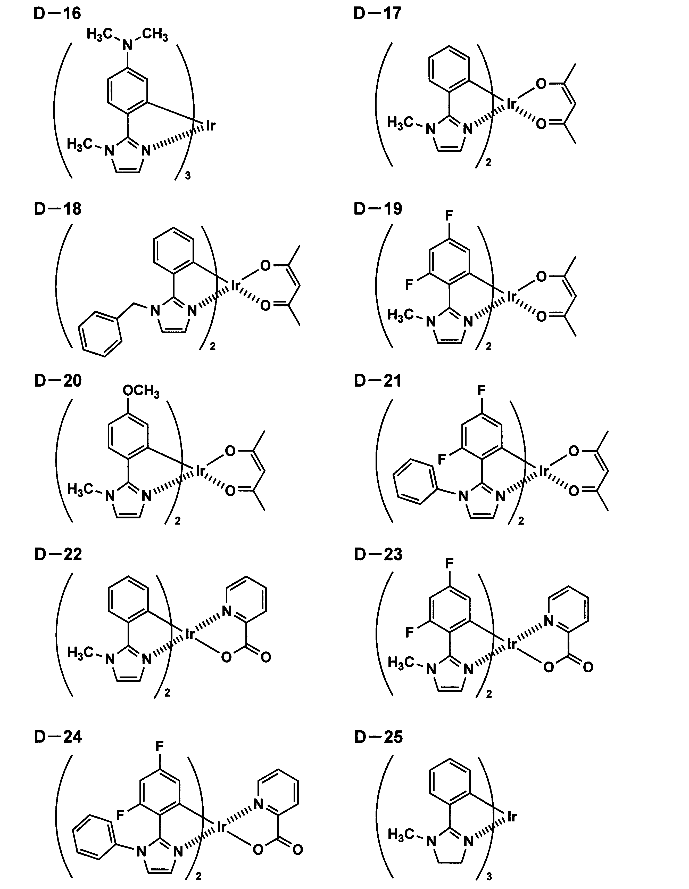
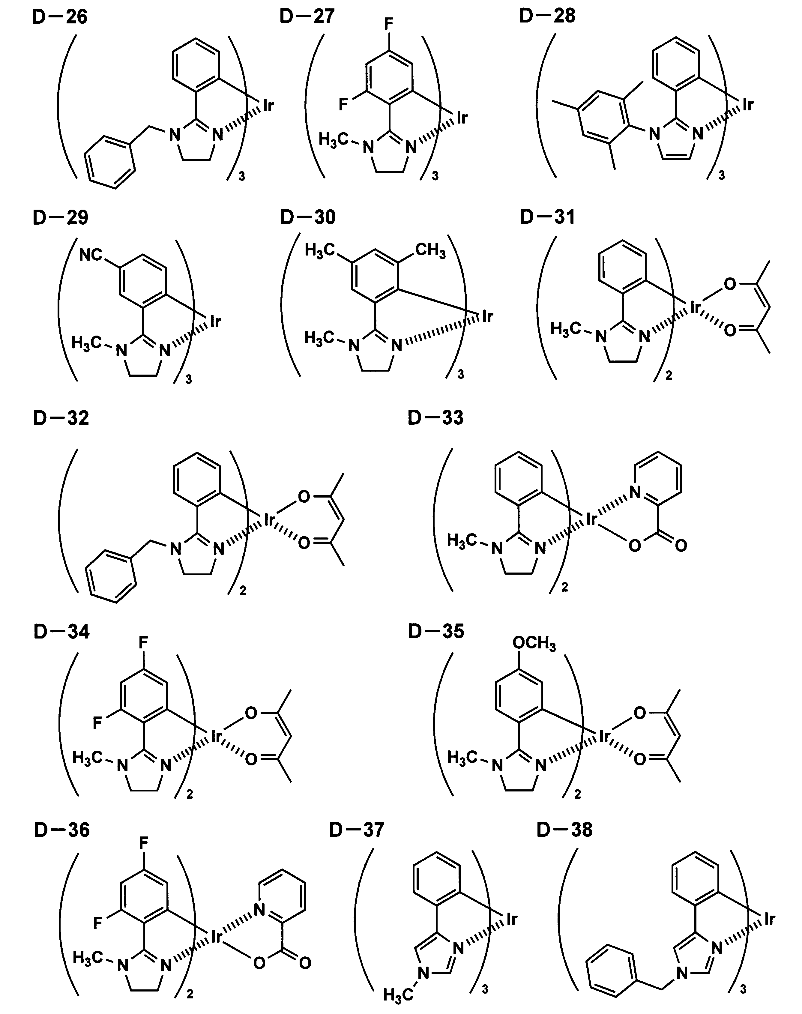
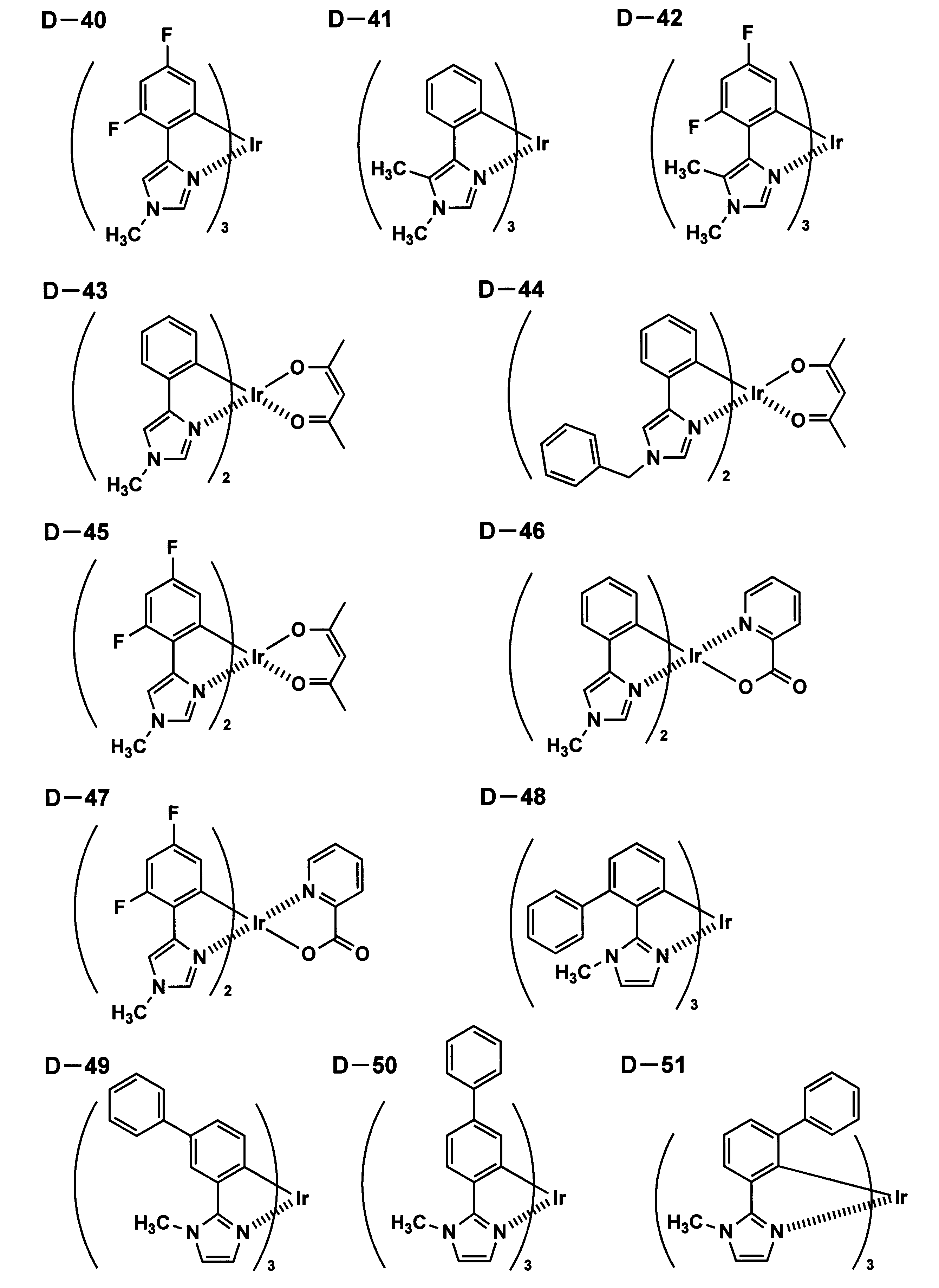

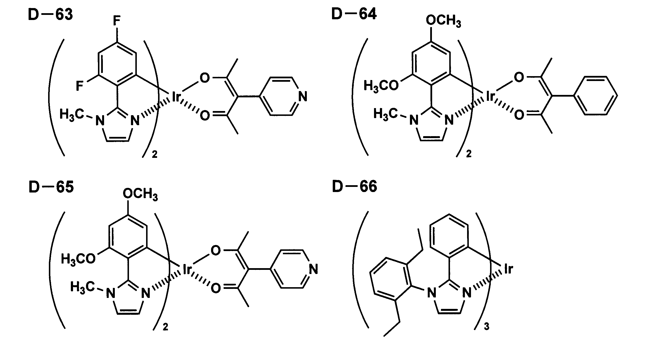

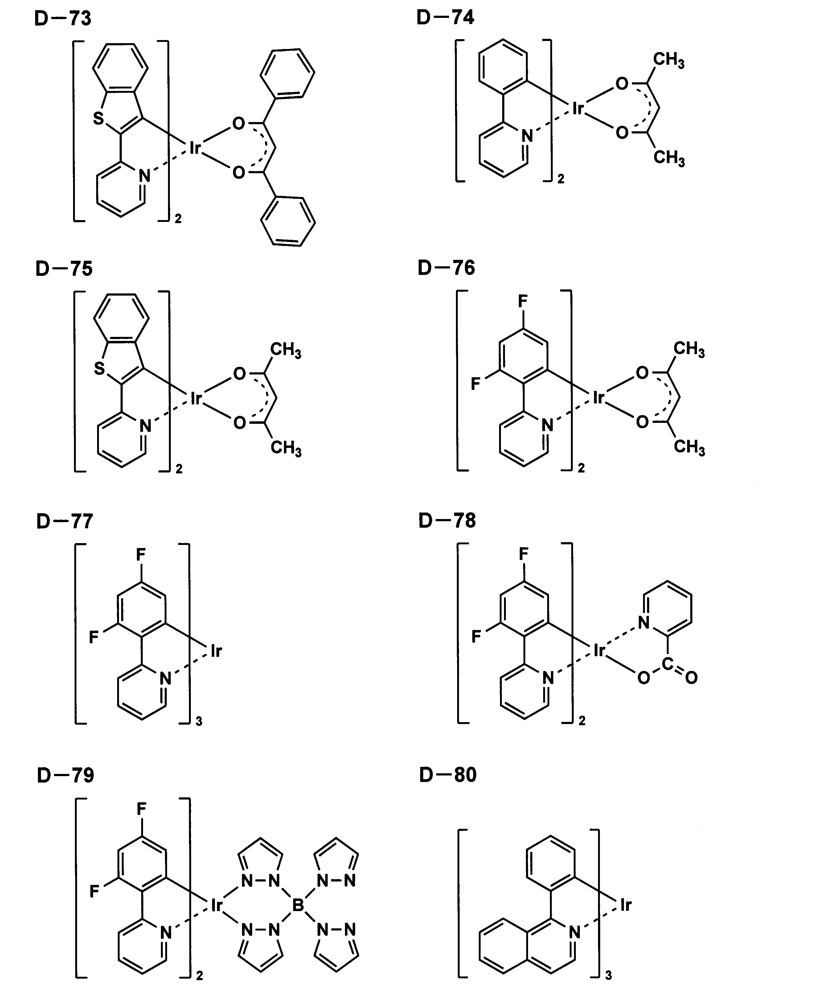

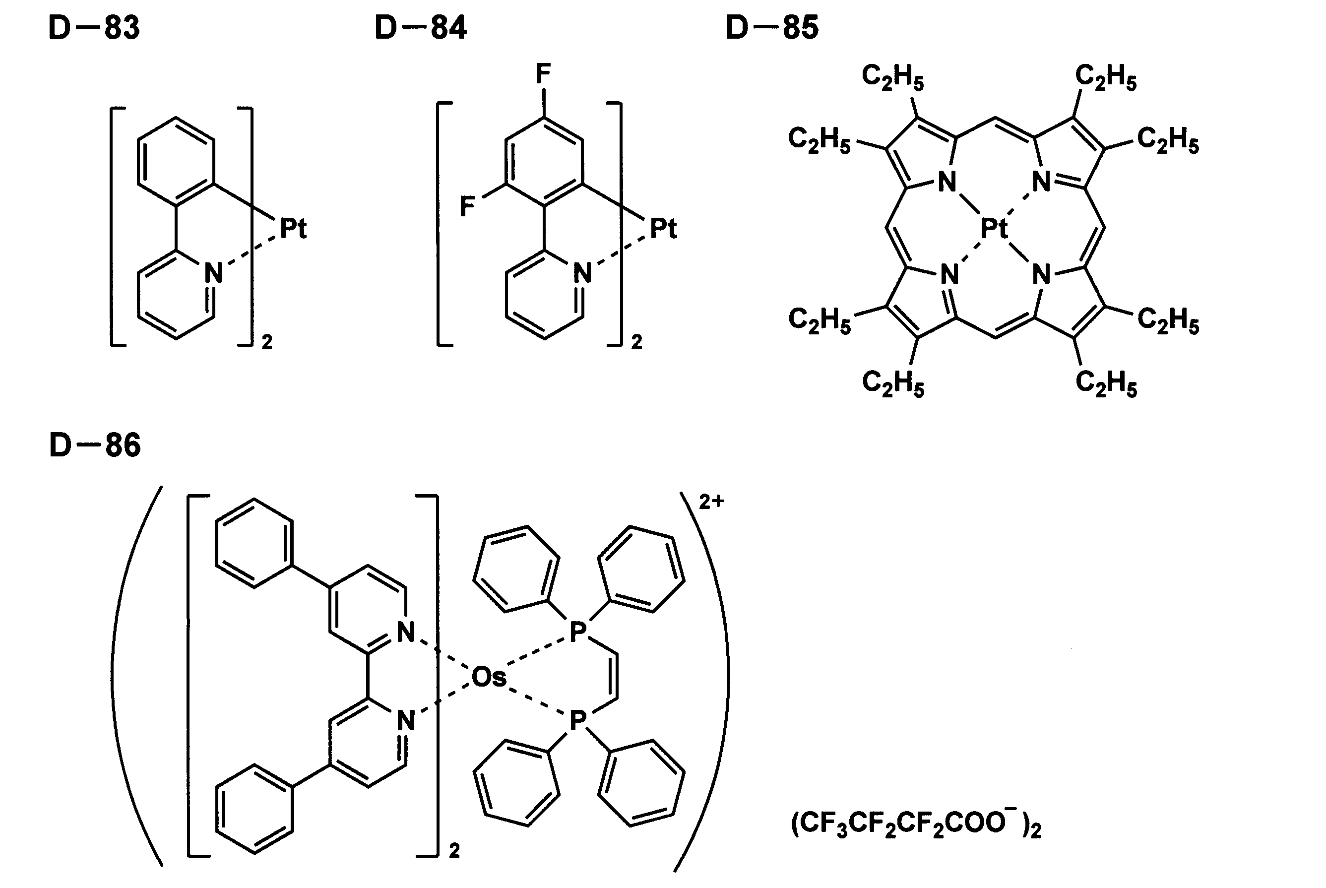
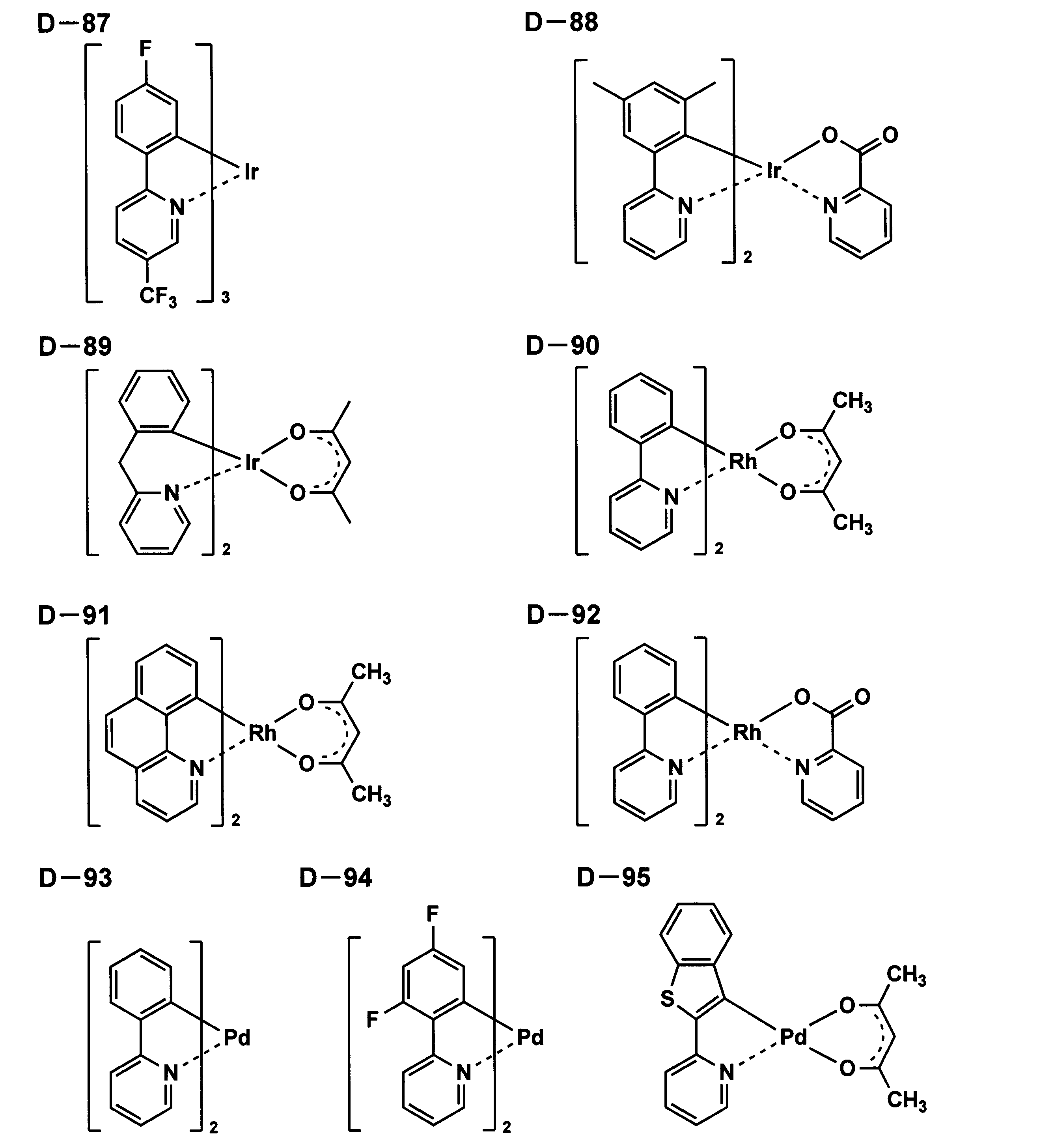


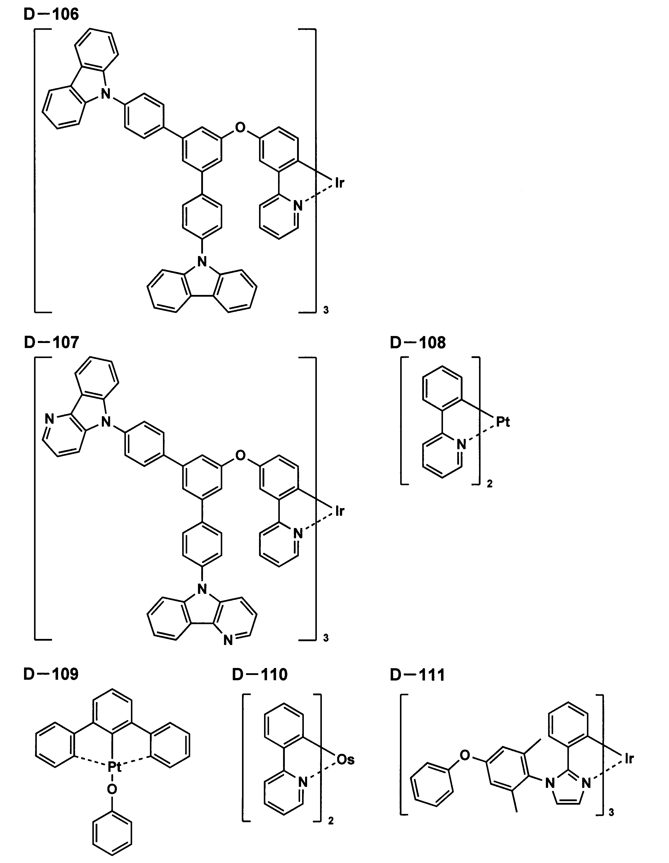
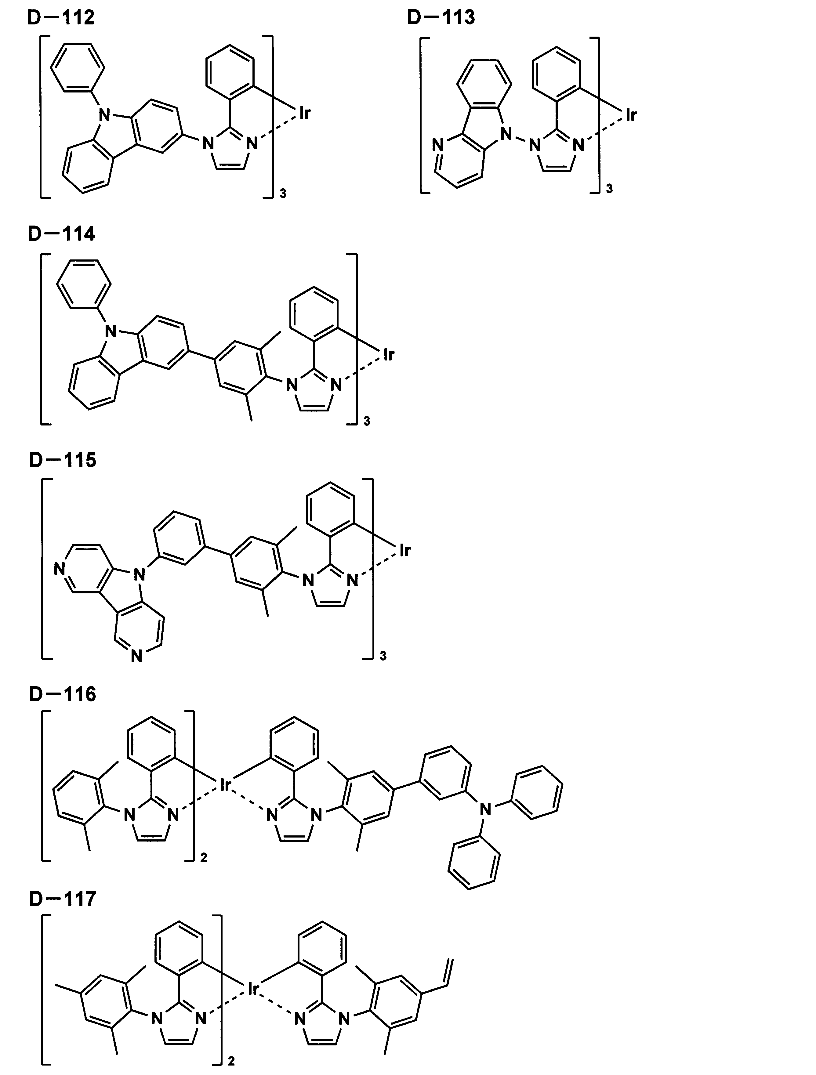

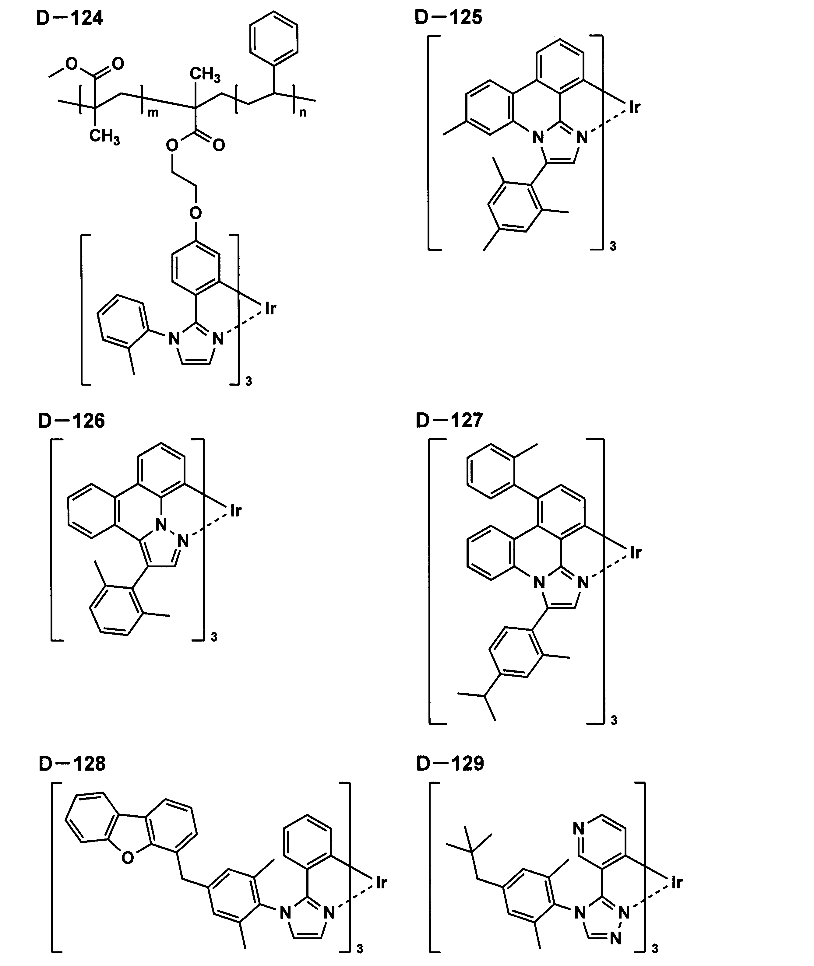
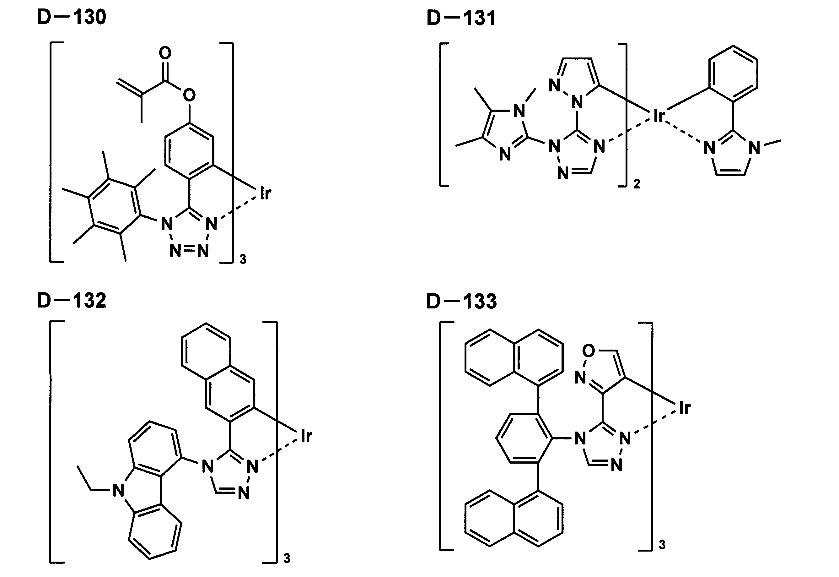
上記例示したリン光ドーパントの中でも、青色の発光波長を有する金属錯体としては、特に、下記一般式(1)で表される構造を有するイリジウム錯体を用いることが好ましい。

上記一般式(1)において、Zは、炭化水素環基又は複素環基を表す。P1-L1-P2は2座の配位子を表し、P1及びP2は各々独立に炭素原子、窒素原子、又は酸素原子を表す。L1はP1及びP2とともに2座の配位子を形成する原子群を表す。R81~R86は、各々水素原子又は置換基を表す。j1は1~3の整数を表し、j2は0~2の整数を表すが、j1+j2は2又は3である。M1は元素周期表における8族~10族の遷移金属元素を表す。
上記一般式(1)において、P1-L1-P2で表される2座の配位子としては、例えば、置換又は無置換のフェニルピリジン、フェニルピラゾール、フェニルイミダゾール、フェニルトリアゾール、フェニルテトラゾール、ピラザボール、アセチルアセトン、ピコリン酸等が挙げられる。
Zで表される炭化水素環基としては、非芳香族炭化水素環基、芳香族炭化水素環基が挙げられ、非芳香族炭化水素環基としては、シクロプロピル基、シクロペンチル基、シクロヘキシル基等が挙げられ置換されていても無置換でもよい。
また、芳香族炭化水素環基(芳香族炭化水素基、アリール基等ともいう)としては、例えば、フェニル基、p-クロロフェニル基、メシチル基、トリル基、キシリル基、ナフチル基、アントリル基、アズレニル基、アセナフテニル基、フルオレニル基、フェナントリル基、インデニル基、ピレニル基、ビフェニリル基等が挙げられる。これらの基は置換されていても無置換でもよい。
また、Zで表される複素環基としては、非芳香族複素環基、芳香族複素環基等が挙げられ、非芳香族複素環基としては、例えば、エポキシ環、アジリジン環、チイラン環、オキセタン環、アゼチジン環、チエタン環、テトラヒドロフラン環、ジオキソラン環、ピロリジン環、ピラゾリジン環、イミダゾリジン環、オキサゾリジン環、テトラヒドロチオフェン環、スルホラン環、チアゾリジン環、ε-カプロラクトン環、ε-カプロラクタム環、ピペリジン環、ヘキサヒドロピリダジン環、ヘキサヒドロピリミジン環、ピペラジン環、モルホリン環、テトラヒドロピラン環、1,3-ジオキサン環、1,4-ジオキサン環、トリオキサン環、テトラヒドロチオピラン環、チオモルホリン環、チオモルホリン-1,1-ジオキシド環、ピラノース環、ジアザビシクロ[2,2,2]-オクタン環等から誘導される基を挙げられる。
前記一般式(1)で表される構造を有する有機金属錯体において、R81~R86は各々水素原子又は置換基を表し、置換基の例としては、例えば、アルキル基(例えば、メチル基、エチル基、プロピル基、イソプロピル基、t-ブチル基、ペンチル基、ヘキシル基、オクチル基、ドデシル基、トリデシル基、テトラデシル基、ペンタデシル基等)、シクロアルキル基(例えば、シクロペンチル基、シクロヘキシル基等)、アルケニル基(例えば、ビニル基、アリル基等)、アルキニル基(例えば、エチニル基、プロパルギル基等)、芳香族炭化水素環基(芳香族炭素環基、アリール基等ともいい、例えば、フェニル基、p-クロロフェニル基、メシチル基、トリル基、キシリル基、ナフチル基、アントリル基、アズレニル基、アセナフテニル基、フルオレニル基、フェナントリル基、インデニル基、ピレニル基、ビフェニリル基等)、芳香族複素環基(例えば、ピリジル基、ピリミジニル基、フリル基、ピロリル基、イミダゾリル基、ベンゾイミダゾリル基、ピラゾリル基、ピラジニル基、トリアゾリル基(例えば、1,2,4-トリアゾール-1-イル基、1,2,3-トリアゾール-1-イル基)、オキサゾリル基、ベンゾオキサゾリル基、チアゾリル基、イソオキサゾリル基、イソチアゾリル基、フラザニル基、チエニル基、キノリル基、ベンゾフリル基、ジベンゾフリル基、ベンゾチエニル基、ジベンゾチエニル基、インドリル基、カルバゾリル基、カルボリニル基、ジアザカルバゾリル基(前記カルボリニル基のカルボリン環を構成する炭素原子の一つが窒素原子で置き換わったものを示す。)、キノキサリニル基、ピリダジニル基、トリアジニル基、キナゾリニル基、フタラジニル基等)、複素環基(例えば、ピロリジル基、イミダゾリジル基、モルホリル基、オキサゾリジル基等)、アルコキシ基(例えば、メトキシ基、エトキシ基、プロピルオキシ基、ペンチルオキシ基、ヘキシルオキシ基、オクチルオキシ基、ドデシルオキシ基等)、シクロアルコキシ基(例えば、シクロペンチルオキシ基、シクロヘキシルオキシ基等)、アリールオキシ基(例えば、フェノキシ基、ナフチルオキシ基等)、アルキルチオ基(例えば、メチルチオ基、エチルチオ基、プロピルチオ基、ペンチルチオ基、ヘキシルチオ基、オクチルチオ基、ドデシルチオ基等)、シクロアルキルチオ基(例えば、シクロペンチルチオ基、シクロヘキシルチオ基等)、アリールチオ基(例えば、フェニルチオ基、ナフチルチオ基等)、アルコキシカルボニル基(例えば、メチルオキシカルボニル基、エチルオキシカルボニル基、ブチルオキシカルボニル基、オクチルオキシカルボニル基、ドデシルオキシカルボニル基等)、アリールオキシカルボニル基(例えば、フェニルオキシカルボニル基、ナフチルオキシカルボニル基等)、スルファモイル基(例えば、アミノスルホニル基、メチルアミノスルホニル基、ジメチルアミノスルホニル基、ブチルアミノスルホニル基、ヘキシルアミノスルホニル基、シクロヘキシルアミノスルホニル基、オクチルアミノスルホニル基、ドデシルアミノスルホニル基、フェニルアミノスルホニル基、ナフチルアミノスルホニル基、2-ピリジルアミノスルホニル基等)、アシル基(例えば、アセチル基、エチルカルボニル基、プロピルカルボニル基、ペンチルカルボニル基、シクロヘキシルカルボニル基、オクチルカルボニル基、2-エチルヘキシルカルボニル基、ドデシルカルボニル基、フェニルカルボニル基、ナフチルカルボニル基、ピリジルカルボニル基等)、アシルオキシ基(例えば、アセチルオキシ基、エチルカルボニルオキシ基、ブチルカルボニルオキシ基、オクチルカルボニルオキシ基、ドデシルカルボニルオキシ基、フェニルカルボニルオキシ基)、アミド基(例えば、メチルカルボニルアミノ基、エチルカルボニルアミノ基、ジメチルカルボニルアミノ基、プロピルカルボニルアミノ基、ペンチルカルボニルアミノ基、シクロヘキシルカルボニルアミノ基、2-エチルヘキシルカルボニルアミノ基、オクチルカルボニルアミノ基、ドデシルカルボニルアミノ基、フェニルカルボニルアミノ基、ナフチルカルボニルアミノ基等)、カルバモイル基(例えば、アミノカルボニル基、メチルアミノカルボニル基、ジメチルアミノカルボニル基、プロピルアミノカルボニル基、ペンチルアミノカルボニル基、シクロヘキシルアミノカルボニル基、オクチルアミノカルボニル基、2-エチルヘキシルアミノカルボニル基、ドデシルアミノカルボニル基、フェニルアミノカルボニル基、ナフチルアミノカルボニル基、2-ピリジルアミノカルボニル基等)、ウレイド基(例えば、メチルウレイド基、エチルウレイド基、ペンチルウレイド基、シクロヘキシルウレイド基、オクチルウレイド基、ドデシルウレイド基、フェニルウレイド基ナフチルウレイド基、2-ピリジルアミノウレイド基等)、スルフィニル基(例えば、メチルスルフィニル基、エチルスルフィニル基、ブチルスルフィニル基、シクロヘキシルスルフィニル基、2-エチルヘキシルスルフィニル基、ドデシルスルフィニル基、フェニルスルフィニル基、ナフチルスルフィニル基、2-ピリジルスルフィニル基等)、アルキルスルホニル基(例えば、メチルスルホニル基、エチルスルホニル基、ブチルスルホニル基、シクロヘキシルスルホニル基、2-エチルヘキシルスルホニル基、ドデシルスルホニル基等)、アリールスルホニル基又はヘテロアリールスルホニル基(例えば、フェニルスルホニル基、ナフチルスルホニル基、2-ピリジルスルホニル基等)、アミノ基(例えば、アミノ基、エチルアミノ基、ジメチルアミノ基、ブチルアミノ基、シクロペンチルアミノ基、2-エチルヘキシルアミノ基、ドデシルアミノ基、アニリノ基、ナフチルアミノ基、2-ピリジルアミノ基等)、ハロゲン原子(例えば、フッ素原子、塩素原子、臭素原子等)、フッ化炭化水素基(例えば、フルオロメチル基、トリフルオロメチル基、ペンタフルオロエチル基、ペンタフルオロフェニル基等)、シアノ基、ニトロ基、ヒドロキシ基、メルカプト基、シリル基(例えば、トリメチルシリル基、トリイソプロピルシリル基、トリフェニルシリル基、フェニルジエチルシリル基等)が挙げられる。これらの置換基は、更に、上記の置換基によって置換されていてもよい。これらの置換基は複数が互いに結合して環を形成していてもよい。
中でも、芳香族炭化水素環基(芳香族炭素環基、アリール基等ともいい、例えば、フェニル基、p-クロロフェニル基、メシチル基、トリル基、キシリル基、ナフチル基、アントリル基、アズレニル基、アセナフテニル基、フルオレニル基、フェナントリル基、インデニル基、ピレニル基、ビフェニリル基等)又は、芳香族複素環基(例えば、フリル基、チエニル基、ピリジル基、ピリダジニル基、ピリミジニル基、ピラジニル基、トリアジニル基、イミダゾリル基、ピラゾリル基、チアゾリル基、キナゾリニル基、フタラジニル基等)が特に好ましい。
また、本発明において、発光層に金属錯体化合物を含む場合、発光層に含まれる金属錯体化合物は一種類でも良いし、異なる発光極大波長を持つ二種類以上の金属錯体化合物を含有させても良い。また、発光材料を複数種用いることで、異なる発光を混色することが可能となり、これにより、白色を含む任意の発光色を得ることができる。本発明においては、発光層が分子量2000以下の発光ドーパントを含有することが好ましい。
本発明に係る有機EL素子の発光層に含有されるホスト化合物としては、室温(25℃)におけるリン光発光のリン光量子収率が0.1未満の化合物が好ましい。さらに好ましくはリン光量子収率が0.01未満である。また、発光層に含有される化合物の中で、その層中での体積比が50%以上であることが好ましい。
ホスト化合物としては、公知のホスト化合物を単独で用いてもよく、又は複数種併用して用いてもよい。ホスト化合物を複数種用いることで、電荷の移動を調整することが可能であり、有機EL素子を高効率化することができる。
本発明に用いられるホスト化合物としては、従来公知の低分子化合物でも、繰り返し単位をもつ高分子化合物でもよく、ビニル基やエポキシ基のような重合性基を有する低分子化合物(蒸着重合性発光ホスト)でもよいが、本発明では、発光層が、分子量が2000以下の発光ホスト化合物を用いることが好ましい。
公知のホスト化合物としては、正孔輸送能、電子輸送能を有しつつ、かつ発光の長波長化を防ぎ、なおかつ高Tg(ガラス転移温度)である化合物が好ましい。ここで、ガラス転移点(Tg)とは、DSC(Differential Scanning Colorimetry:示差走査熱量法)を用いて、JIS-K-7121に準拠した方法により求められる値である。
公知のホスト化合物の具体例としては、以下の文献に記載されている化合物が挙げられる。例えば、特開2001-257076号公報、同2002-308855号公報、同2001-313179号公報、同2002-319491号公報、同2001-357977号公報、同2002-334786号公報、同2002-8860号公報、同2002-334787号公報、同2002-15871号公報、同2002-334788号公報、同2002-43056号公報、同2002-334789号公報、同2002-75645号公報、同2002-338579号公報、同2002-105445号公報、同2002-343568号公報、同2002-141173号公報、同2002-352957号公報、同2002-203683号公報、同2002-363227号公報、同2002-231453号公報、同2003-3165号公報、同2002-234888号公報、同2003-27048号公報、同2002-255934号公報、同2002-260861号公報、同2002-280183号公報、同2002-299060号公報、同2002-302516号公報、同2002-305083号公報、同2002-305084号公報、同2002-308837号公報等が挙げられる。
本発明に用いられるホスト化合物としては、カルバゾール誘導体であることが好ましく、カルバゾール誘導体であるジベンゾフラン化合物がより好ましい。
(注入層)
本発明に係る有機EL素子において、注入層は必要に応じて設けることができる。注入層としては電子注入層と正孔注入層があり、上記の如く陽極と発光層又は正孔輸送層の間、及び陰極と発光層又は電子輸送層との間に存在させてもよい。
本発明に係る有機EL素子において、注入層は必要に応じて設けることができる。注入層としては電子注入層と正孔注入層があり、上記の如く陽極と発光層又は正孔輸送層の間、及び陰極と発光層又は電子輸送層との間に存在させてもよい。
本発明でいう注入層とは、駆動電圧低下や発光輝度向上のため、電極と有機層間に設けられる層で、「有機EL素子とその工業化最前線(1998年11月30日エヌ・ティー・エス社発行)」の第2編第2章「電極材料」(123~166頁)に、その詳細が記載されている。
正孔注入層とその構成材料については、例えば、特開平9-45479号公報、同9-260062号公報、同8-288069号公報等に、その詳細が記載されている。
正孔注入層の形成に適用可能な形成材料としては、例えば、トリアゾール誘導体、オキサジアゾール誘導体、イミダゾール誘導体、ピラゾリン誘導体及びピラゾロン誘導体、フェニレンジアミン誘導体、アリールアミン誘導体、アミノ置換カルコン誘導体、オキサゾール誘導体、スチリルアントラセン誘導体、フルオレノン誘導体、ヒドラゾン誘導体、スチルベン誘導体、シラザン誘導体等を含むポリマーやアニリン系共重合体、ポリアリールアルカン誘導体、又は導電性ポリマーが挙げられ、好ましくはポリチオフェン誘導体、ポリアニリン誘導体、ポリピローラー誘導体であり、さらに好ましくはポリチオフェン誘導体である。
電子注入層とその構成材料については、例えば、特開平6-325871号公報、同9-17574号公報、同10-74586号公報等に、その詳細が記載されている。
電子注入層の形成に適用可能な形成材料としては、金属化合物が挙げられ、具体例としては、ストロンチウムやアルミニウム等に代表される金属バッファー層、フッ化リチウムに代表されるアルカリ金属化合物バッファー層、フッ化マグネシウムに代表されるアルカリ土類金属化合物バッファー層、酸化アルミニウムに代表される酸化物バッファー層等が挙げられる。本発明においては、上記バッファー層(注入層)はごく薄い層であることが好適であり、フッ化カリウム、フッ化ナトリウムが好ましい。その層厚は0.1nmから5μm程度、好ましくは0.1~100nmの範囲内であり、さらに好ましくは0.5~10nmの範囲内、最も好ましくは0.5~4nmの範囲内である。
(正孔輸送層)
本発明に係る正孔輸送層の形成に用いることのできる正孔輸送層形成材料としては、上記正孔注入層で適用することができるのと同様の化合物を挙げることができるが、さらには、ポルフィリン化合物、芳香族第3級アミン化合物及びスチリルアミン化合物を挙げることができ、その中でも、特に、芳香族第3級アミン化合物を用いることが好ましい。
本発明に係る正孔輸送層の形成に用いることのできる正孔輸送層形成材料としては、上記正孔注入層で適用することができるのと同様の化合物を挙げることができるが、さらには、ポルフィリン化合物、芳香族第3級アミン化合物及びスチリルアミン化合物を挙げることができ、その中でも、特に、芳香族第3級アミン化合物を用いることが好ましい。
芳香族第3級アミン化合物及びスチリルアミン化合物の代表例としては、N,N,N′,N′-テトラフェニル-4,4′-ジアミノフェニル;N,N′-ジフェニル-N,N′-ビス(3-メチルフェニル)-〔1,1′-ビフェニル〕-4,4′-ジアミン(略称:TPD);2,2-ビス(4-ジ-p-トリルアミノフェニル)プロパン;1,1-ビス(4-ジ-p-トリルアミノフェニル)シクロヘキサン;N,N,N′,N′-テトラ-p-トリル-4,4′-ジアミノビフェニル;1,1-ビス(4-ジ-p-トリルアミノフェニル)-4-フェニルシクロヘキサン;ビス(4-ジメチルアミノ-2-メチルフェニル)フェニルメタン;ビス(4-ジ-p-トリルアミノフェニル)フェニルメタン;N,N′-ジフェニル-N,N′-ジ(4-メトキシフェニル)-4,4′-ジアミノビフェニル;N,N,N′,N′-テトラフェニル-4,4′-ジアミノジフェニルエーテル;4,4′-ビス(ジフェニルアミノ)クオードリフェニル;N,N,N-トリ(p-トリル)アミン;4-(ジ-p-トリルアミノ)-4′-〔4-(ジ-p-トリルアミノ)スチリル〕スチルベン;4-N,N-ジフェニルアミノ-(2-ジフェニルビニル)ベンゼン;3-メトキシ-4′-N,N-ジフェニルアミノスチルベンゼン;N-フェニルカルバゾール、更には、米国特許第5,061,569号明細書に記載されている2個の縮合芳香族環を分子内に有するもの、例えば、4,4′-ビス〔N-(1-ナフチル)-N-フェニルアミノ〕ビフェニル(略称:NPD)、特開平4-308688号公報に記載されているトリフェニルアミンユニットが三つスターバースト型に連結された4,4′,4″-トリス〔N-(3-メチルフェニル)-N-フェニルアミノ〕トリフェニルアミン(略称:MTDATA)等が挙げられる。
更に、これらの材料を高分子鎖に導入した、又はこれらの材料を高分子の主鎖とした高分子材料を用いることもできる。また、p型-Si、p型-SiC等の無機化合物も正孔注入層材料、正孔輸送層材料として使用することができる。
また、特開平4-297076号公報、特開2000-196140号公報、特開2001-102175号公報、J.Appl.Phys.,95,5773(2004)、特開平11-251067号公報、J.Huang et.al.著文献(Applied Physics Letters 80(2002),p.139)、特表2003-519432号公報に記載されているような、いわゆるp型半導体的性質を有する正孔輸送層材料を用いることもできる。
正孔輸送層の層厚については、特に制限はないが、通常は5nmから5μm程度、好ましくは5~200nmの範囲内である。正孔輸送層は、上記材料の一種又は二種以上からなる一層構造であってもよい。
(電子輸送層)
本発明でいう電子輸送層とは、電子を輸送する機能を有する材料を含有し、広い意味で電子注入層、正孔阻止層も電子輸送層に含まれる。電子輸送層は、単層又は複数層設けることができる。
本発明でいう電子輸送層とは、電子を輸送する機能を有する材料を含有し、広い意味で電子注入層、正孔阻止層も電子輸送層に含まれる。電子輸送層は、単層又は複数層設けることができる。
従来、単層の電子輸送層、あるいは複数層の電子輸送層群とする場合、発光層に対して陰極側に隣接して設けられる電子輸送層に用いる電子輸送層材料(正孔阻止層材料を兼ねる)としては、陰極より注入された電子を発光層に伝達する機能を有していればよく、そのような材料としては、従来公知の化合物の中から任意のものを選択して用いることができ、例えば、フルオレン誘導体、カルバゾール誘導体、アザカルバゾール誘導体、オキサジアゾール誘導体、トリゾール誘導体、シローラー誘導体、ピリジン誘導体、ピリミジン誘導体、8-キノリノール誘導体等の金属錯体等が挙げられる。
その他、メタルフリー若しくはメタルフタロシアニン、又はそれらの末端がアルキル基やスルホン酸基等で置換されているものも、電子輸送層材料として好ましく用いることができる。
これらの中でも、カルバゾール誘導体、アザカルバゾール誘導体、ピリジン誘導体等が本発明では好ましく、カルバゾール誘導体であるジベンゾフラン化合物がより好ましい。
電子輸送層の層厚については、特に制限はないが、通常は5nmから5μm程度、好ましくは5~200nmの範囲内である。電子輸送層は上記材料の一種又は二種以上からなる一層構造であってもよい。
また、不純物をゲスト材料としてドープした材料を、n性の高い電子輸送層に用いることもできる。その例としては、特開平4-297076号公報、同10-270172号公報、特開2000-196140号公報、同2001-102175号公報、J.Appl.Phys.,95,5773(2004)等に記載された各種材料が挙げられる。
本発明において、電子輸送層には、有機物のアルカリ金属塩を適用することが好ましい。有機物の種類としては、特に制限はないが、ギ酸塩、酢酸塩、プロピオン酸、酪酸塩、吉草酸塩、カプロン酸塩、エナント酸塩、カプリル酸塩、シュウ酸塩、マロン酸塩、コハク酸塩、安息香酸塩、フタル酸塩、イソフタル酸塩、テレフタル酸塩、サリチル酸塩、ピルビン酸塩、乳酸塩、リンゴ酸塩、アジピン酸塩、メシル酸塩、トシル酸塩、ベンゼンスルホン酸塩が挙げられ、好ましくはギ酸塩、酢酸塩、プロピオン酸塩、酪酸塩、吉草酸塩、カプロン酸塩、エナント酸塩、カプリル酸塩、シュウ酸塩、マロン酸塩、コハク酸塩、安息香酸塩、より好ましくはギ酸塩、酢酸塩、プロピオン酸塩、酪酸塩等の脂肪族カルボン酸のアルカリ金属塩が好ましく、脂肪族カルボン酸の炭素数が4以下であることが好ましい。最も好ましくは酢酸塩である。
上記有機物のアルカリ金属塩のアルカリ金属の種類としては、特に制限はないが、Na、K、Csが挙げられ、好ましくはK、Cs、さらに好ましくはCsである。有機物のアルカリ金属塩としては、前記有機物とアルカリ金属の組み合わせが挙げられ、好ましくは、ギ酸Li、ギ酸K、ギ酸Na、ギ酸Cs、酢酸Li、酢酸K、酢酸Na、酢酸Cs、プロピオン酸Li、プロピオン酸Na、プロピオン酸K、プロピオン酸Cs、シュウ酸Li、シュウ酸Na、シュウ酸K、シュウ酸Cs、マロン酸Li、マロン酸Na、マロン酸K、マロン酸Cs、コハク酸Li、コハク酸Na、コハク酸K、コハク酸Cs、安息香酸Li、安息香酸Na、安息香酸K、安息香酸Cs、より好ましくは酢酸Li、酢酸K、酢酸Na、酢酸Cs、最も好ましくは酢酸Csである。
これらドープ材料の含有量は、添加する電子輸送層に対し、好ましくは1.5~35質量%の範囲内であり、より好ましくは3~25質量%の範囲内であり、最も好ましくは5~15質量%の範囲内である。
〔陽極〕
本発明に係る有機EL素子を構成する陽極としては、仕事関数の大きい(4eV以上)金属、合金、電気伝導性化合物及びこれらの混合物を電極物質とするものが好ましく用いられる。このような電極物質の具体例としては、Au等の金属、CuI、インジウムチンオキシド(略称:ITO)、SnO2、ZnO等の導電性透明材料が挙げられる。また、IDIXO(In2O3-ZnO)等非晶質で透明導電膜を作製可能な材料を用いてもよい。陽極は、これらの電極物質を蒸着やスパッタリング等の方法により薄膜を形成させ、フォトリソグラフィー法で所望のパターンを形成してもよく、あるいはパターン精度をあまり必要としない場合、例えば、要求精度が100μm以上程度である場合には、上記電極物質の蒸着やスパッタリング時に所望の形状のマスクを介してパターンを形成してもよい。あるいは、有機導電性化合物のように塗布可能な物質を用いる場合には、印刷方式、ウェットコーティング方式等の湿式成膜法を用いることもできる。この陽極形成面より発光を取り出す場合には、陽極としては、透過率を10%以上とすることが望ましく、また陽極としてのシート抵抗は、数百Ω/□以下が好ましい。更に膜厚は材料にもよるが、通常は、10~1000nmの範囲内であり、好ましくは10~200nmの範囲内で選ばれる。
本発明に係る有機EL素子を構成する陽極としては、仕事関数の大きい(4eV以上)金属、合金、電気伝導性化合物及びこれらの混合物を電極物質とするものが好ましく用いられる。このような電極物質の具体例としては、Au等の金属、CuI、インジウムチンオキシド(略称:ITO)、SnO2、ZnO等の導電性透明材料が挙げられる。また、IDIXO(In2O3-ZnO)等非晶質で透明導電膜を作製可能な材料を用いてもよい。陽極は、これらの電極物質を蒸着やスパッタリング等の方法により薄膜を形成させ、フォトリソグラフィー法で所望のパターンを形成してもよく、あるいはパターン精度をあまり必要としない場合、例えば、要求精度が100μm以上程度である場合には、上記電極物質の蒸着やスパッタリング時に所望の形状のマスクを介してパターンを形成してもよい。あるいは、有機導電性化合物のように塗布可能な物質を用いる場合には、印刷方式、ウェットコーティング方式等の湿式成膜法を用いることもできる。この陽極形成面より発光を取り出す場合には、陽極としては、透過率を10%以上とすることが望ましく、また陽極としてのシート抵抗は、数百Ω/□以下が好ましい。更に膜厚は材料にもよるが、通常は、10~1000nmの範囲内であり、好ましくは10~200nmの範囲内で選ばれる。
〔陰極〕
陰極としては、仕事関数の小さい(4eV以下)金属(以下、電子注入性金属と称す。)、合金、電気伝導性化合物及びこれらの混合物を電極物質とするものが用いられる。このような電極物質の具体例としては、ナトリウム、ナトリウム-カリウム合金、マグネシウム、リチウム、マグネシウム/銅混合物、マグネシウム/銀混合物、マグネシウム/アルミニウム混合物、マグネシウム/インジウム混合物、アルミニウム/酸化アルミニウム(Al2O3)混合物、インジウム、リチウム/アルミニウム混合物、希土類金属等が挙げられる。これらの中で、電子注入性及び酸化等に対する耐久性の点から、電子注入性金属とこれより仕事関数の値が大きく安定な金属である第二金属との混合物、例えば、マグネシウム/銀混合物、マグネシウム/アルミニウム混合物、マグネシウム/インジウム混合物、アルミニウム/酸化アルミニウム(Al2O3)混合物、リチウム/アルミニウム混合物、アルミニウム等が好適である。陰極はこれらの電極物質を蒸着やスパッタリング等の方法により薄膜を形成させることにより、作製することができる。また、陰極としてのシート抵抗は数百Ω/□以下が好ましく、膜厚は通常10nm~5μmの範囲内、好ましくは50~200nmの範囲内で選ばれる。なお、発光した光を透過させるため、有機EL素子の陽極又は陰極のいずれか一方が透明又は半透明であることが、発光輝度が向上する点で好都合である。
陰極としては、仕事関数の小さい(4eV以下)金属(以下、電子注入性金属と称す。)、合金、電気伝導性化合物及びこれらの混合物を電極物質とするものが用いられる。このような電極物質の具体例としては、ナトリウム、ナトリウム-カリウム合金、マグネシウム、リチウム、マグネシウム/銅混合物、マグネシウム/銀混合物、マグネシウム/アルミニウム混合物、マグネシウム/インジウム混合物、アルミニウム/酸化アルミニウム(Al2O3)混合物、インジウム、リチウム/アルミニウム混合物、希土類金属等が挙げられる。これらの中で、電子注入性及び酸化等に対する耐久性の点から、電子注入性金属とこれより仕事関数の値が大きく安定な金属である第二金属との混合物、例えば、マグネシウム/銀混合物、マグネシウム/アルミニウム混合物、マグネシウム/インジウム混合物、アルミニウム/酸化アルミニウム(Al2O3)混合物、リチウム/アルミニウム混合物、アルミニウム等が好適である。陰極はこれらの電極物質を蒸着やスパッタリング等の方法により薄膜を形成させることにより、作製することができる。また、陰極としてのシート抵抗は数百Ω/□以下が好ましく、膜厚は通常10nm~5μmの範囲内、好ましくは50~200nmの範囲内で選ばれる。なお、発光した光を透過させるため、有機EL素子の陽極又は陰極のいずれか一方が透明又は半透明であることが、発光輝度が向上する点で好都合である。
また、陰極として上記金属を1~20nmの膜厚範囲内で作製した後、陽極の説明で挙げた導電性透明材料をその上に形成することで、透明又は半透明の陰極を作製することができ、これを応用することで陽極と陰極の両方が透過性を有する有機EL素子を作製することができる。
《有機エレクトロルミネッセンス素子の具体的な製造方法》
本発明の有機EL素子の製造方法の一例として、陽極/正孔注入層/正孔輸送層/発光層/電子輸送層/電子注入層/陰極から構成される有機EL素子の製造方法について説明する。
本発明の有機EL素子の製造方法の一例として、陽極/正孔注入層/正孔輸送層/発光層/電子輸送層/電子注入層/陰極から構成される有機EL素子の製造方法について説明する。
本発明の有機EL素子の製造方法の第1の方法においては、正孔注入層、正孔輸送層、発光層、電子輸送層から構成される有機層ユニットは、各有機層の形成材料を溶媒に溶解して調製した各有機層形成用塗布液を逐次塗布することで形成され、前記正孔注入層、正孔輸送層、発光層及び電子輸送層の各有機層の形成に用いる塗布液が含有する溶媒のうち、最も高い沸点を有する溶媒を含む有機層を形成した後、前記陰極を形成するまでの間の工程で、下記式(a)で規定する加熱処理温度で1回の加熱処理を施すことを特徴とする。
式(a):(有機層である正孔注入層、正孔輸送層、発光層、電子輸送層及び電子注入層の形成に用いる溶媒のうち、最も高い沸点を有する溶媒の沸点-10℃)≦(加熱処理温度)≦(透明樹脂フィルム基材のガラス転移温度(Tg)+20℃)
例えば、正孔注入層、正孔輸送層、発光層、電子輸送層に用いられる溶媒のうち、正孔輸送層の溶媒沸点が最も高い場合は、正孔輸送層を塗布成膜した後、陰極の形成までの間に上記式(a)の条件で一括加熱処理する方法であり、また、発光層形成用塗布液が含有する溶媒の沸点が最も高い場合は、発光層を塗布成膜後、陰極形成までの間に上記式(a)を満たす条件で一括加熱処理される。
例えば、正孔注入層、正孔輸送層、発光層、電子輸送層に用いられる溶媒のうち、正孔輸送層の溶媒沸点が最も高い場合は、正孔輸送層を塗布成膜した後、陰極の形成までの間に上記式(a)の条件で一括加熱処理する方法であり、また、発光層形成用塗布液が含有する溶媒の沸点が最も高い場合は、発光層を塗布成膜後、陰極形成までの間に上記式(a)を満たす条件で一括加熱処理される。
本発明においては、更には、上記式(a)で規定する加熱処理温度で一括加熱処理する工程が、最終の有機層、例えば、電子注入層を形成した後で、前記陰極を形成する前の工程であることが好ましい態様である。
第1の製造方法による有機EL素子の作製方法をより具体的に説明すると、
(1):例えば、樹脂フィルム基材として、ポリエチレンテレフタレートフィルム(以降、PETと略記、Tg:110℃)を用い、その上に、本発明で規定する元素組成プロファイルを有するガスバリアー層を、磁場を有するローラー間に放電空間を有する放電プラズマ化学気相成長法により形成して、ガスバリアー性フィルムを作製する。
(1):例えば、樹脂フィルム基材として、ポリエチレンテレフタレートフィルム(以降、PETと略記、Tg:110℃)を用い、その上に、本発明で規定する元素組成プロファイルを有するガスバリアー層を、磁場を有するローラー間に放電空間を有する放電プラズマ化学気相成長法により形成して、ガスバリアー性フィルムを作製する。
(2):次いで、陽極を公知の方法で形成した後、溶媒Aを含む正孔注入層形成用塗布液を用いて正孔注入層を形成し、自然乾燥する。
(3):次いで、溶媒Bを含む正孔輸送層形成用塗布液を用いて正孔輸送層を形成し、自然乾燥する。
(4):次いで、溶媒Cを含む発光層形成用塗布液を用いて発光層を形成し、自然乾燥する。
(5):最後に、溶媒Dを含む電子輸送層形成用塗布液を用いて電子輸送層を形成する。
(6):次いで、式(a)で規定する条件である、各有機層の形成で用いた溶媒A~Dのうち、最も沸点が高い溶媒の沸点を基準として、最も沸点が高い溶媒の沸点-10℃以上で、かつ樹脂フィルム基材のTg+20℃、上記のPETの場合には、110℃+20℃=130℃以下の温度範囲で、1回の加熱処理を施すことを特徴とする方法である。
すなわち、本発明においては、加熱処理温度の下限は、正孔注入層、正孔輸送層、発光層及び電子輸送層の形成に用いられている溶媒のうち、最も高い沸点を有する溶媒の沸点から10℃低い温度であり、上限は、使用している透明樹脂フィルム基材のガラス転移温度(Tg)から20℃高い温度である。すなわち、いずれの層の形成後に加熱処理を行う場合でも、その加熱温度の上限は、使用している透明樹脂フィルム基材のガラス転移温度(Tg)+20℃を超えることはない。
上記式(a)の条件で加熱処理する時の加熱時間としては、適用する加熱温度により変化するものであり、一様には規定することはできないが、おおむね10~120分の範囲であり、生産性を考慮すると、15~80分の範囲内が好ましく、更に好ましくは15~60分の範囲内である。
本発明の有機EL素子の製造方法の第2の方法は、正孔注入層、正孔輸送層、発光層及び電子輸送層の各形成材料を溶媒に溶解して調製した各有機層塗布液を逐次塗布する際に、正孔注入層、正孔輸送層、発光層及び電子輸送層のそれぞれの塗布を行った後に、下記に示す式(b)で規定する加熱処理温度で加熱処理することを特徴とする製造方法である。
式(b):(当該有機層形成用塗布液を構成する溶媒の沸点-10℃)≦(加熱処理温度)≦(透明樹脂フィルム基材のガラス転移温度(Tg)+20℃)
本発明では、各有機層を塗布形成した後に、その都度、上記式(b)で規定する加熱処理温度条件で加熱処理することを特徴とするものである。従って、この製造方法では、有機層の層数と同数で、式(b)で規定する加熱処理温度で加熱処理が施される。
本発明では、各有機層を塗布形成した後に、その都度、上記式(b)で規定する加熱処理温度条件で加熱処理することを特徴とするものである。従って、この製造方法では、有機層の層数と同数で、式(b)で規定する加熱処理温度で加熱処理が施される。
なお、有機層が複数種の溶媒を含有している場合には、「当該有機層形成用塗布液を構成する溶媒の沸点」とは、その中でも最も高い沸点を有する溶媒の沸点である。
上記式(b)で規定する第2の製造方法による有機EL素子の作製方法を具体的に説明すると、
(1):例えば、透明樹脂フィルム基材として、ポリエチレンテレフタレートフィルム(PETと略記、Tg:110℃)を用い、その上に、本発明で規定する元素組成プロファイルを有するガスバリアー層を、磁場を有するローラー間に放電空間を有する放電プラズマ化学気相成長法により形成して、ガスバリアー性フィルムを作製する。
(1):例えば、透明樹脂フィルム基材として、ポリエチレンテレフタレートフィルム(PETと略記、Tg:110℃)を用い、その上に、本発明で規定する元素組成プロファイルを有するガスバリアー層を、磁場を有するローラー間に放電空間を有する放電プラズマ化学気相成長法により形成して、ガスバリアー性フィルムを作製する。
(2):次いで、陽極を公知の方法で形成した後、第1の工程として溶媒Aを含む正孔注入層形成用塗布液を用いて、正孔注入層を形成した後、式(b)の条件である(溶媒Aの沸点-10℃)以上の温度で、かつ(樹脂フィルム基材のTg+20℃)以下の温度範囲で第1回目の加熱処理を行う。
(3):次いで、溶媒Bを含む正孔輸送層形成用塗布液を用いて、正孔輸送層を形成した後、式(b)の条件である(溶媒Bの沸点-10℃)以上で、かつ(樹脂フィルム基材のTg+20℃)以下の温度範囲で第2回目の加熱処理を行う。
(4):次いで、溶媒Cを含む発光層形成用塗布液を用いて、発光層を形成した後、式(b)の条件である(溶媒Cの沸点-10℃)以上の温度で、かつ(樹脂フィルム基材のTg+20℃)以下の温度範囲で第3回目の加熱処理を行う。
(5):最後に、溶媒Dを含む電子輸送層形成用塗布液を用いて、電子輸送層を形成した後、式(b)の条件である(溶媒Dの沸点-10℃)以上の温度で、かつ(樹脂フィルム基材のTg+20℃)以下の温度範囲で第4回目の加熱処理を行うことを特徴とする方法である。
なお、有機層が複数種の溶媒を含有している場合には、本発明でいう「有機層形成用塗布液を構成する溶媒の沸点を規定する溶媒」とは、その中で最も高い沸点を有する溶媒とする。
上記式(b)の条件で加熱処理する時の加熱時間としては、適用する加熱温度により一概には規定することはできないが、おおむね10~120分の範囲であり、生産性を考慮すると、15~80分の範囲内が好ましく、更に好ましくは15~60分の範囲内である。
上記第2の製造方法においても、各有機層の形成後に施す加熱処理温度の上限は、使用している透明樹脂フィルム基材のガラス転移温度(Tg)+20℃未満の温度である。すなわち、本発明においては、いかなる加熱処理であっても、その上限温度は、使用している透明樹脂フィルム基材のガラス転移温度(Tg)+20℃の温度を超えることはない。
本発明において、正孔注入層、正孔輸送層、発光層、電子輸送層を含む各有機層は、各有機層の形成材料を溶媒に溶解して調製した各塗布液を逐次塗布することで形成されるが、形成方法としては、特に限定されないが、例えば、スピンコート法、キャスト法、ダイコート法、ブレードコート法、ローラーコート法、インクジェット法、印刷法、スプレーコート法、カーテンコート法、LB法(ラングミュア・ブロジェット(Langmuir Blodgett)法)等を挙げることができる)が好ましく、生産性の観点からスリットダイコーターを用いるダイコート法がより好ましい。
また、加熱処理の方法としては、特に限定されないが、高温環境内を通過させて加熱する方法、ヒートブロック等の発熱体に基材を接触させ熱伝導により有機層を有する基材を加熱する方法、抵抗線等による外部ヒーターにより雰囲気を加熱する方法、IRヒーターのような赤外領域の光を用いた方法等が挙げられる。特に、溶媒を効果的に除去させるために、減圧下で加熱処理する方法が好ましい。また、基材を加熱する際には、基材側から加熱することが好ましい。更には、加熱の開始タイミングは特に限定されないが、塗布液を基材上に塗布してから1時間以内に、加熱処理を開始することが好ましい。加熱する時間としては1秒から10時間の範囲が好ましく、10秒から1時間の範囲で加熱することが更に好ましい。
〔封止材料〕
本発明に係る有機EL素子の封止に適用可能な封止材料としては、可撓性部材を使用することが好ましく、可撓性部材としては、樹脂フィルム上にガスバリアー層を有するものが好ましい。ガスバリアー層の特性としては、水蒸気透過度は、有機層の結晶化、電極の剥離等によりダークスポットの発生、及び有機EL素子の長寿命化等を考慮し、0.01g/m2・day以下であることが好ましい。水蒸気透過度はJIS K7129B法(1992年)に準拠した方法で主としてMOCON法により測定した値を示す。
本発明に係る有機EL素子の封止に適用可能な封止材料としては、可撓性部材を使用することが好ましく、可撓性部材としては、樹脂フィルム上にガスバリアー層を有するものが好ましい。ガスバリアー層の特性としては、水蒸気透過度は、有機層の結晶化、電極の剥離等によりダークスポットの発生、及び有機EL素子の長寿命化等を考慮し、0.01g/m2・day以下であることが好ましい。水蒸気透過度はJIS K7129B法(1992年)に準拠した方法で主としてMOCON法により測定した値を示す。
酸素透過度は、有機層の結晶化、第2電極の剥離等によるダークスポットの発生、及び有機EL素子の長寿命化等を考慮し、0.01ml/m2・day・atm以下であることが好ましい。酸素透過度はJIS K7126B法(1987年)に準拠した方法で主としてMOCON法により測定した値である。
使用する可撓性部材の厚さは、製造時の取扱い性、引っ張り強さやガスバリアー層のストレスクラッキング耐性等を考慮し、10~300μmの範囲内が好ましい。厚さは、マイクロメータを使用し、縦方向、幅方向で各10箇所を測定した値の平均値で示す。
本発明において、可撓性部材を構成している樹脂基材としては特に限定はなく、前述の本発明に係るガスバリアー層を有する透明樹脂フィルム基材を使用することもできる。
ガスバリアー層としては、無機蒸着膜、金属箔が挙げられる。無機蒸着膜としては薄膜ハンドブックp879~p901(日本学術振興会)、真空技術ハンドブックp502~p509、p612、p810(日刊工業新聞社)、真空ハンドブック増訂版p132~p134(ULVAC 日本真空技術K.K)に記載されている無機膜が挙げられる。例えば、In、Sn、Pb、Au、Cu、Ag、Al、Ti、Ni等の金属、MgO、SiO、SiO2、Al2O3、GeO、NiO、CaO、BaO、Fe2O3、Y2O3、TiO2、Cr2O3、SixOy(x=1、y=1.5~2.0)、Ta2O3、ZrN、SiC、TiC、PSG、Si3N4、SiN、単結晶Si、アモルファスSi、W、等が用いられる。
また、金属箔の材料としては、例えば、アルミニウム、銅、ニッケル等の金属材料や、ステンレス、アルミニウム合金等の合金材料を用いることができるが、加工性やコストの面でアルミニウムが好ましい。膜厚は、1~100μm程度、好ましくは10~50μm程度が望ましい。
使用する金属シートの厚さは、製造時の取扱い性及びパネルの薄膜化を考慮し、20μm~2mmの範囲内が好ましい。厚さは、マイクロメータを使用し、縦方向、幅方向で各10箇所を測定した平均値を示す。構成金属としては特に限定はなく、例えば、アルミニウム、銅、ニッケル等の金属材料や、ステンレス、アルミニウム合金等の合金材料等が挙げられる。
また、ガスバリアー層上には、必要に応じて保護層等を設けてもよい。
樹脂基材は単体構成でもよいし、異なる樹脂材料から構成される複合体であってもよく、必要に応じて適宜選択することが可能である。また、ガスバリアー層は単層でもよいし、2層以上が積層された構成であってもよく、必要に応じて適宜選択することが可能である。
《有機EL素子の用途》
本発明に係る有機EL素子は、表示デバイス、ディスプレイ、各種発光光源として用いることができる。発光光源として、例えば、家庭用照明、車内照明、時計や液晶用のバックライト、看板広告、信号機、光記憶媒体の光源、電子写真複写機の光源、光通信処理機の光源、光センサーの光源、さらには表示装置を必要とする一般の家庭用電気器具等広い範囲の用途が挙げられるが、特にカラーフィルターと組み合わせた液晶表示装置のバックライト、照明用光源としての用途に有効に用いることができる。
本発明に係る有機EL素子は、表示デバイス、ディスプレイ、各種発光光源として用いることができる。発光光源として、例えば、家庭用照明、車内照明、時計や液晶用のバックライト、看板広告、信号機、光記憶媒体の光源、電子写真複写機の光源、光通信処理機の光源、光センサーの光源、さらには表示装置を必要とする一般の家庭用電気器具等広い範囲の用途が挙げられるが、特にカラーフィルターと組み合わせた液晶表示装置のバックライト、照明用光源としての用途に有効に用いることができる。
以下、実施例を挙げて本発明を具体的に説明するが、本発明はこれらに限定されるものではない。なお、実施例において「部」あるいは「%」の表示を用いるが、特に断りがない限り「質量部」あるいは「質量%」を表す。
実施例1
《有機EL素子の作製》
〔有機EL素子101の作製〕
(樹脂基材の準備)
樹脂基材として、二軸延伸ポリエチレンテレフタレートフィルム(略称:PET、厚さ:125μm、幅:350mm、Tg:110℃)を準備した。なお、PETのガラス転移温度Tgは、JIS K 7121に従って、セイコー電子工業(株)製の示差走査熱量計DSC220を用いて測定した。
《有機EL素子の作製》
〔有機EL素子101の作製〕
(樹脂基材の準備)
樹脂基材として、二軸延伸ポリエチレンテレフタレートフィルム(略称:PET、厚さ:125μm、幅:350mm、Tg:110℃)を準備した。なお、PETのガラス転移温度Tgは、JIS K 7121に従って、セイコー電子工業(株)製の示差走査熱量計DSC220を用いて測定した。
(下地層の形成)
上記樹脂基材(PET)の易接着面に、JSR株式会社製のUV硬化型有機/無機ハイブリッドハードコート材 OPSTARZ7501を塗布乾燥後の層厚が4μmになる条件で、ワイヤーバーで塗布した後、乾燥温度80℃で、3分間の乾燥を行った後、空気雰囲気下で、高圧水銀ランプを使用して、硬化条件として1.0J/cm2で硬化を行い、下地層を形成した。このときの表面粗さを表す最大断面高さRt(p)は、16nmであった。
上記樹脂基材(PET)の易接着面に、JSR株式会社製のUV硬化型有機/無機ハイブリッドハードコート材 OPSTARZ7501を塗布乾燥後の層厚が4μmになる条件で、ワイヤーバーで塗布した後、乾燥温度80℃で、3分間の乾燥を行った後、空気雰囲気下で、高圧水銀ランプを使用して、硬化条件として1.0J/cm2で硬化を行い、下地層を形成した。このときの表面粗さを表す最大断面高さRt(p)は、16nmであった。
なお、表面粗さは、AFM(原子間力顕微鏡 AFM:Digital Instruments社製)を用い、極小の先端半径の触針を持つ検出器で連続測定した凹凸の断面曲線から算出され、極小の先端半径の触針により、測定方向が30μmの区間内を多数回測定し、微細な凹凸の振幅に関する平均の粗さから求めた。
(ガスバリアー層(A)の形成)
次いで、図2に示すに記載の磁場を有するローラー間放電プラズマCVD装置を用い、樹脂基材の上記下地層を形成した面とは反対側の面(裏面側)が成膜ローラーと接触するようにして、樹脂基材を装置に装着し、下記の成膜条件(プラズマCVD条件)により、下地層上にガスバリアー層(A)を、厚さが300nmとなる条件で成膜した。
次いで、図2に示すに記載の磁場を有するローラー間放電プラズマCVD装置を用い、樹脂基材の上記下地層を形成した面とは反対側の面(裏面側)が成膜ローラーと接触するようにして、樹脂基材を装置に装着し、下記の成膜条件(プラズマCVD条件)により、下地層上にガスバリアー層(A)を、厚さが300nmとなる条件で成膜した。
〈プラズマCVD条件〉
原料ガス(ヘキサメチルジシロキサン、HMDSO)の供給量:50sccm(Standard Cubic Centimeter per Minute)
酸素ガス(O2)の供給量:500sccm
真空チャンバー内の真空度:3Pa
プラズマ発生用電源からの印加電力:0.8kW
プラズマ発生用電源の周波数:70kHz
樹脂基材の搬送速度:0.8m/min
〈元素分布プロファイルの測定〉
上記形成したガスバリアー層(A)について、下記条件にてXPSデプスプロファイル測定を行い、層厚方向の薄膜層の表面からの距離における、ケイ素分布曲線、酸素分布曲線、炭素分布曲線及び酸素炭素分布曲線を得た。
原料ガス(ヘキサメチルジシロキサン、HMDSO)の供給量:50sccm(Standard Cubic Centimeter per Minute)
酸素ガス(O2)の供給量:500sccm
真空チャンバー内の真空度:3Pa
プラズマ発生用電源からの印加電力:0.8kW
プラズマ発生用電源の周波数:70kHz
樹脂基材の搬送速度:0.8m/min
〈元素分布プロファイルの測定〉
上記形成したガスバリアー層(A)について、下記条件にてXPSデプスプロファイル測定を行い、層厚方向の薄膜層の表面からの距離における、ケイ素分布曲線、酸素分布曲線、炭素分布曲線及び酸素炭素分布曲線を得た。
エッチングイオン種:アルゴン(Ar+)
エッチングレート(SiO2熱酸化膜換算値):0.05nm/sec
エッチング間隔(SiO2換算値):10nm
X線光電子分光装置:Thermo Fisher Scientific社製、機種名「VG Theta Probe」
照射X線:単結晶分光AlKα
X線のスポット及びそのサイズ:800×400μmの楕円形
こうして測定した各元素データをもとに、ガスバリアー層(A)の表面からの距離を横軸に、炭素分布曲線A、ケイ素分布曲線B、酸素分布曲線C及び酸素炭素分布曲線Dをそれぞれ図3に示した。この結果からも明らかなように、得られた炭素分布曲線Aが複数の明確な極値を有していること、炭素の原子比の最大値及び最小値の差が5at%以上であること、並びに、ガスバリアー層の全層厚の90%以上の領域において、ケイ素の原子比率、酸素の原子比率及び炭素の原子比率が、前記式(A)で示された条件を満たしていることが確認された。
エッチングレート(SiO2熱酸化膜換算値):0.05nm/sec
エッチング間隔(SiO2換算値):10nm
X線光電子分光装置:Thermo Fisher Scientific社製、機種名「VG Theta Probe」
照射X線:単結晶分光AlKα
X線のスポット及びそのサイズ:800×400μmの楕円形
こうして測定した各元素データをもとに、ガスバリアー層(A)の表面からの距離を横軸に、炭素分布曲線A、ケイ素分布曲線B、酸素分布曲線C及び酸素炭素分布曲線Dをそれぞれ図3に示した。この結果からも明らかなように、得られた炭素分布曲線Aが複数の明確な極値を有していること、炭素の原子比の最大値及び最小値の差が5at%以上であること、並びに、ガスバリアー層の全層厚の90%以上の領域において、ケイ素の原子比率、酸素の原子比率及び炭素の原子比率が、前記式(A)で示された条件を満たしていることが確認された。
(陽極の作製)
上記ガスバリアー層(A)上に、厚さ120nmのITO膜(インジウムチンオキシド)をスパッタ法により成膜し、フォトリソグラフィー法によりパターニングを行い、陽極を形成した。なお、パターンは、発光面積が100mm平方になるようにした。
上記ガスバリアー層(A)上に、厚さ120nmのITO膜(インジウムチンオキシド)をスパッタ法により成膜し、フォトリソグラフィー法によりパターニングを行い、陽極を形成した。なお、パターンは、発光面積が100mm平方になるようにした。
(有機層の形成)
(a)正孔注入層の形成
パターニング後のITO(陽極)基板をイソプロピルアルコールで超音波洗浄し、窒素ガス(酸素濃度10ppm以下、水分10ppm以下)で乾燥し、UVオゾン洗浄を5分間行った。このITO基板上に、ポリ(3,4-エチレンジオキシチオフェン)-ポリスチレンスルホネート(略称:PEDOT/PSS、表1には*Aとして略記、実施例2に記載の表2ではPEDOT/PSSと略記、Bayer製、Baytron P Al 4083)を純水(沸点100℃)で70%に希釈して調製した塗布液を、スリットダイコーター(伊藤忠マシンテクノス(株)製)を用いて塗布し、層厚が30nmの正孔注入層を形成した。なお、成膜は、窒素ガス雰囲気下で行った。塗布した後、加熱処理は実施せずに、自然乾燥とした。
(a)正孔注入層の形成
パターニング後のITO(陽極)基板をイソプロピルアルコールで超音波洗浄し、窒素ガス(酸素濃度10ppm以下、水分10ppm以下)で乾燥し、UVオゾン洗浄を5分間行った。このITO基板上に、ポリ(3,4-エチレンジオキシチオフェン)-ポリスチレンスルホネート(略称:PEDOT/PSS、表1には*Aとして略記、実施例2に記載の表2ではPEDOT/PSSと略記、Bayer製、Baytron P Al 4083)を純水(沸点100℃)で70%に希釈して調製した塗布液を、スリットダイコーター(伊藤忠マシンテクノス(株)製)を用いて塗布し、層厚が30nmの正孔注入層を形成した。なお、成膜は、窒素ガス雰囲気下で行った。塗布した後、加熱処理は実施せずに、自然乾燥とした。
(b)正孔輸送層の形成
次に、正孔輸送材料化合物(下記に記載のH-1、Mw=80,000)をクロロベンゼン(沸点131℃)に0.5%の濃度で溶解した塗布液を、スリットダイコーター(前出)を用いて塗布し、層厚が30nmの正孔輸送層を設けた。成膜は、窒素ガス雰囲気下で行った。塗布した後、加熱処理は実施せずに、自然乾燥とした。
次に、正孔輸送材料化合物(下記に記載のH-1、Mw=80,000)をクロロベンゼン(沸点131℃)に0.5%の濃度で溶解した塗布液を、スリットダイコーター(前出)を用いて塗布し、層厚が30nmの正孔輸送層を設けた。成膜は、窒素ガス雰囲気下で行った。塗布した後、加熱処理は実施せずに、自然乾燥とした。
(c)発光層の形成
次いで、下記組成の発光層形成用塗布液を、20℃の窒素ガス雰囲気下(酸素濃度0%、水分10ppm以下)で調製し、同様にして20℃の窒素ガス雰囲気下でスリットダイコーター(前出)により塗布し、自然乾燥にて層厚40nmの発光層を形成した。塗布した後、加熱処理は実施せず、自然乾燥とした。
次いで、下記組成の発光層形成用塗布液を、20℃の窒素ガス雰囲気下(酸素濃度0%、水分10ppm以下)で調製し、同様にして20℃の窒素ガス雰囲気下でスリットダイコーター(前出)により塗布し、自然乾燥にて層厚40nmの発光層を形成した。塗布した後、加熱処理は実施せず、自然乾燥とした。
〈発光層形成用塗布液の調製〉
化合物a-1 1.42質量部
化合物D-66 0.25質量部
化合物D-67 0.004質量部
化合物D-80 0.004質量部
トルエン(沸点111℃) 100質量部
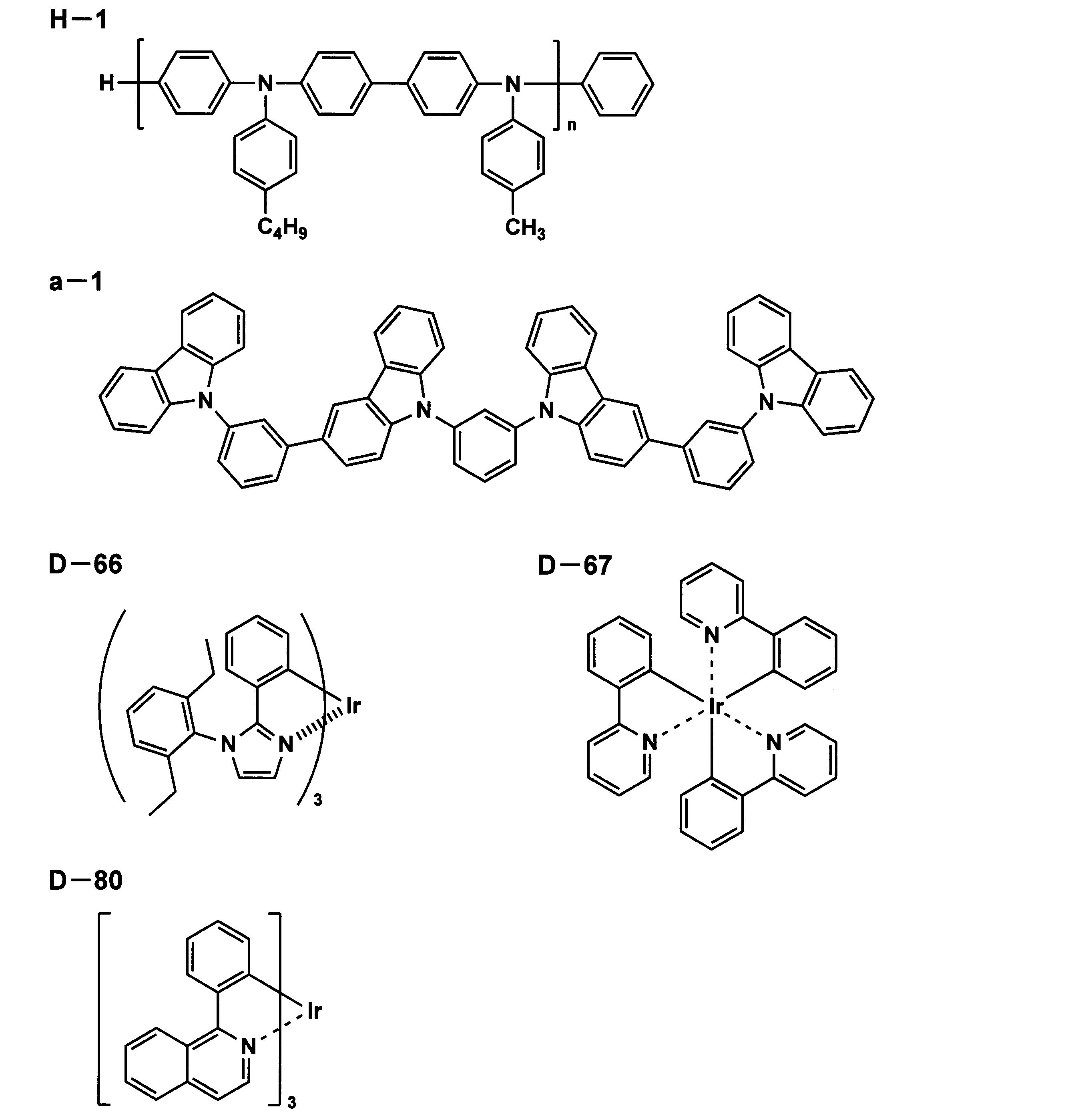
化合物a-1 1.42質量部
化合物D-66 0.25質量部
化合物D-67 0.004質量部
化合物D-80 0.004質量部
トルエン(沸点111℃) 100質量部
(d)電子輸送層の形成
続いて、20mgの下記化合物Aを、4mlの1-ブタノール(沸点117℃)に溶解して調製した電子輸送層形成用塗布液を、発光層上にスリットダイコーター(前出)により塗布し、層厚30nmの電子輸送層を形成した。なお、塗布は、窒素ガス雰囲気下において行った。
続いて、20mgの下記化合物Aを、4mlの1-ブタノール(沸点117℃)に溶解して調製した電子輸送層形成用塗布液を、発光層上にスリットダイコーター(前出)により塗布し、層厚30nmの電子輸送層を形成した。なお、塗布は、窒素ガス雰囲気下において行った。
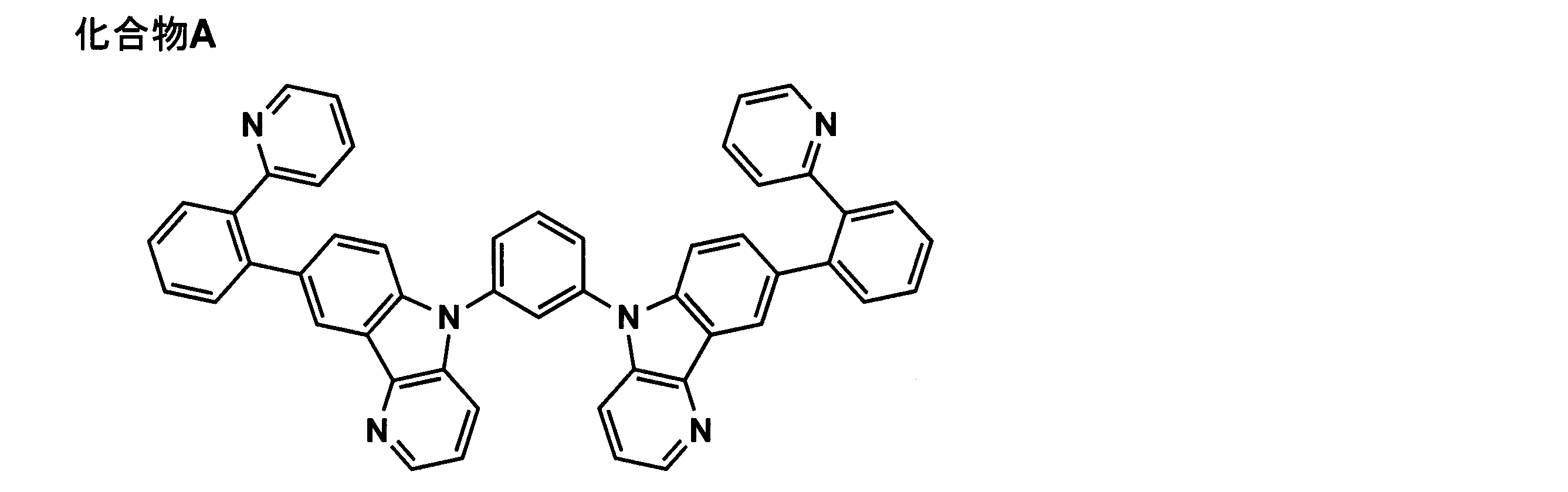
(e)加熱処理
上記のようにして電子輸送層まで形成した後、窒素ガス雰囲気下で、129℃で30分間保持して、加熱処理を行った。
上記のようにして電子輸送層まで形成した後、窒素ガス雰囲気下で、129℃で30分間保持して、加熱処理を行った。
(f)電子注入層及び陰極の形成
続いて、上記電子輸送層まで形成した樹脂基材を、大気に曝露することなく真空蒸着装置へ取り付けた。次いで、各モリブデン製抵抗加熱ボートにフッ化ナトリウム及びフッ化カリウムをそれぞれ入れたものを真空蒸着装置に取り付け、真空槽を4×10⁻⁵Paまで減圧した後、前記ボートを通電及び加熱して、フッ化ナトリウムを0.02nm/秒で前記電子輸送層上に層厚1nmの薄膜として形成し、続けて同様にフッ化カリウムを、0.02nm/秒でフッ化ナトリウム上に層厚1.5nmの薄膜として蒸着し、電子注入層を形成した。次いで、アルミニウムを厚さ100nmで蒸着して陰極を形成した。
続いて、上記電子輸送層まで形成した樹脂基材を、大気に曝露することなく真空蒸着装置へ取り付けた。次いで、各モリブデン製抵抗加熱ボートにフッ化ナトリウム及びフッ化カリウムをそれぞれ入れたものを真空蒸着装置に取り付け、真空槽を4×10⁻⁵Paまで減圧した後、前記ボートを通電及び加熱して、フッ化ナトリウムを0.02nm/秒で前記電子輸送層上に層厚1nmの薄膜として形成し、続けて同様にフッ化カリウムを、0.02nm/秒でフッ化ナトリウム上に層厚1.5nmの薄膜として蒸着し、電子注入層を形成した。次いで、アルミニウムを厚さ100nmで蒸着して陰極を形成した。
(封止)
引き続き、市販のローラーラミネート装置を用いて、封止部材を接着して、封止した。なお、封止部材としては、可撓性の厚さ30μmのアルミニウム箔(東洋アルミニウム株式会社製)に、ポリエチレンテレフタレート(PET)フィルム(12μm厚)をドライラミネーション用の接着剤(2液反応型のウレタン系接着剤)を用いてラミネートした(接着剤層の厚み1.5μm)ものを用いた。
引き続き、市販のローラーラミネート装置を用いて、封止部材を接着して、封止した。なお、封止部材としては、可撓性の厚さ30μmのアルミニウム箔(東洋アルミニウム株式会社製)に、ポリエチレンテレフタレート(PET)フィルム(12μm厚)をドライラミネーション用の接着剤(2液反応型のウレタン系接着剤)を用いてラミネートした(接着剤層の厚み1.5μm)ものを用いた。
アルミニウム面に封止用接着剤として、下記の熱硬化性接着剤を、ディスペンサを使用してアルミ箔の接着面(つや面)に沿って厚さ20μmで均一に塗布した。これを100Pa以下の真空下で12時間乾燥させた。さらに、露点温度が-80℃以下、酸素濃度0.8ppmの窒素雰囲気下へ移動し、12時間以上要して乾燥させ、封止用接着剤の含水率を100ppm以下となるように調整した。
熱硬化接着剤としては、下記の構成材料(A)~(C)を混合したエポキシ系接着剤を用いた。
(A)ビスフェノールAジグリシジルエーテル
(B)ジシアンジアミド
(C)エポキシアダクト系硬化促進剤
以上のようにして、封止基板を、取り出し電極及び電極リードの接合部を覆うようにして密着・配置し、圧着ローラーを用いて、厚着条件として圧着ローラー温度が120℃、圧力が0.5MPa、装置速度が0.3m/minで密着封止して、有機EL素子101を作製した。
(B)ジシアンジアミド
(C)エポキシアダクト系硬化促進剤
以上のようにして、封止基板を、取り出し電極及び電極リードの接合部を覆うようにして密着・配置し、圧着ローラーを用いて、厚着条件として圧着ローラー温度が120℃、圧力が0.5MPa、装置速度が0.3m/minで密着封止して、有機EL素子101を作製した。
〔有機EL素子102の作製〕
有機EL素子101の作製において、前記ガスバリアー層(A)の形成方法に代えて、下記のガスバリアー層(B)の形成方法に変更してガスバリアー層(B)を形成した以外は同様にして、有機EL素子102を作製した。
有機EL素子101の作製において、前記ガスバリアー層(A)の形成方法に代えて、下記のガスバリアー層(B)の形成方法に変更してガスバリアー層(B)を形成した以外は同様にして、有機EL素子102を作製した。
(ガスバリアー層(B)の形成)
シリコンターゲットを用い、酸素含有ガス雰囲気中で、有機EL素子101の作製に用いたのと同様の下地層を有するポリエチレンテレフタレートフィルム上に、反応スパッタ法により酸化ケイ素から構成されるガスバリアー層(B)を形成した。得られたガスバリアー層(B)の厚さは300nmであった。
シリコンターゲットを用い、酸素含有ガス雰囲気中で、有機EL素子101の作製に用いたのと同様の下地層を有するポリエチレンテレフタレートフィルム上に、反応スパッタ法により酸化ケイ素から構成されるガスバリアー層(B)を形成した。得られたガスバリアー層(B)の厚さは300nmであった。
得られたガスバリアー層(B)について、前記ガスバリアー層(A)について行ったXPSデプスプロファイル測定を同様にし、層厚方向の薄膜層の表面からの距離における、ケイ素分布曲線、酸素分布曲線、炭素分布曲線及び酸素炭素分布曲線を得た。得られたケイ素分布曲線、酸素分布曲線、炭素分布曲線及び酸素炭素分布曲線と、原子比とエッチング時間の関係とともに、原子比とガスバリアー層の表面からの距離(nm)との関係を併せて示すグラフを図4に示す。図4に示す結果からも明らかなように、得られた炭素分布曲線は極値を有しておらず、本発明で規定する条件(1)及び(2)からは外れるものであった。
〔有機EL素子103の作製〕
有機EL素子101の作製において、有機EL素子103を作製した。
有機EL素子101の作製において、有機EL素子103を作製した。
(ガスバリアー層(C)の形成)
特開平7-178860号公報の実施例3に記載されている成膜方法に従って、有機EL素子101の作製に用いたのと同様の下地層を有するポリエチレンテレフタレートフィルム上に、ガスバリアー層(C)を形成した。具体的には、蒸着源として、5mm程度の大きさの粒子状のSiO(純度99.7%)を用い、EB(Electron Beam)加熱蒸着法で、上記樹脂基材の下地層上に酸化ケイ素系(SiOx)ガスバリアー薄膜の形成を行った。フィルム送り速度を100m/min、印加電力5kWとし、厚さ300nmのガスバリアー層(C)を形成した。
特開平7-178860号公報の実施例3に記載されている成膜方法に従って、有機EL素子101の作製に用いたのと同様の下地層を有するポリエチレンテレフタレートフィルム上に、ガスバリアー層(C)を形成した。具体的には、蒸着源として、5mm程度の大きさの粒子状のSiO(純度99.7%)を用い、EB(Electron Beam)加熱蒸着法で、上記樹脂基材の下地層上に酸化ケイ素系(SiOx)ガスバリアー薄膜の形成を行った。フィルム送り速度を100m/min、印加電力5kWとし、厚さ300nmのガスバリアー層(C)を形成した。
次いで、反応ガスとして、プロピレンガスを用い、更に炭素置換を進めるためにチルローラー付近に設置した電極に高周波電圧を加え、プロピレンガスをプラズマ状態とした。流量を変化させるとともに励起用の電圧1kVを中心に振幅500Vで、sinカーブで変化させた。このようにして得られたガスバリアー層(C)について、炭素置換量と厚み方向の変化は、ESCA装置を用いて測定した。測定条件としては、Mg-Kα線を光源とし、出力8kV×30mA、真空度5×10⁻⁶Pa一定とした。
得られたガスバリアー層(C)の厚み方向の炭素分布の幅は1.0~2.8at%の範囲であり、最大の極値と最小の極値との差が5at%未満であり、本発明で規定する条件(2)からは外れるものであった。
〔有機EL素子104の作製〕
有機EL素子101の作製において、ガスバリアー層(A)を、下記の方法で形成するガスバリアー層(D)に変更した以外は同様にして、有機EL素子104を作製した。
有機EL素子101の作製において、ガスバリアー層(A)を、下記の方法で形成するガスバリアー層(D)に変更した以外は同様にして、有機EL素子104を作製した。
(ガスバリアー層(D)の形成)
特表2005-537963号公報に記載のガスバリアー層の形成方法であるPE-CVD(Plasma-Enhanced CVD)法を用いて、有機EL素子101の作製に用いたのと同様の下地層を有するポリエチレンテレフタレートフィルム上に、厚さ約300nmの傾斜組成のガスバリアー層(D)を形成した。
特表2005-537963号公報に記載のガスバリアー層の形成方法であるPE-CVD(Plasma-Enhanced CVD)法を用いて、有機EL素子101の作製に用いたのと同様の下地層を有するポリエチレンテレフタレートフィルム上に、厚さ約300nmの傾斜組成のガスバリアー層(D)を形成した。
シラン(最大流量約500sccm/min)、アンモニア(最大流量約60sccm/分)及びプロピレンオキシド(最大流量約500sccm/min)を用いて、ケイ素、炭素、酸素及び窒素からなる傾斜コーティングを作製した。反応体ガスの速度は蒸着中、コーティングの組成がその厚さ方向で連続的に変化するように変化させた。RF電極に供給した出力は、プラズマをプロピレンオキシドから発生させたときは100W、シランとアンモニアの混合物を反応器に供給したときは200Wとした。反応器内の真空レベルは26.6Paとし、平均温度は約55℃で行った。以上のようにして形成したガスバリアー層(D)の層厚方向におけるケイ素分布、酸素分布、炭素分布及び窒素分布を、前記ガスバリアー層(A)について行ったXPSデプスプロファイル測定と同様にして、ケイ素分布曲線、酸素分布曲線、炭素分布曲線及び窒素分布曲線を得た。
得られた分布曲線プロファイルを解析した結果、特表2005-537963号公報に記載されている図4と同様の元素分布プロファイルであり、炭素含有量が最大となる領域と、ケイ素含有量が最大値となる領域が交互に存在する元素プロファイルであり、ガスバリアー層におけるケイ素原子の比率が、本発明の条件(3)で規定する式(A)又は式(B)を満たす領域は、90%未満であった。
〔有機EL素子105の作製〕
上記有機EL素子104の作製において、電子輸送層を塗布形成した後、加熱処理条件として、窒素ガス雰囲気下で、105℃で30分間保持して、加熱処理を行った以外は同様にして、有機EL素子105を作製した。
上記有機EL素子104の作製において、電子輸送層を塗布形成した後、加熱処理条件として、窒素ガス雰囲気下で、105℃で30分間保持して、加熱処理を行った以外は同様にして、有機EL素子105を作製した。
〔有機EL素子106~110の作製〕
上記有機EL素子101の作製において、電子輸送層を塗布形成した後、加熱処理条件として、窒素ガス雰囲気下で、表1に記載の温度条件で30分間保持して、それぞれ加熱処理を施した以外は同様にして、有機EL素子106~110を作製した。
上記有機EL素子101の作製において、電子輸送層を塗布形成した後、加熱処理条件として、窒素ガス雰囲気下で、表1に記載の温度条件で30分間保持して、それぞれ加熱処理を施した以外は同様にして、有機EL素子106~110を作製した。
〔有機EL素子111~113の作製〕
上記有機EL素子101の作製において、正孔輸送層で用いる溶媒の種類と、電子輸送層を塗布形成した後の加熱処理条件を、表1に記載の条件に変更した以外は同様にして、有機EL素子111~113を作製した。
上記有機EL素子101の作製において、正孔輸送層で用いる溶媒の種類と、電子輸送層を塗布形成した後の加熱処理条件を、表1に記載の条件に変更した以外は同様にして、有機EL素子111~113を作製した。
〔有機EL素子114の作製〕
上記有機EL素子101の作製において、発光層の塗布液の調製に用いた溶媒を、トルエンからキシレン(沸点:144℃)に変更した以外は同様にして、有機EL素子114を作製した。
上記有機EL素子101の作製において、発光層の塗布液の調製に用いた溶媒を、トルエンからキシレン(沸点:144℃)に変更した以外は同様にして、有機EL素子114を作製した。
〔有機EL素子115の作製〕
上記有機EL素子111の作製において、樹脂基材を、PETから二軸延伸ポリエチレンナフタレートフィルム(PENフィルム、厚さ:125μm、幅:350mm、Tg:155℃)に変更し、かつ、電子輸送層を塗布形成した後、窒素ガス雰囲気下で、135℃で30分間の加熱処理を施した以外は同様にして、有機EL素子115を作製した。
上記有機EL素子111の作製において、樹脂基材を、PETから二軸延伸ポリエチレンナフタレートフィルム(PENフィルム、厚さ:125μm、幅:350mm、Tg:155℃)に変更し、かつ、電子輸送層を塗布形成した後、窒素ガス雰囲気下で、135℃で30分間の加熱処理を施した以外は同様にして、有機EL素子115を作製した。
〔有機EL素子116~118の作製〕
上記有機EL素子115の作製において、電子輸送層を塗布形成した後、加熱処理条件として、窒素ガス雰囲気下で、表1に記載の温度条件で30分間保持して、それぞれ加熱処理を施した以外は同様にして、有機EL素子116~118を作製した。
上記有機EL素子115の作製において、電子輸送層を塗布形成した後、加熱処理条件として、窒素ガス雰囲気下で、表1に記載の温度条件で30分間保持して、それぞれ加熱処理を施した以外は同様にして、有機EL素子116~118を作製した。
〔有機EL素子119の作製〕
上記有機EL素子118の作製において、発光層で用いる溶媒の種類と、電子輸送層を塗布形成した後の加熱処理条件を、表1に記載の条件に変更した以外は同様にして、有機EL素子119を作製した。
上記有機EL素子118の作製において、発光層で用いる溶媒の種類と、電子輸送層を塗布形成した後の加熱処理条件を、表1に記載の条件に変更した以外は同様にして、有機EL素子119を作製した。
〔有機EL素子120~122の作製〕
上記有機EL素子117の作製において、ガスバリアー層(A)を、それぞれガスバリアー層(B)~(D)に変更した以外は同様にして、有機EL素子120~122を作製した。
上記有機EL素子117の作製において、ガスバリアー層(A)を、それぞれガスバリアー層(B)~(D)に変更した以外は同様にして、有機EL素子120~122を作製した。
〔有機EL素子123及び124の作製〕
上記有機EL素子115の作製において、電子輸送層を塗布形成した後、加熱処理条件として、窒素ガス雰囲気下で、表1に記載の温度条件を30分間保持して、それぞれ加熱処理を施した以外は同様にして、有機EL素子123及び124を作製した。
上記有機EL素子115の作製において、電子輸送層を塗布形成した後、加熱処理条件として、窒素ガス雰囲気下で、表1に記載の温度条件を30分間保持して、それぞれ加熱処理を施した以外は同様にして、有機EL素子123及び124を作製した。

なお、表1に略称で記載した各構成要素の詳細は、以下のとおりである。
*A:PEDOT/PSS(ポリ(3,4-エチレンジオキシチオフェン)-ポリスチレンスルホネート)
溶媒1:クロロベンゼン(沸点:132℃)
溶媒2:トルエン(沸点:111℃)
溶媒3:キシレン(沸点:144℃)
溶媒4:n-BuOH(沸点:118℃)
溶媒5:酢酸n-ブチル(沸点:126℃)
溶媒6:酢酸イソプロピル(沸点:89℃)
溶媒7:塩化ヘキシル(沸点:134℃)
溶媒8:シクロヘキサン(沸点:155℃)
《有機EL素子の評価》
(発光効率の評価)
分光放射輝度計CS-2000(コニカミノルタ社製)を用いて、2.5mA/cm2定電流を印加したときの有機EL素子101~116の外部取り出し量子効率(%)を測定した。各測定結果を基に、有機EL素子101の外部取り出し量子効率(%)を100とする相対値で表示した。数値が大きいほど、すなわち、表2では100に近いほど、外部取り出し量子効率(%)である発光効率に優れていることを表す。
溶媒1:クロロベンゼン(沸点:132℃)
溶媒2:トルエン(沸点:111℃)
溶媒3:キシレン(沸点:144℃)
溶媒4:n-BuOH(沸点:118℃)
溶媒5:酢酸n-ブチル(沸点:126℃)
溶媒6:酢酸イソプロピル(沸点:89℃)
溶媒7:塩化ヘキシル(沸点:134℃)
溶媒8:シクロヘキサン(沸点:155℃)
《有機EL素子の評価》
(発光効率の評価)
分光放射輝度計CS-2000(コニカミノルタ社製)を用いて、2.5mA/cm2定電流を印加したときの有機EL素子101~116の外部取り出し量子効率(%)を測定した。各測定結果を基に、有機EL素子101の外部取り出し量子効率(%)を100とする相対値で表示した。数値が大きいほど、すなわち、表2では100に近いほど、外部取り出し量子効率(%)である発光効率に優れていることを表す。
(発光寿命の評価)
各有機EL素子について、23℃、50%RHの環境下で、10mA/cm2の定電流条件による連続発光を行い、分光放射輝度計CS-2000(コニカミノルタ社製)を用いて、初期輝度の半分の輝度になるのに要する時間(半減期:τ1/2)を測定した。なお、発光寿命の評価は、有機EL素子101の半減期(時間)を100とする相対値で表示した。数値が大きいほど、発光寿命が長いことを表す。
各有機EL素子について、23℃、50%RHの環境下で、10mA/cm2の定電流条件による連続発光を行い、分光放射輝度計CS-2000(コニカミノルタ社製)を用いて、初期輝度の半分の輝度になるのに要する時間(半減期:τ1/2)を測定した。なお、発光寿命の評価は、有機EL素子101の半減期(時間)を100とする相対値で表示した。数値が大きいほど、発光寿命が長いことを表す。
(耐久性の評価)
各有機EL素子に対し、85℃、85%RHの環境下で500時間の加熱処理を施した後、発光画像について、ダークスポットの発生の有無を目視確認し、下記の基準に従って耐久性を評価した。
各有機EL素子に対し、85℃、85%RHの環境下で500時間の加熱処理を施した後、発光画像について、ダークスポットの発生の有無を目視確認し、下記の基準に従って耐久性を評価した。
◎:ダークスポットの発生なく問題無し
○:ルーペで観察すると、微小サイズのダークスポットの発生が僅かに認められるが、目視では視認できないレベル
△:目視で、微小サイズのダークスポットの発生が僅かに認められる
×:目視で明らかに確認ができるダークスポットが発生している
以上により得られた各評価結果を、表2に示す。
○:ルーペで観察すると、微小サイズのダークスポットの発生が僅かに認められるが、目視では視認できないレベル
△:目視で、微小サイズのダークスポットの発生が僅かに認められる
×:目視で明らかに確認ができるダークスポットが発生している
以上により得られた各評価結果を、表2に示す。
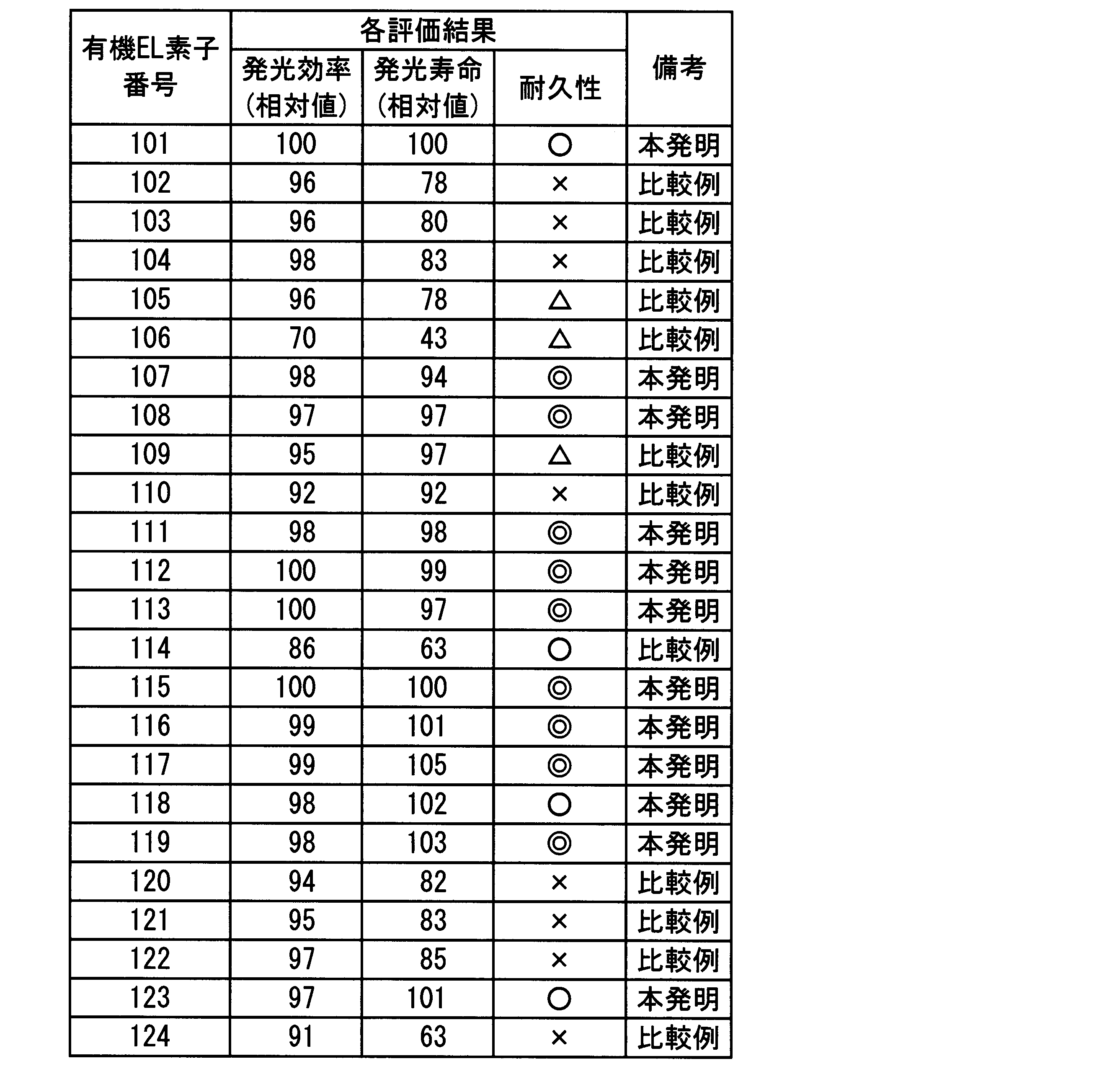
表2に記載の結果より明らかなように、ガスバリアー層の層厚方向におけるケイ素分布曲線、酸素分布曲線及び炭素分布曲線が、本発明で規定する条件(1)~(3)の全てを満たし、かつ、有機層を塗布した後の加熱条件を本発明で規定する条件(a)を満たす方法で作製した本発明の有機EL素子は、比較例に対し、高温高湿保存下でのダークスポットの発生が無く、発光効率及び発光寿命に優れていることが分かる。
実施例2
《有機EL素子の作製》
〔有機EL素子201~217の作製〕
実施例1に記載の有機EL素子101の作製において、ガスバリアー層の種類と、正孔注入層、正孔輸送層、発光層及び電子輸送層をそれぞれ塗布形成した後に、それぞれ独立して表3に記載の加熱処理条件で、逐次加熱処理を施した以外は同様にして、有機EL素子201~217を作製した。
《有機EL素子の作製》
〔有機EL素子201~217の作製〕
実施例1に記載の有機EL素子101の作製において、ガスバリアー層の種類と、正孔注入層、正孔輸送層、発光層及び電子輸送層をそれぞれ塗布形成した後に、それぞれ独立して表3に記載の加熱処理条件で、逐次加熱処理を施した以外は同様にして、有機EL素子201~217を作製した。
《有機EL素子の評価》
上記作製した有機EL素子201~217について、実施例1に記載の有機EL素子の各評価方法と同様にして、発光効率、発光寿命及び耐久性を評価した。
上記作製した有機EL素子201~217について、実施例1に記載の有機EL素子の各評価方法と同様にして、発光効率、発光寿命及び耐久性を評価した。
なお、発光効率及び発光寿命については、実施例1で作製した有機EL素子101の発光効率、発光寿命をそれぞれ100としたときの相対値で表示した。
以上により得られた結果を、表3に示す。

表3に記載の結果より明らかなように、本発明の構成条件であるガスバリアー層の層厚方向におけるケイ素分布曲線、酸素分布曲線及び炭素分布曲線が、本発明で規定する条件(1)~(3)の全てを満たし、かつ、本発明で規定する条件(b)を満たす方法で作製した本発明の有機EL素子は、比較例に対し、高温高湿保存下でのダークスポットの発生が無く、発光効率及び発光寿命に優れていることが分かる。
本発明の有機エレクトロルミネッセンス素子の製造方法により、透明樹脂フィルム基材を用い、経済性に優れ、ダークスポットの発生が抑制され、発光量子効率(発光輝度)及び発光寿命に優れたフレキシブルな有機エレクトロルミネッセンス素子を得ることができ、この有機エレクトロルミネッセンス素子は、表示デバイス、ディスプレイや、家庭用照明、車内照明、時計や液晶用のバックライト、看板広告、信号機、光記憶媒体の光源、電子写真複写機の光源、光通信処理機の光源、光センサーの光源、さらには表示装置を必要とする一般の家庭用電気器具等の広い発光光源として好適に利用できる。
1 透明樹脂フィルム基材
2 ガスバリアー層
3 第1電極(陽極)
4 有機層ユニット
5 第2電極(陰極)
6 封止部材
7 対向フィルム
11 送り出しローラー
21、22、23、24 搬送ローラー
31、32 成膜ローラー
41 ガス供給管
51 プラズマ発生用電源
61、62 磁場発生装置
71 巻取りローラー
A 炭素分布曲線
B ケイ素分布曲線
C 酸素分布曲線
D 酸素炭素分布曲線
F ガスバリアー性フィルム
EL 有機EL素子
2 ガスバリアー層
3 第1電極(陽極)
4 有機層ユニット
5 第2電極(陰極)
6 封止部材
7 対向フィルム
11 送り出しローラー
21、22、23、24 搬送ローラー
31、32 成膜ローラー
41 ガス供給管
51 プラズマ発生用電源
61、62 磁場発生装置
71 巻取りローラー
A 炭素分布曲線
B ケイ素分布曲線
C 酸素分布曲線
D 酸素炭素分布曲線
F ガスバリアー性フィルム
EL 有機EL素子
Claims (6)
- 透明樹脂フィルム基材上に、炭素原子、ケイ素原子及び酸素原子を含有するガスバリアー層と、陽極及び陰極と、当該陽極と陰極との間に、少なくとも発光層を含む複数の有機層で構成される有機層ユニットとを有する有機エレクトロルミネッセンス素子の製造方法であって、
前記ガスバリアー層は、X線光電子分光法による深さ方向の元素分布測定に基づき、当該ガスバリアー層の層厚方向における表面からの距離と、ケイ素原子、酸素原子及び炭素原子の合計量(100at%)に対する、ケイ素原子の量の比率(「ケイ素原子比率(at%)」という。)、酸素原子の量の比率(「酸素原子比率(at%)」という。)及び炭素原子の量の比率(「炭素原子比率(at%)」という。)との関係を示すケイ素分布曲線、酸素分布曲線及び炭素分布曲線が、下記条件(1)~(3)を満たし、
かつ、前記有機層ユニットは、各有機層の形成材料を溶媒に溶解して調製した各有機層塗布液を塗布することにより溶媒を含む有機層を形成した後、前記陰極を形成するまでの間の工程で、
下記式(a)で規定する加熱処理温度の範囲内で有機層を一括加熱処理して形成すること、
又は、下記式(b)で規定する加熱処理温度の範囲内で、各有機層を形成するごとに、逐次加熱処理して形成すること、
を特徴とする有機エレクトロルミネッセンス素子の製造方法。
(1)前記ガスバリアー層は、層厚方向で各原子の組成が連続的に変化し、かつ前記炭素分布曲線が極値を有する。
(2)前記炭素原子比率の最大の極値と最小の極値との差が、5at%以上である。
(3)前記ガスバリアー層の全層厚の90%以上の領域において、ケイ素原子、酸素原子及び炭素原子の合計量(100at%)に対する各原子の原子比率(at%)が、下記式(A)又は(B)で表される序列の大小関係を有する。
式(A):(炭素原子比率)<(ケイ素原子比率)<(酸素原子比率)
式(B):(酸素原子比率)<(ケイ素原子比率)<(炭素原子比率)
式(a):(有機層の形成に用いる溶媒のうち、最も高い沸点を有する溶媒の沸点-10℃)≦(加熱処理温度)≦(透明樹脂フィルム基材のガラス転移温度(Tg)+20℃)
式(b):(有機層形成用塗布液を構成する溶媒の沸点-10℃)≦(加熱処理温度)≦(透明樹脂フィルム基材のガラス転移温度(Tg)+20℃) - 前記式(a)で規定する加熱処理温度の範囲内で、前記有機層を一括加熱処理する工程が、最終の有機層を形成した後で、かつ前記陰極を形成する前の工程であることを特徴とする請求項1に記載の有機エレクトロルミネッセンス素子の製造方法。
- 前記有機層ユニットが、少なくとも正孔注入層、正孔輸送層、発光層及び電子輸送層で構成されることを特徴とする請求項1又は請求項2に記載の有機エレクトロルミネッセンス素子の製造方法。
- 前記発光層が、分子量2000以下の発光ホスト化合物と、分子量2000以下の発光ドーパントとを含有することを特徴とする請求項1から請求項3までのいずれか一項に記載の有機エレクトロルミネッセンス素子の製造方法。
- 前記ガスバリアー層を、有機ケイ素化合物を含む原料ガスと酸素ガスとを用い、対向する磁場を有する成膜ローラー間に放電空間を形成する放電プラズマ化学気相成長装置を用いて形成することを特徴とする請求項1から請求項4までのいずれか一項に記載の有機エレクトロルミネッセンス素子の製造方法。
- 前記透明樹脂フィルム基材が、二軸延伸されたポリエチレンテレフタレートフィルム又はポリエチレンナフタレートフィルムであることを特徴とする請求項1から請求項5までのいずれか一項に記載の有機エレクトロルミネッセンス素子の製造方法。
Priority Applications (1)
| Application Number | Priority Date | Filing Date | Title |
|---|---|---|---|
| JP2014551942A JPWO2014091868A1 (ja) | 2012-12-11 | 2013-11-15 | 有機エレクトロルミネッセンス素子の製造方法 |
Applications Claiming Priority (2)
| Application Number | Priority Date | Filing Date | Title |
|---|---|---|---|
| JP2012-269976 | 2012-12-11 | ||
| JP2012269976 | 2012-12-11 |
Publications (1)
| Publication Number | Publication Date |
|---|---|
| WO2014091868A1 true WO2014091868A1 (ja) | 2014-06-19 |
Family
ID=50934164
Family Applications (1)
| Application Number | Title | Priority Date | Filing Date |
|---|---|---|---|
| PCT/JP2013/080876 Ceased WO2014091868A1 (ja) | 2012-12-11 | 2013-11-15 | 有機エレクトロルミネッセンス素子の製造方法 |
Country Status (2)
| Country | Link |
|---|---|
| JP (1) | JPWO2014091868A1 (ja) |
| WO (1) | WO2014091868A1 (ja) |
Citations (5)
| Publication number | Priority date | Publication date | Assignee | Title |
|---|---|---|---|---|
| WO2008075625A1 (ja) * | 2006-12-18 | 2008-06-26 | Panasonic Corporation | 半導体デバイス |
| WO2010090087A1 (ja) * | 2009-02-03 | 2010-08-12 | コニカミノルタホールディングス株式会社 | 有機エレクトロニクス素子及びその製造方法 |
| JP2012081632A (ja) * | 2010-10-08 | 2012-04-26 | Sumitomo Chemical Co Ltd | 積層フィルム |
| JP2012081631A (ja) * | 2010-10-08 | 2012-04-26 | Sumitomo Chemical Co Ltd | 積層フィルム |
| JP2012128954A (ja) * | 2010-12-13 | 2012-07-05 | Konica Minolta Holdings Inc | 有機エレクトロルミネッセンス素子の製造方法および有機エレクトロルミネッセンス素子 |
-
2013
- 2013-11-15 WO PCT/JP2013/080876 patent/WO2014091868A1/ja not_active Ceased
- 2013-11-15 JP JP2014551942A patent/JPWO2014091868A1/ja active Pending
Patent Citations (5)
| Publication number | Priority date | Publication date | Assignee | Title |
|---|---|---|---|---|
| WO2008075625A1 (ja) * | 2006-12-18 | 2008-06-26 | Panasonic Corporation | 半導体デバイス |
| WO2010090087A1 (ja) * | 2009-02-03 | 2010-08-12 | コニカミノルタホールディングス株式会社 | 有機エレクトロニクス素子及びその製造方法 |
| JP2012081632A (ja) * | 2010-10-08 | 2012-04-26 | Sumitomo Chemical Co Ltd | 積層フィルム |
| JP2012081631A (ja) * | 2010-10-08 | 2012-04-26 | Sumitomo Chemical Co Ltd | 積層フィルム |
| JP2012128954A (ja) * | 2010-12-13 | 2012-07-05 | Konica Minolta Holdings Inc | 有機エレクトロルミネッセンス素子の製造方法および有機エレクトロルミネッセンス素子 |
Also Published As
| Publication number | Publication date |
|---|---|
| JPWO2014091868A1 (ja) | 2017-01-05 |
Similar Documents
| Publication | Publication Date | Title |
|---|---|---|
| JP6384326B2 (ja) | 有機エレクトロルミネッセンス素子 | |
| JP5470849B2 (ja) | 有機エレクトロルミネッセンス素子 | |
| JPWO2012121101A1 (ja) | 有機エレクトロルミネッセンス素子 | |
| JP2013200941A (ja) | 有機エレクトロルミネッセンス素子の製造方法 | |
| JP6939795B2 (ja) | 透明電極及び電子デバイス | |
| JP2008293680A (ja) | 有機エレクトロルミネッセンス素子及びその製造方法 | |
| JPWO2014188913A1 (ja) | 透明電極、及び、電子デバイス | |
| JP6390613B2 (ja) | 有機エレクトロルミネッセンス素子 | |
| WO2017056553A1 (ja) | 有機エレクトロルミネッセンス素子及びこれを備えた照明装置 | |
| JPWO2014199802A1 (ja) | 有機エレクトロルミネッセンス素子の製造方法 | |
| JP2009076241A (ja) | 有機エレクトロルミネッセンス素子の製造方法 | |
| JP5939249B2 (ja) | 有機エレクトロルミネッセンス素子の製造方法 | |
| JPWO2012077431A1 (ja) | 有機エレクトロルミネッセンス素子の製造方法 | |
| WO2013141190A1 (ja) | 有機エレクトロルミネッセンス素子用封止要素、有機エレクトロルミネッセンス素子の製造方法 | |
| JP5862663B2 (ja) | 有機エレクトロルミネッセンス素子の製造方法 | |
| JP5958464B2 (ja) | 有機エレクトロルミネッセンス素子およびその製造方法 | |
| US9818962B2 (en) | Organic electroluminescent element and method for manufacturing same | |
| JP2013074085A (ja) | 有機エレクトロルミネッセンス素子 | |
| JP5983618B2 (ja) | 有機エレクトロルミネッセンス素子の製造方法 | |
| JP6107825B2 (ja) | 有機エレクトロルミネッセンス素子 | |
| WO2014091868A1 (ja) | 有機エレクトロルミネッセンス素子の製造方法 | |
| JP2014103290A (ja) | 有機エレクトロルミネッセンス素子、有機エレクトロルミネッセンス素子の製造方法及び金属酸化物粒子含有組成物 | |
| JP5655640B2 (ja) | 有機エレクトロルミネッセンス素子および有機エレクトロルミネッセンス素子の製造方法 | |
| JPWO2014065213A1 (ja) | 透明電極、電子デバイス及び有機エレクトロルミネッセンス素子 | |
| WO2016174950A1 (ja) | 有機エレクトロルミネッセンス素子 |
Legal Events
| Date | Code | Title | Description |
|---|---|---|---|
| 121 | Ep: the epo has been informed by wipo that ep was designated in this application |
Ref document number: 13862371 Country of ref document: EP Kind code of ref document: A1 |
|
| ENP | Entry into the national phase |
Ref document number: 2014551942 Country of ref document: JP Kind code of ref document: A |
|
| NENP | Non-entry into the national phase |
Ref country code: DE |
|
| 122 | Ep: pct application non-entry in european phase |
Ref document number: 13862371 Country of ref document: EP Kind code of ref document: A1 |