WO2014088025A1 - パワーモジュール用基板、ヒートシンク付パワーモジュール用基板、パワーモジュール、パワーモジュール用基板の製造方法、銅板接合用ペースト、及び接合体の製造方法 - Google Patents
パワーモジュール用基板、ヒートシンク付パワーモジュール用基板、パワーモジュール、パワーモジュール用基板の製造方法、銅板接合用ペースト、及び接合体の製造方法 Download PDFInfo
- Publication number
- WO2014088025A1 WO2014088025A1 PCT/JP2013/082568 JP2013082568W WO2014088025A1 WO 2014088025 A1 WO2014088025 A1 WO 2014088025A1 JP 2013082568 W JP2013082568 W JP 2013082568W WO 2014088025 A1 WO2014088025 A1 WO 2014088025A1
- Authority
- WO
- WIPO (PCT)
- Prior art keywords
- copper plate
- ceramic substrate
- oxide
- substrate
- power module
- Prior art date
Links
Images


Classifications
-
- H—ELECTRICITY
- H05—ELECTRIC TECHNIQUES NOT OTHERWISE PROVIDED FOR
- H05K—PRINTED CIRCUITS; CASINGS OR CONSTRUCTIONAL DETAILS OF ELECTRIC APPARATUS; MANUFACTURE OF ASSEMBLAGES OF ELECTRICAL COMPONENTS
- H05K1/00—Printed circuits
- H05K1/02—Details
- H05K1/03—Use of materials for the substrate
- H05K1/0306—Inorganic insulating substrates, e.g. ceramic, glass
-
- B—PERFORMING OPERATIONS; TRANSPORTING
- B23—MACHINE TOOLS; METAL-WORKING NOT OTHERWISE PROVIDED FOR
- B23K—SOLDERING OR UNSOLDERING; WELDING; CLADDING OR PLATING BY SOLDERING OR WELDING; CUTTING BY APPLYING HEAT LOCALLY, e.g. FLAME CUTTING; WORKING BY LASER BEAM
- B23K1/00—Soldering, e.g. brazing, or unsoldering
- B23K1/0008—Soldering, e.g. brazing, or unsoldering specially adapted for particular articles or work
- B23K1/0016—Brazing of electronic components
-
- B—PERFORMING OPERATIONS; TRANSPORTING
- B23—MACHINE TOOLS; METAL-WORKING NOT OTHERWISE PROVIDED FOR
- B23K—SOLDERING OR UNSOLDERING; WELDING; CLADDING OR PLATING BY SOLDERING OR WELDING; CUTTING BY APPLYING HEAT LOCALLY, e.g. FLAME CUTTING; WORKING BY LASER BEAM
- B23K35/00—Rods, electrodes, materials, or media, for use in soldering, welding, or cutting
- B23K35/02—Rods, electrodes, materials, or media, for use in soldering, welding, or cutting characterised by mechanical features, e.g. shape
- B23K35/0222—Rods, electrodes, materials, or media, for use in soldering, welding, or cutting characterised by mechanical features, e.g. shape for use in soldering, brazing
- B23K35/0244—Powders, particles or spheres; Preforms made therefrom
- B23K35/025—Pastes, creams, slurries
-
- B—PERFORMING OPERATIONS; TRANSPORTING
- B23—MACHINE TOOLS; METAL-WORKING NOT OTHERWISE PROVIDED FOR
- B23K—SOLDERING OR UNSOLDERING; WELDING; CLADDING OR PLATING BY SOLDERING OR WELDING; CUTTING BY APPLYING HEAT LOCALLY, e.g. FLAME CUTTING; WORKING BY LASER BEAM
- B23K35/00—Rods, electrodes, materials, or media, for use in soldering, welding, or cutting
- B23K35/22—Rods, electrodes, materials, or media, for use in soldering, welding, or cutting characterised by the composition or nature of the material
- B23K35/24—Selection of soldering or welding materials proper
- B23K35/30—Selection of soldering or welding materials proper with the principal constituent melting at less than 1550 degrees C
- B23K35/3006—Ag as the principal constituent
-
- C—CHEMISTRY; METALLURGY
- C04—CEMENTS; CONCRETE; ARTIFICIAL STONE; CERAMICS; REFRACTORIES
- C04B—LIME, MAGNESIA; SLAG; CEMENTS; COMPOSITIONS THEREOF, e.g. MORTARS, CONCRETE OR LIKE BUILDING MATERIALS; ARTIFICIAL STONE; CERAMICS; REFRACTORIES; TREATMENT OF NATURAL STONE
- C04B35/00—Shaped ceramic products characterised by their composition; Ceramics compositions; Processing powders of inorganic compounds preparatory to the manufacturing of ceramic products
- C04B35/622—Forming processes; Processing powders of inorganic compounds preparatory to the manufacturing of ceramic products
- C04B35/64—Burning or sintering processes
- C04B35/645—Pressure sintering
-
- C—CHEMISTRY; METALLURGY
- C04—CEMENTS; CONCRETE; ARTIFICIAL STONE; CERAMICS; REFRACTORIES
- C04B—LIME, MAGNESIA; SLAG; CEMENTS; COMPOSITIONS THEREOF, e.g. MORTARS, CONCRETE OR LIKE BUILDING MATERIALS; ARTIFICIAL STONE; CERAMICS; REFRACTORIES; TREATMENT OF NATURAL STONE
- C04B37/00—Joining burned ceramic articles with other burned ceramic articles or other articles by heating
- C04B37/02—Joining burned ceramic articles with other burned ceramic articles or other articles by heating with metallic articles
- C04B37/023—Joining burned ceramic articles with other burned ceramic articles or other articles by heating with metallic articles characterised by the interlayer used
- C04B37/026—Joining burned ceramic articles with other burned ceramic articles or other articles by heating with metallic articles characterised by the interlayer used consisting of metals or metal salts
-
- H—ELECTRICITY
- H01—ELECTRIC ELEMENTS
- H01L—SEMICONDUCTOR DEVICES NOT COVERED BY CLASS H10
- H01L21/00—Processes or apparatus adapted for the manufacture or treatment of semiconductor or solid state devices or of parts thereof
- H01L21/02—Manufacture or treatment of semiconductor devices or of parts thereof
- H01L21/04—Manufacture or treatment of semiconductor devices or of parts thereof the devices having at least one potential-jump barrier or surface barrier, e.g. PN junction, depletion layer or carrier concentration layer
- H01L21/48—Manufacture or treatment of parts, e.g. containers, prior to assembly of the devices, using processes not provided for in a single one of the subgroups H01L21/06 - H01L21/326
- H01L21/4803—Insulating or insulated parts, e.g. mountings, containers, diamond heatsinks
- H01L21/4807—Ceramic parts
-
- H—ELECTRICITY
- H01—ELECTRIC ELEMENTS
- H01L—SEMICONDUCTOR DEVICES NOT COVERED BY CLASS H10
- H01L21/00—Processes or apparatus adapted for the manufacture or treatment of semiconductor or solid state devices or of parts thereof
- H01L21/02—Manufacture or treatment of semiconductor devices or of parts thereof
- H01L21/04—Manufacture or treatment of semiconductor devices or of parts thereof the devices having at least one potential-jump barrier or surface barrier, e.g. PN junction, depletion layer or carrier concentration layer
- H01L21/48—Manufacture or treatment of parts, e.g. containers, prior to assembly of the devices, using processes not provided for in a single one of the subgroups H01L21/06 - H01L21/326
- H01L21/4814—Conductive parts
- H01L21/4871—Bases, plates or heatsinks
- H01L21/4882—Assembly of heatsink parts
-
- H—ELECTRICITY
- H01—ELECTRIC ELEMENTS
- H01L—SEMICONDUCTOR DEVICES NOT COVERED BY CLASS H10
- H01L23/00—Details of semiconductor or other solid state devices
- H01L23/12—Mountings, e.g. non-detachable insulating substrates
- H01L23/14—Mountings, e.g. non-detachable insulating substrates characterised by the material or its electrical properties
- H01L23/15—Ceramic or glass substrates
-
- H—ELECTRICITY
- H01—ELECTRIC ELEMENTS
- H01L—SEMICONDUCTOR DEVICES NOT COVERED BY CLASS H10
- H01L23/00—Details of semiconductor or other solid state devices
- H01L23/34—Arrangements for cooling, heating, ventilating or temperature compensation ; Temperature sensing arrangements
- H01L23/36—Selection of materials, or shaping, to facilitate cooling or heating, e.g. heatsinks
- H01L23/367—Cooling facilitated by shape of device
- H01L23/3672—Foil-like cooling fins or heat sinks
-
- H—ELECTRICITY
- H01—ELECTRIC ELEMENTS
- H01L—SEMICONDUCTOR DEVICES NOT COVERED BY CLASS H10
- H01L23/00—Details of semiconductor or other solid state devices
- H01L23/34—Arrangements for cooling, heating, ventilating or temperature compensation ; Temperature sensing arrangements
- H01L23/36—Selection of materials, or shaping, to facilitate cooling or heating, e.g. heatsinks
- H01L23/373—Cooling facilitated by selection of materials for the device or materials for thermal expansion adaptation, e.g. carbon
- H01L23/3735—Laminates or multilayers, e.g. direct bond copper ceramic substrates
-
- H—ELECTRICITY
- H01—ELECTRIC ELEMENTS
- H01L—SEMICONDUCTOR DEVICES NOT COVERED BY CLASS H10
- H01L23/00—Details of semiconductor or other solid state devices
- H01L23/34—Arrangements for cooling, heating, ventilating or temperature compensation ; Temperature sensing arrangements
- H01L23/42—Fillings or auxiliary members in containers or encapsulations selected or arranged to facilitate heating or cooling
-
- H—ELECTRICITY
- H05—ELECTRIC TECHNIQUES NOT OTHERWISE PROVIDED FOR
- H05K—PRINTED CIRCUITS; CASINGS OR CONSTRUCTIONAL DETAILS OF ELECTRIC APPARATUS; MANUFACTURE OF ASSEMBLAGES OF ELECTRICAL COMPONENTS
- H05K1/00—Printed circuits
- H05K1/02—Details
- H05K1/0201—Thermal arrangements, e.g. for cooling, heating or preventing overheating
- H05K1/0203—Cooling of mounted components
- H05K1/021—Components thermally connected to metal substrates or heat-sinks by insert mounting
-
- H—ELECTRICITY
- H05—ELECTRIC TECHNIQUES NOT OTHERWISE PROVIDED FOR
- H05K—PRINTED CIRCUITS; CASINGS OR CONSTRUCTIONAL DETAILS OF ELECTRIC APPARATUS; MANUFACTURE OF ASSEMBLAGES OF ELECTRICAL COMPONENTS
- H05K1/00—Printed circuits
- H05K1/18—Printed circuits structurally associated with non-printed electric components
-
- H—ELECTRICITY
- H05—ELECTRIC TECHNIQUES NOT OTHERWISE PROVIDED FOR
- H05K—PRINTED CIRCUITS; CASINGS OR CONSTRUCTIONAL DETAILS OF ELECTRIC APPARATUS; MANUFACTURE OF ASSEMBLAGES OF ELECTRICAL COMPONENTS
- H05K3/00—Apparatus or processes for manufacturing printed circuits
- H05K3/0058—Laminating printed circuit boards onto other substrates, e.g. metallic substrates
- H05K3/0067—Laminating printed circuit boards onto other substrates, e.g. metallic substrates onto an inorganic, non-metallic substrate
-
- H—ELECTRICITY
- H05—ELECTRIC TECHNIQUES NOT OTHERWISE PROVIDED FOR
- H05K—PRINTED CIRCUITS; CASINGS OR CONSTRUCTIONAL DETAILS OF ELECTRIC APPARATUS; MANUFACTURE OF ASSEMBLAGES OF ELECTRICAL COMPONENTS
- H05K3/00—Apparatus or processes for manufacturing printed circuits
- H05K3/30—Assembling printed circuits with electric components, e.g. with resistor
- H05K3/303—Surface mounted components, e.g. affixing before soldering, aligning means, spacing means
-
- H—ELECTRICITY
- H05—ELECTRIC TECHNIQUES NOT OTHERWISE PROVIDED FOR
- H05K—PRINTED CIRCUITS; CASINGS OR CONSTRUCTIONAL DETAILS OF ELECTRIC APPARATUS; MANUFACTURE OF ASSEMBLAGES OF ELECTRICAL COMPONENTS
- H05K3/00—Apparatus or processes for manufacturing printed circuits
- H05K3/38—Improvement of the adhesion between the insulating substrate and the metal
- H05K3/388—Improvement of the adhesion between the insulating substrate and the metal by the use of a metallic or inorganic thin film adhesion layer
-
- C—CHEMISTRY; METALLURGY
- C04—CEMENTS; CONCRETE; ARTIFICIAL STONE; CERAMICS; REFRACTORIES
- C04B—LIME, MAGNESIA; SLAG; CEMENTS; COMPOSITIONS THEREOF, e.g. MORTARS, CONCRETE OR LIKE BUILDING MATERIALS; ARTIFICIAL STONE; CERAMICS; REFRACTORIES; TREATMENT OF NATURAL STONE
- C04B2235/00—Aspects relating to ceramic starting mixtures or sintered ceramic products
- C04B2235/65—Aspects relating to heat treatments of ceramic bodies such as green ceramics or pre-sintered ceramics, e.g. burning, sintering or melting processes
- C04B2235/656—Aspects relating to heat treatments of ceramic bodies such as green ceramics or pre-sintered ceramics, e.g. burning, sintering or melting processes characterised by specific heating conditions during heat treatment
- C04B2235/6565—Cooling rate
-
- C—CHEMISTRY; METALLURGY
- C04—CEMENTS; CONCRETE; ARTIFICIAL STONE; CERAMICS; REFRACTORIES
- C04B—LIME, MAGNESIA; SLAG; CEMENTS; COMPOSITIONS THEREOF, e.g. MORTARS, CONCRETE OR LIKE BUILDING MATERIALS; ARTIFICIAL STONE; CERAMICS; REFRACTORIES; TREATMENT OF NATURAL STONE
- C04B2237/00—Aspects relating to ceramic laminates or to joining of ceramic articles with other articles by heating
- C04B2237/02—Aspects relating to interlayers, e.g. used to join ceramic articles with other articles by heating
- C04B2237/12—Metallic interlayers
- C04B2237/121—Metallic interlayers based on aluminium
-
- C—CHEMISTRY; METALLURGY
- C04—CEMENTS; CONCRETE; ARTIFICIAL STONE; CERAMICS; REFRACTORIES
- C04B—LIME, MAGNESIA; SLAG; CEMENTS; COMPOSITIONS THEREOF, e.g. MORTARS, CONCRETE OR LIKE BUILDING MATERIALS; ARTIFICIAL STONE; CERAMICS; REFRACTORIES; TREATMENT OF NATURAL STONE
- C04B2237/00—Aspects relating to ceramic laminates or to joining of ceramic articles with other articles by heating
- C04B2237/02—Aspects relating to interlayers, e.g. used to join ceramic articles with other articles by heating
- C04B2237/12—Metallic interlayers
- C04B2237/122—Metallic interlayers based on refractory metals
-
- C—CHEMISTRY; METALLURGY
- C04—CEMENTS; CONCRETE; ARTIFICIAL STONE; CERAMICS; REFRACTORIES
- C04B—LIME, MAGNESIA; SLAG; CEMENTS; COMPOSITIONS THEREOF, e.g. MORTARS, CONCRETE OR LIKE BUILDING MATERIALS; ARTIFICIAL STONE; CERAMICS; REFRACTORIES; TREATMENT OF NATURAL STONE
- C04B2237/00—Aspects relating to ceramic laminates or to joining of ceramic articles with other articles by heating
- C04B2237/02—Aspects relating to interlayers, e.g. used to join ceramic articles with other articles by heating
- C04B2237/12—Metallic interlayers
- C04B2237/125—Metallic interlayers based on noble metals, e.g. silver
-
- C—CHEMISTRY; METALLURGY
- C04—CEMENTS; CONCRETE; ARTIFICIAL STONE; CERAMICS; REFRACTORIES
- C04B—LIME, MAGNESIA; SLAG; CEMENTS; COMPOSITIONS THEREOF, e.g. MORTARS, CONCRETE OR LIKE BUILDING MATERIALS; ARTIFICIAL STONE; CERAMICS; REFRACTORIES; TREATMENT OF NATURAL STONE
- C04B2237/00—Aspects relating to ceramic laminates or to joining of ceramic articles with other articles by heating
- C04B2237/02—Aspects relating to interlayers, e.g. used to join ceramic articles with other articles by heating
- C04B2237/12—Metallic interlayers
- C04B2237/126—Metallic interlayers wherein the active component for bonding is not the largest fraction of the interlayer
- C04B2237/127—The active component for bonding being a refractory metal
-
- C—CHEMISTRY; METALLURGY
- C04—CEMENTS; CONCRETE; ARTIFICIAL STONE; CERAMICS; REFRACTORIES
- C04B—LIME, MAGNESIA; SLAG; CEMENTS; COMPOSITIONS THEREOF, e.g. MORTARS, CONCRETE OR LIKE BUILDING MATERIALS; ARTIFICIAL STONE; CERAMICS; REFRACTORIES; TREATMENT OF NATURAL STONE
- C04B2237/00—Aspects relating to ceramic laminates or to joining of ceramic articles with other articles by heating
- C04B2237/02—Aspects relating to interlayers, e.g. used to join ceramic articles with other articles by heating
- C04B2237/12—Metallic interlayers
- C04B2237/126—Metallic interlayers wherein the active component for bonding is not the largest fraction of the interlayer
- C04B2237/128—The active component for bonding being silicon
-
- C—CHEMISTRY; METALLURGY
- C04—CEMENTS; CONCRETE; ARTIFICIAL STONE; CERAMICS; REFRACTORIES
- C04B—LIME, MAGNESIA; SLAG; CEMENTS; COMPOSITIONS THEREOF, e.g. MORTARS, CONCRETE OR LIKE BUILDING MATERIALS; ARTIFICIAL STONE; CERAMICS; REFRACTORIES; TREATMENT OF NATURAL STONE
- C04B2237/00—Aspects relating to ceramic laminates or to joining of ceramic articles with other articles by heating
- C04B2237/30—Composition of layers of ceramic laminates or of ceramic or metallic articles to be joined by heating, e.g. Si substrates
- C04B2237/32—Ceramic
- C04B2237/34—Oxidic
- C04B2237/343—Alumina or aluminates
-
- C—CHEMISTRY; METALLURGY
- C04—CEMENTS; CONCRETE; ARTIFICIAL STONE; CERAMICS; REFRACTORIES
- C04B—LIME, MAGNESIA; SLAG; CEMENTS; COMPOSITIONS THEREOF, e.g. MORTARS, CONCRETE OR LIKE BUILDING MATERIALS; ARTIFICIAL STONE; CERAMICS; REFRACTORIES; TREATMENT OF NATURAL STONE
- C04B2237/00—Aspects relating to ceramic laminates or to joining of ceramic articles with other articles by heating
- C04B2237/30—Composition of layers of ceramic laminates or of ceramic or metallic articles to be joined by heating, e.g. Si substrates
- C04B2237/40—Metallic
- C04B2237/402—Aluminium
-
- C—CHEMISTRY; METALLURGY
- C04—CEMENTS; CONCRETE; ARTIFICIAL STONE; CERAMICS; REFRACTORIES
- C04B—LIME, MAGNESIA; SLAG; CEMENTS; COMPOSITIONS THEREOF, e.g. MORTARS, CONCRETE OR LIKE BUILDING MATERIALS; ARTIFICIAL STONE; CERAMICS; REFRACTORIES; TREATMENT OF NATURAL STONE
- C04B2237/00—Aspects relating to ceramic laminates or to joining of ceramic articles with other articles by heating
- C04B2237/30—Composition of layers of ceramic laminates or of ceramic or metallic articles to be joined by heating, e.g. Si substrates
- C04B2237/40—Metallic
- C04B2237/407—Copper
-
- C—CHEMISTRY; METALLURGY
- C04—CEMENTS; CONCRETE; ARTIFICIAL STONE; CERAMICS; REFRACTORIES
- C04B—LIME, MAGNESIA; SLAG; CEMENTS; COMPOSITIONS THEREOF, e.g. MORTARS, CONCRETE OR LIKE BUILDING MATERIALS; ARTIFICIAL STONE; CERAMICS; REFRACTORIES; TREATMENT OF NATURAL STONE
- C04B2237/00—Aspects relating to ceramic laminates or to joining of ceramic articles with other articles by heating
- C04B2237/50—Processing aspects relating to ceramic laminates or to the joining of ceramic articles with other articles by heating
- C04B2237/60—Forming at the joining interface or in the joining layer specific reaction phases or zones, e.g. diffusion of reactive species from the interlayer to the substrate or from a substrate to the joining interface, carbide forming at the joining interface
-
- C—CHEMISTRY; METALLURGY
- C04—CEMENTS; CONCRETE; ARTIFICIAL STONE; CERAMICS; REFRACTORIES
- C04B—LIME, MAGNESIA; SLAG; CEMENTS; COMPOSITIONS THEREOF, e.g. MORTARS, CONCRETE OR LIKE BUILDING MATERIALS; ARTIFICIAL STONE; CERAMICS; REFRACTORIES; TREATMENT OF NATURAL STONE
- C04B2237/00—Aspects relating to ceramic laminates or to joining of ceramic articles with other articles by heating
- C04B2237/50—Processing aspects relating to ceramic laminates or to the joining of ceramic articles with other articles by heating
- C04B2237/70—Forming laminates or joined articles comprising layers of a specific, unusual thickness
- C04B2237/704—Forming laminates or joined articles comprising layers of a specific, unusual thickness of one or more of the ceramic layers or articles
-
- C—CHEMISTRY; METALLURGY
- C04—CEMENTS; CONCRETE; ARTIFICIAL STONE; CERAMICS; REFRACTORIES
- C04B—LIME, MAGNESIA; SLAG; CEMENTS; COMPOSITIONS THEREOF, e.g. MORTARS, CONCRETE OR LIKE BUILDING MATERIALS; ARTIFICIAL STONE; CERAMICS; REFRACTORIES; TREATMENT OF NATURAL STONE
- C04B2237/00—Aspects relating to ceramic laminates or to joining of ceramic articles with other articles by heating
- C04B2237/50—Processing aspects relating to ceramic laminates or to the joining of ceramic articles with other articles by heating
- C04B2237/70—Forming laminates or joined articles comprising layers of a specific, unusual thickness
- C04B2237/706—Forming laminates or joined articles comprising layers of a specific, unusual thickness of one or more of the metallic layers or articles
-
- C—CHEMISTRY; METALLURGY
- C04—CEMENTS; CONCRETE; ARTIFICIAL STONE; CERAMICS; REFRACTORIES
- C04B—LIME, MAGNESIA; SLAG; CEMENTS; COMPOSITIONS THEREOF, e.g. MORTARS, CONCRETE OR LIKE BUILDING MATERIALS; ARTIFICIAL STONE; CERAMICS; REFRACTORIES; TREATMENT OF NATURAL STONE
- C04B2237/00—Aspects relating to ceramic laminates or to joining of ceramic articles with other articles by heating
- C04B2237/50—Processing aspects relating to ceramic laminates or to the joining of ceramic articles with other articles by heating
- C04B2237/70—Forming laminates or joined articles comprising layers of a specific, unusual thickness
- C04B2237/708—Forming laminates or joined articles comprising layers of a specific, unusual thickness of one or more of the interlayers
-
- H—ELECTRICITY
- H01—ELECTRIC ELEMENTS
- H01L—SEMICONDUCTOR DEVICES NOT COVERED BY CLASS H10
- H01L2224/00—Indexing scheme for arrangements for connecting or disconnecting semiconductor or solid-state bodies and methods related thereto as covered by H01L24/00
- H01L2224/01—Means for bonding being attached to, or being formed on, the surface to be connected, e.g. chip-to-package, die-attach, "first-level" interconnects; Manufacturing methods related thereto
- H01L2224/26—Layer connectors, e.g. plate connectors, solder or adhesive layers; Manufacturing methods related thereto
- H01L2224/28—Structure, shape, material or disposition of the layer connectors prior to the connecting process
- H01L2224/29—Structure, shape, material or disposition of the layer connectors prior to the connecting process of an individual layer connector
- H01L2224/29001—Core members of the layer connector
- H01L2224/29099—Material
- H01L2224/291—Material with a principal constituent of the material being a metal or a metalloid, e.g. boron [B], silicon [Si], germanium [Ge], arsenic [As], antimony [Sb], tellurium [Te] and polonium [Po], and alloys thereof
- H01L2224/29101—Material with a principal constituent of the material being a metal or a metalloid, e.g. boron [B], silicon [Si], germanium [Ge], arsenic [As], antimony [Sb], tellurium [Te] and polonium [Po], and alloys thereof the principal constituent melting at a temperature of less than 400°C
- H01L2224/29111—Tin [Sn] as principal constituent
-
- H—ELECTRICITY
- H01—ELECTRIC ELEMENTS
- H01L—SEMICONDUCTOR DEVICES NOT COVERED BY CLASS H10
- H01L2224/00—Indexing scheme for arrangements for connecting or disconnecting semiconductor or solid-state bodies and methods related thereto as covered by H01L24/00
- H01L2224/01—Means for bonding being attached to, or being formed on, the surface to be connected, e.g. chip-to-package, die-attach, "first-level" interconnects; Manufacturing methods related thereto
- H01L2224/26—Layer connectors, e.g. plate connectors, solder or adhesive layers; Manufacturing methods related thereto
- H01L2224/31—Structure, shape, material or disposition of the layer connectors after the connecting process
- H01L2224/32—Structure, shape, material or disposition of the layer connectors after the connecting process of an individual layer connector
- H01L2224/321—Disposition
- H01L2224/32151—Disposition the layer connector connecting between a semiconductor or solid-state body and an item not being a semiconductor or solid-state body, e.g. chip-to-substrate, chip-to-passive
- H01L2224/32221—Disposition the layer connector connecting between a semiconductor or solid-state body and an item not being a semiconductor or solid-state body, e.g. chip-to-substrate, chip-to-passive the body and the item being stacked
- H01L2224/32225—Disposition the layer connector connecting between a semiconductor or solid-state body and an item not being a semiconductor or solid-state body, e.g. chip-to-substrate, chip-to-passive the body and the item being stacked the item being non-metallic, e.g. insulating substrate with or without metallisation
-
- H—ELECTRICITY
- H01—ELECTRIC ELEMENTS
- H01L—SEMICONDUCTOR DEVICES NOT COVERED BY CLASS H10
- H01L2224/00—Indexing scheme for arrangements for connecting or disconnecting semiconductor or solid-state bodies and methods related thereto as covered by H01L24/00
- H01L2224/80—Methods for connecting semiconductor or other solid state bodies using means for bonding being attached to, or being formed on, the surface to be connected
- H01L2224/83—Methods for connecting semiconductor or other solid state bodies using means for bonding being attached to, or being formed on, the surface to be connected using a layer connector
- H01L2224/8338—Bonding interfaces outside the semiconductor or solid-state body
- H01L2224/83399—Material
- H01L2224/834—Material with a principal constituent of the material being a metal or a metalloid, e.g. boron [B], silicon [Si], germanium [Ge], arsenic [As], antimony [Sb], tellurium [Te] and polonium [Po], and alloys thereof
- H01L2224/83438—Material with a principal constituent of the material being a metal or a metalloid, e.g. boron [B], silicon [Si], germanium [Ge], arsenic [As], antimony [Sb], tellurium [Te] and polonium [Po], and alloys thereof the principal constituent melting at a temperature of greater than or equal to 950°C and less than 1550°C
- H01L2224/83455—Nickel [Ni] as principal constituent
-
- H—ELECTRICITY
- H01—ELECTRIC ELEMENTS
- H01L—SEMICONDUCTOR DEVICES NOT COVERED BY CLASS H10
- H01L2224/00—Indexing scheme for arrangements for connecting or disconnecting semiconductor or solid-state bodies and methods related thereto as covered by H01L24/00
- H01L2224/80—Methods for connecting semiconductor or other solid state bodies using means for bonding being attached to, or being formed on, the surface to be connected
- H01L2224/83—Methods for connecting semiconductor or other solid state bodies using means for bonding being attached to, or being formed on, the surface to be connected using a layer connector
- H01L2224/838—Bonding techniques
- H01L2224/83801—Soldering or alloying
-
- H—ELECTRICITY
- H01—ELECTRIC ELEMENTS
- H01L—SEMICONDUCTOR DEVICES NOT COVERED BY CLASS H10
- H01L23/00—Details of semiconductor or other solid state devices
- H01L23/34—Arrangements for cooling, heating, ventilating or temperature compensation ; Temperature sensing arrangements
- H01L23/42—Fillings or auxiliary members in containers or encapsulations selected or arranged to facilitate heating or cooling
- H01L23/433—Auxiliary members in containers characterised by their shape, e.g. pistons
- H01L23/4336—Auxiliary members in containers characterised by their shape, e.g. pistons in combination with jet impingement
-
- H—ELECTRICITY
- H01—ELECTRIC ELEMENTS
- H01L—SEMICONDUCTOR DEVICES NOT COVERED BY CLASS H10
- H01L24/00—Arrangements for connecting or disconnecting semiconductor or solid-state bodies; Methods or apparatus related thereto
- H01L24/01—Means for bonding being attached to, or being formed on, the surface to be connected, e.g. chip-to-package, die-attach, "first-level" interconnects; Manufacturing methods related thereto
- H01L24/26—Layer connectors, e.g. plate connectors, solder or adhesive layers; Manufacturing methods related thereto
- H01L24/28—Structure, shape, material or disposition of the layer connectors prior to the connecting process
- H01L24/29—Structure, shape, material or disposition of the layer connectors prior to the connecting process of an individual layer connector
-
- H—ELECTRICITY
- H01—ELECTRIC ELEMENTS
- H01L—SEMICONDUCTOR DEVICES NOT COVERED BY CLASS H10
- H01L24/00—Arrangements for connecting or disconnecting semiconductor or solid-state bodies; Methods or apparatus related thereto
- H01L24/01—Means for bonding being attached to, or being formed on, the surface to be connected, e.g. chip-to-package, die-attach, "first-level" interconnects; Manufacturing methods related thereto
- H01L24/26—Layer connectors, e.g. plate connectors, solder or adhesive layers; Manufacturing methods related thereto
- H01L24/31—Structure, shape, material or disposition of the layer connectors after the connecting process
- H01L24/32—Structure, shape, material or disposition of the layer connectors after the connecting process of an individual layer connector
-
- H—ELECTRICITY
- H01—ELECTRIC ELEMENTS
- H01L—SEMICONDUCTOR DEVICES NOT COVERED BY CLASS H10
- H01L24/00—Arrangements for connecting or disconnecting semiconductor or solid-state bodies; Methods or apparatus related thereto
- H01L24/80—Methods for connecting semiconductor or other solid state bodies using means for bonding being attached to, or being formed on, the surface to be connected
- H01L24/83—Methods for connecting semiconductor or other solid state bodies using means for bonding being attached to, or being formed on, the surface to be connected using a layer connector
-
- H—ELECTRICITY
- H01—ELECTRIC ELEMENTS
- H01L—SEMICONDUCTOR DEVICES NOT COVERED BY CLASS H10
- H01L2924/00—Indexing scheme for arrangements or methods for connecting or disconnecting semiconductor or solid-state bodies as covered by H01L24/00
- H01L2924/013—Alloys
- H01L2924/0132—Binary Alloys
- H01L2924/01322—Eutectic Alloys, i.e. obtained by a liquid transforming into two solid phases
-
- H—ELECTRICITY
- H05—ELECTRIC TECHNIQUES NOT OTHERWISE PROVIDED FOR
- H05K—PRINTED CIRCUITS; CASINGS OR CONSTRUCTIONAL DETAILS OF ELECTRIC APPARATUS; MANUFACTURE OF ASSEMBLAGES OF ELECTRICAL COMPONENTS
- H05K2203/00—Indexing scheme relating to apparatus or processes for manufacturing printed circuits covered by H05K3/00
- H05K2203/04—Soldering or other types of metallurgic bonding
-
- H—ELECTRICITY
- H05—ELECTRIC TECHNIQUES NOT OTHERWISE PROVIDED FOR
- H05K—PRINTED CIRCUITS; CASINGS OR CONSTRUCTIONAL DETAILS OF ELECTRIC APPARATUS; MANUFACTURE OF ASSEMBLAGES OF ELECTRICAL COMPONENTS
- H05K2203/00—Indexing scheme relating to apparatus or processes for manufacturing printed circuits covered by H05K3/00
- H05K2203/11—Treatments characterised by their effect, e.g. heating, cooling, roughening
- H05K2203/1194—Thermal treatment leading to a different chemical state of a material, e.g. annealing for stress-relief, aging
Definitions
- the present invention relates to a power module substrate, a power module substrate with a heat sink, a power module, a method for manufacturing a power module substrate, a copper plate bonding paste, and a bonded body used in a semiconductor device that controls a large current and a high voltage. It is about the method.
- This application claims priority in Japanese Patent Application No. 2012-267300 for which it applied to Japan on December 06, 2012, and uses the content here.
- a power module for supplying power has a relatively high calorific value, and for example, AlN (aluminum nitride), Al 2 O 3 (alumina), Si 3 N 4 ( A ceramic substrate made of silicon nitride), a circuit layer formed by bonding a first metal plate to one surface side of the ceramic substrate, and a second metal plate bonded to the other surface side of the ceramic substrate.
- a power module substrate including a metal layer configured as described above is used.
- a semiconductor element such as a power element is mounted on a circuit layer via a solder material.
- Patent Document 1 proposes a power module substrate using an aluminum plate as a first metal plate (circuit layer) and a second metal plate (metal layer).
- the first metal plate (circuit layer) and the second metal plate (metal layer) are copper plates, and this copper plate is activated using an Ag—Cu—Ti brazing material.
- a power module substrate bonded to a ceramic substrate by a metal method.
- an aluminum plate is used as a first metal plate constituting the circuit layer.
- the thermal conductivity of aluminum is low. Therefore, when an aluminum plate is used as the circuit layer, an electrical component mounted on the circuit layer compared to the case where a copper plate is used. It is not possible to spread and dissipate heat from the heating element. For this reason, when the power density increases due to downsizing and high output of the electronic component, there is a possibility that heat cannot be sufficiently dissipated.
- Patent Documents 2 and 3 since the circuit layer is made of a copper plate, it is possible to efficiently dissipate heat from a heating element such as an electrical component mounted on the circuit layer. .
- a heating element such as an electrical component mounted on the circuit layer.
- an Ag—Cu—Ti brazing material is formed at the joint between the copper plate and the ceramic substrate.
- an Ag—Cu eutectic structure layer is formed.
- this Ag—Cu eutectic structure layer is very hard, when a cooling cycle was applied to the above power module substrate, shear stress due to the difference in thermal expansion coefficient between the ceramic substrate and the copper plate was applied. In some cases, the Ag-Cu eutectic structure layer is not deformed, and the ceramic substrate is cracked.
- the present invention has been made in view of the above-described circumstances, and is formed by bonding a copper plate made of copper or a copper alloy to a ceramic substrate made of Al 2 O 3 , and generation of cracks in the ceramic substrate at the time of a thermal cycle load. It is an object to provide a power module substrate, a power module substrate with a heat sink, a power module, and a method for manufacturing the power module substrate. Moreover, even when the copper plate and the ceramic substrate are joined, the hard Ag—Cu eutectic structure layer is not formed thick, and the occurrence of cracks in the ceramic substrate can be suppressed, and the copper plate and the ceramic substrate can be surely formed. It aims at providing the manufacturing method of the bonded body using the paste for copper plate joining which can join a board
- the power module substrate in one aspect of the present invention is a power module substrate in which a copper plate made of copper or a copper alloy is laminated and bonded to the surface of a ceramic substrate made of Al 2 O 3, and the copper plate An oxide layer is formed on the surface of the ceramic substrate and the thickness of the Ag—Cu eutectic structure layer is 15 ⁇ m or less.
- the thickness of the Ag—Cu eutectic structure layer is 15 ⁇ m or less at the joint between the copper plate made of copper or copper alloy and the ceramic substrate made of Al 2 O 3 . Even when a shear stress caused by the difference in thermal expansion coefficient between the ceramic substrate made of Al 2 O 3 and the copper plate is applied during a cold cycle, the copper plate side is appropriately deformed, and Al 2 O 3 Cracking of the ceramic substrate made of can be suppressed. Moreover, an oxide layer is formed on the surface of the ceramic substrate by reacting with oxygen contained in the ceramic substrate made of Al 2 O 3 , and the ceramic substrate and the oxide layer are firmly bonded. be able to.
- the power module substrate according to another aspect of the present invention is the power module substrate according to (1), wherein the oxide layer is selected from Ti, Hf, Zr, and Nb. Contains oxides of two or more elements. In this case, the ceramic substrate and the oxide layer are firmly bonded, and the ceramic substrate and the copper plate can be firmly bonded.
- a power module substrate with a heat sink includes the power module substrate according to (1) or (2) and a heat sink that cools the power module substrate.
- the heat generated in the power module substrate can be dissipated by the heat sink.
- the heat of the power module substrate can be reliably transmitted to the heat sink side.
- a power module according to another aspect of the present invention includes the power module substrate according to (1) or (2) and an electronic component mounted on the circuit layer. According to the power module of this configuration, the heat from the electronic components mounted on the circuit layer can be efficiently dissipated, and even when the power density (heat generation amount) of the electronic components is improved, it is sufficient It can correspond to.
- a method for manufacturing a power module substrate according to another aspect of the present invention is a method for manufacturing a power module substrate in which a copper plate made of copper or a copper alloy is laminated and bonded to the surface of a ceramic substrate made of Al 2 O 3.
- Forming step laminating step of laminating the ceramic substrate and the copper plate through the Ag and oxide forming element layer, pressurizing and heating the laminated ceramic substrate and the copper plate in the laminating direction, and the ceramic substrate And a heating step for forming a molten metal region at the interface between the copper plate and the copper plate, and solidifying the molten metal region, thereby Forming a molten metal region at the interface between the ceramic substrate and the copper plate by diffusing Ag to the copper plate side in the heating step.
- An oxide layer is formed on the surface of the ceramic substrate.
- the molten metal region is formed at the interface between the ceramic substrate and the copper plate by diffusing Ag to the copper plate side.
- the thickness of the molten metal region can be kept thin, and the thickness of the Ag—Cu eutectic structure layer can be made 15 ⁇ m or less.
- the oxide layer is formed on the surface of the ceramic substrate in the heating step, the ceramic substrate made of Al 2 O 3 and the copper plate can be firmly bonded.
- a method for manufacturing a power module substrate according to another aspect of the present invention is the method for manufacturing a power module substrate according to (5), wherein the oxide-forming elements are Ti, Hf, Zr, Nb. It is 1 type, or 2 or more types of elements selected from these.
- an oxide layer containing oxides of Ti, Hf, Zr, and Nb can be formed on the surface of the ceramic substrate, and the ceramic substrate made of Al 2 O 3 and the copper plate can be firmly bonded. It becomes possible.
- a method for manufacturing a power module substrate according to another aspect of the present invention is the method for manufacturing a power module substrate according to (5) or (6), wherein the Ag and oxide-forming element layer forming step is performed. Then, in addition to Ag and oxide forming elements, one or more additive elements selected from In, Sn, Al, Mn, and Zn are disposed. In this case, in the heating step, the molten metal region can be formed at a lower temperature, and the thickness of the Ag—Cu eutectic structure layer can be further reduced.
- a method for manufacturing a power module substrate according to another aspect of the present invention is the method for manufacturing a power module substrate according to any one of (5) to (7), wherein the Ag and the oxide forming element are used.
- the layer forming step Ag and an oxide-forming element layer-containing paste containing Ag and an oxide-forming element are applied.
- An element layer can be formed.
- a method for manufacturing a power module substrate according to another aspect of the present invention is the method for manufacturing a power module substrate according to (8), in which the Ag and the oxide-forming element layer-containing paste are oxidized. Contains hydrides of product-forming elements. In this case, since the hydrogen of the oxide forming element hydride acts as a reducing agent, the oxide film and the like formed on the surface of the copper plate can be removed, and the diffusion of Ag and the formation of the oxide layer can be reliably performed. .
- the copper plate bonding paste according to another aspect of the present invention is a copper plate bonding paste used when bonding a copper plate made of copper or a copper alloy and a ceramic substrate made of Al 2 O 3 , Ag And a powder component containing an oxide-forming element, a resin, and a solvent.
- the copper plate bonding paste of this configuration since it has a powder component containing Ag and an oxide forming element, when applied to the bonding portion between the copper plate and the ceramic substrate made of Al 2 O 3 and heated, When Ag in the powder component diffuses to the copper plate side, a molten metal region is formed by the reaction between Cu and Ag. The molten metal region is solidified to join the copper plate and the ceramic substrate made of Al 2 O 3 . That is, since the molten metal region is formed by diffusion of Ag into the copper plate, the molten metal region is not formed more than necessary at the joint, and the Ag—Cu eutectic structure layer formed after joining (after solidification). The thickness of the is reduced. As described above, since the hard Ag—Cu eutectic structure layer is formed thin, it is possible to suppress the occurrence of cracks in the ceramic substrate made of Al 2 O 3 .
- a copper plate bonding paste according to another aspect of the present invention is the copper plate bonding paste according to (10), wherein the powder component contains a hydride of the oxide-forming element.
- the powder component contains a hydride of the oxide-forming element.
- the hydrogen of the oxide forming element hydride acts as a reducing agent, the oxide film and the like formed on the surface of the copper plate can be removed, and the diffusion of Ag and the formation of the oxide layer can be reliably performed.
- a method for producing a joined body in another aspect of the present invention is a method for producing a joined body in which a copper plate made of copper or a copper alloy and a ceramic substrate made of Al 2 O 3 are joined, and the copper plate Heat treatment is performed with the copper plate bonding paste described in (10) or (11) interposed between the copper plate and the ceramic substrate to bond the copper plate and the ceramic substrate.
- the molten metal region can be formed by diffusing Ag contained in the copper plate bonding paste to the copper plate side. It is possible to join the copper plate and the ceramic substrate by solidifying the molten metal region. Therefore, since the hard Ag—Cu eutectic structure layer is formed thin, the occurrence of cracks in the ceramic substrate can be suppressed. Moreover, an oxide layer can be formed on the surface of the ceramic substrate, and the bonding strength between the copper plate and the ceramic substrate can be improved.
- a copper plate made of copper or a copper alloy is bonded to a ceramic substrate made of Al 2 O 3, and a power module substrate that can suppress the occurrence of cracks in the ceramic substrate during a thermal cycle load, a power with a heat sink
- a module substrate, a power module, and a method for manufacturing a power module substrate can be provided.
- FIG. 2 is an enlarged explanatory view of a bonding interface between a circuit layer and a ceramic substrate made of Al 2 O 3 in FIG.
- 1st embodiment of this invention it is a flowchart which shows the manufacturing method of the paste for copper plate joining containing Ag and an oxide formation element used when joining the copper plate used as a circuit layer, and a ceramic substrate.
- FIG. 8 is an enlarged explanatory view of a bonding interface between a circuit layer and a metal layer in FIG. 7 and a ceramic substrate.
- the ceramic substrate described in the embodiment of the present invention is a ceramic substrate made of Al 2 O 3 hereinafter.
- FIG. 1 shows a power module substrate 50 with a heat sink and a power module 1 using the power module substrate 10 according to this embodiment.
- the power module 1 includes a power module substrate 10 on which a circuit layer 12 is disposed, a semiconductor element 3 (electronic component) bonded to the surface of the circuit layer 12 via a solder layer 2, a buffer plate 41, And a heat sink 51.
- the solder layer 2 is made of, for example, a Sn—Ag, Sn—In, or Sn—Ag—Cu solder material.
- a Ni plating layer (not shown) is provided between the circuit layer 12 and the solder layer 2.
- the power module substrate 10 includes a ceramic substrate 11, a circuit layer 12 disposed on one surface of the ceramic substrate 11 (the first surface, the upper surface in FIG. 1), and the other surface of the ceramic substrate 11. And a metal layer 13 disposed on the second surface (the lower surface in FIG. 1).
- the ceramic substrate 11 prevents electrical connection between the circuit layer 12 and the metal layer 13, and is made of highly insulating Al 2 O 3 (alumina). Further, the thickness of the ceramic substrate 11 is set within a range of 0.2 to 1.5 mm, and in this embodiment is set to 0.635 mm.
- the circuit layer 12 is formed by bonding a copper plate 22 to the first surface (upper surface in FIG. 5) of the ceramic substrate 11.
- the thickness of the circuit layer 12 is set in a range of 0.1 mm or more and 1.0 mm or less, and is set to 0.3 mm in the present embodiment.
- a circuit pattern is formed on the circuit layer 12, and one surface (the upper surface in FIG. 1) is a mounting surface on which the semiconductor element 3 is mounted.
- the other surface (the lower surface in FIG. 1) of the circuit layer 12 is bonded to the first surface of the ceramic substrate 11.
- the copper plate 22 (circuit layer 12) is a rolled plate of oxygen-free copper (OFC) having a purity of 99.99% by mass or more.
- the copper plate may be a copper alloy rolled plate.
- a copper plate bonding paste containing Ag and an oxide forming element described later is used for bonding the ceramic substrate 11 and the circuit layer 12.
- the metal layer 13 is formed by bonding an aluminum plate 23 to the second surface (lower surface in FIG. 5) of the ceramic substrate 11.
- the thickness of the metal layer 13 is set within a range of 0.6 mm or more and 6.0 mm or less, and is set to 0.6 mm in the present embodiment.
- the aluminum plate 23 is a rolled plate of aluminum (so-called 4N aluminum) having a purity of 99.99% by mass or more.
- the buffer plate 41 absorbs strain generated by the cooling / heating cycle, and is formed on the other surface (the lower surface in FIG. 1) of the metal layer 13 as shown in FIG. One surface of the metal layer is bonded to the second surface of the ceramic substrate 11.
- the thickness of the buffer plate 41 is set in the range of 0.5 mm or more and 7.0 mm or less, and is set to 0.9 mm in this embodiment.
- the buffer plate 41 is a rolled plate of aluminum (so-called 4N aluminum) having a purity of 99.99% by mass or more.
- the heat sink 51 is for dissipating heat from the power module substrate 10 described above.
- the heat sink 51 in this embodiment is joined to the power module substrate 10 via the buffer plate 41.
- the heat sink 51 is made of aluminum and an aluminum alloy, and specifically, is a rolled plate of A6063 alloy. Further, the thickness of the heat sink 51 is set within a range of 1 mm or more and 10 mm or less, and is set to 5 mm in the present embodiment.
- FIG. 2 shows an enlarged view of the bonding interface between the ceramic substrate 11 and the circuit layer 12.
- an oxide layer 31 made of an oxide of an oxide forming element contained in the copper plate bonding paste is formed.
- An Ag—Cu eutectic structure layer 32 is formed so as to be laminated on the oxide layer 31.
- the thickness of the Ag—Cu eutectic structure layer 32 is 15 ⁇ m or less.
- a method for manufacturing the power module substrate 10 having the above-described configuration and a method for manufacturing the power module substrate 50 with a heat sink will be described.
- a copper plate bonding paste containing Ag and an oxide-forming element is used for bonding the ceramic substrate 11 and the copper plate 22 to be the circuit layer 12.
- the copper plate bonding paste will be described.
- the copper plate bonding paste contains a powder component containing Ag and an oxide-forming element, a resin, a solvent, a dispersant, a plasticizer, and a reducing agent.
- content of a powder component shall be 40 to 90 mass% of the whole copper plate bonding paste.
- the viscosity of the paste for copper plate bonding is adjusted to 10 Pa ⁇ s or more and 500 Pa ⁇ s or less, more preferably 50 Pa ⁇ s or more and 300 Pa ⁇ s or less.
- the oxide forming element is preferably one or more elements selected from Ti, Hf, Zr, and Nb.
- Ti is contained as the oxide forming element.
- the composition of the powder component is such that the content of the oxide forming element (Ti in the present embodiment) is 0.4 mass% or more and 75 mass% or less in order to apply the paste with an appropriate thickness, and the balance is Ag.
- 10% by mass of Ti is contained, and the balance is Ag and inevitable impurities.
- the alloy powder of Ag and Ti is used as a powder component containing Ag and an oxide formation element (Ti).
- This alloy powder is produced by an atomizing method, and the particle diameter is set to 40 ⁇ m or less, preferably 20 ⁇ m or less, more preferably 10 ⁇ m or less by sieving the produced alloy powder.
- the particle size of the alloy powder can be measured by using, for example, a microtrack method.
- the resin adjusts the viscosity of the copper plate bonding paste, and for example, ethyl cellulose, methyl cellulose, polymethyl methacrylate, acrylic resin, alkyd resin, and the like can be applied.
- the solvent is a solvent for the above-described powder component, and for example, methyl cellosolve, ethyl cellosolve, terpineol, toluene, texanol, triethyl citrate, etc. can be applied.
- the dispersant uniformly disperses the powder component, and for example, an anionic surfactant or a cationic surfactant can be applied.
- a plasticizer improves the moldability of the paste for copper plate joining, for example, dibutyl phthalate, dibutyl adipate, etc. are applicable.
- the reducing agent removes an oxide film or the like formed on the surface of the powder component. For example, rosin, abietic acid, or the like can be applied. In this embodiment, abietic acid is used.
- abietic acid is used.
- what is necessary is just to add a dispersing agent, a plasticizer, and a reducing agent as needed, and you may comprise the paste for copper plate joining, without adding a dispersing agent, a plasticizer, and a reducing agent.
- an alloy powder containing Ag and an oxide-forming element (Ti) is prepared by an atomizing method, and this is sieved to obtain an alloy powder having a particle size of 40 ⁇ m or less (alloy powder preparation step). S01). Moreover, a solvent and resin are mixed and an organic mixture is produced
- the preliminary mixture is mixed while kneading using a roll mill having a plurality of rolls (kneading step S04).
- the kneaded material obtained by kneading process S04 is filtered with a paste filter (filtration process S05). In this way, the above-described copper plate bonding paste is produced.
- Ag and the oxide-forming element layer 24 are formed on one surface of the ceramic substrate 11 by applying the above-described copper plate bonding paste by screen printing and drying.
- the thickness of Ag and the oxide formation element layer 24 shall be 60 micrometers or more and 300 micrometers or less after drying.
- the copper plate 22 and the ceramic substrate 11 are placed in a vacuum heating furnace while being pressurized in the stacking direction (pressure 1 to 35 kgf / cm 2 ) and heated. Then, as shown in FIG. 6, Ag and Ag in the oxide-forming element layer 24 diffuse toward the copper plate 22. At this time, a part of the copper plate 22 is melted by the reaction between Cu and Ag, and a molten metal region 27 is formed at the interface between the copper plate 22 and the ceramic substrate 11.
- the pressure in the vacuum heating furnace is set in the range of 10 ⁇ 6 Pa to 10 ⁇ 3 Pa, and the heating temperature is set in the range of 790 ° C. to 850 ° C.
- Method layer bonding step S15 Next, an aluminum plate 23 to be the metal layer 13 is bonded to the second surface side of the ceramic substrate 11.
- a brazing material foil 25 having an aluminum plate 23 to be a metal layer 13 having a thickness of 5 to 50 ⁇ m (14 ⁇ m in this embodiment) is provided on the second surface side of the ceramic substrate 11. Laminated.
- the brazing material foil 25 is an Al—Si based brazing material containing Si that is a melting point lowering element.
- the ceramic substrate 11 and the aluminum plate 23 are charged in a heating furnace in a state of being pressurized in the stacking direction (pressure 1 to 35 kgf / cm 2 ) and heated.
- the brazing filler metal foil 25 and a part of the aluminum plate 23 are melted, and a molten metal region is formed at the interface between the aluminum plate 23 and the ceramic substrate 11.
- the heating temperature is 550 ° C. or more and 650 ° C. or less
- the heating time is 30 minutes or more and 180 minutes or less.
- the ceramic substrate 11 and the aluminum plate 23 are joined by solidifying the molten metal region formed at the interface between the aluminum plate 23 and the ceramic substrate 11. In this way, the power module substrate 10 according to the present embodiment is produced.
- a buffer plate 41 and a heat sink 51 are placed on the other surface side (lower side in FIG. 5) of the metal layer 13 of the power module substrate 10. 52 are stacked. That is, the buffer plate 41 is laminated on the other surface of the metal layer 13 via the brazing material foil 42 so that one surface (the upper side in FIG. 5) of the buffer plate 41 faces the other surface of the metal layer 13. Furthermore, a heat sink 51 is laminated on the other surface (lower side in FIG. 5) of the buffer plate 41 via a brazing material foil 52.
- the brazing material foils 42 and 52 have a thickness of 5 to 50 ⁇ m (14 ⁇ m in this embodiment), and are Al—Si based brazing materials containing Si which is a melting point lowering element.
- the power module substrate 10, the buffer plate 41, and the heat sink 51 are charged in the stacking direction (pressure 1 to 35 kgf / cm 2 ) in a heating furnace and heated.
- molten metal regions are formed at the interface between the metal layer 13 and the buffer plate 41 and at the interface between the buffer plate 41 and the heat sink 51, respectively.
- the heating temperature is 550 ° C. or more and 650 ° C. or less
- the heating time is 30 minutes or more and 180 minutes or less.
- the power module substrate 10, the buffer plate 41, and the heat sink 51 are solidified by solidifying the molten metal regions respectively formed at the interface between the metal layer 13 and the buffer plate 41 and the interface between the buffer plate 41 and the heat sink 51. Join. As a result, the power module substrate with heat sink 50 according to the present embodiment is produced.
- the semiconductor element 3 is placed on the surface of the circuit layer 12 via a solder material, and soldered in a reduction furnace. Thereby, the power module 1 in which the semiconductor element 3 is bonded onto the circuit layer 12 via the solder layer 2 is produced.
- the thickness of the Ag—Cu eutectic structure layer 32 at the joint between the circuit layer 12 made of the copper plate 22 and the ceramic substrate 11. Is 15 ⁇ m or less, the circuit layer 12 side is appropriately deformed even when shear stress is applied due to the difference in thermal expansion coefficient between the ceramic substrate 11 and the circuit layer 12 during a thermal cycle load. Thus, cracking of the ceramic substrate 11 can be suppressed.
- the oxide layer 31 is formed on the surface of the ceramic substrate 11, the ceramic substrate 11 and the circuit layer 12 can be reliably bonded.
- the ceramic substrate 11 is made of Al 2 O 3 , the surface of the ceramic substrate 11 is reacted with the oxide substrate and the ceramic substrate 11 contained in the copper plate bonding paste.
- the oxide layer 31 is formed, and the ceramic substrate 11 and the oxide layer 31 are firmly bonded.
- the oxide layer 31 contains an oxide of one or more elements selected from Ti, Hf, Zr, and Nb.
- the oxide layer 31 is specifically TiO. 2 is contained, the ceramic substrate 11 and the oxide layer 31 are firmly bonded, and the ceramic substrate 11 and the circuit layer 12 can be firmly bonded.
- the heat generated in the power module substrate 10 can be dissipated by the heat sink 51.
- the circuit layer 12 and the ceramic substrate 11 are securely bonded, heat generated from the semiconductor element 3 mounted on the mounting surface of the circuit layer 12 can be reliably transmitted to the heat sink 51 side.
- the temperature rise of the semiconductor element 3 can be suppressed. Therefore, even when the power density (heat generation amount) of the semiconductor element 3 is improved, it is possible to cope with it sufficiently.
- the buffer plate 41 is disposed between the power module substrate 10 and the heat sink 51, the power module substrate 10 and the heat sink are arranged. Strain due to the difference in thermal expansion coefficient from 51 can be absorbed by the deformation of the buffer plate 41.
- the Ag and oxide formation element layer formation process S11 has Ag and oxide formation element layer formation process S11, lamination
- the Ag and oxide forming element layer forming step S ⁇ b> 11 the Ag and oxide forming element layer 24 containing Ag and the oxide forming element is formed on the bonding surface of the ceramic substrate 11.
- the ceramic substrate 11 and the copper plate 22 are stacked via the Ag and oxide forming element layer 24.
- the laminated ceramic substrate 11 and the copper plate 22 are pressed and heated in the lamination direction to form a molten metal region 27 at the interface between the ceramic substrate 11 and the copper plate 22.
- the ceramic substrate 11 and the copper plate 22 are joined by solidifying the molten metal region 27.
- the heating step S13 since the molten metal region 27 is formed at the interface between the ceramic substrate 11 and the copper plate 22 by diffusing Ag to the copper plate 22 side, the thickness of the molten metal region 27 can be kept thin.
- the thickness of the Ag—Cu eutectic structure layer 32 can be 15 ⁇ m or less.
- the oxide layer 31 is formed on the surface of the ceramic substrate 11 in the heating step S13, the ceramic substrate 11 and the copper plate 22 can be firmly bonded.
- the composition of the powder component in the copper plate bonding paste used in this embodiment is such that the content of the oxide-forming element is 0.4 mass% or more and 75 mass% or less, and the balance is Ag and inevitable impurities. Therefore, the oxide layer 31 can be formed on the surface of the ceramic substrate 11. Thus, since the ceramic substrate 11 and the circuit layer 12 made of the copper plate 22 are bonded via the oxide layer 31, the bonding strength between the ceramic substrate 11 and the circuit layer 12 can be improved.
- the particle size of the powder constituting the powder component that is, the alloy powder containing Ag and the oxide forming element (Ti) is 40 ⁇ m or less, the copper plate bonding paste is thinned. It becomes possible to apply. Therefore, the thickness of the Ag—Cu eutectic structure layer 32 formed after bonding (after solidification) can be reduced.
- content of a powder component shall be 40 mass% or more and 90 mass% or less, Ag is spread
- region 27 is formed reliably, and the copper plate 22 and the ceramic substrate 11 are made. Can be joined.
- the content of the solvent is ensured by the content of the powder component described above, and the copper plate bonding paste can be reliably applied to the bonding surface of the ceramic substrate 11, and the Ag and oxide forming element layer 24 can be reliably formed. Can be formed.
- the copper plate bonding paste contains a dispersant as necessary, the powder component can be dispersed and Ag can be diffused uniformly.
- the oxide layer 31 can be formed uniformly.
- the copper plate bonding paste contains a plasticizer as necessary, the shape of the copper plate bonding paste can be formed relatively freely, and the bonding surface of the ceramic substrate 11 can be reliably formed. Can be applied.
- the copper plate bonding paste contains a reducing agent as necessary, the action of the reducing agent can remove the oxide film formed on the surface of the powder component, the diffusion of Ag and The oxide layer 31 can be reliably formed.
- FIG. 7 shows a power module substrate 110 according to this embodiment.
- the power module substrate 110 includes a ceramic substrate 111, a circuit layer 112 disposed on one surface of the ceramic substrate 111 (the first surface, the upper surface in FIG. 7), and the other of the ceramic substrate 111. And a metal layer 113 disposed on the surface (the second surface, which is the lower surface in FIG. 7).
- the ceramic substrate 111 prevents electrical connection between the circuit layer 112 and the metal layer 113, and is made of Al 2 O 3 (alumina) having high insulation. Further, the thickness of the ceramic substrate 111 is set within a range of 0.2 to 1.5 mm, and is set to 0.32 mm in the present embodiment.
- the circuit layer 112 is formed by bonding a copper plate 122 to the first surface (upper surface in FIG. 10) of the ceramic substrate 111.
- the thickness of the circuit layer 112 is set within a range of 0.1 mm or more and 1.0 mm or less, and is set to 0.6 mm in the present embodiment.
- a circuit pattern is formed on the circuit layer 112, and one surface (the upper surface in FIG. 7) is a mounting surface on which a semiconductor element is mounted.
- the other surface (the lower surface in FIG. 7) of the circuit layer 112 is bonded to the first surface of the ceramic substrate 111.
- the copper plate 122 (circuit layer 112) is a rolled plate of oxygen-free copper (OFC) having a purity of 99.99% by mass or more.
- the metal layer 113 is formed by bonding a copper plate 123 to the second surface (the lower surface in FIG. 10) of the ceramic substrate 111.
- the thickness of the metal layer 113 is set within a range of 0.1 mm or more and 1.0 mm or less, and is set to 0.6 mm in the present embodiment.
- the copper plate 123 (metal layer 113) is an oxygen-free copper (OFC) rolled plate having a purity of 99.99% by mass or more.
- a copper plate bonding paste containing Ag and an oxide-forming element described later is used for bonding the ceramic substrate 111 and the circuit layer 112 and bonding the ceramic substrate 111 and the metal layer 113.
- FIG. 8 shows an enlarged view of the bonding interface between the ceramic substrate 111 and the circuit layer 112 and the metal layer 113.
- an oxide layer 131 made of an oxide of an oxide forming element contained in the copper plate bonding paste is formed on the surface of the ceramic substrate 111.
- the Ag—Cu eutectic structure layer observed in the first embodiment is not clearly observed.
- a method for manufacturing the power module substrate 110 having the above-described configuration will be described.
- a copper plate bonding paste containing Ag and an oxide forming element is used for bonding the ceramic substrate 111 and the copper plate 122 to be the circuit layer 112 .
- the copper plate bonding paste will be described.
- the copper plate bonding paste used in the present embodiment contains a powder component containing Ag and an oxide-forming element, a resin, a solvent, a dispersant, a plasticizer, and a reducing agent.
- the powder component contains one or more additive elements selected from In, Sn, Al, Mn, and Zn in addition to Ag and oxide forming elements. , Sn is contained.
- content of a powder component shall be 40 to 90 mass% of the whole copper plate bonding paste.
- the viscosity of the paste for copper plate bonding is adjusted to 10 Pa ⁇ s or more and 500 Pa ⁇ s or less, more preferably 50 Pa ⁇ s or more and 300 Pa ⁇ s or less.
- the oxide forming element is preferably one or more elements selected from Ti, Hf, Zr, and Nb.
- Zr is contained as the oxide forming element.
- the composition of the powder component is such that the content of the oxide-forming element (Zr in this embodiment) is 0.4 mass% or more and 75 mass% or less, and is selected from In, Sn, Al, Mn, and Zn.
- the content of one or more additive elements (Sn in this embodiment) is 0% by mass or more and 50% by mass or less, and the balance is Ag and inevitable impurities. However, the content of Ag is 25% by mass or more.
- Zr: 40 mass%, Sn: 20 mass% is contained, and the balance is Ag and inevitable impurities.
- element powder (Ag powder, Zr powder, Sn powder) is used as a powder component.
- These Ag powder, Zr powder, and Sn powder are blended so that the entire powder component has the above-described composition.
- These Ag powder, Zr powder, and Sn powder each have a particle size set to 40 ⁇ m or less, preferably 20 ⁇ m or less, and more preferably 10 ⁇ m or less.
- the particle size of these Ag powder, Zr powder, and Sn powder can be measured by using, for example, a microtrack method.
- the same resin and solvent as those in the first embodiment are applied. Also in this embodiment, a dispersant, a plasticizer, and a reducing agent are added as necessary.
- the copper plate bonding paste used in this embodiment is manufactured according to the manufacturing method shown in the first embodiment. That is, it is manufactured in the same procedure as in the first embodiment except that Ag powder, Zr powder, and Sn powder are used instead of the alloy powder.
- the first and second surfaces of the ceramic substrate 111 are coated with the above-described paste for bonding a copper plate according to the present embodiment by screen printing, and Ag and an oxide-forming element layer. 124 and 125 are formed. Note that the thicknesses of the Ag and oxide-forming element layers 124 and 125 are set to 60 ⁇ m or more and 300 ⁇ m or less after drying.
- the copper plate 122 is laminated on the first surface side of the ceramic substrate 111. Further, the copper plate 123 is laminated on the second surface side of the ceramic substrate 111. That is, Ag and oxide forming element layers 124 and 125 are interposed between the ceramic substrate 111 and the copper plate 122 and between the ceramic substrate 111 and the copper plate 123.
- the pressure in the vacuum heating furnace is set in the range of 10 ⁇ 6 Pa to 10 ⁇ 3 Pa, and the heating temperature is set in the range of 790 ° C. to 850 ° C.
- the power module substrate 110 according to the present embodiment is produced.
- a semiconductor element is mounted on the circuit layer 112, and a heat sink is disposed on the other side of the metal layer 113.
- the thickness of the Ag—Cu eutectic structure layer at the joint between the circuit layer 112 made of the copper plate 122 and the ceramic substrate 111 is small.
- the Ag—Cu eutectic structure layer is so thin that it is no longer observed, the difference in the thermal expansion coefficient between the ceramic substrate 111 and the circuit layer 112 during the thermal cycle load. Even when the shear stress due to the above acts, the circuit layer 112 side is appropriately deformed, and cracking of the ceramic substrate 111 can be suppressed.
- the oxide layer 131 is formed on the surface of the ceramic substrate 111, the ceramic substrate 111 and the circuit layer 112 can be reliably bonded.
- the molten metal region is formed by diffusion of Ag into the copper plates 122 and 123, the molten metal region is not formed more than necessary at the joint portion between the ceramic substrate 111 and the copper plates 122 and 123.
- the thickness of the Ag—Cu eutectic structure layer formed later) is reduced. Therefore, generation
- the ceramic substrate 111 made of Al 2 O 3 reacts with Zr to form the oxide layer 131, and the ceramic substrate 111 And the copper plates 122 and 123 can be reliably bonded.
- the ceramic substrate 111 made of Al 2 O 3 reacts with Zr to form the oxide layer 131, and the ceramic substrate 111 And the copper plates 122 and 123 can be reliably bonded.
- one or more additive elements selected from In, Sn, Al, Mn, and Zn two or more kinds of additive elements
- the molten metal region can be formed at a lower temperature, and the thickness of the formed Ag—Cu eutectic structure layer can be further reduced.
- the present invention is not limited to this, and other oxide forming elements such as Hf and Nb may be used.
- powder components contained in the copper bonding paste may also include a hydride of the oxide-forming elements such as TiH 2, ZrH 2.
- the hydrogen of the oxide forming element hydride acts as a reducing agent, the oxide film and the like formed on the surface of the copper plate can be removed, and the diffusion of Ag and the formation of the oxide layer can be reliably performed.
- 2nd embodiment although demonstrated as what added Sn as an addition element, it is not limited to this, 1 type, or 2 or more types selected from In, Sn, Al, Mn, and Zn These additional elements may be used.
- the present invention is not limited to this, and the particle size is not limited.
- the particle size is not limited.
- a dispersing agent a plasticizer, and a reducing agent, it is not limited to this and does not need to contain these.
- These dispersants, plasticizers, and reducing agents may be added as necessary.
- the power module substrate and the power module substrate with heat sink of the present invention are limited to the power module substrate and power module substrate with heat sink manufactured by the manufacturing method shown in FIGS. Instead, it may be a power module substrate manufactured by another manufacturing method.
- a copper plate 222 to be the circuit layer 212 is bonded to the first surface of the ceramic substrate 211 via the Ag and oxide forming element layer 224, and the solder plate is bonded to the second surface of the ceramic substrate 211.
- the aluminum plate 223 to be the metal layer 213 is joined via the material foil 225 (the second surface of the ceramic substrate 211 and one surface of the aluminum plate 223 to be the metal layer 213 are joined via the brazing material foil 225.
- a heat sink 251 may be joined to the other surface of the aluminum plate 223 via a brazing material foil 252. In this way, the power module substrate with heat sink 250 including the power module substrate 210 and the heat sink 251 is manufactured.
- a copper plate 322 to be the circuit layer 312 is joined to the first surface of the ceramic substrate 311 via the Ag and oxide forming element layer 324, and the second surface of the ceramic substrate 311 is brazed.
- the aluminum plate 323 to be the metal layer 313 is bonded via the material foil 325 (the second surface of the ceramic substrate 311 and one surface of the aluminum plate 323 to be the metal layer 313 are bonded via the brazing material foil 325.
- the power module substrate 310 is manufactured.
- a heat sink 351 may be bonded to the other surface of the metal layer 313 via a brazing material foil 352.
- the power module substrate 350 with a heat sink including the power module substrate 310 and the heat sink 351 is manufactured.
- a copper plate 422 to be a circuit layer 412 is bonded to the first surface of the ceramic substrate 411 through the Ag and oxide forming element layer 424, and the solder plate is bonded to the second surface of the ceramic substrate 411.
- the aluminum plate 423 to be the metal layer 413 is bonded via the material foil 425 (the second surface of the ceramic substrate 411 and one surface of the aluminum plate 423 to be the metal layer 413 are bonded via the brazing material foil 425.
- a buffer plate 441 is joined to the other surface of the aluminum plate 423 via a brazing material foil 442 (the other surface of the aluminum plate 423 and one surface of the buffer plate 441 are connected via a brazing material foil 442).
- the heat sink 451 may be bonded to the other surface of the buffer plate 441 via the brazing material foil 452. In this way, the power module substrate 450 with a heat sink including the power module substrate 410, the buffer plate 441, and the heat sink 451 is manufactured.
- the power module substrate manufactured by the structure and the manufacturing method shown in FIG. 10 by bonding the ceramic substrate and the copper plate using the various pastes shown in Table 1, Table 2 and Table 3, FIG. 11 and FIG. A power module substrate with a heat sink manufactured by the structure and manufacturing method shown, and a power module substrate with a heat sink manufactured by the structure and manufacturing method shown in FIGS.
- a copper plate is bonded to the first surface and the second surface of the ceramic substrate made of Al 2 O 3 using the above-mentioned various pastes, and the circuit layer and the metal layer are the copper plate. It was set as the board
- the power module substrate with a heat sink shown in FIGS. 11 and 12 was formed into a circuit layer by bonding a copper plate to the first surface of a ceramic substrate made of Al 2 O 3 using the various pastes described above. Further, an aluminum plate was joined to the second surface of the ceramic substrate made of Al 2 O 3 via a brazing material to form a metal layer. That is, the second surface of the ceramic substrate and one surface of the metal layer were joined via the brazing material. Note that 4N aluminum having a purity of 99.99% by mass or more was used as the aluminum plate, and Al-7.5% by mass Si and a brazing material foil having a thickness of 20 ⁇ m were used as the brazing material.
- an aluminum plate made of A6063 as a heat sink was joined to the metal layer side of the power module substrate via a brazing material on the other surface side of the metal layer.
- a brazing material foil of Al-7.5 mass% Si and a thickness of 70 ⁇ m was used as the brazing material.
- the power module substrate with a heat sink shown in FIG. 5 and FIG. 13 was formed as a circuit layer by bonding a copper plate to the first surface of a ceramic substrate made of Al 2 O 3 using the various pastes described above. Further, an aluminum plate was joined to the second surface of the ceramic substrate made of Al 2 O 3 via a brazing material to form a metal layer. That is, the second surface of the ceramic substrate and one surface of the metal layer were joined via the brazing material. In addition, 4N aluminum having a purity of 99.99% by mass or more was used as the aluminum plate, and Al-7.5% by mass Si and a 14 ⁇ m thick brazing material foil were used as the brazing material.
- an aluminum plate made of 4N aluminum was joined to the other surface of the metal layer as a buffer plate via a brazing material. That is, the other surface of the metal layer and one surface of the buffer plate were joined via the brazing material.
- a brazing material foil of Al-7.5 mass% Si and a thickness of 100 ⁇ m was used as the brazing material.
- the aluminum plate which consists of A6063 as a heat sink was joined to the metal layer side of the board
- the bonding of the ceramic substrate made of Al 2 O 3 and the copper plate was performed under the conditions shown in Table 4, Table 5, and Table 6.
- the bonding conditions for brazing the ceramic substrate made of Al 2 O 3 and the aluminum plate were a vacuum atmosphere, a pressure of 12 kgf / cm 2 , a heating temperature of 650 ° C., and a heating time of 30 minutes.
- the joining conditions for brazing the aluminum plates were a vacuum atmosphere, a pressure of 6 kgf / cm 2 , a heating temperature of 610 ° C., and a heating time of 30 minutes.
- Tables 4, 5, and 6 show the sizes of the ceramic substrates made of Al 2 O 3 .
- the size of the copper plate was 37 mm ⁇ 37 mm ⁇ 0.3 mm.
- the size of the aluminum plate used as the metal layer was 37 mm ⁇ 37 mm ⁇ 2.1 mm in the case of the power module substrate with a heat sink, and 37 mm ⁇ 37 mm ⁇ 0.6 mm in the case of the power module substrate with the heat sink and the buffer plate.
- the size of the aluminum plate used as a heat sink was 50 mm ⁇ 60 mm ⁇ 5 mm.
- the size of the aluminum plate used as the buffer plate was 40 mm ⁇ 40 mm ⁇ 0.9 mm.
- Tables 4, 5, and 6 describe the structures and manufacturing methods of the power module substrate, the power module substrate with a heat sink, the heat sink, and the power module substrate with a buffer plate that are configured using the various pastes described above.
- the structure “DBC” is the power module substrate shown in FIG.
- the structure “H-1” is a power module substrate with a heat sink shown in FIG.
- the structure “H-2” is a power module substrate with a heat sink shown in FIG.
- the structure “B-1” is a power module substrate with a heat sink shown in FIG.
- the structure “B-2” is the power module substrate with a heat sink shown in FIG.
- the film thickness conversion amount (converted average film thickness) was measured as follows and shown in Table 7, Table 8, and Table 9.
- various pastes shown in Table 1, Table 2, and Table 3 were applied to the interface between the ceramic substrate made of Al 2 O 3 and the copper plate and dried.
- the film thickness conversion amount (converted average film thickness) of each element in various dried pastes was measured.
- the film thickness is an average value obtained by measuring the locations (9 points) shown in FIG. 14 three times for each of the applied pastes using a fluorescent X-ray film thickness meter (STF9400 manufactured by SII Nano Technology Co., Ltd.). did.
- a sample with a known film thickness is measured in advance to obtain the relationship between the fluorescent X-ray intensity and the concentration, and based on the result, the film thickness converted amount of each element from the fluorescent X-ray intensity measured in each sample. It was determined.
- Ceramic cracks were evaluated by checking the occurrence of cracks every time the cold cycle ( ⁇ 45 ° C. to 125 ° C.) was repeated 500 times, and the number of cracks confirmed.
- the joining rate after the thermal cycle load was calculated by the following formula using the power module substrate after 4000 cycles of the thermal cycle ( ⁇ 45 ° C. to 125 ° C.).
- Bonding rate (initial bonding area-peeling area) / initial bonding area
- the oxide layer was formed by confirming the presence of the oxide forming element at the interface of the ceramic substrate made of copper plate / Al 2 O 3 from the mapping of the oxide forming element by EPMA (electron beam microanalyzer). Those in which oxides could be confirmed by the above method were indicated as “Yes” in the table, and those that could not be confirmed were described as “None”.
- the thickness of the Ag—Cu eutectic structure layer is as follows: from a backscattered electron image by EPMA (electron beam microanalyzer) at the ceramic substrate interface made of copper plate / Al 2 O 3 in a field of view of 2000 times magnification (length 45 ⁇ m; width 60 ⁇ m).
- the area of the Ag—Cu eutectic structure layer continuously formed at the bonding interface was measured and divided by the width of the measurement field of view, and the average of the five fields was taken as the thickness of the Ag—Cu eutectic structure layer. .
- the area of the Ag—Cu eutectic structure layer was measured.
- a copper plate made of copper or a copper alloy is bonded to a ceramic substrate made of Al 2 O 3, and a power module substrate that can suppress the occurrence of cracks in the ceramic substrate during a thermal cycle load, a power with a heat sink
- a module substrate, a power module, and a method for manufacturing a power module substrate can be provided.
- Power module 3 Semiconductor element (electronic component) 10, 110, 210, 310, 410 Power module substrate 11, 111, 211, 311, 411 Ceramic substrate 12, 112, 212, 312, 412 Circuit layer 13, 113, 213, 313, 413 Metal layer 22, 122, 123, 222, 322, 422 Copper plate 23, 223, 323, 423 Aluminum plate 31, 131 Oxide layer 32 Ag-Cu eutectic structure layer 41, 441 Buffer plate 50, 250, 350, 450 Power module substrate 51 with heat sink 251 351 451 Heat sink
Abstract
Description
本願は、2012年12月06日に日本に出願された特願2012-267300号について優先権を主張し、その内容をここに援用する。
このようなパワーモジュール基板では、回路層の上に、はんだ材を介してパワー素子等の半導体素子が搭載される。
また、特許文献2、3には、第一の金属板(回路層)及び第二の金属板(金属層)を銅板とし、この銅板を、Ag-Cu-Ti系のろう材を用いた活性金属法によってセラミックス基板に接合してなるパワーモジュール用基板が提案されている。
ところで、特許文献2,3に記載されたように、銅板とセラミックス基板とを活性金属法によって接合した場合には、銅板とセラミックス基板との接合部に、Ag-Cu-Ti系のろう材が溶融して凝固することによってAg-Cu共晶組織層が形成されることになる。
また、Al2O3からなるセラミックス基板に含有された酸素と反応することで前記セラミックス基板の表面に酸化物層が形成されることになり、前記セラミックス基板と酸化物層とが強固に結合することができる。
この場合、前記セラミックス基板と前記酸化物層とが強固に結合することになり、セラミックス基板と銅板とを強固に接合することができる。
この構成のヒートシンク付パワーモジュール用基板によれば、パワーモジュール用基板で発生した熱をヒートシンクによって放散することができる。また、銅板とセラミックス基板とが確実に接合されているので、パワーモジュール用基板の熱をヒートシンク側へと確実に伝達することが可能となる。
この構成のパワーモジュールによれば、回路層上に搭載された電子部品からの熱を効率的に放散することができ、電子部品のパワー密度(発熱量)が向上した場合であっても、十分に対応することができる。
この場合、前記セラミックス基板の表面に、Ti、Hf、Zr、Nbの酸化物を含む酸化物層を形成することができ、Al2O3からなるセラミックス基板と銅板とを強固に接合することが可能となる。
この場合、前記加熱工程において、前記溶融金属領域をさらに低い温度で形成することができ、Ag-Cu共晶組織層の厚さをさらに薄くすることができる。
この場合、Ag及び酸化物形成元素を含有する酸化物形成元素層含有ペーストを塗布することで、前記セラミックス基板の接合面及び前記銅板の接合面のうち少なくとも一方に、確実にAg及び酸化物形成元素層を形成することが可能となる。
この場合、酸化物形成元素の水素化物の水素が還元剤として作用するので、銅板の表面に形成された酸化膜等を除去でき、Agの拡散及び酸化物層の形成を確実に行うことができる。
すなわち、Agの銅板への拡散によって溶融金属領域が形成されることから、接合部において溶融金属領域が必要以上に形成されなくなり、接合後(凝固後)に形成されるAg-Cu共晶組織層の厚さが薄くなるのである。このように、硬いAg-Cu共晶組織層の厚さが薄く形成されることから、Al2O3からなるセラミックス基板における割れの発生を抑制することができる。
この場合、酸化物形成元素の水素化物の水素が還元剤として作用するので、銅板の表面に形成された酸化膜等を除去でき、Agの拡散及び酸化物層の形成を確実に行うことができる。
また、前記セラミックス基板の表面に酸化物層を形成することができ、銅板と前記セラミックス基板との接合強度の向上を図ることができる。
まず、第一の実施形態について説明する。図1に、本実施形態であるパワーモジュール用基板10を用いたヒートシンク付パワーモジュール用基板50及びパワーモジュール1を示す。
このパワーモジュール1は、回路層12が配設されたパワーモジュール用基板10と、回路層12の表面にはんだ層2を介して接合された半導体素子3(電子部品)と、緩衝板41と、ヒートシンク51とを備えている。ここで、はんだ層2は、例えばSn-Ag系、Sn-In系、若しくはSn-Ag-Cu系のはんだ材とされている。なお、本実施形態では、回路層12とはんだ層2との間にNiめっき層(図示なし)が設けられている。
セラミックス基板11は、回路層12と金属層13との間の電気的接続を防止するものであって、絶縁性の高いAl2O3(アルミナ)で構成されている。また、セラミックス基板11の厚さは、0.2~1.5mmの範囲内に設定されており、本実施形態では、0.635mmに設定されている。
本実施形態においては、銅板22(回路層12)は、純度99.99質量%以上の無酸素銅(OFC)の圧延板とされている。なお、この銅板は銅合金の圧延板とされてもよい。
ここで、セラミックス基板11と回路層12との接合には、後述するAg及び酸化物形成元素を含有する銅板接合用ペーストが使用されている。
本実施形態においては、アルミニウム板23(金属層13)は、純度が99.99質量%以上のアルミニウム(いわゆる4Nアルミニウム)の圧延板とされている。
本実施形態においては、緩衝板41は、純度が99.99質量%以上のアルミニウム(いわゆる4Nアルミニウム)の圧延板とされている。
本実施形態においては、ヒートシンク51は、アルミニウム及びアルミニウム合金で構成されており、具体的にはA6063合金の圧延板とされている。また、ヒートシンク51の厚さは1mm以上10mm以下の範囲内に設定されており、本実施形態では、5mmに設定されている。
そして、この酸化物層31に積層するようにAg-Cu共晶組織層32が形成されている。ここで、Ag-Cu共晶組織層32の厚さは15μm以下とされている。
上述のように、セラミックス基板11と回路層12となる銅板22の接合には、Ag及び酸化物形成元素を含有する銅板接合用ペーストが使用されている。そこで、まず、銅板接合用ペーストについて説明する。
ここで、粉末成分の含有量が、銅板接合用ペースト全体の40質量%以上90質量%以下とされている。
また、本実施形態では、銅板接合用ペーストの粘度が10Pa・s以上500Pa・s以下、より好ましくは50Pa・s以上300Pa・s以下に調整されている。
ここで、粉末成分の組成は、ペーストを適度な厚みで塗布するため、酸化物形成元素(本実施形態ではTi)の含有量が0.4質量%以上75質量%以下とされ、残部がAg及び不可避不純物とされていることが望ましい。本実施形態では、Tiを10質量%含んでおり、残部がAg及び不可避不純物とされている。
なお、この合金粉末の粒径は、例えば、マイクロトラック法を用いることで測定することができる。
溶剤は、前述の粉末成分の溶媒となるものであり、例えば、メチルセルソルブ、エチルセルソルブ、テルピネオール、トルエン、テキサノ-ル、トリエチルシトレート等を適用できる。
可塑剤は、銅板接合用ペーストの成形性を向上させるものであり、例えば、フタル酸ジブチル、アジピン酸ジブチル等を適用することができる。
還元剤は、粉末成分の表面に形成された酸化皮膜等を除去するものであり、例えば、ロジン、アビエチン酸等を適用することができる。なお、本実施形態では、アビエチン酸を用いている。
なお、分散剤、可塑剤、還元剤は、必要に応じて添加すればよく、分散剤、可塑剤、還元剤を添加することなく銅板接合用ペーストを構成してもよい。
まず、前述のように、Agと酸化物形成元素(Ti)とを含有する合金粉末をアトマイズ法によって作製し、これを篩い分けすることによって粒径40μm以下の合金粉末を得る(合金粉末作製工程S01)。
また、溶剤と樹脂とを混合して有機混合物を生成する(有機物混合工程S02)。
そして、合金粉末作製工程S01で得られた合金粉末と、有機物混合工程S02で得られた有機混合物と、分散剤、可塑剤、還元剤等の副添加剤と、をミキサーによって予備混合する(予備混合工程S03)。
次いで、予備混合物を、複数のロールを有するロールミル機を用いて練り込みながら混合する(混錬工程S04)。
混錬工程S04によって得られた混錬物を、ペーストろ過機によってろ過する(ろ過工程S05)。
このようにして、上述の銅板接合用ペーストが製出されることになる。
まず、図5に示すように、セラミックス基板11の一方の面に、スクリーン印刷によって、前述の銅板接合用ペーストを塗布して乾燥させることにより、Ag及び酸化物形成元素層24を形成する。なお、Ag及び酸化物形成元素層24の厚さは、乾燥後で60μm以上300μm以下とされている。
次に、銅板22をセラミックス基板11の第一の面側に積層する。すなわち、セラミックス基板11と銅板22との間に、Ag及び酸化物形成元素層24を介在させている。
次いで、銅板22、セラミックス基板11を積層方向に加圧(圧力1~35kgf/cm2)した状態で真空加熱炉内に装入して加熱する。すると、図6に示すように、Ag及び酸化物形成元素層24のAgが銅板22に向けて拡散する。このとき、銅板22の一部がCuとAgとの反応によって溶融し、銅板22とセラミックス基板11との界面に、溶融金属領域27が形成されることになる。
ここで、本実施形態では、真空加熱炉内の圧力は10-6Pa以上10-3Pa以下の範囲内に、加熱温度は790℃以上850℃以下の範囲内に設定している。
次に、溶融金属領域27を凝固させることにより、セラミックス基板11と銅板22とを接合する。なお、凝固工程S14が終了した後では、Ag及び酸化物形成元素層24のAgが十分に拡散されており、セラミックス基板11と銅板22との接合界面にAg及び酸化物形成元素層24が残存することはない。溶融金属領域27は、真空加熱炉の加熱を止めて自然冷却などで冷却されることによって凝固される。
次に、セラミックス基板11の第二の面側に金属層13となるアルミニウム板23を接合する。本実施形態では、図5に示すように、セラミックス基板11の第二の面側に、金属層13となるアルミニウム板23が厚さ5~50μm(本実施形態では14μm)のろう材箔25を介して積層される。なお、本実施形態においては、ろう材箔25は、融点降下元素であるSiを含有したAl-Si系のろう材とされている。
次に、セラミックス基板11、アルミニウム板23を積層方向に加圧(圧力1~35kgf/cm2)した状態で加熱炉内に装入して加熱する。すると、ろう材箔25とアルミニウム板23の一部とが溶融し、アルミニウム板23とセラミックス基板11との界面に溶融金属領域が形成される。ここで、加熱温度は550℃以上650℃以下、加熱時間は30分以上180分以下とされている。
次に、アルミニウム板23とセラミックス基板11との界面に形成された溶融金属領域を凝固させることにより、セラミックス基板11とアルミニウム板23とを接合する。
このようにして、本実施形態であるパワーモジュール用基板10が製出される。
次に、図5に示すように、パワーモジュール用基板10の金属層13の他方の面側(図5において下側)に、緩衝板41と、ヒートシンク51と、を、それぞれろう材箔42,52を介して積層する。すなわち、金属層13の他方の面に緩衝板41の一方の面(図5において上側)が対向するように金属層13の他方の面に緩衝板41をろう材箔42を介して積層し、さらにその緩衝板41の他方の面(図5において下側)にヒートシンク51をろう材箔52を介して積層する。
本実施形態では、ろう材箔42,52は、厚さ5~50μm(本実施形態では14μm)とされ、融点降下元素であるSiを含有したAl-Si系のろう材とされている。
次に、パワーモジュール用基板10、緩衝板41、ヒートシンク51を積層方向に加圧(圧力1~35kgf/cm2)した状態で加熱炉内に装入して加熱する。すると、金属層13と緩衝板41との界面及び緩衝板41とヒートシンク51との界面に、それぞれ溶融金属領域が形成される。ここで、加熱温度は550℃以上650℃以下、加熱時間は30分以上180分以下とされている。
これにより、本実施形態であるヒートシンク付パワーモジュール用基板50が製出されることになる。
これにより、はんだ層2を介して半導体素子3が回路層12上に接合されたパワーモジュール1が製出されることになる。
また、セラミックス基板11の表面に酸化物層31が形成されているので、セラミックス基板11と回路層12とを確実に接合することができる。
さらに、酸化物層31が、Ti、Hf、Zr、Nbから選択される1種又は2種以上の元素の酸化物を含有しており、本実施形態では、具体的に酸化物層31がTiO2を含有しているので、セラミックス基板11と酸化物層31とが強固に結合することになり、セラミックス基板11と回路層12とを強固に接合することができる。
さらに、本実施形態では、銅板接合用ペーストは必要に応じて可塑剤を含有しているので、銅板接合用ペーストの形状を比較的自由に成形することができ、セラミックス基板11の接合面に確実に塗布することができる。
また、本実施形態では、銅板接合用ペーストは必要に応じて還元剤を含有しているので、還元剤の作用により、粉末成分の表面に形成された酸化皮膜等を除去でき、Agの拡散及び酸化物層31の形成を確実に行うことができる。
次に、第二の実施形態について説明する。図7に、本実施形態であるパワーモジュール用基板110を示す。
このパワーモジュール用基板110は、セラミックス基板111と、このセラミックス基板111の一方の面(第一の面であり、図7において上面)に配設された回路層112と、セラミックス基板111の他方の面(第二の面であり、図7において下面)に配設された金属層113と、を備えている。
セラミックス基板111は、回路層112と金属層113との間の電気的接続を防止するものであって、絶縁性の高いAl2O3(アルミナ)で構成されている。また、セラミックス基板111の厚さは、0.2~1.5mmの範囲内に設定されており、本実施形態では、0.32mmに設定されている。
本実施形態においては、銅板122(回路層112)は、純度99.99質量%以上の無酸素銅(OFC)の圧延板とされている。
本実施形態においては、銅板123(金属層113)は、純度99.99質量%以上の無酸素銅(OFC)の圧延板とされている。
また、本実施形態では、第一の実施形態で観察されたAg-Cu共晶組織層が明確に観察されない構成とされている。
上述のように、セラミックス基板111と回路層112となる銅板122との接合には、Ag及び酸化物形成元素を含有する銅板接合用ペーストが使用されている。そこで、まず、銅板接合用ペーストについて説明する。
そして、粉末成分は、Ag及び酸化物形成元素以外に、In、Sn、Al、Mn及びZnから選択される1種又は2種以上の添加元素を含有するものとされており、本実施形態では、Snを含有している。
また、本実施形態では、銅板接合用ペーストの粘度が10Pa・s以上500Pa・s以下、より好ましくは50Pa・s以上300Pa・s以下に調整されている。
ここで、粉末成分の組成は、酸化物形成元素(本実施形態ではZr)の含有量が0.4質量%以上75質量%以下とされ、In、Sn、Al、Mn及びZnから選択される1種又は2種以上の添加元素(本実施形態ではSn)の含有量が0質量%以上50質量%以下とされ、残部がAg及び不可避不純物とされている。ただし、Agの含有量は25質量%以上である。本実施形態では、Zr;40質量%、Sn;20質量%を含んでおり、残部がAg及び不可避不純物とされている。
これらのAg粉末、Zr粉末、Sn粉末は、それぞれ粒径を40μm以下、好ましくは20μm以下、さらに好ましくは10μm以下に設定している。
なお、これらのAg粉末、Zr粉末、Sn粉末の粒径は、例えば、マイクロトラック法を用いることで測定することができる。
また、本実施形態で用いられる銅板接合用ペーストは、第一の実施形態で示した製造方法に準じて製造されている。すなわち、合金粉末の代わりに、Ag粉末、Zr粉末、Sn粉末を用いた以外は、第一の実施形態と同様の手順で製造されているのである。
まず、図10に示すように、セラミックス基板111の第一の面及び第二の面に、スクリーン印刷によって、前述の本実施形態である銅板接合用ペーストを塗布し、Ag及び酸化物形成元素層124,125を形成する。なお、Ag及び酸化物形成元素層124,125の厚さは、乾燥後で60μm以上300μm以下とされている。
次に、銅板122をセラミックス基板111の第一の面側に積層する。また、銅板123をセラミックス基板111の第二の面側に積層する。すなわち、セラミックス基板111と銅板122、セラミックス基板111と銅板123との間に、Ag及び酸化物形成元素層124,125を介在させている。
次いで、銅板122、セラミックス基板111、銅板123を積層方向に加圧(圧力1~35kgf/cm2)した状態で真空加熱炉内に装入して加熱する。すると、Ag及び酸化物形成元素層124のAgが銅板122に向けて拡散するとともに、Ag及び酸化物形成元素層125のAgが銅板123に向けて拡散する。
ここで、本実施形態では、真空加熱炉内の圧力は10-6Pa以上10-3Pa以下の範囲内に、加熱温度は790℃以上850℃以下の範囲内に設定している。
次に、溶融金属領域を凝固させることにより、セラミックス基板111と銅板122、123とを接合する。なお、凝固工程S114が終了した後では、Ag及び酸化物形成元素層124,125のAgが十分に拡散されており、セラミックス基板111と銅板122、123との接合界面にAg及び酸化物形成元素層124、125が残存することはない。溶融金属領域は、真空加熱炉の加熱を止めて自然冷却などで冷却されることによって凝固される。
このパワーモジュール用基板110には、回路層112の上に半導体素子が搭載されるとともに、金属層113の他方側にヒートシンクが配設されることになる。
また、セラミックス基板111の表面に酸化物層131が形成されているので、セラミックス基板111と回路層112とを確実に接合することができる。
そして、本実施形態では、粉末成分として、Ag及び酸化物形成元素(本実施形態ではZr)以外に、In、Sn、Al、Mn及びZnから選択される1種又は2種以上の添加元素(本実施形態ではSn)を含有しているので、溶融金属領域をさらに低い温度で形成することができ、形成されるAg-Cu共晶組織層の厚さをさらに薄くすることが可能となる。
例えば、酸化物形成元素としてTi、Zrを用いたものとして説明したが、これに限定されることはなく、Hf,Nb等の他の酸化物形成元素であってもよい。
また、銅板接合用ペースト(Ag及び酸化物形成元素層含有ペースト)に含まれる粉末成分がTiH2、ZrH2等の酸化物形成元素の水素化物を含んでいてもよい。この場合、酸化物形成元素の水素化物の水素が還元剤として作用するので、銅板の表面に形成された酸化膜等を除去でき、Agの拡散及び酸化物層の形成を確実に行うことができる。
また、第二の実施形態において、添加元素としてSnを添加したものとして説明したが、これに限定されることはなく、In、Sn、Al、Mn及びZnから選択される1種又は2種以上の添加元素を用いてもよい。
また、分散剤、可塑剤、還元剤を含むものとして説明したが、これに限定されることはなく、これらを含んでいなくてもよい。これら分散剤、可塑剤、還元剤は、必要に応じて添加すればよい。
また、分散剤としてアニオン性界面活性剤を、可塑剤としてアジピン酸ジブチルを、還元剤としてアビエチン酸を用いた。
粉末成分以外の樹脂、溶剤、分散剤、可塑剤、還元剤の混合比率は、質量比で、樹脂:溶剤:分散剤:可塑剤:還元剤=7:70:3:5:15とした。
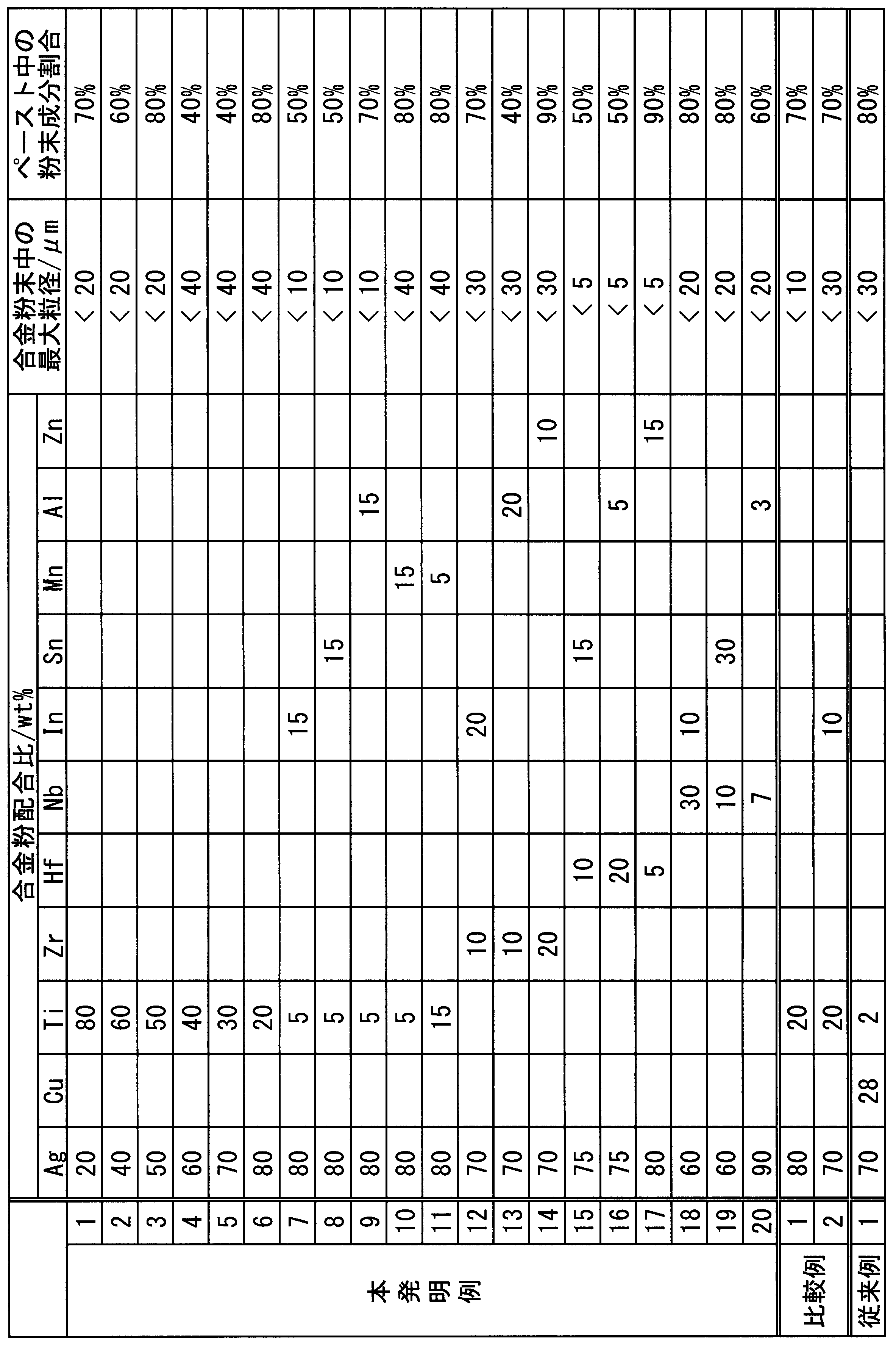


また、Al2O3からなるセラミックス基板の第二の面に、アルミニウム板をろう材を介して接合して金属層を形成した。すなわち、セラミックス基板の第二の面と金属層の一方の面とをろう材を介して接合した。なお、アルミニウム板として純度99.99質量%以上の4Nアルミを使用し、ろう材としてAl-7.5質量%Si、厚さ20μmのろう材箔を用いた。
さらに、金属層の他方の面側に、ヒートシンクとしてA6063からなるアルミニウム板を、ろう材を介してパワーモジュール用基板の金属層側に接合した。なお、ろう材としてAl-7.5質量%Si、厚さ70μmのろう材箔を用いた。
また、Al2O3からなるセラミックス基板の第二の面に、アルミニウム板をろう材を介して接合して金属層を形成した。すなわち、セラミックス基板の第二の面と金属層の一方の面とをろう材を介して接合した。なお、アルミニウム板として純度99.99質量%以上の4Nアルミニウムを使用し、ろう材としてAl-7.5質量%Si、厚さ14μmのろう材箔を用いた。
さらに、金属層の他方の面に、緩衝板として4Nアルミニウムからなるアルミニウム板をろう材を介して接合した。すなわち、金属層の他方の面と緩衝板の一方の面とをろう材を介して接合した。なお、ろう材としてAl-7.5質量%Si、厚さ100μmのろう材箔を用いた。
また、緩衝板の他方の面側に、ヒートシンクとしてA6063からなるアルミニウム板を、ろう材を介してパワーモジュール用基板の金属層側に接合した。なお、ろう材としてAl-7.5質量%Si、厚さ100μmのろう材箔を用いた。
また、Al2O3からなるセラミックス基板とアルミニウム板をろう付けする際の接合条件は、真空雰囲気、加圧圧力12kgf/cm2、加熱温度650℃、加熱時間30分とした。さらに、アルミニウム板同士をろう付けする際の接合条件は、真空雰囲気、加圧圧力6kgf/cm2、加熱温度610℃、加熱時間30分とした。
銅板のサイズは、37mm×37mm×0.3mmとした。
金属層となるアルミニウム板のサイズは、ヒートシンク付パワーモジュール用基板の場合は37mm×37mm×2.1mmとし、ヒートシンク及び緩衝板付パワーモジュール用基板の場合は37mm×37mm×0.6mmとした。
ヒートシンクとなるアルミニウム板のサイズは、50mm×60mm×5mmとした。
緩衝板となるアルミニウム板のサイズは、40mm×40mm×0.9mmとした。
構造「DBC」が図10に示すパワーモジュール用基板、
構造「H-1」が図11に示すヒートシンク付パワーモジュール用基板、
構造「H-2」が図12に示すヒートシンク付パワーモジュール用基板、
構造「B-1」が図13に示すヒートシンク付パワーモジュール用基板、
構造「B-2」が図5に示すヒートシンク付パワーモジュール用基板、である。
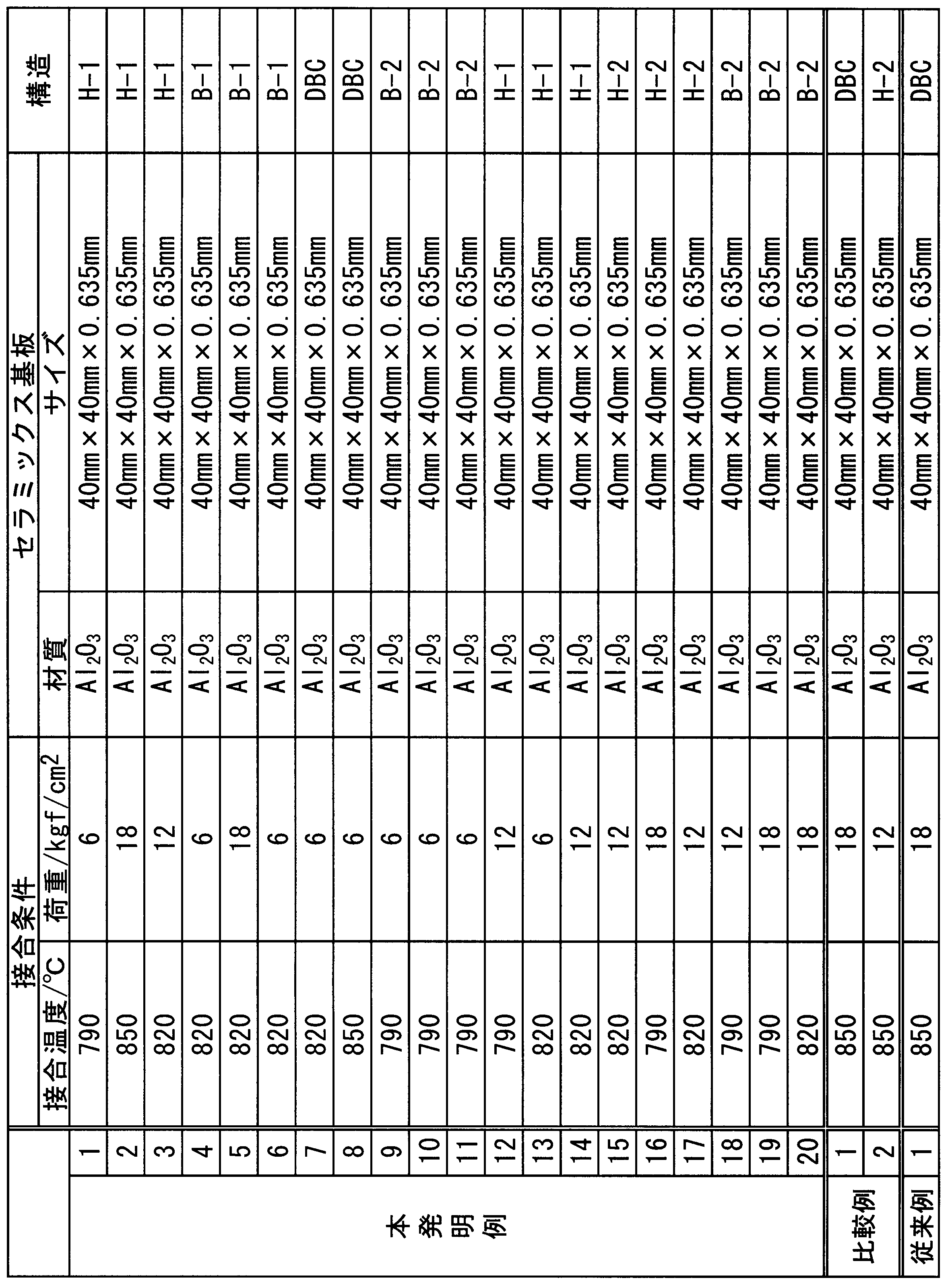


まず、Al2O3からなるセラミックス基板と銅板との界面に、表1、表2、表3に示す各種ペーストを塗布して乾燥した。乾燥された各種ペーストにおける各元素の膜厚換算量(換算平均膜厚)を測定した。
膜厚は、蛍光X線膜厚計(エスアイアイ・ナノテクノロジー株式会社製STF9400)を用いて、塗布した各種ペーストに対し、図14に示す箇所(9点)を各3回測定した平均値とした。なお、予め膜厚が既知のサンプルを測定して蛍光X線強度と濃度の関係を求めておき、その結果を基準として、各試料において測定された蛍光X線強度から各元素の膜厚換算量を決定した。
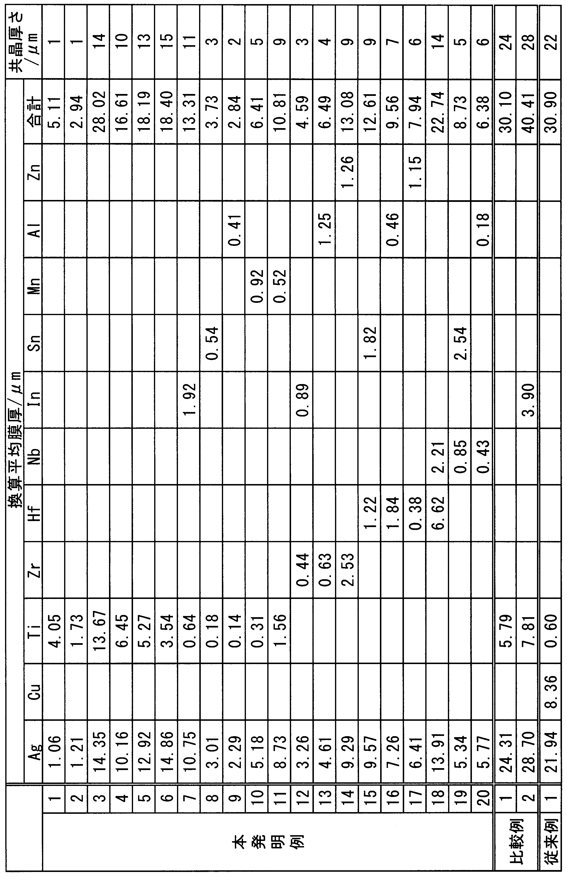


冷熱サイクル負荷後の接合率は、冷熱サイクル(-45℃から125℃)を4000回繰り返した後のパワーモジュール用基板を用いて、以下の式で算出した。なお、3500回を満たさないうちにクラックが発生した場合には、4000回繰り返した後の接合率については評価しなかった。
接合率 = (初期接合面積-剥離面積)/初期接合面積
Ag-Cu共晶組織層の厚さは、銅板/Al2O3からなるセラミックス基板界面のEPMA(電子線マイクロアナライザー)による反射電子像から、倍率2000倍の視野(縦45μm;横60μm)において接合界面に連続的に形成されたAg-Cu共晶組織層の面積を測定し、測定視野の幅の寸法で除して求め、5視野の平均をAg-Cu共晶組織層の厚さとした。なお、銅板とAl2O3からなるセラミックス基板との接合部に形成されたAg-Cu共晶組織層のうち、接合界面から厚さ方向に連続的に形成されていない領域を含めずに、Ag-Cu共晶組織層の面積を測定した。
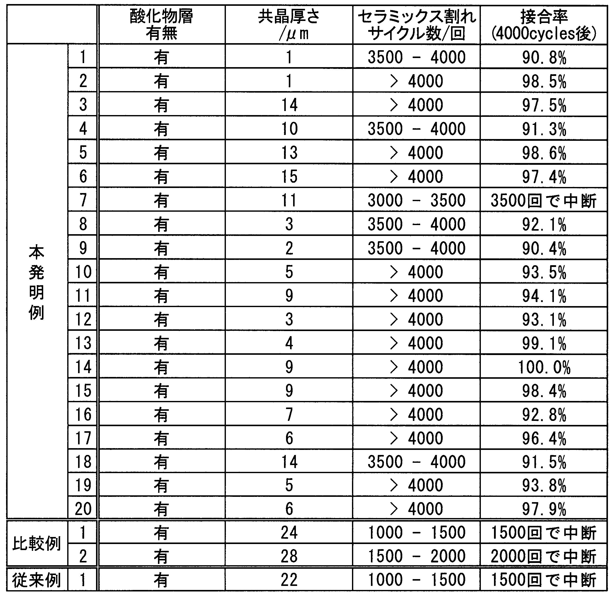


また、従来例1及び従来例51では、共晶組織厚さが15μmを超えており、比較例と同様に少ないサイクル数でAl2O3からなるセラミックス基板にクラックが発生した。
一方、共晶組織厚さが15μm以下とされた本発明例1-20、51-70、81-86においては、Al2O3からなるセラミックス基板におけるクラックの発生が抑制されていることが確認される。
以上の結果から、本発明例によれば、冷熱サイクル負荷時におけるAl2O3からなるセラミックス基板の割れの発生を抑制できるパワーモジュール用基板を提供できることが確認された。
10、110、210、310、410 パワーモジュール用基板
11、111、211、311、411 セラミックス基板
12、112、212、312、412 回路層
13、113、213、313、413 金属層
22、122、123、222、322、422 銅板
23、223、323、423 アルミニウム板
31、131 酸化物層
32 Ag-Cu共晶組織層
41、441 緩衝板
50、250、350、450 ヒートシンク付パワーモジュール用基板
51、251、351、451 ヒートシンク
Claims (13)
- Al2O3からなるセラミックス基板の表面に銅または銅合金からなる銅板が積層されて接合されたパワーモジュール用基板であって、
前記銅板と前記セラミックス基板との間において、前記セラミックス基板の表面に酸化物層が形成されているとともに、Ag-Cu共晶組織層の厚さが15μm以下とされていることを特徴とするパワーモジュール用基板。 - 前記酸化物層は、Ti、Hf、Zr、Nbから選択される1種又は2種以上の元素の酸化物を含有している請求項1に記載のパワーモジュール用基板。
- 請求項1又は請求項2に記載のパワーモジュール用基板と、このパワーモジュール用基板を冷却するヒートシンクと、を備えたヒートシンク付パワーモジュール用基板。
- 請求項1又は請求項2に記載のパワーモジュール用基板と、該パワーモジュール用基板上に搭載される電子部品と、を備えたパワーモジュール。
- Al2O3からなるセラミックス基板の表面に銅または銅合金からなる銅板が積層されて接合されたパワーモジュール用基板の製造方法であって、
前記セラミックス基板の接合面及び前記銅板の接合面のうち少なくとも一方に、Agと酸化物形成元素とを含有するAg及び酸化物形成元素層を形成するAg及び酸化物形成元素層形成工程と、
このAg及び酸化物形成元素層を介して前記セラミックス基板と前記銅板と積層する積層工程と、
積層された前記セラミックス基板と前記銅板を積層方向に加圧するとともに加熱し、前記セラミックス基板と前記銅板との界面に溶融金属領域を形成する加熱工程と、
この溶融金属領域を凝固させることによって、前記セラミックス基板と前記銅板とを接合する凝固工程と、を有し、
前記加熱工程において、Agを前記銅板側に拡散させることにより前記セラミックス基板と前記銅板との界面に前記溶融金属領域を形成するとともに、前記セラミックス基板の表面に酸化物層を形成することを特徴とするパワーモジュール用基板の製造方法。 - 前記酸化物形成元素は、Ti、Hf、Zr、Nbから選択される1種又は2種以上の元素である請求項5に記載のパワーモジュール用基板の製造方法。
- 前記Ag及び酸化物形成元素層形成工程では、Ag及び酸化物形成元素以外に、In、Sn、Al、Mn及びZnから選択される1種又は2種以上の添加元素を配設させる請求項5に記載のパワーモジュール用基板の製造方法。
- 前記Ag及び酸化物形成元素層形成工程では、Ag及び酸化物形成元素以外に、In、Sn、Al、Mn及びZnから選択される1種又は2種以上の添加元素を配設させる請求項6に記載のパワーモジュール用基板の製造方法。
- 前記Ag及び酸化物形成元素層形成工程では、Ag及び酸化物形成元素を含有するAg及び酸化物形成元素層含有ペーストを塗布する請求項5から請求項8のいずれか一項に記載のパワーモジュール用基板の製造方法。
- 前記Ag及び酸化物形成元素層含有ペーストは、前記酸化物形成元素の水素化物を含有している請求項9に記載のパワーモジュール用基板の製造方法。
- 銅または銅合金からなる銅板とAl2O3からなるセラミックス基板とを接合する際に使用される銅板接合用ペーストであって、
Agおよび酸化物形成元素を含む粉末成分と、樹脂と、溶剤と、を含むことを特徴とする銅板接合用ペースト。 - 前記粉末成分は、前記酸化物形成元素の水素化物を含有している請求項11に記載の銅板接合用ペースト。
- 銅または銅合金からなる銅板とセラミックス基板とが接合されてなる接合体の製造方法であって、
前記銅板と前記セラミックス基板との間に、請求項11又は請求項12に記載の銅板接合用ペーストを介在させた状態で加熱処理を行い、前記銅板と前記セラミックス基板とを接合することを特徴とする接合体の製造方法。
Priority Applications (5)
| Application Number | Priority Date | Filing Date | Title |
|---|---|---|---|
| KR1020157014818A KR102279553B1 (ko) | 2012-12-06 | 2013-12-04 | 파워 모듈용 기판, 히트 싱크가 부착된 파워 모듈용 기판, 파워 모듈, 파워 모듈용 기판의 제조 방법, 동판 접합용 페이스트, 및 접합체의 제조 방법 |
| US14/649,914 US20150313011A1 (en) | 2012-12-06 | 2013-12-04 | Power module substrate, power module substrate with heat sink, power module, method of producing power module substrate, paste for copper sheet bonding, and method of producing bonded body |
| CN201380063755.XA CN104838488A (zh) | 2012-12-06 | 2013-12-04 | 功率模块用基板、自带散热器的功率模块用基板、功率模块、功率模块用基板的制造方法、铜板接合用浆料以及接合体的制造方法 |
| EP13860184.4A EP2930744B1 (en) | 2012-12-06 | 2013-12-04 | Substrate for power modules, substrate with heat sink for power modules and power module |
| US17/097,584 US20210068251A1 (en) | 2012-12-06 | 2020-11-13 | Power module substrate, power module substrate with heat sink, power module, method of producing power module substrate, paste for copper sheet bonding, and method of producing bonded body |
Applications Claiming Priority (2)
| Application Number | Priority Date | Filing Date | Title |
|---|---|---|---|
| JP2012-267300 | 2012-12-06 | ||
| JP2012267300A JP6056432B2 (ja) | 2012-12-06 | 2012-12-06 | パワーモジュール用基板、ヒートシンク付パワーモジュール用基板、パワーモジュール、パワーモジュール用基板の製造方法 |
Related Child Applications (2)
| Application Number | Title | Priority Date | Filing Date |
|---|---|---|---|
| US14/649,914 A-371-Of-International US20150313011A1 (en) | 2012-12-06 | 2013-12-04 | Power module substrate, power module substrate with heat sink, power module, method of producing power module substrate, paste for copper sheet bonding, and method of producing bonded body |
| US17/097,584 Division US20210068251A1 (en) | 2012-12-06 | 2020-11-13 | Power module substrate, power module substrate with heat sink, power module, method of producing power module substrate, paste for copper sheet bonding, and method of producing bonded body |
Publications (1)
| Publication Number | Publication Date |
|---|---|
| WO2014088025A1 true WO2014088025A1 (ja) | 2014-06-12 |
Family
ID=50883443
Family Applications (1)
| Application Number | Title | Priority Date | Filing Date |
|---|---|---|---|
| PCT/JP2013/082568 WO2014088025A1 (ja) | 2012-12-06 | 2013-12-04 | パワーモジュール用基板、ヒートシンク付パワーモジュール用基板、パワーモジュール、パワーモジュール用基板の製造方法、銅板接合用ペースト、及び接合体の製造方法 |
Country Status (7)
| Country | Link |
|---|---|
| US (2) | US20150313011A1 (ja) |
| EP (1) | EP2930744B1 (ja) |
| JP (1) | JP6056432B2 (ja) |
| KR (1) | KR102279553B1 (ja) |
| CN (1) | CN104838488A (ja) |
| TW (1) | TWI615929B (ja) |
| WO (1) | WO2014088025A1 (ja) |
Families Citing this family (13)
| Publication number | Priority date | Publication date | Assignee | Title |
|---|---|---|---|---|
| JP6111764B2 (ja) * | 2013-03-18 | 2017-04-12 | 三菱マテリアル株式会社 | パワーモジュール用基板の製造方法 |
| JP5672324B2 (ja) | 2013-03-18 | 2015-02-18 | 三菱マテリアル株式会社 | 接合体の製造方法及びパワーモジュール用基板の製造方法 |
| US9682445B1 (en) * | 2016-02-12 | 2017-06-20 | The Boeing Company | Diffusion-bonded metallic materials |
| US10252371B2 (en) | 2016-02-12 | 2019-04-09 | The Boeing Company | Diffusion-bonded metallic materials |
| CN108257923A (zh) * | 2016-12-29 | 2018-07-06 | 比亚迪股份有限公司 | 一种散热基板及其制备方法和应用以及电子元器件 |
| CN108257922A (zh) * | 2016-12-29 | 2018-07-06 | 比亚迪股份有限公司 | 一种散热基板及其制备方法和应用以及电子元器件 |
| US11570890B2 (en) * | 2017-05-30 | 2023-01-31 | Denka Company Limited | Ceramic circuit board and module using same |
| CN107172806A (zh) * | 2017-06-08 | 2017-09-15 | 鹤山市中富兴业电路有限公司 | 一种用于电路板的陶瓷基板及其制作方法 |
| WO2020044594A1 (ja) * | 2018-08-28 | 2020-03-05 | 三菱マテリアル株式会社 | 銅/セラミックス接合体、絶縁回路基板、及び、銅/セラミックス接合体の製造方法、及び、絶縁回路基板の製造方法 |
| JP7379813B2 (ja) * | 2018-11-20 | 2023-11-15 | 富士電機株式会社 | 接合体及び接合体の製造方法 |
| JP7196799B2 (ja) * | 2019-08-21 | 2022-12-27 | 三菱マテリアル株式会社 | 銅/セラミックス接合体、絶縁回路基板、及び、銅/セラミックス接合体の製造方法、絶縁回路基板の製造方法 |
| CN114303237A (zh) * | 2019-08-29 | 2022-04-08 | 京瓷株式会社 | 电路基板及功率模块 |
| US11842828B2 (en) | 2019-11-18 | 2023-12-12 | C3 Nano, Inc. | Coatings and processing of transparent conductive films for stabilization of sparse metal conductive layers |
Citations (8)
| Publication number | Priority date | Publication date | Assignee | Title |
|---|---|---|---|---|
| JPS60177634A (ja) | 1984-02-24 | 1985-09-11 | Toshiba Corp | パワ−半導体モジユ−ル基板の製造方法 |
| JPS6342153A (ja) * | 1986-08-07 | 1988-02-23 | Showa Denko Kk | 混成集積回路基板及びその製造方法 |
| JPH0234579A (ja) * | 1988-07-22 | 1990-02-05 | Mitsubishi Electric Corp | セラミック−金属複合基板の製造方法 |
| JPH06342853A (ja) * | 1993-04-06 | 1994-12-13 | Tokuyama Soda Co Ltd | 半導体素子用パッケージ |
| JP3171234B2 (ja) | 1997-03-26 | 2001-05-28 | 三菱マテリアル株式会社 | ヒートシンク付セラミック回路基板 |
| JP3211856B2 (ja) | 1994-11-02 | 2001-09-25 | 電気化学工業株式会社 | 回路基板 |
| JP2003204021A (ja) * | 2002-01-10 | 2003-07-18 | Sumitomo Metal Electronics Devices Inc | 半導体モジュール用基板 |
| JP2011181847A (ja) * | 2010-03-03 | 2011-09-15 | Mitsubishi Materials Corp | パワーモジュール用基板、パワーモジュール用基板の製造方法、ヒートシンク付パワーモジュール用基板及びパワーモジュール |
Family Cites Families (30)
| Publication number | Priority date | Publication date | Assignee | Title |
|---|---|---|---|---|
| DE69031039T2 (de) * | 1990-04-16 | 1997-11-06 | Denki Kagaku Kogyo Kk | Keramische leiterplatte |
| JP3095490B2 (ja) * | 1991-11-29 | 2000-10-03 | 株式会社東芝 | セラミックス−金属接合体 |
| JP3495051B2 (ja) * | 1992-07-03 | 2004-02-09 | 株式会社東芝 | セラミックス−金属接合体 |
| JP4077888B2 (ja) * | 1995-07-21 | 2008-04-23 | 株式会社東芝 | セラミックス回路基板 |
| JP4124497B2 (ja) * | 1996-05-29 | 2008-07-23 | Dowaホールディングス株式会社 | 金属−セラミックス複合基板及びその製造法 |
| JP3682552B2 (ja) * | 1997-03-12 | 2005-08-10 | 同和鉱業株式会社 | 金属−セラミックス複合基板の製造方法 |
| JP4487881B2 (ja) * | 1999-03-24 | 2010-06-23 | 三菱マテリアル株式会社 | パワーモジュール用基板の製造方法 |
| JP4334054B2 (ja) | 1999-03-26 | 2009-09-16 | 株式会社東芝 | セラミックス回路基板 |
| JP5038565B2 (ja) * | 2000-09-22 | 2012-10-03 | 株式会社東芝 | セラミックス回路基板およびその製造方法 |
| JP5016756B2 (ja) * | 2001-07-19 | 2012-09-05 | 東芝マテリアル株式会社 | 窒化物系セラミックス部材と金属部材の接合体およびそれを用いた窒化物系セラミックス回路基板 |
| US6717276B2 (en) * | 2002-09-10 | 2004-04-06 | Texas Instruments Incorporated | Two-metal layer ball grid array and chip scale package having local interconnects used in wire-bonded and flip-chip semiconductor assembly |
| SG126776A1 (en) * | 2005-04-08 | 2006-11-29 | 3M Innovative Properties Co | Flexible circuit substrate |
| KR101610973B1 (ko) * | 2008-03-17 | 2016-04-08 | 미쓰비시 마테리알 가부시키가이샤 | 히트 싱크가 부착된 파워 모듈용 기판 및 그 제조 방법, 그리고 히트 싱크가 부착된 파워 모듈, 파워 모듈용 기판 |
| US8472193B2 (en) | 2008-07-04 | 2013-06-25 | Kabushiki Kaisha Toyota Jidoshokki | Semiconductor device |
| JP2010238965A (ja) * | 2009-03-31 | 2010-10-21 | Mitsubishi Materials Corp | パワーモジュール用基板、パワーモジュール用基板の製造方法及びパワーモジュール |
| JP5640569B2 (ja) * | 2009-09-09 | 2014-12-17 | 三菱マテリアル株式会社 | パワーモジュール用基板の製造方法 |
| FR2954580B1 (fr) * | 2009-12-22 | 2011-12-09 | Commissariat Energie Atomique | Procede de realisation d'un composant microelectronique non plan |
| WO2011087055A1 (ja) | 2010-01-13 | 2011-07-21 | 京セラ株式会社 | 窒化珪素質基板およびこれを用いた回路基板ならびに電子装置 |
| JP5066197B2 (ja) * | 2010-02-08 | 2012-11-07 | 京セラ株式会社 | 半導体モジュール |
| TWI406379B (zh) * | 2010-02-25 | 2013-08-21 | Inpaq Technology Co Ltd | 晶粒尺寸半導體元件封裝及其製造方法 |
| JP5707886B2 (ja) | 2010-11-15 | 2015-04-30 | 三菱マテリアル株式会社 | パワーモジュール用基板、冷却器付パワーモジュール用基板、パワーモジュールおよびパワーモジュール用基板の製造方法 |
| JP5191527B2 (ja) * | 2010-11-19 | 2013-05-08 | 日本発條株式会社 | 積層体および積層体の製造方法 |
| CN102060556B (zh) * | 2010-11-30 | 2012-11-21 | 哈尔滨工业大学 | 使用Ag-Cu共晶钎料钎焊Ti2AlC陶瓷和铜的方法 |
| JP3171234U (ja) | 2011-08-09 | 2011-10-20 | 正宜 田辺 | 簡易温室 |
| JP5976678B2 (ja) * | 2011-12-20 | 2016-08-24 | 株式会社東芝 | セラミックス銅回路基板 |
| CN102569625A (zh) * | 2012-01-05 | 2012-07-11 | 中国计量学院 | 一种大功率led散热用覆铜线路铝碳化硅陶瓷基板 |
| US9504144B2 (en) * | 2012-02-01 | 2016-11-22 | Mitsubishi Materials Corporation | Power module substrate, power module substrate with heat sink, power module, method of manufacturing power module substrate, and copper member-bonding paste |
| DE102012103786B4 (de) * | 2012-04-30 | 2017-05-18 | Rogers Germany Gmbh | Metall-Keramik-Substrat sowie Verfahren zum Herstellen eines Metall-Keramik-Substrates |
| CN105452195B (zh) * | 2013-09-30 | 2018-01-02 | 三菱综合材料株式会社 | Cu‑陶瓷接合体、Cu‑陶瓷接合体的制造方法及功率模块用基板 |
| JP3211856U (ja) | 2017-05-09 | 2017-08-10 | 株式会社アイエスピー | メジャー付きタオル |
-
2012
- 2012-12-06 JP JP2012267300A patent/JP6056432B2/ja active Active
-
2013
- 2013-12-04 KR KR1020157014818A patent/KR102279553B1/ko active IP Right Grant
- 2013-12-04 US US14/649,914 patent/US20150313011A1/en not_active Abandoned
- 2013-12-04 CN CN201380063755.XA patent/CN104838488A/zh active Pending
- 2013-12-04 EP EP13860184.4A patent/EP2930744B1/en active Active
- 2013-12-04 WO PCT/JP2013/082568 patent/WO2014088025A1/ja active Application Filing
- 2013-12-05 TW TW102144649A patent/TWI615929B/zh not_active IP Right Cessation
-
2020
- 2020-11-13 US US17/097,584 patent/US20210068251A1/en not_active Abandoned
Patent Citations (8)
| Publication number | Priority date | Publication date | Assignee | Title |
|---|---|---|---|---|
| JPS60177634A (ja) | 1984-02-24 | 1985-09-11 | Toshiba Corp | パワ−半導体モジユ−ル基板の製造方法 |
| JPS6342153A (ja) * | 1986-08-07 | 1988-02-23 | Showa Denko Kk | 混成集積回路基板及びその製造方法 |
| JPH0234579A (ja) * | 1988-07-22 | 1990-02-05 | Mitsubishi Electric Corp | セラミック−金属複合基板の製造方法 |
| JPH06342853A (ja) * | 1993-04-06 | 1994-12-13 | Tokuyama Soda Co Ltd | 半導体素子用パッケージ |
| JP3211856B2 (ja) | 1994-11-02 | 2001-09-25 | 電気化学工業株式会社 | 回路基板 |
| JP3171234B2 (ja) | 1997-03-26 | 2001-05-28 | 三菱マテリアル株式会社 | ヒートシンク付セラミック回路基板 |
| JP2003204021A (ja) * | 2002-01-10 | 2003-07-18 | Sumitomo Metal Electronics Devices Inc | 半導体モジュール用基板 |
| JP2011181847A (ja) * | 2010-03-03 | 2011-09-15 | Mitsubishi Materials Corp | パワーモジュール用基板、パワーモジュール用基板の製造方法、ヒートシンク付パワーモジュール用基板及びパワーモジュール |
Also Published As
| Publication number | Publication date |
|---|---|
| US20150313011A1 (en) | 2015-10-29 |
| US20210068251A1 (en) | 2021-03-04 |
| TWI615929B (zh) | 2018-02-21 |
| JP2014116353A (ja) | 2014-06-26 |
| EP2930744A4 (en) | 2016-11-02 |
| EP2930744A1 (en) | 2015-10-14 |
| JP6056432B2 (ja) | 2017-01-11 |
| KR20150092150A (ko) | 2015-08-12 |
| CN104838488A (zh) | 2015-08-12 |
| TW201444035A (zh) | 2014-11-16 |
| KR102279553B1 (ko) | 2021-07-19 |
| EP2930744B1 (en) | 2021-04-14 |
Similar Documents
| Publication | Publication Date | Title |
|---|---|---|
| WO2013115359A1 (ja) | パワーモジュール用基板、ヒートシンク付パワーモジュール用基板、パワーモジュール、パワーモジュール用基板の製造方法、および銅部材接合用ペースト | |
| JP6056432B2 (ja) | パワーモジュール用基板、ヒートシンク付パワーモジュール用基板、パワーモジュール、パワーモジュール用基板の製造方法 | |
| JP6048541B2 (ja) | パワーモジュール用基板、ヒートシンク付パワーモジュール用基板、パワーモジュール及びパワーモジュール用基板の製造方法、並びに、銅部材接合用ペースト | |
| JP5757359B2 (ja) | Cu/セラミックス接合体、Cu/セラミックス接合体の製造方法、及び、パワーモジュール用基板 | |
| JP5728985B2 (ja) | 液相拡散接合用Agペースト、および、この液相拡散接合用Agペーストを用いたパワーモジュール用基板の製造方法 | |
| WO2017135139A1 (ja) | Ag下地層付き金属部材、Ag下地層付き絶縁回路基板、半導体装置、ヒートシンク付き絶縁回路基板、及び、Ag下地層付き金属部材の製造方法 | |
| JP6569511B2 (ja) | 接合体、冷却器付きパワーモジュール用基板、冷却器付きパワーモジュール用基板の製造方法 | |
| JP2014172802A (ja) | 銅部材接合用ペースト、接合体、及びパワーモジュール用基板 | |
| JP5966504B2 (ja) | はんだ接合構造、パワーモジュール、ヒートシンク付パワーモジュール用基板、並びに、はんだ接合構造の製造方法、パワーモジュールの製造方法、ヒートシンク付パワーモジュール用基板の製造方法 | |
| JP6213204B2 (ja) | Ag下地層形成用ペースト | |
| JP5605423B2 (ja) | 接合体の製造方法 | |
| JP6171912B2 (ja) | Ag下地層付き金属部材、絶縁回路基板、半導体装置、ヒートシンク付き絶縁回路基板、及び、Ag下地層付き金属部材の製造方法 | |
| WO2023286857A1 (ja) | 銅/セラミックス接合体、および、絶縁回路基板 | |
| WO2023286860A1 (ja) | 銅/セラミックス接合体、および、絶縁回路基板 | |
| WO2023286862A1 (ja) | 銅/セラミックス接合体、および、絶縁回路基板 |
Legal Events
| Date | Code | Title | Description |
|---|---|---|---|
| 121 | Ep: the epo has been informed by wipo that ep was designated in this application |
Ref document number: 13860184 Country of ref document: EP Kind code of ref document: A1 |
|
| ENP | Entry into the national phase |
Ref document number: 20157014818 Country of ref document: KR Kind code of ref document: A |
|
| WWE | Wipo information: entry into national phase |
Ref document number: 2013860184 Country of ref document: EP |
|
| WWE | Wipo information: entry into national phase |
Ref document number: 14649914 Country of ref document: US |
|
| NENP | Non-entry into the national phase |
Ref country code: DE |