WO2014083997A1 - 不揮発性半導体記憶装置 - Google Patents
不揮発性半導体記憶装置 Download PDFInfo
- Publication number
- WO2014083997A1 WO2014083997A1 PCT/JP2013/079512 JP2013079512W WO2014083997A1 WO 2014083997 A1 WO2014083997 A1 WO 2014083997A1 JP 2013079512 W JP2013079512 W JP 2013079512W WO 2014083997 A1 WO2014083997 A1 WO 2014083997A1
- Authority
- WO
- WIPO (PCT)
- Prior art keywords
- transistor
- memory
- region
- floating gate
- source
- Prior art date
- Legal status (The legal status is an assumption and is not a legal conclusion. Google has not performed a legal analysis and makes no representation as to the accuracy of the status listed.)
- Ceased
Links
Images


Classifications
-
- H—ELECTRICITY
- H10—SEMICONDUCTOR DEVICES; ELECTRIC SOLID-STATE DEVICES NOT OTHERWISE PROVIDED FOR
- H10B—ELECTRONIC MEMORY DEVICES
- H10B41/00—Electrically erasable-and-programmable ROM [EEPROM] devices comprising floating gates
- H10B41/30—Electrically erasable-and-programmable ROM [EEPROM] devices comprising floating gates characterised by the memory core region
-
- G—PHYSICS
- G11—INFORMATION STORAGE
- G11C—STATIC STORES
- G11C14/00—Digital stores characterised by arrangements of cells having volatile and non-volatile storage properties for back-up when the power is down
- G11C14/0054—Digital stores characterised by arrangements of cells having volatile and non-volatile storage properties for back-up when the power is down in which the volatile element is a SRAM cell
- G11C14/0063—Digital stores characterised by arrangements of cells having volatile and non-volatile storage properties for back-up when the power is down in which the volatile element is a SRAM cell and the nonvolatile element is an EEPROM element, e.g. a floating gate or MNOS transistor
-
- G—PHYSICS
- G11—INFORMATION STORAGE
- G11C—STATIC STORES
- G11C16/00—Erasable programmable read-only memories
- G11C16/02—Erasable programmable read-only memories electrically programmable
- G11C16/04—Erasable programmable read-only memories electrically programmable using variable threshold transistors, e.g. FAMOS
- G11C16/0408—Erasable programmable read-only memories electrically programmable using variable threshold transistors, e.g. FAMOS comprising cells containing floating gate transistors
- G11C16/0441—Erasable programmable read-only memories electrically programmable using variable threshold transistors, e.g. FAMOS comprising cells containing floating gate transistors comprising cells containing multiple floating gate devices, e.g. separate read-and-write FAMOS transistors with connected floating gates
-
- H—ELECTRICITY
- H10—SEMICONDUCTOR DEVICES; ELECTRIC SOLID-STATE DEVICES NOT OTHERWISE PROVIDED FOR
- H10B—ELECTRONIC MEMORY DEVICES
- H10B10/00—Static random access memory [SRAM] devices
- H10B10/12—Static random access memory [SRAM] devices comprising a MOSFET load element
-
- H—ELECTRICITY
- H10—SEMICONDUCTOR DEVICES; ELECTRIC SOLID-STATE DEVICES NOT OTHERWISE PROVIDED FOR
- H10B—ELECTRONIC MEMORY DEVICES
- H10B10/00—Static random access memory [SRAM] devices
- H10B10/18—Peripheral circuit regions
-
- H—ELECTRICITY
- H10—SEMICONDUCTOR DEVICES; ELECTRIC SOLID-STATE DEVICES NOT OTHERWISE PROVIDED FOR
- H10B—ELECTRONIC MEMORY DEVICES
- H10B41/00—Electrically erasable-and-programmable ROM [EEPROM] devices comprising floating gates
- H10B41/30—Electrically erasable-and-programmable ROM [EEPROM] devices comprising floating gates characterised by the memory core region
- H10B41/35—Electrically erasable-and-programmable ROM [EEPROM] devices comprising floating gates characterised by the memory core region with a cell select transistor, e.g. NAND
-
- H—ELECTRICITY
- H10—SEMICONDUCTOR DEVICES; ELECTRIC SOLID-STATE DEVICES NOT OTHERWISE PROVIDED FOR
- H10B—ELECTRONIC MEMORY DEVICES
- H10B41/00—Electrically erasable-and-programmable ROM [EEPROM] devices comprising floating gates
- H10B41/40—Electrically erasable-and-programmable ROM [EEPROM] devices comprising floating gates characterised by the peripheral circuit region
- H10B41/41—Electrically erasable-and-programmable ROM [EEPROM] devices comprising floating gates characterised by the peripheral circuit region of a memory region comprising a cell select transistor, e.g. NAND
-
- H—ELECTRICITY
- H10—SEMICONDUCTOR DEVICES; ELECTRIC SOLID-STATE DEVICES NOT OTHERWISE PROVIDED FOR
- H10B—ELECTRONIC MEMORY DEVICES
- H10B41/00—Electrically erasable-and-programmable ROM [EEPROM] devices comprising floating gates
- H10B41/60—Electrically erasable-and-programmable ROM [EEPROM] devices comprising floating gates the control gate being a doped region, e.g. single-poly memory cell
-
- H—ELECTRICITY
- H10—SEMICONDUCTOR DEVICES; ELECTRIC SOLID-STATE DEVICES NOT OTHERWISE PROVIDED FOR
- H10B—ELECTRONIC MEMORY DEVICES
- H10B41/00—Electrically erasable-and-programmable ROM [EEPROM] devices comprising floating gates
- H10B41/70—Electrically erasable-and-programmable ROM [EEPROM] devices comprising floating gates the floating gate being an electrode shared by two or more components
-
- H—ELECTRICITY
- H10—SEMICONDUCTOR DEVICES; ELECTRIC SOLID-STATE DEVICES NOT OTHERWISE PROVIDED FOR
- H10D—INORGANIC ELECTRIC SEMICONDUCTOR DEVICES
- H10D30/00—Field-effect transistors [FET]
- H10D30/60—Insulated-gate field-effect transistors [IGFET]
- H10D30/68—Floating-gate IGFETs
-
- H—ELECTRICITY
- H10—SEMICONDUCTOR DEVICES; ELECTRIC SOLID-STATE DEVICES NOT OTHERWISE PROVIDED FOR
- H10D—INORGANIC ELECTRIC SEMICONDUCTOR DEVICES
- H10D30/00—Field-effect transistors [FET]
- H10D30/60—Insulated-gate field-effect transistors [IGFET]
- H10D30/68—Floating-gate IGFETs
- H10D30/681—Floating-gate IGFETs having only two programming levels
-
- H—ELECTRICITY
- H10—SEMICONDUCTOR DEVICES; ELECTRIC SOLID-STATE DEVICES NOT OTHERWISE PROVIDED FOR
- H10D—INORGANIC ELECTRIC SEMICONDUCTOR DEVICES
- H10D62/00—Semiconductor bodies, or regions thereof, of devices having potential barriers
- H10D62/60—Impurity distributions or concentrations
Definitions
- the present invention relates to a nonvolatile semiconductor memory device, and is suitable for application to, for example, a nonvolatile semiconductor memory device in which charges are injected into a floating gate by source-side injection (SSI) when writing data.
- SSI source-side injection
- nonvolatile semiconductor memory devices that can be easily manufactured by a standard CMOS (Complementary Metal Oxide Semiconductor) process has been actively conducted.
- Such nonvolatile semiconductor memory devices can be broadly classified according to the writing method used when writing data. The main ones are FN (FowlerheimNordheim) tunnel injection, channel hot electron injection, and source side injection.
- FN LowlerheimNordheim tunnel injection
- channel hot electron injection channel hot electron injection
- source side injection are known.
- source-side injection is a method in which hot carriers are obtained in the source region of the channel and injected into the floating gate.
- Patent Document 1 the one disclosed in Patent Document 1 is known. It is known that data writing by such source side injection can be performed at a relatively low voltage and power consumption at the time of writing can be reduced, and a merit due to mixed mounting is expected in LSI.
- Patent Document 1 a two-layer polysilicon structure in which polysilicon serving as a gate is overlaid is generally used as a nonvolatile semiconductor memory device that writes data by source-side injection, for example, a single-layer polysilicon structure
- a nonvolatile semiconductor memory device that performs data writing by source side injection is still in the research stage.
- the present invention has been made in view of the above points, and an object thereof is to propose a nonvolatile semiconductor memory device that can inject charges into a floating gate by source side injection even in a single-layer gate structure.
- a nonvolatile semiconductor memory device of the present invention includes a memory cell having a memory transistor having a single layer gate structure having a floating gate and a switch transistor having a single layer gate structure having a switch gate electrode.
- the memory cell has a source line connected to one end of the memory transistor and a bit line connected to one end of the switch transistor, and the other end of the memory transistor and the other end of the switch transistor are connected to each other.
- the memory transistor has a configuration in which the memory transistor and the switch transistor are arranged in series.
- the memory transistor has a lower region of the floating gate and the other end side electrically connected to the switch transistor. Between the source and drain regions of the It characterized by having a high resistance region of the resistance value than the resistance value between the source and the drain region of the lower region and said one end of the computing gate.
- a high voltage is applied from the source line to one end of the memory transistor and a low voltage is applied from the bit line to one end of the switch transistor, while the memory transistor and the switch transistor all have a single-layer gate structure. Is applied to cause the voltage drop in the high resistance region of the memory transistor between the source line and the bit line to generate a strong electric field, and this strong electric field is used to charge by source side injection. Can be injected into the floating gate.
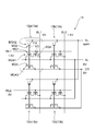
- FIG. 1 is a circuit diagram showing a circuit configuration of a nonvolatile semiconductor memory device of the present invention.
- FIG. 2 is a schematic diagram showing a layout of a circuit configuration of the memory cell shown in FIG. 1.
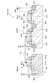
- FIG. 3 is a side sectional view showing a cross-sectional structure of the AA ′ portion and a cross-sectional structure of the BB ′ portion shown in FIG. 2. It is a circuit diagram which shows the voltage value of each site
- FIG. 1 is a circuit diagram showing a circuit configuration of a nonvolatile semiconductor memory device of the present invention.
- FIG. 2 is a schematic diagram showing a layout of a circuit configuration of the memory cell shown in FIG. 1.
- FIG. 3 is a side sectional view showing a cross-sectional structure
- FIG. 7 is a schematic diagram showing a layout of a circuit configuration of the memory cell shown in FIG. 6.
- FIG. 8 is a side cross-sectional view showing a cross-sectional structure of the AA ′ portion and a cross-sectional structure of the C-C ′ portion shown in FIG. 7. It is a circuit diagram which shows the circuit structure of the memory cell provided with the SRAM cell.
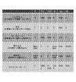
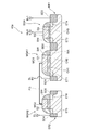
- FIG. 10 is a table showing voltage values of respective portions in the memory cell shown in FIG. 9 when data is programmed, erased, data loaded, written, read, and Vth monitor loaded. It is a sectional side view which shows the cross-section of the non-volatile semiconductor memory device by other embodiment.
- reference numeral 1 denotes a nonvolatile semiconductor memory device in which, for example, four memory cells 2a, 2b, 2c, 2d are arranged in 2 rows and 2 columns, and these memory cells 2a , 2b, 2c, 2d, for example, data can be written to the memory cell 2a arbitrarily selected by source side injection.
- the nonvolatile semiconductor memory device 1 is provided with two bit lines BL1 and BL2 and two word lines WL1 and WL2, and the bit lines BL1 and BL2 and the word lines WL1 and WL1 are provided.
- Memory cells 2a, 2b, 2c, 2d are arranged at positions where WL2 intersects.
- the erase line (erase line) EL is connected to the memory cells 2a, 2b, 2c, and 2d, and the memory cells 2a, 2b, 2c, and 2d are connected to the memory cells 2a, 2b, 2c, and 2d by the erase line EL.
- This voltage can be applied uniformly.
- the source line SL is connected to the memory cells 2a, 2b, 2c, 2d, and a predetermined voltage is uniformly applied to each memory cell 2a, 2b, 2c, 2d by the source line SL. It can be applied to.
- the memory cell 2a includes an N-type MOS memory MOS transistor (hereinafter referred to as a memory transistor) MGA1, a P-type MOS erase (erase) MOS transistor (hereinafter referred to as an erase transistor) MGA2, and an N-type MOS switch MOS.
- a transistor hereinafter referred to as a switch transistor
- SGA is provided, and the memory transistor MGA1 and the erase transistor MGA2 share one floating gate FG.
- the floating gate FG extends to each active region (described later) of the memory transistor MGA1 and the erase transistor MGA2, and can be a gate electrode MG1 of the memory transistor MGA1 and an erase gate electrode MG2 of the erase transistor MGA2.
- the memory cell 2a has a source line SL connected to the other memory cells 2b, 2c, and 2d connected to one end of the memory transistor MGA1, and also to the other memory cells 2b, 2c, and 2d.
- the connected erase line EL is connected to one end of the erase transistor MGA2.
- a bit line BL1 connected to another memory cell 2c arranged in one direction is connected to one end, and a word line WL1 connected to another memory cell 2b arranged in the other direction is connected to the switch gate electrode. It is connected to SG, and can be turned on / off by the voltage difference between the bit line BL1 and the word line WL1.
- the other end of the switch transistor SGA is electrically connected to the other end of the memory transistor MGA1, and is arranged in series with the memory transistor MGA1.
- the other end of the erase transistor MGA2 is short-circuited with a second active region described later.
- the area of the gate electrode MG1 of the memory transistor MGA1 is formed larger than the area of the erase gate electrode MG2 of the erase transistor MGA2, and the area of the gate electrode MG1 of the memory transistor MGA1 is increased.
- the potential from the memory transistor MGA1 is easily transmitted to the floating gate FG so that when writing data, a large current is generated in the memory transistor MGA1 so that a large amount of charge can be injected from the active region to the floating gate FG. Has been made.
- FIG. 2 is a schematic diagram showing an example of a layout for realizing the circuit configuration of the memory cell 2a shown in FIG.
- a P-type first active region ER1 is formed in the memory cell 2a, and the gate electrode MG1 of the memory transistor MGA1 and the switch gate electrode SG of the switch transistor SGA constituting the floating gate FG are the first.
- these memory transistor MGA1 and switch transistor SGA are arranged in series.
- an N-type second active region ER2 is formed in the memory cell 2a, and the erase gate electrode MG2 of the erase transistor MGA2 connected to the gate electrode MG1 of the memory transistor MGA1 is arranged in the second active region ER2.
- FIG. 3 is a cross-sectional view showing a side cross-sectional configuration of the AA ′ portion (right side in FIG. 3) and the B-B ′ portion (left side in FIG. 3) of FIG.
- the switch transistor SGA has a configuration in which source / drain regions SD2 and SD3 are formed at a distance in the first active region ER1, and the bit line BL1 is connected to the source / drain region SD3 which is one end thereof. Further, extension regions ET3 and ET4 are formed on the upper surface of the first active region ER1 between the source / drain regions SD2 and SD3 so as to be in contact with the side surfaces of the source / drain regions SD2 and SD3, and a channel region is formed between the extension regions ET3 and ET4.
- the switch transistor SGA has a switch gate electrode SG via a gate oxide film G3 on the channel region between the extension regions ET3 and ET4, and the word line WL1 is connected to the switch gate electrode SG.
- a sidewall SW that covers the side surface of the switch gate electrode SG is formed on the upper surfaces of the extension regions ET3 and ET4.
- the memory transistor MGA1 shares the source / drain region SD2 with the switch transistor SGA, and is arranged in series with the adjacent switch transistor SGA.
- the memory transistor MGA1 has a source / drain region SD1 formed in the first active region ER1 at a predetermined interval from the source / drain region SD2, and the source line SL is connected to the source / drain region SD1 at one end.
- a write voltage or the like can be applied to the source / drain region SD1 through the source line SL.
- the memory transistor MGA1 includes an extension region ET1 in contact with the side surface of the source / drain region SD1 at one end and an extension region (hereinafter referred to as a low concentration impurity extension region) in contact with the side surface of the source / drain region SD2 at the other end.
- ET2 is formed on the upper surface of the first active region ER1.
- the gate electrode MG1 that becomes the floating gate FG is formed on the upper surface of the first active region ER1 between the extension region ET1 and the low concentration impurity extension region ET2 via the gate oxide film G1, and the extension region Sidewalls SW that cover both side surfaces of the gate electrode MG1 are formed on the upper surfaces of the ET1 and the low-concentration impurity extension region ET2.
- the present invention is a low-concentration impurity formed in a sidewall lower region on the switch transistor SGA side (region between the lower region of the floating gate FG and the source / drain region SD2 on the other end side).
- the extension region ET2 is selected to have a lower impurity concentration than the extension region ET1 between the lower region of the floating gate FG and the source / drain region SD1 on one end side, and the low concentration impurity extension region ET2 is the extension region on the source line SL side. It is characterized in that it has a resistance value higher than that of ET1.
- the low concentration impurity extension region ET2 as a high resistance region preferably has an impurity doping amount of 1E18 / cm 3 or less.
- the memory transistor MGA1 having such a configuration has the largest potential drop in the low-concentration impurity extension region ET2 having a high resistance value when a large potential difference occurs between the source line SL and the bit line BL1 during data writing described later. It is made to occur.
- the upper surface of the first active region ER1 between the extension region ET1 and the low concentration impurity extension region ET2 has a depleted channel region CH1 in contact with the side surface of the extension region ET1, and this depletion
- an enhancement-type channel region CH2 whose both ends are in contact with the type channel region CH1 and the low-concentration impurity extension region ET2 is formed.
- the depleted channel region CH1 is in a depleted state by being doped with impurities such as arsenic and phosphorus.
- the channel region CH2 adjacent to the depleted channel region CH1 is in an enhanced state by being doped with impurities such as boron.
- the memory transistor MGA1 having such a configuration, when a write voltage is applied from the source line SL to the source / drain region SD1 at the time of data writing to be described later, the voltages of the depletion type channel region CH1 and the gate electrode MG1 rise synergistically. As a result, the voltage value finally applied to the end of the low-concentration impurity extension region ET2 can be increased to the voltage value applied to the source line SL (details will be described later).
- the erase transistor MGA2 has a configuration in which source / drain regions SD4 and SD5 are formed at intervals in a second active region ER2 formed separately from the first active region ER1, Of these, the erase line EL is connected to at least one source / drain region SD4.
- An extension region ET5 is formed on the upper surface of the second active region ER2 between the source / drain regions SD4 and SD5 so as to be in contact with the side surface of the source / drain region SD4, and the other side of the source / drain region SD5 is also in contact with the side surface.
- the extension region ET6 is formed.
- an erase gate electrode MG2 to be a floating gate FG is formed on the channel region between the extension regions ET5 and ET6 via the gate oxide film G2, and the erase gate electrode MG2 is connected to the memory transistor MGA1.
- the gate electrode MG1 is connected. Note that sidewalls SW are formed on the upper surfaces of the extension regions ET5 and ET6 so as to cover both side surfaces of the erase gate electrode MG2.
- FIG. 1 shows the voltage value of each part when data is written only to the memory cell 2a in the first row and first column among the plurality of memory cells 2a, 2b, 2c, and 2d.
- the memory cell 2a to which data is written is called a selected memory cell 3a
- the memory cells 2b, 2c, and 2d to which data is not written are called unselected memory cells 3b.
- a low voltage of 0 [V] is applied to the erase line EL and a high voltage of 6 [V] is applied to the source line SL during data writing. Can be applied.
- a voltage of 0 [V] is uniformly applied from the erase line EL to each erase transistor MGA2 of the memory cells 2a, 2b, 2c, 2d, and the memory cells 2a, 2b, 2c , 2d can be uniformly applied with a write voltage of 6 [V] from the source line SL.
- 1.5 [V] is applied to the switch transistor SGA of the selected memory cell 3a from the word line WL1 to the switch gate electrode SG, and a write voltage of 0 [V] is applied to one end from the bit line BL1 to turn it on. It can be a state.
- the switch transistor SGA when the switch transistor SGA is turned on, the source / drain region SD2 shared with the memory transistor MGA1 becomes 0 [V], which is the same as the bit line BL1.
- a write voltage of 6 [V] is applied from the source line SL to the source / drain region SD1 at one end, and the channel potential rises, and the channel region CH2 Can rise to the write voltage.
- the memory transistor MGA1 since the depletion type channel region CH1 is formed so as to be in contact with the side surface of the extension region ET1, the memory transistor MGA1 is in a depleted state in the depletion type channel region CH1 at the time of data writing.
- the channel voltage can be increased up to the threshold voltage Vth (Vth ⁇ 0).
- Vth the threshold voltage
- 6 [V] is applied to the source line SL during data writing.
- the depletion type channel region CH1 may rise to 2 [V].
- the potential of the gate electrode MG1 rises in proportion to the potential of the depletion type channel region CH1 due to capacitive coupling.
- the capacity ratio to the total capacity of the gate electrode MG1 (capacity ratio between the gate electrode MG1 and the depletion type channel region CH1) is 0.5
- the depletion type channel region CH1 of the gate electrode MG1 rises to a voltage of 2 [V].
- the potential increases from 0 [V] to 1 [V].
- the larger the capacitance ratio the higher the voltage rise efficiency of the gate electrode MG1. Therefore, it is desirable that the area of the gate electrode MG1 of the memory transistor MGA1 be larger than the erase gate electrode MG2 of the erase transistor MGA2. .
- the potential of the gate electrode MG1 rises to 1 [V]
- the allowable potential that can be applied to the depletion type channel region CH1 also rises, and the potential of the depletion type channel region CH1 further increases by 1 [V]. It rises to 3 [V].
- the potential of the gate electrode MG1 of the memory transistor MGA1 changes in proportion to the potential of the depletion type channel region CH1 due to capacitive coupling, and the depletion type channel region CH1 becomes the voltage 3 [V]. Increases from V] to 1.5 [V].
- the depleted channel region CH1 rises in synergy with the potential of the gate electrode MG1, and if the channel region CH2 is also turned on, the potential also contributes to capacitive coupling, and the potential of the gate electrode MG1 is It further rises and finally the potential of the channel region CH2 can reach a value close to 6 [V] applied to the source line SL.
- the end in contact with the channel region CH2 becomes 6 [V] which is the write voltage
- the end in contact with the source / drain region SD2 becomes 0 [V]
- 6 [V A high voltage difference is generated and a strong electric field is generated.
- the charge in the low-concentration impurity extension region ET2 is accelerated by the strong electric field generated in the low-concentration impurity extension region ET2, and a part of the secondary charge generated from the charge becomes a floating gate FG. It can be injected into the electrode MG1.
- charges can be accumulated in the floating gate FG, and data can be written.
- the selected memory cell 3a has a single-layer gate structure in which the gate electrode MG1 of the memory transistor MGA1, the erase gate electrode MG2 of the erase transistor MGA2, and the switch gate electrode SG of the switch transistor SGA are all provided as a single layer.
- the gate electrode MG1 of the memory transistor MGA1, the erase gate electrode MG2 of the erase transistor MGA2, and the switch gate electrode SG of the switch transistor SGA are all provided as a single layer.
- the low-concentration impurity extension region ET2 has a high resistance value with a low impurity concentration, and a large voltage drop occurs during data writing, but the adjacent source / drain region SD2 is suppressed to near 0 [V]. Therefore, it is possible to prevent a high write voltage from being applied to the switch transistor SGA.
- the gate oxide film G3 does not need to be as thick as the gate oxide film G1 (about 7 [nm]) of the memory transistor MGA1.
- nm] and a core MOS having a thin gate oxide film generally used in a nonvolatile memory can be used as it is.
- a write inhibit voltage of 1.5 [V] is applied to the bit line BL2 to which only the non-selected memory cell 3b is connected and A voltage of 0 [V] is applied to the word line WL2 to which only the selected memory cell 3b is connected.
- 1.5 [V] or 0 [V] is applied from the word lines WL1 and WL2 to the switch gate electrode SG of the switch transistor SGA.
- this nonvolatile semiconductor memory device by turning off the switch transistor SGA of the non-selected memory cell 3b, charge is not injected into the floating gate FG of the non-selected memory cell 3b, and the desired selected memory cell 3a It is possible to write data by injecting charges by source side injection only into the floating gate FG.
- the enhancement type channel region CH2 is also formed in the channel layer of the memory transistor MGA1 in addition to the depletion type channel region CH1 has been described.
- all the channel layers of the memory transistor MGA1 may be formed of the depleted channel region CH1.
- the depleted channel region CH1 is formed in the entire channel layer, it is necessary to increase the gate length of the gate electrode MG1 in consideration of the short channel effect.
- the channel concentration on the side close to the extension region ET1 and the channel concentration on the side close to the low concentration impurity extension region ET2 may be changed.
- the depletion type channel region CH1 and the enhancement type channel region CH2 are formed, it is preferable to select the depletion type channel region CH1 longer in the channel length direction than the channel region CH2, for example, the depletion type channel region CH1
- the channel region CH1: channel region CH2 is preferably X: 1 (X> 1). In this way, when the depletion type channel region CH1 is selected to be longer in the channel length direction than the channel region CH2, the floating potential at the time of the write operation is further increased. By increasing the electric field generated in the concentration impurity extension region ET2, the injection efficiency can be further increased.
- FIG. 1 shows the voltage values of the respective parts when reading the data of the memory cells 2a, 2b in the first row among the memory cells 2a, 2b, 2c, 2d. Is shown.
- the memory cells 2a and 2b that read data are referred to as read memory cells 6a
- the memory cells 2c and 2d that do not read data are referred to as non-read memory cells 6b.
- the nonvolatile semiconductor memory device 1 precharges the bit lines BL1 and BL2 connected to the read memory cell 6a by applying a read voltage of, for example, 1.5 [V] and is connected to the read memory cell 6a. Further, 1.5 [V] is applied to the word line WL1, the switch transistor SGA is turned on, and whether or not data is written can be determined based on the change in the read voltage of the bit lines BL1 and BL2.
- the memory transistor MGA1 is turned off and the read voltage on the bit line BL2 is 1.5 [V]. Will remain.
- the memory transistor MGA1 is turned on, whereby the read voltage of the bit line BL1 is reduced. It changes and becomes a voltage value lower than 1.5 [V] (for example, 0 [V]).
- the nonvolatile semiconductor memory device 1 detects the change in the read voltage of the bit lines BL1 and BL2, sets the 1.5 [V] bit line BL2 in which the read voltage does not change to “0”, and the other bit line in which the read voltage has changed.
- BL1 is set to “1”, and read information can be determined.
- the voltage values of the respective parts are shown in the case of using the hole injection caused by the band-to-band tunnel current.
- the erase transistor MGA2 A positive erase voltage 7 [V] is applied to the erase line EL, a low voltage 0 [V] is applied to the source line SL, and the bit lines BL1 and BL2 are opened.
- the erase voltage is applied collectively to the erase transistors MGA2 of the memory cells 2a, 2b, 2c, and 2d via the erase line EL, and, for example, charges are accumulated in the floating gate.
- the memory cell 2b holes can be injected from the channel layer of the erase transistor MGA2 into the floating gate FG, and data can be erased from the memory cells 2a, 2b, 2c, and 2d by mat batch processing.
- the gate electrode MG1 of the memory transistor MGA1 and the erase gate electrode MG2 of the erase transistor MGA2 are usually formed of polysilicon.
- the present invention is not limited to this, and for example, the memory transistor
- the gate electrode MG1 of MGA1 is doped with an impurity such as phosphorus to form an N-type gate electrode MG1, while the erase gate electrode MG2 of the erase transistor MGA2 that causes a band-to-band tunnel is doped with an impurity such as boron.
- the erase gate electrode MG2 may be used.
- the work function difference between the N-type gate electrode MG1 and the P-type erase gate electrode MG2 is 1 [V] or more, the N-type gate electrode MG1 and the P-type erase in the floating gate FG.
- a potential drop of about 1 [V] can be generated between the gate electrode MG2 and the generation of a band-to-band tunnel current in the erase transistor MGA2 compared to the case where a floating gate is formed only by an N-type gate electrode. Efficiency is improved and it becomes easier to inject holes into the floating gate FG.
- the memory cell 2a includes the single layer gate structure memory transistor MGA1 having the floating gate FG and the single layer gate structure switch transistor SGA having the switch gate electrode SG.
- the source line SL is connected to one end of the memory transistor MGA1
- the bit line BL1 is connected to one end of the switch transistor SGA
- the source / drain region SD2 is connected to the other end of the memory transistor MGA1 and the other end of the switch transistor.
- the memory transistor MGA1 and the switch transistor SGA are arranged in series.
- the extension region ET1 is formed on the side surface of the source / drain region SD1 at one end, and the low concentration impurity extension region ET2 is formed on the side surface of the source / drain region SD2 on the other end side electrically connected to the switch transistor SGA. Then, the impurity concentration of the low-concentration impurity extension region ET2 is made lower than that of the extension region ET1, and the resistance value of the low-concentration impurity extension region ET2 is increased.
- a write voltage of 6 [V] is applied from the source line SL to one end of the memory transistor MGA1, and 0 [V] is applied from the bit line BL1 to one end of the switch transistor SGA.
- the memory transistor MGA1 By being applied and turned on, the memory transistor MGA1 generates a strong electric field by causing a voltage drop of 6 [V] in the low-concentration impurity extension region ET2 on the side adjacent to the switch transistor SGA.
- Data can be written by so-called source side injection in which electric charges are injected into the floating gate FG by an electric field.
- the memory transistor MGA1 has a depleted channel region CH1 formed between the extension region ET1 and the low concentration impurity extension region ET2, and at the time of data writing, a write voltage of 6 [V] is applied to one end. Is applied, the voltage of the gate electrode MG1 serving as the floating gate FG and the voltage of the depleted channel region CH1 increase synergistically, and finally with respect to the low concentration impurity extension region ET2 on the other end side. The same 6 [V] as the write voltage applied to the source line SL can be applied, and a high voltage drop necessary for source-side injection can be generated in the low-concentration impurity extension region ET2.
- the switch transistor SGA adjacent to the memory transistor MGA1 can be suppressed to a low voltage, thus the gate oxide film G3 of the switch transistor SGA.
- the voltages applied to the bit lines BL1, BL2 and the word lines WL1, WL2 can be suppressed to 1.5 [V] or less, so that these bit lines BL1 , BL2 and the matrix selection circuit (not shown) for controlling the word lines WL1, WL2 can be designed with a core MOS (1.5V-MOS) on the premise of a low voltage, and the gate oxide film of the switch transistor SGA As G3 can be made thinner, high-speed operation can be achieved and the circuit area can be reduced.
- 1.5V-MOS 1.5V-MOS
- the memory transistor MGA1 and the switch transistor SGA all have a single-layer gate structure, but at the time of data writing, a high voltage is applied from the source line SL to one end of the memory transistor MGA1, and A low voltage is applied from the bit line BL1 to one end of the switch transistor SGA to turn it on, causing a voltage drop in the low concentration impurity extension region ET2 of the memory transistor MGA1 between the source line SL and the bit line BL1. A strong electric field is generated, and charges can be injected into the floating gate FG by source side injection using the strong electric field.
- the depletion type channel region CH1 is formed in the channel layer of the memory transistor MGA1, and the channel layer is generated by the synergistic effect of the floating gate FG and the depletion type channel region CH1.
- the present invention is not limited to this, and a cup in which the floating gate FG extends is shown in FIG.
- a ring capacitor MGA3 may be provided, and the potential of the floating gate FG may be raised by raising the coupling capacitor MGA3, thereby turning on the channel layer of the memory transistor MGA1.
- the channel layer of the memory transistor MGA1 is not formed with the depletion type channel region CH1 as shown in FIG. 3, but only the enhancement type channel region CH4 (described later in FIG. 8) is used for coupling.
- the channel region CH4 of the memory transistor MGA1 can be turned on by the high potential from the capacitor MGA3.
- FIG. 6 in which parts corresponding to those in FIG. 2 are assigned the same reference numerals is a schematic diagram showing an example of a layout for realizing the circuit configuration of the memory cell 12a shown in FIG.
- the N-type third active region ER3 is formed in the memory cell 12a
- the coupling gate electrode MG3 of the coupling capacitor MGA3 is formed in the third active region ER3
- the coupling gate Electrode MG3 is connected to erase gate electrode MG2 of erase transistor MGA2, and floating gate FG is formed by gate electrode MG1, erase gate electrode MG2, and coupling gate electrode MG3.
- FIG. 8 in which the same reference numerals are assigned to the corresponding parts in FIG. It is. However, FIG. 8 does not show each part according to the area of each part in FIG. 7 (for example, the coupling gate electrode MG3 is larger than the gate electrode MG1, but is shown smaller in FIG. 8). However, it only schematically shows a side sectional configuration of each part.
- a depletion type channel region CH1 (FIG. 3) is formed between the extension region ET1 and the low concentration impurity extension region ET2 in the memory transistor MGA1.
- the channel layer is entirely formed of only the enhancement type channel region CH4.
- P-type source / drain regions SD7 and SD8 are formed at an interval in the N-type third active region ER3, and a coupling gate line CG is connected to the source / drain region SD7 at one end. ing.
- the coupling gate line CG is also connected to the source / drain region SD6 of another adjacent coupling capacitor (not shown) formed via the element isolation layer 15.
- SD6 is N-type and is a power supply region to the well.
- the coupling capacitor MGA3 includes an extension region ET8 in contact with the side surface of the source / drain region SD7 at one end and a side surface of the source / drain region SD8 at the other end on the upper surface of the third active region ER3 between the source / drain regions SD7 and SD8.
- An extension region ET9 in contact therewith is formed.
- a coupling gate electrode MG3 to be a floating gate FG is formed on the channel layer between the P-type extension regions ET8 and ET9 via the gate oxide film G4.
- a sidewall SW is formed on the upper surface so as to cover both side surfaces of the coupling gate electrode MG3.
- FIG. 6 shows the voltage value of each part when writing data only to the memory cell 12a in the first row and the first column among the plurality of memory cells 12a, 12b, 12c, and 12d.
- this nonvolatile semiconductor memory device 11 uniformly applies a write voltage of 8 [V] to the coupling capacitor MGA3 of each of the memory cells 12a, 12b, 12c, and 12d by the coupling gate line CG when writing data. Open the erase line EL.
- the selected memory cell 13a into which data is written is generated between the coupling capacitor MGA3 and the floating gate FG when a write voltage of 8 [V] is applied to the coupling gate line CG. Due to the capacitive coupling, the potential of the floating gate FG rises by the capacitance ratio, whereby the memory transistor MGA1 to which the source line SL is connected is turned on, and the potential of the source line SL is transmitted to the channel region CH4 of the memory transistor MGA1.
- the strength required for source-side implantation in the low-concentration impurity extension region ET2 is increased. An electric field is generated, and by this strong electric field, charges can be injected into the floating gate FG, and data can be written.
- the coupling gate electrode MG3 of the coupling capacitor MGA3 has a larger area than the gate electrode MG1 of the memory transistor MGA1 and the erase gate electrode MG2 of the erase transistor MGA2, thereby increasing the capacitance ratio. be able to.
- the potential at the end of the channel region CH4 in contact with the low concentration impurity extension region ET2 in the memory transistor MGA1 is increased to the same level as the potential of the source line SL. It becomes possible.
- FIG. 9 shows a nonvolatile semiconductor memory device 31 according to the present invention, in which an SRAM cell 32 is connected to a nonvolatile memory section 33 comprising memory cells 2a and 2b. Characterized by points.
- the non-volatile memory section 33 forms a 2-cell / 1-bit complementary cell by the memory cell 2a and the memory cell 2b.
- the SRAM cell 32 includes access transistors 35a and 35b made of N-type MOS transistors, load transistors 36a and 36b made of P-type MOS transistors, and drive transistors 37a and 37b made of N-type MOS transistors. It is composed of a number of MOS transistors.
- the load transistor 36a (36b) has a drain connected to the drain of the drive transistor 37a (37b), a source connected to the power supply line Vpp, and a gate connected to the gate of the drive transistor 37a (37b).
- the source of the drive transistor 37a (37b) is connected to the ground line GND.
- the access transistor 35a has a drain connected to the complementary first bit line BLT, and a source connected to the storage node Ca between the load transistor 36a and the drive transistor 37a and the gates of the load transistor 36b and the drive transistor 37b.
- the drain of the other access transistor 35b is also connected to the complementary second bit line BLB, and the source is connected to the storage node Cb between the load transistor 36b and the drive transistor 37b and to the gates of the load transistor 36a and the drive transistor 37a. Is connected.
- these access transistors 35a and 35b have gates connected to a common word line WL, and a latch-type sense amplifier (not shown) is connected between the complementary first bit line BLT and the complementary second bit line BLB. Yes.
- the SRAM cell 32 is connected to the bit line BL1 of one memory cell 2a to one storage node Ca, and to the bit line BL2 of the other memory cell 2b to the other storage node Cb.
- the non-volatile memory section 33 has substantially the same configuration as the memory cells 2a and 2b shown in FIG. 1 described in the above embodiment, but here, each switch transistor SGA and SGA b has its own switch gate. line RG1, and provided RG2, are constituted each switch transistor SGA, SGA b the like each may separately on-off control.
- the nonvolatile memory unit 33 since the SRAM cell 32 and the nonvolatile memory unit 33 can be blocked by the switch transistors SGA and SGA b , the nonvolatile memory unit 33 is switched to the switch transistor at the time of external write operation or read operation. They can be separated by SGA and SGA b and used as a general SRAM cell 32. Further, the SRAM cell 32 can be operated only by Vdd, and can be constructed using a normal core MOS, so that high speed operation is possible.
- the nonvolatile semiconductor memory device 31 having such a configuration is configured to perform external data writing and reading with the SRAM cell 32.
- the data to be written to the memory cells 2a and 2b is stored in the SRAM cell 32 directly connected to the memory cells 2a and 2b.
- the source side injection performed in the nonvolatile memory section 33 consumes less power, the write potential control can be performed in a mat.
- the power consumption in the nonvolatile semiconductor memory device 31 by changing the voltage applied to the switch gate lines RG1 and RG2, only one of the switch transistors SGA and SGA b is turned on. , Power consumption can be reduced.
- the switch transistor SGA which is turned to reduce the number of SGA b, it is also possible to reduce power consumption during writing.
- FIG. 10 shows the nonvolatile semiconductor memory device 31 at the time of programming to capture data from the SRAM cell 32 to the nonvolatile memory unit 33 (denoted as “program” in FIG. 10) and at the time of erasing data in the nonvolatile memory unit 33.
- program in FIG. 10
- data load when data is loaded again from the nonvolatile memory 33 to the SRAM cell 32
- data write when data is written to the SRAM cell 32
- read when reading data from the SRAM cell 32
- Vth Vth
- the voltage value of each part of “Monitor load” is shown. In FIG. 10, a portion that can be set to an arbitrary voltage value is described as “Don't care”.
- the memory cell 2a and the memory cell 2b are composed of 2 cells / 1-bit complementary cells, if both switch transistors SGA and SGA b are turned on, they are complemented depending on the state of the complementary cell. Because the potential of the bit line on the side changes, for example, a latch circuit (not shown) sets the bit line BL1 on the side where the voltage has dropped earlier to ⁇ 1 '', and forcibly moves the other bit line BL2 side accordingly will be set to "0", there is a problem in that it does not allow to be normal monitoring of the memory transistor MGA1, MGA1 b of the Vth.
- switch gate lines RG1 and RG2 are provided for the switch transistors SGA and SGA b , respectively, and the switch transistors SGA and SGA are provided.
- b was turned on and off individually, and the Vth of each memory transistor MGA1, MGA1 b of the memory cell 2a and the memory cell 2b is made to be able to monitor individually.
- data write to the SRAM cell 32 is performed by applying a predetermined voltage of Vdd to the word line WL and connecting both the access transistors 35a and 35b connected to the word line WL. Turn on. At this time, a predetermined voltage of Vdd can also be applied to the power supply line Vpp. In the SRAM cell 32, for example, when Vdd is applied as a write voltage to one complementary first bit line BLT, 0 [V] may be applied as a write inhibit voltage to the other complementary second bit line BLB.
- the complementary second bit line BLB and the gate are electrically connected via the other access transistor 35b, so that 0 [V] is applied to the gate.
- the load transistor 36a is turned on and the drive transistor 37a is turned off.
- the storage node Ca between the load transistor 36a and the drive transistor 37a is electrically connected to the power supply line Vpp via the load transistor 36a, and the voltage becomes High (“1”).
- Vdd is applied to the gate by electrically connecting the complementary first bit line BLT and the gate through one access transistor 35a.
- the transistor 36b is turned off and the drive transistor 37b is turned on.
- the storage node Cb between the load transistor 36b and the drive transistor 37b is electrically connected to the ground line GND via the drive transistor 37b, and the voltage becomes Low (“0”).
- the SRAM cell 32 data is written.
- the nonvolatile memory unit 33 In this case, in the nonvolatile memory unit 33, 0 [V] is applied to the erase line EL, 6 [V] is applied to the source line SL, and Vdd is applied to the switch gate lines RG1 and RG2, respectively. SGA and SGA b are on.
- the switch transistor SGA of the memory cell 2a since the switch transistor SGA of the memory cell 2a is electrically connected to one storage node Ca to which data is written via one bit line BL1, one end of the switch transistor SGA is connected to one storage node Ca. It becomes the same high potential as the storage node Ca.
- the memory transistor MGA1 since the potential difference between the switch transistor SGA side and the source line SL side becomes small, a strong electric field is not generated, and charge cannot be injected into the floating gate FG.
- the nonvolatile memory 33 to the other storage node Cb in which data is not written, via the other bit line BL2 because the switch transistor SGA b of the other memory cell 2b are electrically connected one end of the switch transistor SGA b becomes the potential of the same Low storage node Cb.
- the memory transistor MGA1 b charge on the floating gate FG strong electric field is generated from the potential difference between the switch transistor SGA b side and the source line SL side increases can be injected.
- the data once taken into the nonvolatile memory section 33 as described above can be rewritten to the SRAM cell 32 by the mat batch processing based on the principle of “(3) data read operation” described above. it can.
- the nonvolatile memory unit 33 the charge is accumulated in the floating gate FG of the memory cell 2b and the data is written, and the charge is not accumulated in the floating gate FG of the memory cell 2a and the data is not written. State. At this time, it is assumed that no data is written in the storage nodes Ca and Cb.
- 0 [V] is applied to the word line WL, and the access transistors 35a and 35b are turned off.
- 0 [V] is applied to the erase line EL
- 3 [V] is applied to the source line SL
- Vdd is applied to the switch gate lines RG1 and RG2, respectively.
- SGA b is on.
- the non-volatile memory unit 33 is electrically connected between the memory transistor MGA1 and the bit line BL1, and one storage node Ca of the SRAM cell 32 is generated in accordance with the high potential of the floating gate FG (a state in which electrons are not accumulated). Can be restored to a state in which data is written ("1").
- the nonvolatile memory section 33 is also electrically connected between the memory transistor MGA b and the bit line BL2, and the other storage node of the SRAM cell 32 in accordance with the low potential of the floating gate FG (a state where electrons are accumulated). The state can be restored to a state where data is not written (“0”) by lowering Cb. Further, in the nonvolatile memory section 33, the data load to the SRAM cell 32 can be performed by mat batch processing, so that control of peripheral circuits can be simplified.
- data can be erased in the nonvolatile memory unit 33 based on the principle of “(4) Data erasing operation” described above.
- an erase voltage of 7 [V] can be applied to the erase line EL, and 0 [V] can be applied to the source line SL and the switch gate lines RG1 and RG2.
- Nonvolatile memory portion 33 the erase transistors MGA2 connected to erase lines EL, that MGA2 b strong electric field only to the gate electrode of the is applied, the charge in the floating gates FG by the erase transistor MGA2, MGA2 b channel layer And the data in the nonvolatile memory section 33 can be erased by batch mat processing.
- the program to the nonvolatile memory unit 33 is as follows. Done. In the nonvolatile memory section 33 provided with only one memory cell 2a, 0 [V] is applied to the erase line EL, 6 [V] is applied to the source line SL, and Vdd is further applied to the switch gate line RG1. The switch transistor SGA is in the on state.
- the switch transistor SGA of the memory cell 2a is electrically connected to one storage node Ca to which data is written via one bit line BL1, one end of the switch transistor SGA is connected to one storage node Ca. It becomes the same high potential as the storage node Ca.
- the potential difference between the switch transistor SGA side and the source line SL side becomes small, so that a strong electric field is not generated and charge cannot be injected into the floating gate FG. In this manner, in the nonvolatile memory unit 33, the data recorded in the SRAM cell 32 is taken into only one memory cell 2a.
- 0 [V] is applied to the word line WL, and the access transistors 35a and 35b are turned off.
- 0 [V] is applied to the erase line EL
- 3 [V] is applied to the source line SL
- Vdd is applied to the switch gate line RG1, so that the switch transistor SGA is turned on. It has become.
- the memory cell 2a is electrically connected between the memory transistor MGA1 and the bit line BL1, and the one storage node Ca of the SRAM cell 32 is connected with the high potential of the floating gate FG (a state in which no electrons are accumulated). It can be restored to a state where data is written (“1”) at a high potential.
- the load transistor 36a connected to the storage node Ca is turned off, while the drive transistor 37b is turned on to perform storage.
- the node Ca is connected to the ground line GND and becomes a low potential, and the storage node Cb can be restored to a state where data is not written (“0”).
- the data write state is determined for one storage node Ca of the SRAM cell 32, the data write state is also determined for the other storage node Cb.
- Data loading to the SRAM cell 32 can be performed with only one memory cell 2a provided in the memory section 33.
- the circuit configuration can be further simplified because the other memory cell 2b is not provided.
- a depletion type channel region CH1 and an enhancement type channel region CH2 as shown in FIG. 3 are formed in the channel layer of the memory transistor MGA1. It may be.
- nonvolatile semiconductor memory device 31 shown in FIG. 9 the case where the nonvolatile memory portion 33 to which the memory cells 2a and 2b shown in FIG. 1 are applied is described, but the present invention is not limited to this.
- a nonvolatile memory unit to which the memory cells 12a and 12b provided with the coupling capacitor MGA3 shown in FIG. 6 are applied may be provided.
- the voltage values at the time of data writing, at the time of erasing data, at the time of reading data are specified, but the present invention is not limited to this.
- Various voltage values may be applied.
- a voltage of 1.5 [V] is applied to the bit lines BL1 and BL2 and the word lines WL1 and WL2 to control the on / off of the switch transistor SGA has been described.
- the present invention is not limited to this, and it is sufficient that the switch transistor SGA can be controlled on and off. Therefore, even if 1.2 [V] is applied to the bit lines BL1 and BL2 and the word lines WL1 and WL2, A core MOS (1.2V-MOS) can be used as the switch transistor SGA.
- the erase transistor MGA2 is formed in the P-type second active region and the memory transistor MGA1 and the switch transistor SGA are formed in the P-type first active region has been described.
- the invention is not limited to this, and the erase transistor MGA2 may be formed in the N-type second active region, and the memory transistor MGA1 and the switch transistor SGA may be formed in the N-type first active region, as shown in FIG.
- the coupling capacitor MGA3 may be formed in the P-type third active region.
- the memory cell 2a includes the erase transistor MGA2 and the data in the memory cell 2a can be erased has been described.
- the present invention is not limited to this, for example, the memory
- the memory cell may be configured by only the switch transistor SGA and the memory transistor MGA1.
- a nonvolatile semiconductor memory device including such a memory cell can be a nonvolatile element that can be written only once to the memory transistor MGA1.
- the enhancement type channel region CH2 is formed as it is to the source / drain region SD2, and the floating gate FG A part of the channel region CH2 between the lower region and the source / drain region SD2 on the other end side may be used as the high resistance region WA.
- a write voltage of 6 [V] is applied from the source line SL to one end of the memory transistor MGA1 during data writing, and the bit line BL1 as in the above-described embodiment.
- 0 [V] is applied to one end of the switch transistor SGA to turn on, and in the memory transistor MGA1, a voltage drop of 6 [V] occurs in the high resistance region WA on the side adjacent to the switch transistor SGA.
- a strong electric field is generated, and data can be written by so-called source side injection in which charges are injected into the floating gate FG by this strong electric field.
- the impurity concentration of the channel region CH2 is 1E18 / cm 3 or less.
- the configuration in which the channel region is formed up to the source / drain region SD2 without providing the low-concentration impurity extension region ET2 and the channel region in the lower region of the sidewall SW is the high resistance region WA is shown in FIG.
- the present invention can also be applied to the memory transistor MGA1 shown.
- the channel region CH4 can be directly extended to the source / drain region SD2.
- the extension on one end side is the same as the other end side.
- the depleted channel region CH1 may be formed as it is up to the source / drain region SD1 without providing the region ET1.
- the channel region CH2 is a depletion type channel region instead of an enhancement type, and this depletion type channel region is formed as it is up to the source / drain region SD2, and the lower region of the floating gate FG and the source / drain region SD2 on the other end side are formed. A part of the depletion type channel region between them may be a high resistance region WA.
- the resistance value of the high resistance region WA can be formed to be higher than the resistance value of the extension region ET1. Even if the depletion type channel region CH1 is formed from the lower region of the floating gate FG to the source / drain region SD1 without providing the extension region ET1 on one end side, the depletion between the lower region of the floating gate FG and the source / drain region SD2 is performed. The resistance value of the type channel region can be formed to be higher than the resistance value of the depletion type channel region CH1 on one end side.
Landscapes
- Engineering & Computer Science (AREA)
- Microelectronics & Electronic Packaging (AREA)
- Non-Volatile Memory (AREA)
- Read Only Memory (AREA)
- Semiconductor Memories (AREA)
- Static Random-Access Memory (AREA)
Priority Applications (2)
| Application Number | Priority Date | Filing Date | Title |
|---|---|---|---|
| US14/647,009 US9646979B2 (en) | 2012-11-27 | 2013-10-31 | Non-volatile semiconductor storage device |
| TW102139904A TWI582909B (zh) | 2012-11-27 | 2013-11-04 | Nonvolatile semiconductor memory device |
Applications Claiming Priority (2)
| Application Number | Priority Date | Filing Date | Title |
|---|---|---|---|
| JP2012-259128 | 2012-11-27 | ||
| JP2012259128A JP6053474B2 (ja) | 2012-11-27 | 2012-11-27 | 不揮発性半導体記憶装置 |
Publications (1)
| Publication Number | Publication Date |
|---|---|
| WO2014083997A1 true WO2014083997A1 (ja) | 2014-06-05 |
Family
ID=50827643
Family Applications (1)
| Application Number | Title | Priority Date | Filing Date |
|---|---|---|---|
| PCT/JP2013/079512 Ceased WO2014083997A1 (ja) | 2012-11-27 | 2013-10-31 | 不揮発性半導体記憶装置 |
Country Status (4)
| Country | Link |
|---|---|
| US (1) | US9646979B2 (enExample) |
| JP (1) | JP6053474B2 (enExample) |
| TW (1) | TWI582909B (enExample) |
| WO (1) | WO2014083997A1 (enExample) |
Cited By (1)
| Publication number | Priority date | Publication date | Assignee | Title |
|---|---|---|---|---|
| CN110190060A (zh) * | 2018-02-23 | 2019-08-30 | 爱思开海力士系统集成电路有限公司 | 编程效率增强的一次性可编程存储器件及其制造方法 |
Families Citing this family (8)
| Publication number | Priority date | Publication date | Assignee | Title |
|---|---|---|---|---|
| JP6306466B2 (ja) | 2014-07-31 | 2018-04-04 | 株式会社フローディア | 不揮発性sramメモリセル、および不揮発性半導体記憶装置 |
| US9450052B1 (en) * | 2015-07-01 | 2016-09-20 | Chengdu Monolithic Power Systems Co., Ltd. | EEPROM memory cell with a coupler region and method of making the same |
| US10892266B2 (en) * | 2016-01-19 | 2021-01-12 | Ememory Technology Inc. | Nonvolatile memory structure and array |
| US9847133B2 (en) * | 2016-01-19 | 2017-12-19 | Ememory Technology Inc. | Memory array capable of performing byte erase operation |
| US11361215B2 (en) * | 2017-11-29 | 2022-06-14 | Anaflash Inc. | Neural network circuits having non-volatile synapse arrays |
| WO2019124356A1 (ja) | 2017-12-20 | 2019-06-27 | パナソニック・タワージャズセミコンダクター株式会社 | 半導体装置及びその動作方法 |
| US11462282B2 (en) | 2020-04-01 | 2022-10-04 | Taiwan Semiconductor Manufacturing Co., Ltd. | Semiconductor memory structure |
| CN114005477B (zh) * | 2021-11-03 | 2023-03-10 | 中国电子科技集团公司第五十八研究所 | 一种高可靠共浮栅型Flash存内计算器件及阵列结构 |
Citations (5)
| Publication number | Priority date | Publication date | Assignee | Title |
|---|---|---|---|---|
| EP0298657A2 (en) * | 1987-07-09 | 1989-01-11 | Fujitsu Limited | Non-volatile random access memory device having volatile memory cell |
| US20040012039A1 (en) * | 2002-05-10 | 2004-01-22 | Riichiro Shirota | Non-volatile semiconductor memory device |
| US20090080257A1 (en) * | 2007-09-25 | 2009-03-26 | Renesas Technology Corp. | Semiconductor device |
| JP2009194140A (ja) * | 2008-02-14 | 2009-08-27 | Renesas Technology Corp | 半導体装置およびその製造方法 |
| JP2009267185A (ja) * | 2008-04-28 | 2009-11-12 | Sharp Corp | 不揮発性半導体記憶装置 |
Family Cites Families (11)
| Publication number | Priority date | Publication date | Assignee | Title |
|---|---|---|---|---|
| JPH0760864B2 (ja) | 1984-07-13 | 1995-06-28 | 株式会社日立製作所 | 半導体集積回路装置 |
| US5181188A (en) * | 1989-07-07 | 1993-01-19 | Sharp Kabushiki Kaisha | Semiconductor memory device |
| US5331188A (en) * | 1992-02-25 | 1994-07-19 | International Business Machines Corporation | Non-volatile DRAM cell |
| US5592415A (en) * | 1992-07-06 | 1997-01-07 | Hitachi, Ltd. | Non-volatile semiconductor memory |
| JPH11186416A (ja) * | 1997-12-19 | 1999-07-09 | Rohm Co Ltd | 不揮発性半導体記憶装置およびその製造方法 |
| US6114724A (en) * | 1998-03-31 | 2000-09-05 | Cypress Semiconductor Corporation | Nonvolatile semiconductor memory cell with select gate |
| US7209392B2 (en) * | 2004-07-20 | 2007-04-24 | Ememory Technology Inc. | Single poly non-volatile memory |
| KR100795907B1 (ko) * | 2006-09-07 | 2008-01-21 | 삼성전자주식회사 | 이이피롬 소자 및 그 형성 방법 |
| JP5316532B2 (ja) * | 2008-03-31 | 2013-10-16 | 富士通セミコンダクター株式会社 | 半導体装置 |
| US8674422B2 (en) * | 2012-01-30 | 2014-03-18 | Synopsys, Inc. | Asymmetric dense floating gate nonvolatile memory with decoupled capacitor |
| US9001580B1 (en) * | 2013-12-04 | 2015-04-07 | Synopsys, Inc. | Asymmetric dense floating gate nonvolatile memory with decoupled capacitor |
-
2012
- 2012-11-27 JP JP2012259128A patent/JP6053474B2/ja active Active
-
2013
- 2013-10-31 WO PCT/JP2013/079512 patent/WO2014083997A1/ja not_active Ceased
- 2013-10-31 US US14/647,009 patent/US9646979B2/en active Active
- 2013-11-04 TW TW102139904A patent/TWI582909B/zh active
Patent Citations (14)
| Publication number | Priority date | Publication date | Assignee | Title |
|---|---|---|---|---|
| EP0298657A2 (en) * | 1987-07-09 | 1989-01-11 | Fujitsu Limited | Non-volatile random access memory device having volatile memory cell |
| JPS6414798A (en) * | 1987-07-09 | 1989-01-18 | Fujitsu Ltd | Non-volatile memory device |
| US5029132A (en) * | 1987-07-09 | 1991-07-02 | Fujitsu Limited | Random access memory device having parallel non-volatile memory cells |
| KR910007402B1 (en) * | 1987-07-09 | 1991-09-25 | Fujitsu Corp | Nonvolatile ram with volatile memorycell |
| DE3852222T2 (de) * | 1987-07-09 | 1995-04-06 | Fujitsu Ltd | Nichtflüchtige RAM-Vorrichtung mit flüchtigen Speicherzellen. |
| JP2004031920A (ja) * | 2002-05-10 | 2004-01-29 | Toshiba Corp | 不揮発性半導体記憶装置 |
| US20040012039A1 (en) * | 2002-05-10 | 2004-01-22 | Riichiro Shirota | Non-volatile semiconductor memory device |
| US20090080257A1 (en) * | 2007-09-25 | 2009-03-26 | Renesas Technology Corp. | Semiconductor device |
| KR20090031841A (ko) * | 2007-09-25 | 2009-03-30 | 가부시끼가이샤 르네사스 테크놀로지 | 반도체 장치 |
| JP2009081181A (ja) * | 2007-09-25 | 2009-04-16 | Renesas Technology Corp | 半導体装置 |
| TW200924171A (en) * | 2007-09-25 | 2009-06-01 | Renesas Tech Corp | Semiconductor device |
| US20110024814A1 (en) * | 2007-09-25 | 2011-02-03 | Renesas Electronics Corporation | Semiconductor Device |
| JP2009194140A (ja) * | 2008-02-14 | 2009-08-27 | Renesas Technology Corp | 半導体装置およびその製造方法 |
| JP2009267185A (ja) * | 2008-04-28 | 2009-11-12 | Sharp Corp | 不揮発性半導体記憶装置 |
Cited By (2)
| Publication number | Priority date | Publication date | Assignee | Title |
|---|---|---|---|---|
| CN110190060A (zh) * | 2018-02-23 | 2019-08-30 | 爱思开海力士系统集成电路有限公司 | 编程效率增强的一次性可编程存储器件及其制造方法 |
| CN110190060B (zh) * | 2018-02-23 | 2024-01-09 | 爱思开海力士系统集成电路有限公司 | 编程效率增强的一次性可编程存储器件及其制造方法 |
Also Published As
| Publication number | Publication date |
|---|---|
| JP6053474B2 (ja) | 2016-12-27 |
| TW201448122A (zh) | 2014-12-16 |
| US9646979B2 (en) | 2017-05-09 |
| JP2014107406A (ja) | 2014-06-09 |
| TWI582909B (zh) | 2017-05-11 |
| US20150311219A1 (en) | 2015-10-29 |
Similar Documents
| Publication | Publication Date | Title |
|---|---|---|
| JP6053474B2 (ja) | 不揮発性半導体記憶装置 | |
| US7382658B2 (en) | Non-volatile memory embedded in a conventional logic process and methods for operating same | |
| US9362374B2 (en) | Simple and cost-free MTP structure | |
| KR101670619B1 (ko) | 불휘발성 반도체 기억 장치 | |
| US8552763B2 (en) | Switch array including active regions being adjacent to each other in channel width direction of memory cell transistor | |
| JP2014183233A (ja) | 不揮発性半導体記憶装置 | |
| US7675779B2 (en) | Non-volatile memory devices and methods of operating the same | |
| US8144514B2 (en) | One-transistor floating-body DRAM cell device with non-volatile function | |
| KR102512901B1 (ko) | 불휘발성 sram 메모리 셀, 및 불휘발성 반도체 기억 장치 | |
| JP6383280B2 (ja) | 不揮発性半導体記憶装置 | |
| JP6069137B2 (ja) | 不揮発性半導体記憶装置 | |
| JP6175171B2 (ja) | 不揮発性sramメモリセル、および不揮発性半導体記憶装置 | |
| US9424924B2 (en) | Non-volatile semiconductor memory device having depletion-type and enhancement-type channel regions |
Legal Events
| Date | Code | Title | Description |
|---|---|---|---|
| 121 | Ep: the epo has been informed by wipo that ep was designated in this application |
Ref document number: 13859380 Country of ref document: EP Kind code of ref document: A1 |
|
| WWE | Wipo information: entry into national phase |
Ref document number: 14647009 Country of ref document: US |
|
| NENP | Non-entry into the national phase |
Ref country code: DE |
|
| 122 | Ep: pct application non-entry in european phase |
Ref document number: 13859380 Country of ref document: EP Kind code of ref document: A1 |