WO2014065311A1 - 荷電粒子線装置及び重ね合わせずれ量測定方法 - Google Patents
荷電粒子線装置及び重ね合わせずれ量測定方法 Download PDFInfo
- Publication number
- WO2014065311A1 WO2014065311A1 PCT/JP2013/078678 JP2013078678W WO2014065311A1 WO 2014065311 A1 WO2014065311 A1 WO 2014065311A1 JP 2013078678 W JP2013078678 W JP 2013078678W WO 2014065311 A1 WO2014065311 A1 WO 2014065311A1
- Authority
- WO
- WIPO (PCT)
- Prior art keywords
- charged particle
- particle beam
- pattern
- amount
- overlay deviation
- Prior art date
- Legal status (The legal status is an assumption and is not a legal conclusion. Google has not performed a legal analysis and makes no representation as to the accuracy of the status listed.)
- Ceased
Links
Images

Classifications
-
- H—ELECTRICITY
- H01—ELECTRIC ELEMENTS
- H01J—ELECTRIC DISCHARGE TUBES OR DISCHARGE LAMPS
- H01J37/00—Discharge tubes with provision for introducing objects or material to be exposed to the discharge, e.g. for the purpose of examination or processing thereof
- H01J37/02—Details
- H01J37/22—Optical, image processing or photographic arrangements associated with the tube
- H01J37/222—Image processing arrangements associated with the tube
-
- G—PHYSICS
- G01—MEASURING; TESTING
- G01B—MEASURING LENGTH, THICKNESS OR SIMILAR LINEAR DIMENSIONS; MEASURING ANGLES; MEASURING AREAS; MEASURING IRREGULARITIES OF SURFACES OR CONTOURS
- G01B15/00—Measuring arrangements characterised by the use of electromagnetic waves or particle radiation, e.g. by the use of microwaves, X-rays, gamma rays or electrons
-
- G—PHYSICS
- G03—PHOTOGRAPHY; CINEMATOGRAPHY; ANALOGOUS TECHNIQUES USING WAVES OTHER THAN OPTICAL WAVES; ELECTROGRAPHY; HOLOGRAPHY
- G03F—PHOTOMECHANICAL PRODUCTION OF TEXTURED OR PATTERNED SURFACES, e.g. FOR PRINTING, FOR PROCESSING OF SEMICONDUCTOR DEVICES; MATERIALS THEREFOR; ORIGINALS THEREFOR; APPARATUS SPECIALLY ADAPTED THEREFOR
- G03F7/00—Photomechanical, e.g. photolithographic, production of textured or patterned surfaces, e.g. printing surfaces; Materials therefor, e.g. comprising photoresists; Apparatus specially adapted therefor
- G03F7/20—Exposure; Apparatus therefor
- G03F7/2051—Exposure without an original mask, e.g. using a programmed deflection of a point source, by scanning, by drawing with a light beam, using an addressed light or corpuscular source
- G03F7/2059—Exposure without an original mask, e.g. using a programmed deflection of a point source, by scanning, by drawing with a light beam, using an addressed light or corpuscular source using a scanning corpuscular radiation beam, e.g. an electron beam
-
- G—PHYSICS
- G03—PHOTOGRAPHY; CINEMATOGRAPHY; ANALOGOUS TECHNIQUES USING WAVES OTHER THAN OPTICAL WAVES; ELECTROGRAPHY; HOLOGRAPHY
- G03F—PHOTOMECHANICAL PRODUCTION OF TEXTURED OR PATTERNED SURFACES, e.g. FOR PRINTING, FOR PROCESSING OF SEMICONDUCTOR DEVICES; MATERIALS THEREFOR; ORIGINALS THEREFOR; APPARATUS SPECIALLY ADAPTED THEREFOR
- G03F7/00—Photomechanical, e.g. photolithographic, production of textured or patterned surfaces, e.g. printing surfaces; Materials therefor, e.g. comprising photoresists; Apparatus specially adapted therefor
- G03F7/70—Microphotolithographic exposure; Apparatus therefor
- G03F7/70483—Information management; Active and passive control; Testing; Wafer monitoring, e.g. pattern monitoring
- G03F7/70605—Workpiece metrology
- G03F7/70616—Monitoring the printed patterns
- G03F7/70633—Overlay, i.e. relative alignment between patterns printed by separate exposures in different layers, or in the same layer in multiple exposures or stitching
-
- G—PHYSICS
- G03—PHOTOGRAPHY; CINEMATOGRAPHY; ANALOGOUS TECHNIQUES USING WAVES OTHER THAN OPTICAL WAVES; ELECTROGRAPHY; HOLOGRAPHY
- G03F—PHOTOMECHANICAL PRODUCTION OF TEXTURED OR PATTERNED SURFACES, e.g. FOR PRINTING, FOR PROCESSING OF SEMICONDUCTOR DEVICES; MATERIALS THEREFOR; ORIGINALS THEREFOR; APPARATUS SPECIALLY ADAPTED THEREFOR
- G03F7/00—Photomechanical, e.g. photolithographic, production of textured or patterned surfaces, e.g. printing surfaces; Materials therefor, e.g. comprising photoresists; Apparatus specially adapted therefor
- G03F7/70—Microphotolithographic exposure; Apparatus therefor
- G03F7/70483—Information management; Active and passive control; Testing; Wafer monitoring, e.g. pattern monitoring
- G03F7/70605—Workpiece metrology
- G03F7/70653—Metrology techniques
- G03F7/70655—Non-optical, e.g. atomic force microscope [AFM] or critical dimension scanning electron microscope [CD-SEM]
-
- G—PHYSICS
- G03—PHOTOGRAPHY; CINEMATOGRAPHY; ANALOGOUS TECHNIQUES USING WAVES OTHER THAN OPTICAL WAVES; ELECTROGRAPHY; HOLOGRAPHY
- G03F—PHOTOMECHANICAL PRODUCTION OF TEXTURED OR PATTERNED SURFACES, e.g. FOR PRINTING, FOR PROCESSING OF SEMICONDUCTOR DEVICES; MATERIALS THEREFOR; ORIGINALS THEREFOR; APPARATUS SPECIALLY ADAPTED THEREFOR
- G03F7/00—Photomechanical, e.g. photolithographic, production of textured or patterned surfaces, e.g. printing surfaces; Materials therefor, e.g. comprising photoresists; Apparatus specially adapted therefor
- G03F7/70—Microphotolithographic exposure; Apparatus therefor
- G03F7/70483—Information management; Active and passive control; Testing; Wafer monitoring, e.g. pattern monitoring
- G03F7/70605—Workpiece metrology
- G03F7/706843—Metrology apparatus
- G03F7/706845—Calibration, e.g. tool-to-tool calibration, beam alignment, spot position or focus
-
- G—PHYSICS
- G03—PHOTOGRAPHY; CINEMATOGRAPHY; ANALOGOUS TECHNIQUES USING WAVES OTHER THAN OPTICAL WAVES; ELECTROGRAPHY; HOLOGRAPHY
- G03F—PHOTOMECHANICAL PRODUCTION OF TEXTURED OR PATTERNED SURFACES, e.g. FOR PRINTING, FOR PROCESSING OF SEMICONDUCTOR DEVICES; MATERIALS THEREFOR; ORIGINALS THEREFOR; APPARATUS SPECIALLY ADAPTED THEREFOR
- G03F7/00—Photomechanical, e.g. photolithographic, production of textured or patterned surfaces, e.g. printing surfaces; Materials therefor, e.g. comprising photoresists; Apparatus specially adapted therefor
- G03F7/70—Microphotolithographic exposure; Apparatus therefor
- G03F7/70483—Information management; Active and passive control; Testing; Wafer monitoring, e.g. pattern monitoring
- G03F7/70605—Workpiece metrology
- G03F7/706843—Metrology apparatus
- G03F7/706851—Detection branch, e.g. detector arrangements, polarisation control, wavelength control or dark/bright field detection
-
- H—ELECTRICITY
- H01—ELECTRIC ELEMENTS
- H01J—ELECTRIC DISCHARGE TUBES OR DISCHARGE LAMPS
- H01J37/00—Discharge tubes with provision for introducing objects or material to be exposed to the discharge, e.g. for the purpose of examination or processing thereof
- H01J37/26—Electron or ion microscopes; Electron or ion diffraction tubes
- H01J37/28—Electron or ion microscopes; Electron or ion diffraction tubes with scanning beams
-
- H—ELECTRICITY
- H01—ELECTRIC ELEMENTS
- H01J—ELECTRIC DISCHARGE TUBES OR DISCHARGE LAMPS
- H01J2237/00—Discharge tubes exposing object to beam, e.g. for analysis treatment, etching, imaging
- H01J2237/22—Treatment of data
- H01J2237/221—Image processing
-
- H—ELECTRICITY
- H01—ELECTRIC ELEMENTS
- H01J—ELECTRIC DISCHARGE TUBES OR DISCHARGE LAMPS
- H01J2237/00—Discharge tubes exposing object to beam, e.g. for analysis treatment, etching, imaging
- H01J2237/26—Electron or ion microscopes
- H01J2237/28—Scanning microscopes
- H01J2237/2813—Scanning microscopes characterised by the application
- H01J2237/2814—Measurement of surface topography
- H01J2237/2815—Depth profile
-
- H—ELECTRICITY
- H01—ELECTRIC ELEMENTS
- H01J—ELECTRIC DISCHARGE TUBES OR DISCHARGE LAMPS
- H01J2237/00—Discharge tubes exposing object to beam, e.g. for analysis treatment, etching, imaging
- H01J2237/26—Electron or ion microscopes
- H01J2237/28—Scanning microscopes
- H01J2237/2813—Scanning microscopes characterised by the application
- H01J2237/2817—Pattern inspection
Definitions
- the present invention relates to a technique for measuring the amount of misalignment of patterns between semiconductor device manufacturing processes, for example.
- a semiconductor device is manufactured by repeating a process of transferring a pattern formed on a photomask onto a semiconductor wafer using a lithography process and an etching process.
- the quality of lithography processing, etching processing, etc., the generation of foreign matter, etc. greatly affect the yield of semiconductor devices to be manufactured. Therefore, it is important to detect the occurrence of abnormalities and defects in the manufacturing process early or in advance. For this reason, in the manufacturing process, the pattern formed on the semiconductor wafer is measured and inspected.
- Patent Document 1 proposes a method of measuring a deviation amount between two patterns formed by double patterning using a scanning electron microscope.
- two patterns formed on the surface of a semiconductor device are measured. For this reason, the scanning electron microscope can easily acquire those images.
- Patent Document 2 discloses a scanning electron microscope capable of separately detecting secondary electrons and reflected electrons.
- Patent Document 3 discloses a technique for improving the contrast of a lower layer pattern using detection signals from a plurality of detectors.
- Patent Document 4 discloses a technique for acquiring pattern images of different layers using two light sources having different irradiation energies and displaying them alternately or substantially superposed.
- JP 2010-85138 A Japanese Patent No. 3291880 JP 2011-119446 A JP-A-6-243814 JP 2007-42929 A
- the surface pattern information is mostly contained in secondary electrons, and the internal pattern information is mostly contained in reflected electrons.
- the secondary electrons and reflected electrons are greatly different in pattern contrast and pattern edge appearance, the pattern position cannot be calculated by the same algorithm.
- Patent Document 4 the method of using two electron guns for obtaining the surface pattern and the internal pattern (Patent Document 4) requires the work of matching the two electron beam axes in advance. Further, this method is intended to enable observation of the surface pattern and the internal pattern on the screen, and it is not assumed that the overlay deviation amount is calculated as a numerical value.
- the present invention has been made in consideration of the above technical problems, and provides a technique capable of accurately measuring an overlay deviation amount between patterns belonging to different layers as a numerical value.
- the present invention detects a signal generated from a charged particle beam source that irradiates a sample with a charged particle beam under one irradiation condition, and a first pattern formed in a first layer in the irradiation region.
- a detector, a second detector for detecting simultaneously with the first detector a signal generated from a second pattern formed in a second layer in the irradiation region, and first and second detections And an image processing unit that calculates an overlay deviation amount between the first and second patterns based on the first and second detection signals output from the detector.
- FIG. 1 is a diagram illustrating a schematic configuration of a scanning electron microscope according to Embodiment 1.
- FIG. The figure explaining the cause which a measurement deviation
- FIG. 6 is a diagram illustrating a procedure for measuring an overlay error amount according to the first embodiment.
- FIG. 6 is a diagram illustrating a schematic configuration example of a scanning electron microscope according to a second embodiment.
- FIG. 10 is a diagram illustrating a procedure for measuring an overlay error amount according to the second embodiment.
- FIG. 10 is a diagram for explaining a principle of canceling an overlay error amount according to the second embodiment.
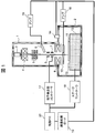
- FIG. 1 shows an apparatus configuration of a scanning electron microscope used in this embodiment.
- the main body of the scanning electron microscope includes a column 1 and a sample chamber 2.
- an electron gun 3 that generates irradiation electrons
- a condenser lens 4 and an objective lens 8 that converge irradiation electrons irradiated on the wafer 11
- a deflector 7 that scans the irradiation electrons with respect to the wafer 11, and irradiation electrons.
- Aligner 5 with respect to the objective lens 8 a secondary electron detector 9 for detecting secondary electrons generated from the wafer 11, and an ExB filter 6 for taking secondary electrons into the secondary electron detector 9.
- a backscattered electron detector 10 for detecting backscattered electrons from the wafer 11 is provided.
- the deflector 7 scans the wafer 11 with irradiation electrons according to a signal given from the electron beam scanning controller 17.
- the XY stage 13 installed in the sample chamber 2 moves the wafer 11 with respect to the column 1 in accordance with a signal given from the stage controller 18.
- a standard sample 12 used for calibration of the incident angle of irradiation electrons is attached on the XY stage 13.
- the apparatus also has an optical microscope 14 for wafer alignment.
- the detection signals output from the secondary electron detector 9 and the backscattered electron detector 10 are converted into signals by the amplifiers 15 and 16 and supplied to the image processing board 19.
- the image processing board 19 adds each signal provided from the secondary electron detector 9 and the backscattered electron detector 10 to form an image.
- the detection signal of the secondary electron detector 9 mainly indicates pattern information on the wafer surface (upper layer), and the detection signal of the reflected electron detector 10 mainly indicates pattern information on the lower layer.
- the image processing board 19 calculates a pattern overlay error as a numerical value from a pattern image generated based on these two detection signals.
- the control PC 20 controls the operation of the entire scanning electron microscope.
- a monitor and an input device (not shown) are connected to the control PC 20.
- a GUI described later is displayed on a monitor (not shown).
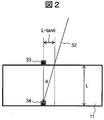
- a pattern 33 and a pattern 34 are formed at the same position of two layers having different heights by the thickness L of the sample 11.
- the shift amount between the pattern 33 and the pattern 34 should be measured as zero.
- the measurement is performed such that the positions of the irradiation electrons 32 are shifted by L ⁇ tan ⁇ . For this reason, it is necessary to calibrate so that the irradiation electrons 32 are incident on the wafer 11 perpendicularly before measuring the overlay deviation amount of the patterns formed in different layers.
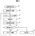
- FIG. 3 shows a procedure for calibrating the inclination (incident angle ⁇ ) of the irradiation electrons 32.
- the operation shown in FIG. 3 is started by selecting a calibration operation for the incident angle of the irradiation electrons 32 on the GUI screen of the monitor (process 41).
- the control PC 20 controls the movement of the XY stage 13 and moves the standard sample 12 to the irradiation region of the irradiation electrons 32 (process 42).
- the pattern is formed at the same position in the two layers without deviation, or a pattern in which the positional relationship between the two patterns having different layers is known is formed.
- the wobbler and stigma are adjusted (process 43). Thereafter, the control PC 20 acquires an image of the standard sample 12 (process 44). Specifically, a secondary electron image corresponding to the uppermost layer pattern of the standard sample 12 and a reflected electron image corresponding to the second layer pattern are acquired.
- the image processing board 19 calculates the incident angle (tilt) ⁇ of the irradiation electrons 32 (process 45). Specifically, the image processing board 19 calculates the pattern position of the upper layer and the pattern position of the lower layer from the detected image, calculates the difference L ⁇ tan ⁇ between the two pattern positions, and calculates the difference and the known thickness. The incident angle ⁇ is calculated using L.
- the image processing board 19 compares the calculated incident angle ⁇ with a specified value (allowable value) (process 46).
- the control PC 20 adjusts the inclination of the irradiation electrons 32 by the aligner 5 (process 47). Thereafter, the control PC 20 returns the process to the process 43. Thereby, with respect to the adjusted incident angle ⁇ , wobbler and stigma adjustment, image acquisition, and calculation processing of the incident angle (tilt) ⁇ are executed. Since the aligner 5 is composed of two sets of alignment coils arranged above and below the column 1, it is possible to change only the inclination of the electron beam while keeping the irradiation position of the irradiation electrons 32 on the sample constant. it can.
- control PC 20 ends the calibration process of the incident angle ⁇ (process 48).
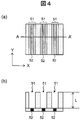
- FIG. 4 is a schematic diagram for explaining the pattern shape formed on the standard sample 12.
- FIG. 4A is a diagram (plan view) of the standard sample 12 viewed from the incident direction of the irradiation electrons 32.
- FIG. 4B is a schematic diagram (cross-sectional view) showing a cross section taken along the line AA ′ in FIG.
- a groove 51 having a depth L is formed on the surface of the standard sample 12, and a line pattern 52 is formed on the bottom surface of the groove 51.
- the groove 51 and the line pattern 52 are formed so that their centers coincide with each other, and it is confirmed by cross-sectional observation of the same lot product that there is no deviation between the centers.
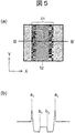
- FIG. 5 shows an SEM image of the standard sample 12.
- the SEM image in FIG. 5A is an image obtained by adding signals from the secondary electron detector 9 and the reflected electron detector 10.
- FIG. 5B shows the signal intensity between B and B '.
- a1 and a2 are signal peaks obtained with respect to the edge of the groove 51. Between b1-b2, it corresponds to the line pattern 52 of the lower layer. The signal intensity between b1 and b2 is higher than the surroundings.
- ⁇ x obtained here is an inclination angle in the X direction, but the inclination angle in the Y direction can be similarly measured for a pattern in which the grooves 51 are formed in the X direction.
- FIG. 6 shows a processing procedure executed when calculating the overlay deviation amount.
- the control PC 20 receives selection of the wafer 11 and recipe and execution of overlay measurement through the GUI screen (process 61).
- the control PC 20 loads the selected wafer 11 into the sample chamber 2 (process 62).
- control PC 20 executes alignment based on the optical microscope image and the SEM image (process 63). Thereafter, the control PC 20 controls the XY stage 13 to move the wafer 11 to the overlay measurement point registered in the recipe (process 64).
- the image processing board 19 acquires an SEM image according to a predetermined condition registered in the recipe (process 65).
- the image processing board 19 detects the pattern position of the upper layer in the secondary electron image based on the signal from the secondary electron detector 9 and the pattern position of the lower layer in the reflected electron image based on the signal from the reflected electron detector 10,
- the overlay deviation amount is calculated from the pattern position difference between the upper layer and the lower layer (process 66).
- the calculation here is performed by subtracting a deviation amount inherent to the incident angle ⁇ of the irradiation electrons 32 from the apparent overlay deviation amount of the upper layer pattern and the lower layer pattern. Details of the calculation method will be described later.
- the control PC 20 determines whether or not the calculation of the overlay deviation amount has been completed for all the measurement points specified in the recipe (process 67). While the measurement point remains (while a negative result is obtained), the control PC 20 moves the next measurement point to the irradiation range of the irradiation electrons 32, and acquires an image and calculates the overlay deviation amount. When measurement is completed for all measurement points (when a positive result is obtained), the control PC 20 unloads the wafer 11 (process 68) and outputs a measurement result of the overlay deviation amount (process 69).
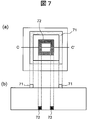
- FIG. 7 shows a structural example of a pattern for measuring the overlay displacement amount.
- FIG. 7A is a view as seen from the incident direction of the irradiation electrons 32, and FIG. 7B shows a C-C 'cross section.
- the pattern 71 is a pattern formed on the wafer surface, and the pattern 72 is a pattern formed inside the wafer. Note that the pattern 71 and the pattern 72 are designed so that their centers coincide.
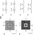
- FIG. 8A is an image obtained from the detection signal output from the secondary electron detector 9, and the peak of the detection signal appears at the edge portion of the pattern 71 formed on the wafer surface.
- FIG. 8B shows the signal intensity between Ax and Ax ′, and four peaks a X1 , a X2 , a X3 , and a X4 are seen corresponding to the pattern edges.
- the center position in the X direction of the pattern 71 is a xc
- the center position a xc is given by the following equation.
- a xc (a X1 + a X2 + a X3 + a X4 ) / 4 (Formula 3)
- a Yc (a Y1 + a Y2 + a Y3 + a Y4 ) / 4 (Formula 4)
- FIG. 8D is an image obtained from the detection signal output from the backscattered electron detector 10, and the signal intensity is strong due to the contrast due to the difference in the material in the pattern 72 formed inside the wafer.
- FIG. 8E shows the signal intensity between Bx and Bx ′, and b X1 , b X2 , b X3 , and b X4 indicate locations where the signal intensity changes.
- the center position b xc of the pattern 72 in the X direction is given by the following equation.
- b xc (b X1 + b X2 + b X3 + b X4 ) / 4 (Formula 5)
- ⁇ x and ⁇ y can be used as a result of the overlay deviation amount measurement. If correction of the amount of deviation due to the incident angle ⁇ of the irradiation electrons 32 is necessary (when a more accurate result is required), the value acquired and held in the calibration process of the incident angle ⁇ of the irradiation electrons 32 Is used to correct the shift amount.
- one electron gun 3, a secondary electron detector 9, and a reflected electron detector 10 are mounted on a scanning electron microscope, and are formed in a pattern formed in an upper layer and a lower layer of measurement points.
- a method is employed in which detection signals corresponding to the formed patterns are simultaneously acquired, and an overlay deviation amount between different layers is calculated.
- the detection signal corresponding to the pattern formed in the upper layer and the detection signal corresponding to the pattern formed in the lower layer can be simultaneously acquired using the same irradiation electron 32, high position detection accuracy can be expected.
- the apparatus configuration can be reduced in size.
- the secondary electron detector 9 is used for the measurement of the pattern formed in the upper layer and the reflected electron detector 10 is used for the measurement of the pattern formed in the lower layer.
- the pattern can be detected with high accuracy.
- the operation of measuring the overlay deviation amount is executed. For this reason, the intrinsic
- the measurement accuracy can be further improved by correcting the overlay deviation amount using the inherent deviation amount caused by the incident angle ⁇ acquired at the time of calibration.
- the calibration of the incident angle ⁇ of the irradiated electrons 32 is performed before the measurement of the overlay deviation amount is started, thereby guaranteeing the accuracy of the overlay deviation measurement performed thereafter.
- the incident angle ⁇ of the irradiation electron 32 is measured. If ⁇ is different before and after the measurement, or if the incident angle ⁇ after the measurement exceeds the specified value, an alarm may be issued. good.
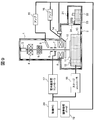
- FIG. 9 shows an apparatus configuration of a scanning electron microscope used in the second embodiment.
- parts corresponding to those in FIG. In addition to the column 1 and the sample chamber 2, a load chamber 21 is disposed in the main body of the scanning electron microscope according to the present embodiment.
- the load chamber 21 is disposed adjacent to the sample chamber 2, and a valve 24 that can be opened and closed is disposed between the sample chambers 2.
- a vacuum aligner 22 and a robot 23 are set in the load chamber 21. It also has a vacuum exhaust mechanism (not shown).
- the robot 23 is a transfer mechanism that moves the wafer 11 between the XY stage 13 and the vacuum aligner 22.
- the vacuum aligner 22 is a rotation mechanism that rotates the wafer 11 in a horizontal plane.
- the vacuum aligner 22 for example, a mechanism described in Patent Document 5 is used.
- the vacuum aligner 22 has a stage on which the wafer 11 is placed, a mechanism for detecting the center position and orientation of the wafer 11, a mechanism for rotationally driving the stage, a mechanism for detecting the rotation amount, and the like.
- the rotation angle is arbitrary, and may be 180 °, 120 °, or 90 °, for example. In the following description, a case where the orientation of the wafer 11 is rotated by 180 ° will be described.
- the wafer 11 remains in the same vacuum state as that of the sample chamber 2 (that is, without being once put out to the external space), and its direction is changed and returned onto the stage 13. be able to.
- the control PC 20 accepts selection of the wafer 11 and recipe and execution of overlay measurement through the GUI screen (process 101).
- the control PC 20 loads the selected wafer 11 into the sample chamber 2 (process 102).
- control PC 20 executes alignment based on the optical microscope image and the SEM image (process 103). Thereafter, the control PC 20 controls the XY stage 13 to move the wafer 11 to the overlay measurement point registered in the recipe (process 104).
- the image processing board 19 acquires an SEM image according to a predetermined condition registered in the recipe (process 105).
- the SEM image here is also obtained by adding signals from the secondary electron detector 9 and the backscattered electron detector 10.
- the image processing board 19 calculates an overlay deviation amount for the acquired SEM image (process 106).
- the calculated overlay deviation amount includes the apparent overlay deviation amount between the upper layer pattern and the lower layer pattern (deviation amount inherent to the incident angle ⁇ of the irradiation electrons 32). ing.
- the calibration process of the incident angle ⁇ described in the first embodiment is basically unnecessary. However, calibration processing may be performed.
- the control PC 20 determines whether or not the calculation of the overlay deviation amount has been completed for all the measurement points specified in the recipe (process 107). While the measurement point remains (while a negative result is obtained), the control PC 20 moves the next measurement point to the irradiation range of the irradiation electrons 32, and acquires an image and calculates the overlay deviation amount.
- control PC 20 moves the wafer 11 to the load chamber 21 and rotates the direction of the wafer 11 by 180 degrees (process 108). Thereafter, the control PC 20 returns the rotated wafer 11 onto the XY stage 13 again.
- control PC 20 executes alignment using the optical microscope image and the SEM image (process 109). Thereafter, the control PC 20 controls the XY stage 13 to move the wafer 11 to the overlay measurement point registered in the recipe (process 110).
- the image processing board 19 acquires an SEM image according to a predetermined condition registered in the recipe (process 111).
- the SEM image here is also obtained by adding signals from the secondary electron detector 9 and the backscattered electron detector 10. Further, the image processing board 19 calculates an overlay deviation amount for the acquired SEM image (process 112).
- the overlay deviation amount here also includes an apparent overlay deviation amount between the upper layer pattern and the lower layer pattern (a deviation amount inherent to the incident angle ⁇ of the irradiation electrons 32).
- control PC 20 determines whether or not the calculation of the overlay deviation amount has been completed for all the measurement points specified in the recipe (process 113).
- control PC 20 unloads the wafer 11 (process 114).
- the image processing board 19 or the control PC 20 corrects the measurement result by using the two overlay displacement amounts measured by changing the direction of one measurement point (process 115). Specifically, the average value of the two overlay deviation amounts is calculated. The process 115 may be executed before unloading the wafer 11 or may be executed simultaneously. Thereafter, the control PC 20 outputs the measurement result of the overlay deviation amount (process 116).
- the orientation of the wafer 11 is rotated by 180 °, and the overlay displacement amount is measured twice from different rotation directions at one measurement point, thereby canceling the displacement amount inherent to the incident angle ⁇ of the irradiation electrons 32.
- the overlay displacement amount is measured twice from different rotation directions at one measurement point, thereby canceling the displacement amount inherent to the incident angle ⁇ of the irradiation electrons 32.
- FIG. 11A shows a state before the wafer 11 is rotated
- FIG. 11B shows a state after the wafer 11 is rotated 180 °.
- a pattern 123 is formed on the upper layer of the wafer 11 and a pattern 124 is formed on the lower layer. Further, it is assumed that the upper layer and the lower layer are different in height by a thickness L. Further, it is assumed that the pattern 123 and the pattern 124 are formed by being shifted by a distance D in the X direction. Further, consider a case where the irradiation electrons 32 are incident on the wafer 11 at an incident angle ⁇ .
- delta 1 from D is the value to be measured originally a value that includes the amount of deviation of + L ⁇ tan ⁇ .
- ⁇ 2 is a value including a deviation amount of ⁇ L ⁇ tan ⁇ from D that should be measured originally.
- the true overlay deviation amount D can be calculated by applying the same processing procedure to the measurement of the overlay deviation amount D in the Y direction.
- the rotation angle of the wafer 11 is arbitrary. For example, the wafer 11 is rotated by 120 ° to measure the overlay deviation amount from three directions at one measurement point, and then the average value of these is calculated. May be. Further, for example, the overlay displacement amount may be measured from four directions at one measurement point by rotating by 90 °, and then the average value of these may be calculated.
- the wafer 11 can be rotated in a vacuum state.
- the working time can be significantly reduced as compared with the case where the wafer 11 is rotated by taking it out from the sample chamber 2.
- the load chamber 21 is provided.
- the load chamber 21 may not be provided. In this case, the apparatus configuration can be further reduced in size.
- this invention is not limited to the Example mentioned above, Various modifications are included.
- the case where the electron gun 3 is used has been described, but an ion source or other charged particle source may be used. That is, not only a scanning electron microscope but also an ion microscope or other charged particle beam apparatus may be used.
- the scanning electron microscope according to each embodiment is not limited to the length measurement SEM, but may be a review SEM.
- each of the above-described configurations, functions, processing units, processing means, and the like may be partly or entirely realized as, for example, an integrated circuit or other hardware.
- Each of the above-described configurations, functions, and the like may be realized by the processor interpreting and executing a program that realizes each function. That is, it may be realized as software.
- Information such as programs, tables, and files for realizing each function can be stored in a memory, a hard disk, a storage device such as an SSD (Solid State Drive), or a storage medium such as an IC card, an SD card, or a DVD.
- control lines and information lines indicate what is considered necessary for explanation, and do not represent all control lines and information lines necessary for the product. In practice, it can be considered that almost all components are connected to each other.
Landscapes
- Physics & Mathematics (AREA)
- General Physics & Mathematics (AREA)
- Chemical & Material Sciences (AREA)
- Analytical Chemistry (AREA)
- Engineering & Computer Science (AREA)
- Computer Vision & Pattern Recognition (AREA)
- Health & Medical Sciences (AREA)
- Toxicology (AREA)
- Electromagnetism (AREA)
- Length-Measuring Devices Using Wave Or Particle Radiation (AREA)
- Testing Or Measuring Of Semiconductors Or The Like (AREA)
Priority Applications (2)
| Application Number | Priority Date | Filing Date | Title |
|---|---|---|---|
| KR1020157009208A KR101712298B1 (ko) | 2012-10-26 | 2013-10-23 | 하전 입자선 장치 및 중첩 어긋남량 측정 방법 |
| US14/435,203 US9224575B2 (en) | 2012-10-26 | 2013-10-23 | Charged particle beam device and overlay misalignment measurement method |
Applications Claiming Priority (2)
| Application Number | Priority Date | Filing Date | Title |
|---|---|---|---|
| JP2012236901A JP5965819B2 (ja) | 2012-10-26 | 2012-10-26 | 荷電粒子線装置及び重ね合わせずれ量測定方法 |
| JP2012-236901 | 2012-10-26 |
Publications (1)
| Publication Number | Publication Date |
|---|---|
| WO2014065311A1 true WO2014065311A1 (ja) | 2014-05-01 |
Family
ID=50544687
Family Applications (1)
| Application Number | Title | Priority Date | Filing Date |
|---|---|---|---|
| PCT/JP2013/078678 Ceased WO2014065311A1 (ja) | 2012-10-26 | 2013-10-23 | 荷電粒子線装置及び重ね合わせずれ量測定方法 |
Country Status (5)
| Country | Link |
|---|---|
| US (1) | US9224575B2 (enExample) |
| JP (1) | JP5965819B2 (enExample) |
| KR (1) | KR101712298B1 (enExample) |
| TW (1) | TWI498522B (enExample) |
| WO (1) | WO2014065311A1 (enExample) |
Cited By (1)
| Publication number | Priority date | Publication date | Assignee | Title |
|---|---|---|---|---|
| CN115507782A (zh) * | 2017-10-13 | 2022-12-23 | 株式会社日立高新技术 | 图案测量装置及图案测量方法 |
Families Citing this family (17)
| Publication number | Priority date | Publication date | Assignee | Title |
|---|---|---|---|---|
| US9418819B2 (en) * | 2013-09-06 | 2016-08-16 | Kla-Tencor Corporation | Asymmetrical detector design and methodology |
| JP6511193B2 (ja) | 2016-04-13 | 2019-05-15 | 株式会社日立ハイテクノロジーズ | パターン計測装置およびパターン計測方法 |
| WO2017184301A1 (en) * | 2016-04-22 | 2017-10-26 | Applied Materials, Inc. | Method for pecvd overlay improvement |
| JP6850234B2 (ja) * | 2017-09-29 | 2021-03-31 | 株式会社日立ハイテク | 荷電粒子線装置 |
| US10403471B2 (en) * | 2017-11-29 | 2019-09-03 | Asml Netherlands B.V. | Systems and methods for charged particle beam modulation |
| US10473460B2 (en) | 2017-12-11 | 2019-11-12 | Kla-Tencor Corporation | Overlay measurements of overlapping target structures based on symmetry of scanning electron beam signals |
| JP2019164886A (ja) * | 2018-03-19 | 2019-09-26 | 株式会社日立ハイテクノロジーズ | ビーム照射装置 |
| JP7093242B2 (ja) * | 2018-06-27 | 2022-06-29 | 株式会社ニューフレアテクノロジー | 荷電粒子ビーム画像取得装置 |
| JP2020187876A (ja) * | 2019-05-13 | 2020-11-19 | 株式会社日立ハイテク | 荷電粒子線装置 |
| JP2021034163A (ja) * | 2019-08-20 | 2021-03-01 | 株式会社日立ハイテク | 荷電粒子ビームシステム、及び重ね合わせずれ量測定方法 |
| JP7254940B2 (ja) * | 2019-08-23 | 2023-04-10 | 株式会社日立ハイテク | オーバーレイ計測システム及びオーバーレイ計測装置 |
| WO2021038764A1 (ja) * | 2019-08-28 | 2021-03-04 | 株式会社日立ハイテク | 荷電粒子ビームシステム、及び重ね合わせずれ量測定方法 |
| CN113363197B (zh) * | 2019-10-30 | 2023-11-03 | 长江存储科技有限责任公司 | 用于校准粒子束的垂直度的方法以及应用于半导体制造工艺的系统 |
| US11054753B1 (en) * | 2020-04-20 | 2021-07-06 | Applied Materials Israel Ltd. | Overlay monitoring |
| JP2022112137A (ja) | 2021-01-21 | 2022-08-02 | 株式会社日立ハイテク | 荷電粒子ビーム装置 |
| TWI885216B (zh) * | 2021-01-29 | 2025-06-01 | 日商日立高新技術科學股份有限公司 | 試料片移設裝置 |
| WO2024068426A1 (en) * | 2022-09-30 | 2024-04-04 | Asml Netherlands B.V. | Scanning electron microscopy (sem) back-scattering electron (bse) focused target and method |
Citations (3)
| Publication number | Priority date | Publication date | Assignee | Title |
|---|---|---|---|---|
| JP2006286685A (ja) * | 2005-03-31 | 2006-10-19 | Renesas Technology Corp | 半導体集積回路装置の製造方法 |
| JP2008058166A (ja) * | 2006-08-31 | 2008-03-13 | Hitachi High-Technologies Corp | パターンのずれ測定方法、及びパターン測定装置 |
| WO2011099490A1 (ja) * | 2010-02-09 | 2011-08-18 | 株式会社日立ハイテクノロジーズ | パターン検査方法、パターン検査プログラム、電子デバイス検査システム |
Family Cites Families (14)
| Publication number | Priority date | Publication date | Assignee | Title |
|---|---|---|---|---|
| JPH03291880A (ja) | 1990-04-06 | 1991-12-24 | Matsushita Electric Works Ltd | リード線付配線部品の組立方法 |
| JP3101114B2 (ja) | 1993-02-16 | 2000-10-23 | 日本電子株式会社 | 走査電子顕微鏡 |
| JP3291880B2 (ja) | 1993-12-28 | 2002-06-17 | 株式会社日立製作所 | 走査形電子顕微鏡 |
| US5923041A (en) * | 1995-02-03 | 1999-07-13 | Us Commerce | Overlay target and measurement procedure to enable self-correction for wafer-induced tool-induced shift by imaging sensor means |
| JPH11283545A (ja) * | 1998-03-30 | 1999-10-15 | Nikon Corp | 電子画像観察装置 |
| EP2365512A3 (en) * | 2000-06-27 | 2012-01-04 | Ebara Corporation | Inspection system by charged particle beam |
| US20040066517A1 (en) * | 2002-09-05 | 2004-04-08 | Hsu-Ting Huang | Interferometry-based method and apparatus for overlay metrology |
| US7842933B2 (en) * | 2003-10-22 | 2010-11-30 | Applied Materials Israel, Ltd. | System and method for measuring overlay errors |
| US7065737B2 (en) * | 2004-03-01 | 2006-06-20 | Advanced Micro Devices, Inc | Multi-layer overlay measurement and correction technique for IC manufacturing |
| JP2007042929A (ja) | 2005-08-04 | 2007-02-15 | Hitachi High-Tech Control Systems Corp | ロードロック装置とその方法及び半導体製造装置 |
| JP5268532B2 (ja) | 2008-09-30 | 2013-08-21 | 株式会社日立ハイテクノロジーズ | 試料計測方法、及び計測装置 |
| JP2010177500A (ja) * | 2009-01-30 | 2010-08-12 | Hitachi High-Technologies Corp | パターンの重ね合わせ評価方法 |
| JP5425601B2 (ja) | 2009-12-03 | 2014-02-26 | 株式会社日立ハイテクノロジーズ | 荷電粒子線装置およびその画質改善方法 |
| JP5986817B2 (ja) * | 2012-06-15 | 2016-09-06 | 株式会社日立ハイテクノロジーズ | オーバーレイ誤差測定装置、及びコンピュータープログラム |
-
2012
- 2012-10-26 JP JP2012236901A patent/JP5965819B2/ja active Active
-
2013
- 2013-09-26 TW TW102134768A patent/TWI498522B/zh active
- 2013-10-23 KR KR1020157009208A patent/KR101712298B1/ko active Active
- 2013-10-23 US US14/435,203 patent/US9224575B2/en active Active
- 2013-10-23 WO PCT/JP2013/078678 patent/WO2014065311A1/ja not_active Ceased
Patent Citations (3)
| Publication number | Priority date | Publication date | Assignee | Title |
|---|---|---|---|---|
| JP2006286685A (ja) * | 2005-03-31 | 2006-10-19 | Renesas Technology Corp | 半導体集積回路装置の製造方法 |
| JP2008058166A (ja) * | 2006-08-31 | 2008-03-13 | Hitachi High-Technologies Corp | パターンのずれ測定方法、及びパターン測定装置 |
| WO2011099490A1 (ja) * | 2010-02-09 | 2011-08-18 | 株式会社日立ハイテクノロジーズ | パターン検査方法、パターン検査プログラム、電子デバイス検査システム |
Cited By (1)
| Publication number | Priority date | Publication date | Assignee | Title |
|---|---|---|---|---|
| CN115507782A (zh) * | 2017-10-13 | 2022-12-23 | 株式会社日立高新技术 | 图案测量装置及图案测量方法 |
Also Published As
| Publication number | Publication date |
|---|---|
| TWI498522B (zh) | 2015-09-01 |
| KR101712298B1 (ko) | 2017-03-03 |
| US20150287569A1 (en) | 2015-10-08 |
| TW201428232A (zh) | 2014-07-16 |
| JP2014086393A (ja) | 2014-05-12 |
| KR20150054973A (ko) | 2015-05-20 |
| US9224575B2 (en) | 2015-12-29 |
| JP5965819B2 (ja) | 2016-08-10 |
Similar Documents
| Publication | Publication Date | Title |
|---|---|---|
| JP5965819B2 (ja) | 荷電粒子線装置及び重ね合わせずれ量測定方法 | |
| US12174551B2 (en) | Pattern measurement device and pattern measurement method | |
| US9390885B2 (en) | Superposition measuring apparatus, superposition measuring method, and superposition measuring system | |
| KR102422827B1 (ko) | 하전 입자 빔 시스템, 및 중첩 시프트량 측정 방법 | |
| TW201543179A (zh) | 微影設備及方法、和製造物品的方法 | |
| JP7346644B2 (ja) | パターン計測方法、パターン計測装置、およびパターン計測プログラム | |
| US12422386B2 (en) | Pattern measurement device | |
| US20130264479A1 (en) | Method and apparatus for measuring displacement between patterns and scanning electron microscope installing unit for measuring displacement between patterns | |
| KR102765307B1 (ko) | 마스크 검사 장치와 방법, 및 그 검사 방법을 포함한 마스크 제조방법 | |
| JP2013183017A (ja) | 描画装置、基準素子、及び物品製造方法 | |
| JP2016058490A (ja) | リソグラフィ装置、および物品の製造方法 |
Legal Events
| Date | Code | Title | Description |
|---|---|---|---|
| 121 | Ep: the epo has been informed by wipo that ep was designated in this application |
Ref document number: 13848287 Country of ref document: EP Kind code of ref document: A1 |
|
| ENP | Entry into the national phase |
Ref document number: 20157009208 Country of ref document: KR Kind code of ref document: A |
|
| WWE | Wipo information: entry into national phase |
Ref document number: 14435203 Country of ref document: US |
|
| NENP | Non-entry into the national phase |
Ref country code: DE |
|
| 122 | Ep: pct application non-entry in european phase |
Ref document number: 13848287 Country of ref document: EP Kind code of ref document: A1 |