WO2014061353A1 - 基板処理装置 - Google Patents
基板処理装置 Download PDFInfo
- Publication number
- WO2014061353A1 WO2014061353A1 PCT/JP2013/073195 JP2013073195W WO2014061353A1 WO 2014061353 A1 WO2014061353 A1 WO 2014061353A1 JP 2013073195 W JP2013073195 W JP 2013073195W WO 2014061353 A1 WO2014061353 A1 WO 2014061353A1
- Authority
- WO
- WIPO (PCT)
- Prior art keywords
- substrate
- heater
- wafer
- processing apparatus
- temperature
- Prior art date
- Legal status (The legal status is an assumption and is not a legal conclusion. Google has not performed a legal analysis and makes no representation as to the accuracy of the status listed.)
- Ceased
Links
Images


Classifications
-
- H—ELECTRICITY
- H01—ELECTRIC ELEMENTS
- H01L—SEMICONDUCTOR DEVICES NOT COVERED BY CLASS H10
- H01L21/00—Processes or apparatus adapted for the manufacture or treatment of semiconductor or solid state devices or of parts thereof
- H01L21/02—Manufacture or treatment of semiconductor devices or of parts thereof
- H01L21/04—Manufacture or treatment of semiconductor devices or of parts thereof the devices having potential barriers, e.g. a PN junction, depletion layer or carrier concentration layer
- H01L21/18—Manufacture or treatment of semiconductor devices or of parts thereof the devices having potential barriers, e.g. a PN junction, depletion layer or carrier concentration layer the devices having semiconductor bodies comprising elements of Group IV of the Periodic Table or AIIIBV compounds with or without impurities, e.g. doping materials
- H01L21/30—Treatment of semiconductor bodies using processes or apparatus not provided for in groups H01L21/20 - H01L21/26
- H01L21/31—Treatment of semiconductor bodies using processes or apparatus not provided for in groups H01L21/20 - H01L21/26 to form insulating layers thereon, e.g. for masking or by using photolithographic techniques; After treatment of these layers; Selection of materials for these layers
- H01L21/3105—After-treatment
- H01L21/311—Etching the insulating layers by chemical or physical means
- H01L21/31127—Etching organic layers
- H01L21/31133—Etching organic layers by chemical means
- H01L21/31138—Etching organic layers by chemical means by dry-etching
-
- B—PERFORMING OPERATIONS; TRANSPORTING
- B05—SPRAYING OR ATOMISING IN GENERAL; APPLYING FLUENT MATERIALS TO SURFACES, IN GENERAL
- B05C—APPARATUS FOR APPLYING FLUENT MATERIALS TO SURFACES, IN GENERAL
- B05C11/00—Component parts, details or accessories not specifically provided for in groups B05C1/00 - B05C9/00
- B05C11/02—Apparatus for spreading or distributing liquids or other fluent materials already applied to a surface ; Controlling means therefor; Control of the thickness of a coating by spreading or distributing liquids or other fluent materials already applied to the coated surface
- B05C11/08—Spreading liquid or other fluent material by manipulating the work, e.g. tilting
-
- B—PERFORMING OPERATIONS; TRANSPORTING
- B05—SPRAYING OR ATOMISING IN GENERAL; APPLYING FLUENT MATERIALS TO SURFACES, IN GENERAL
- B05C—APPARATUS FOR APPLYING FLUENT MATERIALS TO SURFACES, IN GENERAL
- B05C11/00—Component parts, details or accessories not specifically provided for in groups B05C1/00 - B05C9/00
- B05C11/10—Storage, supply or control of liquid or other fluent material; Recovery of excess liquid or other fluent material
- B05C11/1002—Means for controlling supply, i.e. flow or pressure, of liquid or other fluent material to the applying apparatus, e.g. valves
- B05C11/1015—Means for controlling supply, i.e. flow or pressure, of liquid or other fluent material to the applying apparatus, e.g. valves responsive to a conditions of ambient medium or target, e.g. humidity, temperature ; responsive to position or movement of the coating head relative to the target
-
- B—PERFORMING OPERATIONS; TRANSPORTING
- B05—SPRAYING OR ATOMISING IN GENERAL; APPLYING FLUENT MATERIALS TO SURFACES, IN GENERAL
- B05C—APPARATUS FOR APPLYING FLUENT MATERIALS TO SURFACES, IN GENERAL
- B05C9/00—Apparatus or plant for applying liquid or other fluent material to surfaces by means not covered by any preceding group, or in which the means of applying the liquid or other fluent material is not important
- B05C9/08—Apparatus or plant for applying liquid or other fluent material to surfaces by means not covered by any preceding group, or in which the means of applying the liquid or other fluent material is not important for applying liquid or other fluent material and performing an auxiliary operation
- B05C9/14—Apparatus or plant for applying liquid or other fluent material to surfaces by means not covered by any preceding group, or in which the means of applying the liquid or other fluent material is not important for applying liquid or other fluent material and performing an auxiliary operation the auxiliary operation involving heating or cooling
-
- B—PERFORMING OPERATIONS; TRANSPORTING
- B08—CLEANING
- B08B—CLEANING IN GENERAL; PREVENTION OF FOULING IN GENERAL
- B08B3/00—Cleaning by methods involving the use or presence of liquid or steam
- B08B3/04—Cleaning involving contact with liquid
- B08B3/08—Cleaning involving contact with liquid the liquid having chemical or dissolving effect
-
- H—ELECTRICITY
- H01—ELECTRIC ELEMENTS
- H01L—SEMICONDUCTOR DEVICES NOT COVERED BY CLASS H10
- H01L21/00—Processes or apparatus adapted for the manufacture or treatment of semiconductor or solid state devices or of parts thereof
- H01L21/67—Apparatus specially adapted for handling semiconductor or electric solid state devices during manufacture or treatment thereof; Apparatus specially adapted for handling wafers during manufacture or treatment of semiconductor or electric solid state devices or components ; Apparatus not specifically provided for elsewhere
- H01L21/67005—Apparatus not specifically provided for elsewhere
- H01L21/67011—Apparatus for manufacture or treatment
- H01L21/67017—Apparatus for fluid treatment
- H01L21/67028—Apparatus for fluid treatment for cleaning followed by drying, rinsing, stripping, blasting or the like
- H01L21/67034—Apparatus for fluid treatment for cleaning followed by drying, rinsing, stripping, blasting or the like for drying
-
- H—ELECTRICITY
- H01—ELECTRIC ELEMENTS
- H01L—SEMICONDUCTOR DEVICES NOT COVERED BY CLASS H10
- H01L21/00—Processes or apparatus adapted for the manufacture or treatment of semiconductor or solid state devices or of parts thereof
- H01L21/67—Apparatus specially adapted for handling semiconductor or electric solid state devices during manufacture or treatment thereof; Apparatus specially adapted for handling wafers during manufacture or treatment of semiconductor or electric solid state devices or components ; Apparatus not specifically provided for elsewhere
- H01L21/67005—Apparatus not specifically provided for elsewhere
- H01L21/67011—Apparatus for manufacture or treatment
- H01L21/67017—Apparatus for fluid treatment
- H01L21/67028—Apparatus for fluid treatment for cleaning followed by drying, rinsing, stripping, blasting or the like
- H01L21/6704—Apparatus for fluid treatment for cleaning followed by drying, rinsing, stripping, blasting or the like for wet cleaning or washing
- H01L21/67051—Apparatus for fluid treatment for cleaning followed by drying, rinsing, stripping, blasting or the like for wet cleaning or washing using mainly spraying means, e.g. nozzles
-
- H—ELECTRICITY
- H01—ELECTRIC ELEMENTS
- H01L—SEMICONDUCTOR DEVICES NOT COVERED BY CLASS H10
- H01L21/00—Processes or apparatus adapted for the manufacture or treatment of semiconductor or solid state devices or of parts thereof
- H01L21/67—Apparatus specially adapted for handling semiconductor or electric solid state devices during manufacture or treatment thereof; Apparatus specially adapted for handling wafers during manufacture or treatment of semiconductor or electric solid state devices or components ; Apparatus not specifically provided for elsewhere
- H01L21/67005—Apparatus not specifically provided for elsewhere
- H01L21/67011—Apparatus for manufacture or treatment
- H01L21/67098—Apparatus for thermal treatment
- H01L21/67109—Apparatus for thermal treatment mainly by convection
-
- G—PHYSICS
- G03—PHOTOGRAPHY; CINEMATOGRAPHY; ANALOGOUS TECHNIQUES USING WAVES OTHER THAN OPTICAL WAVES; ELECTROGRAPHY; HOLOGRAPHY
- G03F—PHOTOMECHANICAL PRODUCTION OF TEXTURED OR PATTERNED SURFACES, e.g. FOR PRINTING, FOR PROCESSING OF SEMICONDUCTOR DEVICES; MATERIALS THEREFOR; ORIGINALS THEREFOR; APPARATUS SPECIALLY ADAPTED THEREFOR
- G03F7/00—Photomechanical, e.g. photolithographic, production of textured or patterned surfaces, e.g. printing surfaces; Materials therefor, e.g. comprising photoresists; Apparatus specially adapted therefor
- G03F7/26—Processing photosensitive materials; Apparatus therefor
- G03F7/42—Stripping or agents therefor
-
- H—ELECTRICITY
- H01—ELECTRIC ELEMENTS
- H01L—SEMICONDUCTOR DEVICES NOT COVERED BY CLASS H10
- H01L21/00—Processes or apparatus adapted for the manufacture or treatment of semiconductor or solid state devices or of parts thereof
- H01L21/02—Manufacture or treatment of semiconductor devices or of parts thereof
- H01L21/04—Manufacture or treatment of semiconductor devices or of parts thereof the devices having potential barriers, e.g. a PN junction, depletion layer or carrier concentration layer
- H01L21/18—Manufacture or treatment of semiconductor devices or of parts thereof the devices having potential barriers, e.g. a PN junction, depletion layer or carrier concentration layer the devices having semiconductor bodies comprising elements of Group IV of the Periodic Table or AIIIBV compounds with or without impurities, e.g. doping materials
- H01L21/30—Treatment of semiconductor bodies using processes or apparatus not provided for in groups H01L21/20 - H01L21/26
- H01L21/31—Treatment of semiconductor bodies using processes or apparatus not provided for in groups H01L21/20 - H01L21/26 to form insulating layers thereon, e.g. for masking or by using photolithographic techniques; After treatment of these layers; Selection of materials for these layers
- H01L21/3105—After-treatment
- H01L21/311—Etching the insulating layers by chemical or physical means
- H01L21/31127—Etching organic layers
- H01L21/31133—Etching organic layers by chemical means
Definitions
- the present invention includes, for example, a semiconductor wafer, a glass substrate for a liquid crystal display device, a substrate for a plasma display, a substrate for FED (Field Emission Display), a substrate for an optical disc, a substrate for a magnetic disc, a substrate for a magneto-optical disc, a substrate for a photomask,
- the present invention relates to a substrate processing apparatus for processing a substrate such as a ceramic substrate or a solar cell substrate.
- a treatment liquid is supplied to the surface of a substrate such as a semiconductor wafer or a glass substrate for a liquid crystal display panel, and the surface of the substrate is washed with the treatment liquid.
- a substrate processing apparatus that performs a single wafer cleaning process that processes substrates one by one, a spin chuck that rotates the substrate while holding the substrate substantially horizontal, and a substrate rotated by the spin chuck And a nozzle for supplying a treatment liquid to the surface.
- the substrate When processing the substrate, the substrate is rotated together with the spin base of the spin chuck. And a chemical
- the chemical solution supplied onto the surface of the substrate receives a centrifugal force due to the rotation of the substrate and flows on the surface of the substrate toward the peripheral edge. As a result, the chemical solution spreads over the entire surface of the substrate, and chemical treatment for the surface of the substrate is achieved.
- a rinsing process is performed to wash away the chemical attached to the substrate with pure water.
- pure water is supplied from the nozzle to the surface of the substrate being rotated by the spin chuck, and the pure water is expanded by receiving the centrifugal force generated by the rotation of the substrate, so that the chemical solution adhering to the surface of the substrate is washed away. It is.
- Patent Document 1 As such a single-wafer type substrate processing apparatus, as disclosed in Patent Document 1 below, a heater is built in a spin base of a spin chuck, and a substrate placed on the spin base is heated to a high temperature by the heater. ing. For this reason, the temperature of the chemical solution in contact with the surface of the substrate is raised, and the processing capability of the chemical solution can be increased. As a result, the processing rate of the chemical processing can be improved.
- the surface temperature of the spin base may be raised to a very high temperature.
- the amount of power supplied to the heater is limited because it is necessary to supply power to the heater built in the rotatable spin base via the rotating electrical contact. Therefore, there is an upper limit on the set temperature of the heater. is there. Therefore, there is a possibility that the substrate cannot be heated to a desired high temperature.
- an object of the present invention is to provide a substrate processing apparatus capable of executing a low temperature treatment immediately after a high temperature treatment using a heater.
- Another object of the present invention is to provide a substrate processing apparatus capable of heating a substrate to a desired high temperature using a heater.
- the present invention is a substrate processing apparatus for processing a substrate using a processing liquid, the substrate holding means for holding the substrate, and the processing for supplying the processing liquid to the surface of the substrate held by the substrate holding means
- a liquid supply means for rotating the substrate held by the substrate holding means; a heater arranged to face the substrate held by the substrate holding means and for heating the substrate; and the heater At least one of the substrate holding member and the heater supporting member so that the heater supporting member supporting the substrate independently of the substrate holding means and the heater and the substrate held by the substrate holding means approach / separate.
- a substrate processing apparatus including a moving means for moving one of them.
- the distance between the heater and the substrate held by the substrate holding means can be changed.
- the substrate is heated to a high temperature by the heater. From this state, the amount of heat applied to the substrate can be reduced by greatly increasing the distance between the heater and the substrate, thereby cooling the substrate. That is, the low temperature treatment can be executed within a short time after the high temperature treatment using the heater.
- the heater since the heater is not supported by the substrate holding means, the heater is stationary without rotating even when the substrate is rotating. That is, it is not necessary to make the heater rotatable, and therefore it is not necessary to supply power to the heater via the rotating electrical contact. Therefore, since the amount of power supplied to the heater is not limited, the substrate can be heated to a desired high temperature.
- the heater has a facing surface facing the substrate held in the substrate holding means in parallel, and heats the substrate by radiant heat of the facing surface.
- the surface is divided into a plurality of opposing regions that can vary the amount of heat generation per unit area.
- the opposed surface of the heater is divided into a plurality of opposed regions, and the temperature of the opposed regions is individually adjusted. Therefore, for example, by adjusting the plurality of facing regions to a uniform temperature, the entire surface of the facing surface can be maintained at a uniform temperature.
- the heat generation amount per unit area of the plurality of opposed regions is set so as to increase as the distance from the rotation axis due to the rotation of the substrate by the substrate rotating means increases.
- the processing liquid when a high-temperature processing liquid is supplied from the processing liquid supply means to the central portion of the substrate surface, the processing liquid is hot immediately after being supplied to the central portion of the substrate surface, but from the central portion of the substrate. In the process of flowing toward the peripheral edge of the substrate, the liquid temperature is lowered. Therefore, on the surface of the substrate, the temperature of the processing liquid is relatively high at the central portion, the temperature of the processing liquid is relatively low at the peripheral portion, and heat exchange between the processing liquid and the surrounding atmosphere, The temperature at the center of the substrate surface is relatively high, and the temperature at the peripheral edge of the substrate surface is relatively low.
- the temperature of the processing liquid can be made equal throughout the substrate. Thereby, it is possible to perform uniform processing with the processing liquid over the entire surface of the substrate.
- the plurality of opposed regions may include a circular region centered on the rotation axis and one or a plurality of annular regions surrounding the outer periphery of the circular region.
- At least one of the annular regions is divided into a plurality of divided regions in the circumferential direction, and the plurality of divided regions are provided so that the calorific values per unit area of the facing surface can be made different from each other. It is preferable.
- the opposed surface of the heater is divided into a plurality of opposed regions in the circumferential direction, and the temperature of the opposed regions can be adjusted individually. Thereby, even if it is a case where the opposing surface of a heater enlarges, an opposing surface can be maintained at uniform temperature regarding the circumferential direction.
- the substrate holding means includes a plate-like base portion and a substrate support portion attached to the base portion and supporting the substrate in a state of being separated from the base portion, and the heater includes the base portion, It may be accommodated in a space defined by the substrate supported by the substrate support.
- the heater support portion includes a support rod that is inserted in the thickness direction without contacting the base portion and has one end connected to the heater. .
- the support rod passes through the base portion in the thickness direction without contacting the base portion. Therefore, the heater accommodated in the space between the base portion and the substrate can be supported in a state independent of the substrate holding means. Thereby, support of such a heater is realizable with a comparatively simple structure.
- FIG. 10 is a process diagram for describing a first processing example of a resist removal process performed by the substrate processing apparatus shown in FIG. 1. It is a timing chart for demonstrating the process example of FIG. It is a schematic diagram for demonstrating the process example of FIG.
- FIG. 6D is a schematic diagram for explaining a process following FIG. 6C.
- FIG. 6D is a schematic diagram for explaining a process following FIG. 6F.
- FIG. 6D is a schematic diagram for explaining a step following FIG. 6I.
- FIG. 6 is a timing chart for explaining a second processing example of the resist removal processing executed by the substrate processing apparatus shown in FIG. 1. It is a top view which shows typically the structure of the substrate processing apparatus which concerns on 2nd Embodiment of this invention. It is a top view which shows typically the structure of the substrate processing apparatus which concerns on 3rd Embodiment of this invention. It is a top view which shows typically the structure of the substrate processing apparatus which concerns on 4th Embodiment of this invention.
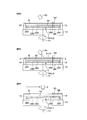
- FIG. 1 is a cross-sectional view schematically showing a configuration of a substrate processing apparatus 1 according to a first embodiment of the present invention.
- the substrate processing apparatus 1 performs an ion implantation process for injecting impurities into the surface (main surface) of a silicon wafer (hereinafter referred to as “wafer”) W as an example of a substrate, or a dry etching process, and then from the surface of the wafer W.
- wafer silicon wafer
- This is a single-wafer type apparatus used in a process for removing an unnecessary resist.
- a substrate processing apparatus 1 includes a spin chuck (substrate holding means) 2 for horizontally holding and rotating a wafer W in a processing chamber 6 partitioned by a partition wall (not shown), and a wafer held by the spin chuck 2.
- a mixture of sulfuric acid and hydrogen peroxide (sulfuric acid / hydrogen) is placed on the lower surface of W and the heater 3 for heating the wafer W from below and the surface (upper surface) of the wafer W held by the spin chuck 2.
- SC1 ammonia-hydrogen peroxide mixture: ammonia
- SC1 ammonia-hydrogen peroxide mixture: ammonia
- SPM liquid peroxide mixture
- a second chemical liquid nozzle (treatment liquid supply means) 5 for supplying a hydrogen peroxide solution mixture.
- the spin chuck 2 for example, a sandwich type is adopted.
- the spin chuck 2 includes a cylindrical rotating shaft 11 extending vertically, a disk-shaped spin base (base portion) 12 attached to the upper end of the rotating shaft 11 in a horizontal posture, and a plurality of spin chucks 12 disposed on the spin base 12. , And a spin motor (substrate rotating means) 14 connected to the rotating shaft 11.
- the spin chuck 2 can hold the wafer W from the periphery by bringing each holding member 13 into contact with the peripheral end surface of the wafer W.
- the first chemical nozzle 4 is, for example, a straight nozzle that discharges the SPM liquid in a continuous flow state.
- the first chemical liquid nozzle 4 is connected to an SPM liquid supply pipe 16 to which a predetermined high temperature (for example, about 160 ° C.) SPM liquid is supplied from an SPM liquid supply source.
- An SPM liquid valve 17 for opening and closing the SPM liquid supply pipe 16 is interposed in the SPM liquid supply pipe 16.
- a first nozzle moving mechanism 18 is coupled to the first chemical liquid nozzle 4.
- the first nozzle moving mechanism 18 is a first chemical solution between a position above the rotation center of the wafer W held on the spin chuck 2 (on the rotation axis A1) and a home position provided at a side position of the spin chuck 2. The nozzle 4 is moved.
- the second chemical liquid nozzle 5 is, for example, a straight nozzle that discharges SC1 in a continuous flow state.
- An SC1 supply pipe 19 to which SC1 from an SC1 supply source whose temperature is adjusted to a predetermined high temperature (for example, about 60 ° C.) is supplied is connected to the second chemical liquid nozzle 5.
- the SC1 supply pipe 19 is provided with an SC1 valve 20 for opening and closing the SC1 supply pipe 19.
- SC1 valve 20 When the SC1 valve 20 is opened, SC1 is supplied from the SC1 supply pipe 19 to the second chemical liquid nozzle 5, and when the SC1 valve 20 is closed, SC1 is supplied from the SC1 supply pipe 19 to the second chemical liquid nozzle 5. Stopped.
- a second nozzle moving mechanism 21 is coupled to the second chemical liquid nozzle 5.
- the second nozzle moving mechanism 21 is located between a position above the rotation center of the wafer W held by the spin chuck 2 (that is, on the rotation axis A1) and a home position provided at a side position of the spin chuck 2. 2 The chemical nozzle 5 is moved.
- the substrate processing apparatus 1 further includes a normal temperature rinsing liquid nozzle (processing liquid supply means) 30 and a high temperature rinsing liquid nozzle (processing liquid supply means) 35.
- the room temperature rinsing liquid nozzle 30 is, for example, a straight nozzle that discharges DIW (deionized water) as an example of a rinsing liquid in a continuous flow state.
- the normal temperature rinsing liquid nozzle 30 discharges DIW at normal temperature (for example, about 25 ° C., the same temperature as the room temperature (RT) of the processing chamber 6).
- the room temperature rinsing liquid nozzle 30 is disposed in a state in which the discharge port faces the center of the upper surface of the wafer W held by the spin chuck 2.
- a room temperature rinse liquid supply pipe 31 Connected to the room temperature rinse liquid nozzle 30 is a room temperature rinse liquid supply pipe 31 to which DIW from a rinse liquid supply source is supplied at room temperature.
- the room temperature rinse liquid supply pipe 31 is provided with a room temperature rinse liquid valve 32 for opening and closing the room temperature rinse liquid supply pipe 31.
- room temperature DIW is supplied from the room temperature rinsing liquid supply pipe 31 to the room temperature rinsing liquid nozzle 30, and room temperature DIW is directed from the room temperature rinsing liquid nozzle 30 toward the center of the upper surface of the wafer W. Discharged.
- the high temperature rinsing liquid nozzle 35 is, for example, a straight nozzle that discharges DIW (deionized water) as an example of the rinsing liquid in a continuous flow state.
- a predetermined high temperature (for example, about 80 ° C.) DIW is discharged from the high temperature rinse liquid nozzle 35.
- the high temperature rinsing liquid nozzle 35 is disposed in a state in which the discharge port faces the center of the upper surface of the wafer W held by the spin chuck 2.
- a high temperature rinsing liquid supply pipe 36 Connected to the high temperature rinsing liquid nozzle 35 is a high temperature rinsing liquid supply pipe 36 which is supplied in a state where DIW from the rinsing liquid supply source is heated to a high temperature.
- the hot rinse liquid supply pipe 36 is provided with a high temperature rinse liquid valve 37 for opening and closing the hot rinse liquid supply pipe 36.
- a high temperature rinse liquid valve 37 for opening and closing the hot rinse liquid supply pipe 36.
- the heater 3 has a disk shape having the same diameter as the wafer W or a slightly smaller diameter than the wafer W, and has a horizontal posture.
- the heater 3 includes a first heater plate 3A concentric with the rotation axis A1, an annular second heater plate 3B surrounding the outer periphery of the first heater plate 3A, and an annular shape surrounding the outer periphery of the second heater plate 3B. And a third heater plate 3C.
- the heater 3 is disposed in a space 39 between the upper surface of the spin base 12 and the lower surface of the wafer W held by the spin chuck 2.
- FIG. 2 is a perspective view showing the configuration of the heater 3. The heater 3 will be described with reference to FIGS. 1 and 2.
- the first heater plate 3A has a disk shape, and a first resistor 28A (see FIG. 1) is built in a ceramic body. On the upper surface of the first heater plate 3A, a horizontal flat first opposing surface (circular region) 29A is formed.
- the second heater plate 3B has an annular plate shape, and a second resistor 28B (see FIG. 1) is built in a ceramic body. On the upper surface of the second heater plate 3B, a horizontal flat annular second opposing surface (annular region) 29B is formed.
- the third heater plate 3C has an annular plate shape, and a third resistor 28C (see FIG. 1) is built in a ceramic body. On the upper surface of the third heater plate 3C, a horizontal flat annular third opposing surface (annular region) 29C is formed.
- the second heater plate 3B is connected and fixed to the first heater plate 3A via a connector (not shown). In the fixed state, there is almost no gap between the inner periphery of the second heater plate 3B and the outer periphery of the first heater plate 3A.
- the third heater plate 3C is connected and fixed to the second heater plate 3B via a connector (not shown). In the fixed state, there is almost no gap between the inner periphery of the third heater plate 3C and the outer periphery of the second heater plate 3B.
- the first to third facing surfaces 29A to 29C are included in the same horizontal plane.
- the first facing surface 29A faces a central region (a circular region having a diameter of about 1/3 of the wafer diameter centered on the rotation center of the wafer W) on the lower surface of the wafer W.
- the second facing surface 29B faces the middle region (the region excluding the central region and the outer peripheral region described below) on the lower surface of the wafer W.
- the third facing surface 29C is opposed to the outer peripheral region (a circle centered on the rotation center of the wafer W and outside the circle having a diameter of about 2/3 of the wafer W diameter) on the lower surface of the wafer W.
- the heater 3 is supported from below by a support rod (heater support member) 25.
- the support rod 25 is inserted in a vertical direction (thickness direction of the spin base 12) along the rotational axis A1 through a through hole 24 that penetrates the spin base 12 and the rotary shaft 11 in the vertical direction.
- the upper end (one end) of the support rod 25 is fixed to the heater 3.
- the lower end (the other end) of the support rod 25 is fixed to a peripheral member below the spin chuck 2, so that the support rod 25 is held in a vertical posture.
- the support rod 25 is not in contact with the spin base 12 or the rotating shaft 11 in the through hole 24, so that the heater 3 is not supported by the spin chuck 2. That is, the heater 3 and the spin chuck 2 are independent of each other. Therefore, even when the spin chuck 2 rotates the wafer W, the heater 3 does not rotate but is stationary (non-rotating state).
- the feed hole 26A to the first resistor 28A, the feed line 26B to the second resistor 28B, and the feed line 26C to the third resistor 28C are inserted into the through hole 24.
- the upper ends of the power supply lines 26A, 26B, and 26C are connected to the first, second, and third resistors 28A, 28B, and 28C, respectively.
- power is supplied to the resistors 28A, 28B, and 28C without using a rotating electrical contact.
- a heater with a rotatable structure it is necessary to supply power to the heater via a rotating electrical contact. In this case, since the rotating electrical contact is interposed, the amount of power supplied to the heater is limited. As a result, the wafer W may not be heated to a desired high temperature.
- the amount of power supply is not limited. Thereby, the wafer W can be heated to a desired high temperature.
- the first resistor 28A generates heat by supplying power to the first resistor 28A, and the first heater plate 3A enters a heat generating state.
- the first facing surface 29A functions as a heat generating surface.
- the power supply to the second resistor 28B causes the second resistor 28B to generate heat, and the second heater plate 3B enters a heat generating state.
- the second facing surface 29B functions as a heat generating surface.
- the third resistor 28C generates heat by supplying power to the third resistor 28C, and the third heater plate 3C enters a heat generating state.
- the third facing surface 29C functions as a heat generating surface.
- the facing surface 29 is configured by the first facing surface 29A, the second facing surface 29B, and the third facing surface 29C.
- power is supplied to the first, second, and third resistors 28A, 28B, and 28C individually, and the amount of power supplied to the resistors 28A, 28B, and 28C is individually controlled. Therefore, the heat generation amount of the first, second and third heater plates 3A, 3B, 3C (surface temperatures of the first opposing surface 29A, the second opposing surface 29B and the third opposing surface 29C) can be individually controlled. .
- a heater elevating mechanism (moving means) 23 for elevating the heater 3 in a horizontal posture is coupled to the support rod 25.
- the heater elevating mechanism 23 is constituted by, for example, a ball screw or a motor.
- the lower surface of the heater 3 has a 0th height position (separated position; see FIG. 6A, etc.) HL0 whose lower surface is separated from the upper surface of the spin base 12 by a predetermined minute distance, and the opposed surface of the heater 3. 29 is moved up and down between the third height position (close position; see FIG. 6B, etc.) HL3 opposed to the lower surface of the wafer W with a minute gap W3.
- interval of the heater 3 and the wafer W can be changed.
- FIG. 3 is a block diagram showing an electrical configuration of the substrate processing apparatus 1.
- the substrate processing apparatus 1 includes a control unit 40 including a microcomputer.
- the control unit 40 controls operations of the spin motor 14 and the first and second nozzle moving mechanisms 18 and 21.
- the control unit 40 controls the amount of heat generated by the heater 3.
- the control unit 40 controls the opening / closing operations of the SPM liquid valve 17, the SC1 valve 20, the room temperature rinse liquid valve 32, and the high temperature rinse liquid valve 37.
- FIG. 4 is a process diagram for explaining a first processing example of the resist removal processing executed by the substrate processing apparatus 1.
- FIG. 5 is a timing chart mainly for explaining the control contents of the control unit 40 in the SPM liquid supply process of step S3 to be described next to the spin dry of step S7.
- 6A to 6J are schematic diagrams for explaining the first processing example. 6A to 6J, the illustration of the configuration below the spin base 12 is omitted.
- the heat generation amount per unit area of the third facing surface 29C is set to the second facing surface 29B.
- the heat generation amount per unit area of the second facing surface 29B is set to be larger than the heat generation amount per unit area of the first facing surface 29A.
- the heat generation amount per unit area of the first to third opposing surfaces 29A, 29B, 29C is set to increase as the distance from the rotation axis A1 increases.
- the temperature TC1 of the third facing surface 29C is set higher than the surface temperature TB1 of the second facing surface 29B, and the surface temperature TB1 of the second facing surface 29B is set to the first facing surface 29A. It is set higher than the surface temperature TA1 (TC1> TB1> TA1).
- the heater 3 When the heater 3 is turned on, the wafer 3 is heated by the heater 3 due to the heater 3 being disposed close to the wafer W.
- a transfer robot (not shown) is controlled, and an unprocessed wafer W is loaded into the process chamber 6 (see FIG. 1) (step S1).
- the wafer W is delivered to the spin chuck 2 with its surface facing upward.
- the heater 3 has already been turned on (driven state), and the height position of the heater 3 is the 0th height level HL0.
- the first and second chemical nozzles 4 and 5 are respectively disposed at the home positions so as not to hinder the loading of the wafer W.
- the heat generation amount per unit area of the first to third opposing surfaces 29A, 29B, and 29C remains a predetermined value. In other words, the output level of the heater 3 does not change.
- the control unit 40 controls the heater lifting mechanism 23 to control the heater lifting mechanism 23 so that the heater 3 is moved to the uppermost third position. Increase to height level HL3.
- the distance W3 between the lower surface of the wafer W held by the spin chuck 2 and the opposed surface 29 of the heater 3 is, for example, 0.5 mm.
- the wafer W held by the spin chuck 2 is heated by radiant heat from the heater 3.
- the first, second, and third opposing surfaces 29A, 29B, and 29C and the lower surface of the wafer W are parallel to each other. Therefore, the amount of heat per unit area given from the heater 3 to the portion of the wafer W facing the third facing surface 29C is larger than the amount of heat per unit area given to the portion of the wafer W facing the second facing surface 29B.
- the amount of heat per unit area given from the heater 3 to the portion of the wafer W facing the second facing surface 29B is larger than the amount of heat per unit area given to the portion of the wafer W facing the first facing surface 29A.
- the amount of heat per unit area given to the wafer W is set to increase as the distance from the rotation axis A1 increases.
- the surface temperature of the wafer W is heated to about 160 ° C. by the heating by the heater 3, although there are variations in various parts of the wafer W.
- control unit 40 controls the first nozzle moving mechanism 18 to move the first chemical solution nozzle 4 above the rotation center of the wafer W.
- the control unit 40 controls the spin motor 14 to start rotating the wafer W (step S2).
- the wafer W is accelerated to a predetermined liquid processing speed (for example, 500-1000 rpm), and then maintained at the liquid processing speed.
- the control unit 40 opens the SPM liquid valve 17 and discharges an SPM liquid of about 160 ° C. from the first chemical liquid nozzle 4, for example.
- the SPM liquid discharged from the first chemical liquid nozzle 4 is supplied to the central portion of the surface of the rotating wafer W (step S3: SPM liquid supply process).
- the SPM liquid supplied to the surface of the wafer W receives centrifugal force due to the rotation of the wafer W and flows on the surface of the wafer W toward the peripheral portion.
- the SPM liquid spreads over the entire surface of the wafer W, and the resist formed on the surface of the wafer W is peeled off by the strong oxidizing power of peroxomonosulfuric acid contained in the SPM liquid.
- the resist peeled from the surface of the wafer W is washed away by the SPM liquid and removed from the surface of the wafer W. Thereby, the reaction between the resist on the surface of the wafer W and the SPM liquid is promoted, and the removal of the resist from the surface of the wafer W proceeds.
- the SPM liquid supplied to the center of the surface of the wafer W exchanges heat with the surrounding atmosphere. Therefore, heat is removed from the wafer W from the SPM liquid in the process of flowing from the central portion toward the peripheral portion on the surface of the wafer W. As a result of heat exchange between the SPM liquid and the wafer W, heat may be taken from the peripheral edge of the wafer W. The amount of heat taken away from the wafer W increases as it goes toward the peripheral edge of the surface of the wafer W.
- a higher amount of heat per unit area is given to the wafer W as it moves away from the rotation axis A1. More specifically, at this time, the first, second and third opposing surfaces 29A, 29B, and 29C are arranged so that the amount of heat deprived from the wafer W from the amount of heat applied to the wafer W becomes uniform at various points on the wafer W at this time.
- the calorific value per unit area is set. As a result, the surface temperature of the wafer W is uniformly distributed at about 160 ° C. throughout the entire area. Thereby, the process by the SPM liquid can be uniformly performed on the entire surface of the wafer W.
- the control unit 40 closes the SPM liquid valve 17 and moves the first chemical liquid nozzle 4 from the rotation center of the wafer W to the home position.
- the control unit 40 controls the heater lifting mechanism 23 to lower the heater 3 to the second height level HL2, which is a lower position than the third height level HL3.
- the distance W2 between the lower surface of the wafer W held by the spin chuck 2 and the opposed surface 29 of the heater 3 is, for example, 10 mm.
- the wafer W held on the spin chuck 2 is heated to about 80 ° C. by the radiant heat from the heater 3, although there are variations in various places. That is, when the heater 3 is lowered, the wafer W that has been about 160 ° C. is cooled.
- the control unit 40 opens the high temperature rinse liquid valve 37 and rotates the wafer W from the discharge port of the high temperature rinse liquid nozzle 35 as shown in FIG. 6E.
- About 80 ° C. DIW is supplied toward the vicinity of the center (step S4: intermediate rinsing step).
- the DIW supplied to the surface of the wafer W receives centrifugal force due to the rotation of the wafer W and flows on the surface of the wafer W toward the peripheral edge of the wafer W. Thereby, the SPM liquid adhering to the surface of the wafer W is washed away by DIW.
- the DIW flows to the peripheral portion of the wafer W without a temperature drop from about 80 ° C.
- the heater 3 does not cool down immediately after being turned off from on. Therefore, if the heater 3 is arranged at the third height level HL3, the heater 3 continues to heat the wafer W with a large amount of heat for a while after the heater 3 is turned off. For this reason, it takes a considerably long time for the temperature of the heater 3 to be sufficiently lowered, and as a result, the processing time of the entire resist removal process may be increased.
- the heating amount to the wafer W is reduced by greatly increasing the interval between the heater 3 and the wafer W from the interval W3 to the interval W2 after the completion of the SPM liquid supply process in step S3. Yes. Thereby, the wafer W can be cooled. As a result, the intermediate rinsing process of step S4 can be started within a short time after the end of the SPM liquid supply process of step S3.
- the hot rinse liquid valve 37 is closed and the supply of DIW to the surface of the wafer W is stopped. Further, as shown in FIG. 6F, the control unit 40 controls the heater lifting mechanism 23 to lower the heater 3 to the first height level HL1, which is a height position lower than the second height level HL2. .
- the interval W1 between the lower surface of the wafer W held by the spin chuck 2 and the opposed surface 29 of the heater 3 is, for example, 20 mm.
- the wafer W held by the spin chuck 2 is heated by radiant heat from the heater 3.
- the first, second and third opposing surfaces 29A, 29B, 29C and the lower surface of the wafer W are parallel to each other. Therefore, the amount of heat per unit area given from the heater 3 to the portion of the wafer W facing the third facing surface 29C is larger than the amount of heat per unit area given to the portion of the wafer W facing the second facing surface 29B.
- the amount of heat per unit area given from the heater 3 to the portion of the wafer W facing the second facing surface 29B is larger than the amount of heat per unit area given to the portion of the wafer W facing the first facing surface 29A. .
- the amount of heat per unit area given to the wafer W is set to increase as the distance from the rotation axis A1 increases. Due to the heating by the heater 3, the surface temperature of the wafer W is heated to about 60 ° C. although there are variations in various parts of the wafer W. That is, as the heater 3 is lowered, the surface temperature of the wafer W is lowered from about 80 ° C. to about 60 ° C. Further, the control unit 40 controls the second nozzle moving mechanism 21 to move the second chemical solution nozzle 5 to a position above the wafer W.
- the control unit 40 opens the SC1 valve 20 and discharges, for example, about 60 ° C. SC1 from the second chemical liquid nozzle 5. Since SC1 has a liquid temperature of about 60 ° C., the processing capacity of SC1 is high. SC1 discharged from the second chemical liquid nozzle 5 is supplied to the central portion of the surface of the rotating wafer W (step S5: SC1 supply process). The SC 1 supplied to the surface of the wafer W receives a centrifugal force due to the rotation of the wafer W and flows on the surface of the wafer W toward the peripheral portion. Thereby, SC1 is supplied uniformly over the entire surface of the wafer W, and foreign substances such as resist residues and particles adhering to the surface of the wafer W can be removed by the chemical ability of SC1.
- the SC1 solution supplied to the center of the surface of the wafer W exchanges heat with the surrounding atmosphere. Therefore, heat is removed from the wafer W from the SC 1 in the process of flowing from the central portion toward the peripheral portion on the surface of the wafer W. As a result of heat exchange between SC1 and wafer W, heat may be taken from the peripheral portion of wafer W. The amount of heat taken away from the wafer W increases as it goes toward the peripheral edge of the surface of the wafer W.
- a higher amount of heat per unit area is given to the wafer W as it moves away from the rotation axis A1. More specifically, at this time, the first, second and third opposing surfaces 29A, 29B, and 29C are arranged so that the amount of heat deprived from the wafer W from the amount of heat applied to the wafer W becomes uniform at various points on the wafer W at this time.
- the calorific value per unit area is set. As a result, the surface temperature of the wafer W is uniformly distributed at about 60 ° C. throughout the entire area. Thereby, the process by SC1 can be uniformly performed to the whole surface of the wafer W.
- the control unit 40 closes the SC1 valve 20. Further, as shown in FIG. 6H, the control unit 40 controls the heater lifting mechanism 23 to lower the heater 3 to the 0th height level HL0 which is a lower position than the first height level HL1. .
- the interval W0 between the lower surface of the wafer W held by the spin chuck 2 and the opposed surface 29 of the heater 3 is, for example, 40 mm. In this state, the distance between the heater 3 and the wafer W held by the spin chuck 2 is excessively wide, so that the radiant heat reaching the wafer W from the heater 3 is small and the influence on the wafer W is small. In other words, the wafer W is not heated by the heater 3. At this time, the surface temperature of the wafer W remains at room temperature.
- the control unit 40 opens the room temperature rinse liquid valve 32 and opens the wafer W from the discharge port of the room temperature rinse liquid nozzle 30 as shown in FIG.
- Room temperature DIW is supplied toward the vicinity of the center of rotation (step S6: final rinse step).
- the DIW supplied to the surface of the wafer W receives centrifugal force due to the rotation of the wafer W and flows on the surface of the wafer W toward the peripheral edge of the wafer W. Thereby, SC1 adhering to the surface of the wafer W is washed away by DIW.
- the DIW is not heated through the wafer W.
- step S7 the spin dry described below (step S7) is executed.
- the control unit 40 controls the heater lifting mechanism 23 so that the heater 3 The height is raised from the zero height level HL0 to the first height level HL1.
- the control unit 40 drives the spin motor 14 to change the rotation speed of the wafer W to a predetermined high rotation speed (for example, 1500 ⁇ (2500 rpm), and spin drying is performed by shaking off the DIW adhering to the wafer W (step S7).
- a predetermined high rotation speed for example, 1500 ⁇ (2500 rpm
- spin drying is performed by shaking off the DIW adhering to the wafer W (step S7).
- the DIW adhering to the wafer W is removed by this spin drying.
- the surface temperature of the wafer W is heated to about 60 ° C. by the radiant heat from the heater 3 at the first height level HL1, although there are variations in various parts of the wafer W. Therefore, DIW adhering to the wafer W is likely to evaporate, thereby reducing the time required for spin drying.
- the control unit 40 drives the spin motor 14 to stop the rotation of the spin chuck 2. Further, the control unit 40 turns off the heater 3 (non-driving state) and controls the heater lifting mechanism 23 to lower the heater 3 to the 0th height level HL0. As a result, the resist removal process for one wafer W is completed, and the processed wafer W is unloaded from the processing chamber 6 by the transfer robot (step S8).
- FIG. 7 is a timing chart for explaining the second processing example. Also in the second processing example, each step shown in FIG. 4 is executed as in the first processing example.
- the second processing example is different from the first processing example in that not only the distance between the heater 3 and the wafer W but also the output level of the heater 3 (the output of each heater plate 3A, 3B, 3C) is different for each process. It is a different point.
- step S ⁇ b> 3 the third output level PL ⁇ b> 3 having the largest amount of heat generation per unit area of the heater 3 is set.
- the heater 3 is at the third height level HL3 as in the first processing example. Due to the heating by the heater 3, the surface temperature of the wafer W is heated to about 160 ° C., although there are variations in various parts of the wafer W.
- the second output level PL2 having the largest amount of heat generation per unit area of the heater 3 is set next to the third output level PL3.
- the heater 3 is at the second height level HL2 as in the first processing example. Due to the heating by the heater 3, the surface temperature of the wafer W is heated to about 80 ° C. although there are variations in various parts of the wafer W.
- the first output level PL1 is set to the first output level PL1 having the second highest heat generation amount per unit area next to the second output level PL2.
- the heater 3 is at the first height level HL1. Due to the heating by the heater 3, the surface temperature of the wafer W is heated to about 60 ° C. although there are variations in various parts of the wafer W.
- step S6 the heater 3 is set to the 0th output level PL0 where no heat is generated.
- the heater 3 is at the 0th height level HL0 as in the first processing example.
- the wafer W is not heated by the heater 3. Therefore, the surface temperature of the wafer W remains at room temperature (for example, about 25 ° C., the same temperature as the room temperature (RT) of the processing chamber 6).
- the amount of heat generated from the heater 3 is so large that the radiant heat from the heater 3 located at the 0th height level HL0 has little influence on the wafer W. It can also be set small.
- heating the wafer W can be stopped while maintaining the heater 3 on by reducing the output level of the heater 3 to the minimum when the wafer W is not heated.
- the heater 3 Once the heater 3 is turned off, it may take a long time to raise the temperature of the heater 3 to a high temperature when the wafer W is reheated.
- the time required for the temperature rise when the wafer W is reheated thereafter can be shortened.
- the amount of heat generated per unit area of the third opposing surface 29C is the amount of heat generated per unit area of the second opposing surface 29B.
- the amount of heat generated per unit area of the second facing surface 29B is set to be larger than the amount of heat generated per unit area of the first facing surface 29A.
- the output level of the heater 3 can be changed gently (over time).
- a broken line in FIG. May be.
- the height position of the heater 3 can be changed simultaneously with the change of the output level of the heater 3.
- the broken line in FIG. It may be changed prior to the change.
- FIG. 8 is a plan view schematically showing the configuration of the substrate processing apparatus 100 according to the second embodiment of the present invention.
- parts corresponding to those shown in the first embodiment are denoted by the same reference numerals as those in FIGS. 1 to 7, and description thereof is omitted.
- the substrate processing apparatus 100 is different from the substrate processing apparatus 1 according to the first embodiment in that a heater 103 is provided instead of the heater 3.
- the heater 103 has a disk shape having substantially the same diameter as the wafer W or slightly smaller than the wafer W, and has a horizontal posture.
- the heater 103 includes a heater plate 101 including a plurality of (for example, four in FIG. 8) divided bodies 102 instead of the third heater plate 3C.
- Each divided body 102 has an arc plate shape and has the same specifications.
- An annular heater plate 101 is formed by combining a plurality (four) of divided bodies 102.
- Each divided body 102 is a resistance-type ceramic heater in which a resistor is built in a ceramic body, similarly to the first heater plate 3A.
- a facing area (divided area) 104 that faces the lower surface of the wafer W held by the spin chuck 2 is formed.
- the facing surface 129 is configured by the plurality of facing regions 104.
- the facing surface 129 of the heater 103 is divided into a plurality of facing regions 104 in the circumferential direction, and the temperature of each facing region 104 is individually adjusted.
- the opposing surface 129 can be kept at a uniform temperature in the circumferential direction. Therefore, the entire area of the facing surface 129 can be kept at a uniform temperature.
- the heater plate 101 is not limited to a configuration divided into a plurality of divided bodies 102, and a configuration in which a plurality of resistors are incorporated in one annular main body and the amount of power supplied to each resistor can be individually controlled is adopted. You can also
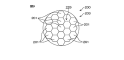
- FIG. 9 is a plan view schematically showing the configuration of the substrate processing apparatus 200 according to the third embodiment of the present invention.
- the difference between the substrate processing apparatus 200 and the substrate processing apparatus 1 according to the first embodiment is that a heater 203 is provided instead of the heater 3.
- the heater 203 has a disc shape having a diameter substantially the same as or slightly smaller than that of the wafer W, and is in a horizontal posture.
- the facing surface 229 of the heater 203 is divided in the radial direction and the circumferential direction, and a large number of ham cam-shaped heater portions 201 are formed.
- Each heater unit 201 has the same specifications.
- Each heater unit 201 is provided with a resistor. Power is supplied to the resistors of each heater unit 201 individually, and the amount of power supplied to each resistor is also individually controlled. Therefore, the amount of heat generated by each heater unit 201 (surface temperature of the heater unit 201) can be individually controlled.
- the facing surface 229 of the heater 203 is divided into a plurality of heater portions 201 in both the circumferential direction and the radial direction, and the temperature of each heater portion 201 is individually adjusted.
- the temperatures (heat generation amounts per unit area) of the plurality of heater units 201 are set to increase as the distance from the rotation axis A1 increases. That is, as in the case of the first embodiment, a temperature distribution is formed on the facing surface 229 so as to increase as the distance from the rotation axis A1 increases.
- the temperature of the processing liquid (SPM liquid, SC1, etc.) flowing on the surface of the wafer W can be made equal throughout the entire surface of the wafer W, and uniform processing with the processing liquid can be performed over the entire surface of the wafer W. it can.
- the temperatures of the heaters 201 are set to a uniform temperature in the circumferential direction. Since each part of the opposing surface 229 is individually controlled to have a uniform temperature in the circumferential direction, the opposing surface 229 can be made uniform in the circumferential direction even when the opposing surface 229 has a large area like the heater 203. Can be kept at temperature.
- the substrate holding means is not limited to a configuration having a spin base such as a spin base.
- FIG. 10 is a cross-sectional view schematically showing a configuration of a substrate processing apparatus 300 according to the fourth embodiment of the present invention.
- the substrate processing apparatus 300 is mainly different from the substrate processing apparatus 1 according to the first embodiment in that a spin chuck (substrate holding means) 301 having no spin base is provided as a substrate holding means.
- the substrate processing apparatus 1 is also greatly different in that the spin chuck 301 is accommodated in a sealed chamber 302 having a sealed internal space.
- the spin chuck 301 includes an annular plate-like motor rotor (substrate rotating means) 303 that is provided to be rotatable about a rotation axis A ⁇ b> 1 extending in the vertical direction, and a plurality of (e.g., 6) disposed on the upper surface of the motor rotor 303. And an annular motor stator 305 (substrate rotating means) disposed outside the sealed chamber 302 and surrounding the side of the motor rotor 303.
- the motor stator 305 has an annular shape with the rotation axis A ⁇ b> 1 as the center of rotation, and the inner periphery of the stator 305 is arranged with a small interval from the outer periphery of the rotor 303.
- the motor rotor 303 includes a back yoke 316 and a magnet 317.
- the back yoke 316 is a magnetic component for preventing magnetic flux leakage and maximizing the magnetic force of the magnet 317.
- the back yoke 316 is annular and has a predetermined thickness in the axial direction.
- a plurality of magnets 317 are provided, and are attached to be arranged in the circumferential direction on the outer peripheral surface of the back yoke 316.
- the motor stator 305 is configured by a coil or the like (not shown), and surrounds the motor rotor 303 with an outer peripheral wall of a cup 306 described below interposed therebetween.
- the spin chuck 301 can hold the wafer W from the periphery by bringing the holding members 304 into contact with the peripheral end surface of the wafer W. Then, power is supplied to the motor rotor 303 and the motor stator 305 from a power source (not shown) in a state where the wafer W is held by the plurality of clamping members 304, so that the wafer W together with the motor rotor 303 passes through the center of the wafer W. It rotates around a vertical rotation axis A1.
- the sealed chamber 302 is configured by combining a bottomed cylindrical cup 306 that houses the spin chuck 301 and a lid member 308 that closes the upper opening 307 of the cup 306.
- the motor rotor 303 and the pinching member 304 of the spin chuck 301 are accommodated and arranged.
- the motor rotor 303 is arranged in a position close to both the bottom wall of the cup 306 and the outer peripheral wall of the cup 306. Yes.
- the lid member 308 has a bottomed cylindrical shape with the opening facing downward.
- a processing liquid nozzle (processing liquid supply means) 309 is inserted into the lid member 308 at a position on the rotation axis A1 of the wafer W.
- the treatment liquid nozzle 309 is supplied with the treatment liquid containing the aforementioned SPM liquid, high temperature DIW, SC1, and DIW, and the treatment liquid is discharged from the discharge port formed at the lower end of the treatment liquid nozzle 309. Yes.
- a seal ring 310 is disposed over the entire periphery.
- the lower end of the outer peripheral wall of the lid member 308 and the upper end of the outer peripheral wall of the cup 306 are abutted with each other with the seal ring 310 interposed therebetween, and are configured by the lid member 308 and the cup 306.
- the sealed chamber 302 is kept in a sealed space.
- the substrate processing apparatus 300 is disposed opposite to the lower surface of the wafer W held by the spin chuck 301, and includes a heater 311 for heating the wafer W from below, a heater base 313 for supporting the heater 311 from below, A heater elevating mechanism (moving means) 312 for elevating and lowering the heater 311 in a horizontal posture is provided.
- the heater 311 is arranged in a region inside the motor rotor 303 in plan view, and has the same configuration as the heater 3 of the first embodiment.
- the heater elevating mechanism 312 is configured by, for example, a ball screw or a motor.
- the heater elevating mechanism 312 is coupled to the heater base 313 and moves the heater 311 up and down together with the heater base 313.
- the heater 311 is driven by the heater elevating mechanism 312 so that the heater 311 has a 0th height position (separation position; see FIG. 6A and the like) HL0 and a third height position. (Proximity position; see FIG. 6B, etc.) It is moved up and down with HL3.
- the height position of the heater 311 includes the 0th height level HL0, the first height level HL1 (see FIG. 6F, etc.), the second height level HL2 (see FIG. 6D, etc.) and the third height. It is switched between levels HL3. That is, the distance between the heater 311 and the wafer W can be changed.
- the wafer 3 when the distance between the heater 311 and the wafer W is narrow, the wafer 3 is heated to a high temperature by the heater 311. From this state, the amount of heat applied to the wafer W can be reduced by greatly increasing the distance between the heater 311 and the wafer W, and the wafer W can be cooled. In addition, the same effects as the effects described in the first embodiment can be achieved.
- the fourth embodiment can be combined with the second embodiment or the third embodiment. That is, instead of the heater 311 of the fourth embodiment, the heater 103 of the second embodiment or the heater 203 of the third embodiment can be employed.
- the heaters 3 and 103 are described as being configured by the plurality of plate heaters 3A, 3B, 3C, and 101.
- the heater has a plurality of resistors on the disk-shaped body.
- a configuration may be employed in which the amount of power supplied to each resistor can be individually controlled.
- the configuration in which the third facing surface 29C is divided is described as an example, but the first facing surface 29A and the second facing surface 29B may be divided.
- the next process (for example, step) is performed.
- the intermediate rinsing process in S6 may be executed.
- resistance-type ceramic heaters have been described as examples.
- infrared heaters such as halogen lamps can be used as the heaters.
- the spin chuck 2 may be raised and lowered. Further, both the heater 3 and the spin chuck 2 may be moved up and down.
- the first chemical liquid nozzle 4 is reciprocated between the rotation center of the wafer W and the peripheral portion, thereby the first chemical liquid
- the supply position on the surface of the wafer W to which the SPM liquid from the nozzle 4 is guided has a circular trajectory intersecting with the rotation direction of the wafer W within the range from the rotation center of the wafer W to the peripheral edge of the wafer W.
- it may be configured to reciprocate. In this case, the SPM liquid can be supplied more uniformly over the entire surface of the wafer W.
- the second chemical liquid nozzle 5 is reciprocated between the rotation center of the wafer W and the peripheral portion, whereby the second chemical liquid nozzle 5, the supply position on the surface of the wafer W to which SC1 is guided is reciprocated in a range from the rotation center of the wafer W to the peripheral edge of the wafer W while drawing an arc-shaped locus intersecting with the rotation direction of the wafer W. It may come to move. In this case, SC1 can be supplied more uniformly over the entire surface of the wafer W.
- first and second chemical liquid nozzles 4 and 5 are fixed nozzles. Form may be sufficient.
- the first and second chemical nozzles 4 and 5 are fixedly arranged above the spin chuck 2 with the discharge port directed toward the center of the upper surface of the wafer W held by the spin chuck 2.
- the case where the resist removal process is performed on the wafer W by using the substrate processing apparatuses 1, 100, 200, and 300 has been described as an example.
- the substrate processing apparatus used for other processes is described in this embodiment.
- the invention can be applied.
- the chemical solution used for the processing is used according to the processing content for the surface of the wafer W.
- SC1 ammonia-hydrogen-peroxide-mixture
- hydrofluoric acid BHF (Bufferd HF), or the like
- BHF Bufferd HF
- a polymer removal solution such as SC1 is used.
- Hydrofluoric acid, SC2 (hydrochloric acid / hydrogen peroxide mixture) or SPM liquid (sulfuric acid / hydrogen peroxide mixture) is used for the cleaning treatment to remove metal contaminants. .
- the rinsing liquid is not limited to DIW, but carbonated water, electrolytic ion water, ozone water, dilution concentration (for example, about 10 to 100 ppm) Hydrochloric acid water, reduced water (hydrogen water), etc. can also be employed as the rinse liquid.
Landscapes
- Engineering & Computer Science (AREA)
- Physics & Mathematics (AREA)
- Condensed Matter Physics & Semiconductors (AREA)
- General Physics & Mathematics (AREA)
- Manufacturing & Machinery (AREA)
- Computer Hardware Design (AREA)
- Microelectronics & Electronic Packaging (AREA)
- Power Engineering (AREA)
- Chemical & Material Sciences (AREA)
- Chemical Kinetics & Catalysis (AREA)
- General Chemical & Material Sciences (AREA)
- Cleaning Or Drying Semiconductors (AREA)
Priority Applications (3)
| Application Number | Priority Date | Filing Date | Title |
|---|---|---|---|
| US14/435,558 US20150258582A1 (en) | 2012-10-16 | 2013-08-29 | Substrate processing device |
| KR1020157012879A KR102132051B1 (ko) | 2012-10-16 | 2013-08-29 | 기판 처리 장치 |
| US15/401,892 US10497581B2 (en) | 2012-10-16 | 2017-01-09 | Substrate processing device |
Applications Claiming Priority (2)
| Application Number | Priority Date | Filing Date | Title |
|---|---|---|---|
| JP2012229139A JP6168273B2 (ja) | 2012-10-16 | 2012-10-16 | 基板処理装置および基板処理方法 |
| JP2012-229139 | 2012-10-16 |
Related Child Applications (2)
| Application Number | Title | Priority Date | Filing Date |
|---|---|---|---|
| US14/435,558 A-371-Of-International US20150258582A1 (en) | 2012-10-16 | 2013-08-29 | Substrate processing device |
| US15/401,892 Continuation US10497581B2 (en) | 2012-10-16 | 2017-01-09 | Substrate processing device |
Publications (1)
| Publication Number | Publication Date |
|---|---|
| WO2014061353A1 true WO2014061353A1 (ja) | 2014-04-24 |
Family
ID=50487930
Family Applications (1)
| Application Number | Title | Priority Date | Filing Date |
|---|---|---|---|
| PCT/JP2013/073195 Ceased WO2014061353A1 (ja) | 2012-10-16 | 2013-08-29 | 基板処理装置 |
Country Status (5)
| Country | Link |
|---|---|
| US (2) | US20150258582A1 (enExample) |
| JP (1) | JP6168273B2 (enExample) |
| KR (1) | KR102132051B1 (enExample) |
| TW (1) | TWI508793B (enExample) |
| WO (1) | WO2014061353A1 (enExample) |
Families Citing this family (21)
| Publication number | Priority date | Publication date | Assignee | Title |
|---|---|---|---|---|
| JP6271304B2 (ja) * | 2013-03-29 | 2018-01-31 | 芝浦メカトロニクス株式会社 | 基板処理装置及び基板処理方法 |
| KR102229786B1 (ko) * | 2014-05-26 | 2021-03-19 | 세메스 주식회사 | 기판 처리 장치 및 기판 처리 방법 |
| KR101919122B1 (ko) * | 2014-08-12 | 2018-11-15 | 주식회사 제우스 | 공정 분리형 기판 처리장치 및 처리방법 |
| KR102343226B1 (ko) * | 2014-09-04 | 2021-12-23 | 삼성전자주식회사 | 스팟 히터 및 이를 이용한 웨이퍼 클리닝 장치 |
| JP6742708B2 (ja) * | 2015-09-29 | 2020-08-19 | 芝浦メカトロニクス株式会社 | 基板処理方法 |
| JP6586697B2 (ja) * | 2015-12-25 | 2019-10-09 | 株式会社Screenホールディングス | 基板処理装置および基板処理方法 |
| JP6689719B2 (ja) * | 2016-09-23 | 2020-04-28 | 株式会社Screenホールディングス | 基板処理装置 |
| JP6947437B2 (ja) * | 2017-03-06 | 2021-10-13 | エーシーエム リサーチ (シャンハイ) インコーポレーテッド | 半導体基板洗浄装置 |
| JP6945314B2 (ja) * | 2017-03-24 | 2021-10-06 | 株式会社Screenホールディングス | 基板処理装置 |
| JP6967922B2 (ja) * | 2017-09-22 | 2021-11-17 | 株式会社Screenホールディングス | 基板処理方法および基板処理装置 |
| KR102030068B1 (ko) | 2017-10-12 | 2019-10-08 | 세메스 주식회사 | 기판 처리 장치 및 기판 처리 방법 |
| JP7004579B2 (ja) * | 2018-01-15 | 2022-01-21 | 東京エレクトロン株式会社 | 基板処理装置、基板処理方法および記憶媒体 |
| JP7263078B2 (ja) * | 2018-09-27 | 2023-04-24 | 東京エレクトロン株式会社 | 基板処理装置および基板処理方法 |
| GB201901637D0 (en) * | 2019-02-06 | 2019-03-27 | Lam Res Ag | Apparatus for processing a wafer, and method of controlling such an apparatus |
| KR102188261B1 (ko) * | 2019-08-02 | 2020-12-09 | 세미기어, 인코포레이션 | 기판 냉각 장치 및 방법 |
| KR102395805B1 (ko) * | 2019-08-26 | 2022-05-11 | 세메스 주식회사 | 기판 처리 장치 및 기판 처리 방법 |
| JP6886546B2 (ja) * | 2020-05-12 | 2021-06-16 | 芝浦メカトロニクス株式会社 | 基板処理装置 |
| US20220390840A1 (en) * | 2021-06-03 | 2022-12-08 | Mks Instruments, Inc. | Light-Enhanced Ozone Wafer Processing System and Method of Use |
| KR102577853B1 (ko) * | 2021-06-22 | 2023-09-13 | 티오에스주식회사 | 기판 처리 장비용 고토크형 매뉴퓰레이터 |
| KR20230102300A (ko) * | 2021-12-30 | 2023-07-07 | 세메스 주식회사 | 기판 처리 장치 및 기판 처리 방법 |
| JP2023125797A (ja) * | 2022-02-28 | 2023-09-07 | 株式会社Screenホールディングス | 基板処理装置および処理カップ洗浄方法 |
Citations (4)
| Publication number | Priority date | Publication date | Assignee | Title |
|---|---|---|---|---|
| JP2005217226A (ja) * | 2004-01-30 | 2005-08-11 | Matsushita Electric Ind Co Ltd | 半導体基板の洗浄方法及び洗浄装置 |
| JP2005277268A (ja) * | 2004-03-26 | 2005-10-06 | Dainippon Screen Mfg Co Ltd | 基板処理装置及び基板処理方法 |
| JP2007173432A (ja) * | 2005-12-21 | 2007-07-05 | Seiko Epson Corp | 半導体基板処理装置及び半導体装置の製造方法 |
| JP2012156264A (ja) * | 2011-01-25 | 2012-08-16 | Tokyo Electron Ltd | 液処理装置および液処理方法 |
Family Cites Families (7)
| Publication number | Priority date | Publication date | Assignee | Title |
|---|---|---|---|---|
| KR100887360B1 (ko) * | 2001-01-23 | 2009-03-06 | 도쿄엘렉트론가부시키가이샤 | 기판처리장치 및 기판처리방법 |
| JP3837026B2 (ja) * | 2001-01-23 | 2006-10-25 | 東京エレクトロン株式会社 | 基板洗浄装置及び基板洗浄方法 |
| TWI343840B (en) * | 2005-07-06 | 2011-06-21 | Applied Materials Inc | Apparatus for electroless deposition of metals onto semiconductor substrates |
| US7914626B2 (en) * | 2005-11-24 | 2011-03-29 | Tokyo Electron Limited | Liquid processing method and liquid processing apparatus |
| JP4787089B2 (ja) | 2006-06-26 | 2011-10-05 | 大日本スクリーン製造株式会社 | 基板処理方法および基板処理装置 |
| US20130087309A1 (en) * | 2011-10-11 | 2013-04-11 | Applied Materials, Inc. | Substrate support with temperature control |
| JP6317547B2 (ja) * | 2012-08-28 | 2018-04-25 | 株式会社Screenホールディングス | 基板処理方法 |
-
2012
- 2012-10-16 JP JP2012229139A patent/JP6168273B2/ja active Active
-
2013
- 2013-08-29 US US14/435,558 patent/US20150258582A1/en not_active Abandoned
- 2013-08-29 KR KR1020157012879A patent/KR102132051B1/ko active Active
- 2013-08-29 WO PCT/JP2013/073195 patent/WO2014061353A1/ja not_active Ceased
- 2013-09-11 TW TW102132773A patent/TWI508793B/zh active
-
2017
- 2017-01-09 US US15/401,892 patent/US10497581B2/en active Active
Patent Citations (4)
| Publication number | Priority date | Publication date | Assignee | Title |
|---|---|---|---|---|
| JP2005217226A (ja) * | 2004-01-30 | 2005-08-11 | Matsushita Electric Ind Co Ltd | 半導体基板の洗浄方法及び洗浄装置 |
| JP2005277268A (ja) * | 2004-03-26 | 2005-10-06 | Dainippon Screen Mfg Co Ltd | 基板処理装置及び基板処理方法 |
| JP2007173432A (ja) * | 2005-12-21 | 2007-07-05 | Seiko Epson Corp | 半導体基板処理装置及び半導体装置の製造方法 |
| JP2012156264A (ja) * | 2011-01-25 | 2012-08-16 | Tokyo Electron Ltd | 液処理装置および液処理方法 |
Also Published As
| Publication number | Publication date |
|---|---|
| TWI508793B (zh) | 2015-11-21 |
| US20170117160A1 (en) | 2017-04-27 |
| TW201420212A (zh) | 2014-06-01 |
| KR20150070354A (ko) | 2015-06-24 |
| JP6168273B2 (ja) | 2017-07-26 |
| US20150258582A1 (en) | 2015-09-17 |
| US10497581B2 (en) | 2019-12-03 |
| JP2014082318A (ja) | 2014-05-08 |
| KR102132051B1 (ko) | 2020-07-08 |
Similar Documents
| Publication | Publication Date | Title |
|---|---|---|
| JP6168273B2 (ja) | 基板処理装置および基板処理方法 | |
| US9601357B2 (en) | Substrate processing device and substrate processing method | |
| JP5615650B2 (ja) | 基板処理方法および基板処理装置 | |
| JP4191009B2 (ja) | 基板処理装置および基板処理方法 | |
| KR102088539B1 (ko) | 기판 처리 방법 및 기판 처리 장치 | |
| JP6222817B2 (ja) | 基板処理方法および基板処理装置 | |
| WO2013140955A1 (ja) | 基板処理装置およびヒータ洗浄方法 | |
| US10405376B2 (en) | Apparatus and method for treating substrate | |
| TW201720542A (zh) | 基板保持旋轉裝置及具備其之基板處理裝置、暨基板處理方法 | |
| JP2009212301A (ja) | 基板処理方法および基板処理装置 | |
| WO2015025889A1 (ja) | 基板処理方法および基板処理装置 | |
| JP2017041512A (ja) | 基板処理方法および基板処理装置 | |
| JP2009267167A (ja) | 基板処理装置 | |
| JP6028892B2 (ja) | 基板処理装置 | |
| JP2015191952A (ja) | 基板処理方法および基板処理装置 | |
| JP5999625B2 (ja) | 基板処理方法 | |
| JP5852927B2 (ja) | 基板処理方法 | |
| JP6191954B2 (ja) | 基板処理方法および基板処理装置 | |
| JP2009105145A (ja) | 基板処理装置 | |
| JP6605655B2 (ja) | 洗浄溶液を製造するための装置及び方法 | |
| JP2013182958A (ja) | 基板処理方法 | |
| JP2014022661A (ja) | 基板処理装置および基板処理方法 |
Legal Events
| Date | Code | Title | Description |
|---|---|---|---|
| 121 | Ep: the epo has been informed by wipo that ep was designated in this application |
Ref document number: 13847208 Country of ref document: EP Kind code of ref document: A1 |
|
| WWE | Wipo information: entry into national phase |
Ref document number: 14435558 Country of ref document: US |
|
| NENP | Non-entry into the national phase |
Ref country code: DE |
|
| ENP | Entry into the national phase |
Ref document number: 20157012879 Country of ref document: KR Kind code of ref document: A |
|
| 122 | Ep: pct application non-entry in european phase |
Ref document number: 13847208 Country of ref document: EP Kind code of ref document: A1 |