WO2014038420A1 - 基板処理方法、コンピュータ記憶媒体及び基板処理システム - Google Patents
基板処理方法、コンピュータ記憶媒体及び基板処理システム Download PDFInfo
- Publication number
- WO2014038420A1 WO2014038420A1 PCT/JP2013/072704 JP2013072704W WO2014038420A1 WO 2014038420 A1 WO2014038420 A1 WO 2014038420A1 JP 2013072704 W JP2013072704 W JP 2013072704W WO 2014038420 A1 WO2014038420 A1 WO 2014038420A1
- Authority
- WO
- WIPO (PCT)
- Prior art keywords
- polymer
- neutral layer
- resist pattern
- substrate processing
- block copolymer
- Prior art date
- Legal status (The legal status is an assumption and is not a legal conclusion. Google has not performed a legal analysis and makes no representation as to the accuracy of the status listed.)
- Ceased
Links
Images


Classifications
-
- H—ELECTRICITY
- H01—ELECTRIC ELEMENTS
- H01L—SEMICONDUCTOR DEVICES NOT COVERED BY CLASS H10
- H01L21/00—Processes or apparatus adapted for the manufacture or treatment of semiconductor or solid state devices or of parts thereof
- H01L21/02—Manufacture or treatment of semiconductor devices or of parts thereof
- H01L21/027—Making masks on semiconductor bodies for further photolithographic processing not provided for in group H01L21/18 or H01L21/34
- H01L21/033—Making masks on semiconductor bodies for further photolithographic processing not provided for in group H01L21/18 or H01L21/34 comprising inorganic layers
- H01L21/0334—Making masks on semiconductor bodies for further photolithographic processing not provided for in group H01L21/18 or H01L21/34 comprising inorganic layers characterised by their size, orientation, disposition, behaviour, shape, in horizontal or vertical plane
- H01L21/0337—Making masks on semiconductor bodies for further photolithographic processing not provided for in group H01L21/18 or H01L21/34 comprising inorganic layers characterised by their size, orientation, disposition, behaviour, shape, in horizontal or vertical plane characterised by the process involved to create the mask, e.g. lift-off masks, sidewalls, or to modify the mask, e.g. pre-treatment, post-treatment
-
- B—PERFORMING OPERATIONS; TRANSPORTING
- B81—MICROSTRUCTURAL TECHNOLOGY
- B81C—PROCESSES OR APPARATUS SPECIALLY ADAPTED FOR THE MANUFACTURE OR TREATMENT OF MICROSTRUCTURAL DEVICES OR SYSTEMS
- B81C1/00—Manufacture or treatment of devices or systems in or on a substrate
- B81C1/00015—Manufacture or treatment of devices or systems in or on a substrate for manufacturing microsystems
- B81C1/00023—Manufacture or treatment of devices or systems in or on a substrate for manufacturing microsystems without movable or flexible elements
- B81C1/00031—Regular or irregular arrays of nanoscale structures, e.g. etch mask layer
-
- G—PHYSICS
- G03—PHOTOGRAPHY; CINEMATOGRAPHY; ANALOGOUS TECHNIQUES USING WAVES OTHER THAN OPTICAL WAVES; ELECTROGRAPHY; HOLOGRAPHY
- G03F—PHOTOMECHANICAL PRODUCTION OF TEXTURED OR PATTERNED SURFACES, e.g. FOR PRINTING, FOR PROCESSING OF SEMICONDUCTOR DEVICES; MATERIALS THEREFOR; ORIGINALS THEREFOR; APPARATUS SPECIALLY ADAPTED THEREFOR
- G03F7/00—Photomechanical, e.g. photolithographic, production of textured or patterned surfaces, e.g. printing surfaces; Materials therefor, e.g. comprising photoresists; Apparatus specially adapted therefor
- G03F7/0002—Lithographic processes using patterning methods other than those involving the exposure to radiation, e.g. by stamping
-
- H—ELECTRICITY
- H01—ELECTRIC ELEMENTS
- H01L—SEMICONDUCTOR DEVICES NOT COVERED BY CLASS H10
- H01L21/00—Processes or apparatus adapted for the manufacture or treatment of semiconductor or solid state devices or of parts thereof
- H01L21/02—Manufacture or treatment of semiconductor devices or of parts thereof
- H01L21/027—Making masks on semiconductor bodies for further photolithographic processing not provided for in group H01L21/18 or H01L21/34
- H01L21/0271—Making masks on semiconductor bodies for further photolithographic processing not provided for in group H01L21/18 or H01L21/34 comprising organic layers
-
- H—ELECTRICITY
- H01—ELECTRIC ELEMENTS
- H01L—SEMICONDUCTOR DEVICES NOT COVERED BY CLASS H10
- H01L21/00—Processes or apparatus adapted for the manufacture or treatment of semiconductor or solid state devices or of parts thereof
- H01L21/67—Apparatus specially adapted for handling semiconductor or electric solid state devices during manufacture or treatment thereof; Apparatus specially adapted for handling wafers during manufacture or treatment of semiconductor or electric solid state devices or components ; Apparatus not specifically provided for elsewhere
- H01L21/67005—Apparatus not specifically provided for elsewhere
- H01L21/67011—Apparatus for manufacture or treatment
- H01L21/67155—Apparatus for manufacturing or treating in a plurality of work-stations
- H01L21/67161—Apparatus for manufacturing or treating in a plurality of work-stations characterized by the layout of the process chambers
- H01L21/67178—Apparatus for manufacturing or treating in a plurality of work-stations characterized by the layout of the process chambers vertical arrangement
-
- B—PERFORMING OPERATIONS; TRANSPORTING
- B81—MICROSTRUCTURAL TECHNOLOGY
- B81C—PROCESSES OR APPARATUS SPECIALLY ADAPTED FOR THE MANUFACTURE OR TREATMENT OF MICROSTRUCTURAL DEVICES OR SYSTEMS
- B81C2201/00—Manufacture or treatment of microstructural devices or systems
- B81C2201/01—Manufacture or treatment of microstructural devices or systems in or on a substrate
- B81C2201/0101—Shaping material; Structuring the bulk substrate or layers on the substrate; Film patterning
- B81C2201/0147—Film patterning
- B81C2201/0149—Forming nanoscale microstructures using auto-arranging or self-assembling material
-
- B—PERFORMING OPERATIONS; TRANSPORTING
- B82—NANOTECHNOLOGY
- B82Y—SPECIFIC USES OR APPLICATIONS OF NANOSTRUCTURES; MEASUREMENT OR ANALYSIS OF NANOSTRUCTURES; MANUFACTURE OR TREATMENT OF NANOSTRUCTURES
- B82Y40/00—Manufacture or treatment of nanostructures
Definitions
- the present invention relates to a substrate processing method, a computer storage medium, and a substrate processing system using a block copolymer including a hydrophilic polymer having hydrophilicity and a hydrophobic polymer having hydrophobicity.
- a resist coating process for coating a resist solution on a semiconductor wafer to form a resist film
- an exposure process for exposing a predetermined pattern on the resist film A photolithography process for sequentially performing a development process for developing the exposed resist film is performed to form a predetermined resist pattern on the wafer.
- an etching process is performed on the film to be processed on the wafer, and then a resist film removing process is performed to form a predetermined pattern on the film to be processed.
- Non-Patent Document 1 a wafer processing method using a block copolymer containing a hydrophilic polymer having hydrophilicity and a hydrophobic polymer having hydrophobicity has been proposed (Non-Patent Document 1).
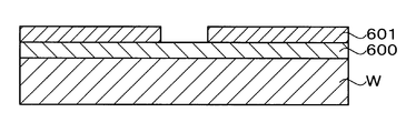
- a resist pattern is first formed on the antireflection film of the wafer, and then a neutral layer having an intermediate affinity for the hydrophilic polymer and the hydrophobic polymer is formed on the antireflection film and the resist pattern. To do. Thereafter, the neutral layer on the resist pattern is removed together with the resist pattern, and a pattern of the neutral layer 601 is formed on the antireflection film 600 of the wafer W as shown in FIG. Thereafter, as shown in FIG.
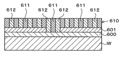
- a block copolymer 610 is applied on the antireflection film 600 and the neutral layer 601, and the hydrophilic polymer 611 and the hydrophobic polymer 612 are phase-separated from the block copolymer 610.
- the antireflection film 600 since the antireflection film 600 has hydrophilicity, on the antireflection film 600, for example, a hydrophobic polymer 612, a hydrophilic polymer 611, and a hydrophobic polymer 612 are separated in this order. Thereafter, for example, the hydrophilic polymer 611 is removed, whereby a fine pattern of the hydrophobic polymer 612 is formed on the wafer W. Then, the film to be processed is etched using the pattern of the hydrophobic polymer 612 as a mask, and a predetermined pattern is formed on the film to be processed.
- Non-Patent Document 1 when the wafer processing method described in Non-Patent Document 1 is used, a portion where the antireflection film 600 is exposed in the neutral layer 601 is recessed on the wafer W as shown in FIG.
- the block copolymer 610 applied on the wafer W as shown in FIG. 29 the height of the pattern of the hydrophilic polymer 611 becomes non-uniform in the wafer surface.
- the etching depth in the wafer surface becomes non-uniform when etching the film to be processed using the pattern of the hydrophobic polymer 612 as a mask. For this reason, the etching process of a to-be-processed film cannot be performed appropriately, and a predetermined pattern may not be appropriately formed in a to-be-processed film.
- the present invention has been made in view of such points, and an object of the present invention is to appropriately form a predetermined pattern on a substrate in substrate processing using a block copolymer containing a hydrophilic polymer and a hydrophobic polymer.
- the present invention provides a method for treating a substrate using a block copolymer comprising a first polymer and a second polymer, wherein the first polymer and the second polymer are processed.
- a neutral layer forming step for forming a neutral layer having an intermediate affinity for the polymer on the substrate, and the substrate on which the resist pattern is formed on the neutral layer, exposed from the resist pattern Applying the block copolymer onto the neutral layer on the neutral layer treatment step for surface-treating the exposed surface of the neutral layer and the substrate from which the resist pattern has been removed after the neutral layer treatment step
- the exposed surface of the neutral layer exposed from the resist pattern is surface-treated, and the surface of the neutral layer is kept flat. If it does so, even if a block copolymer is apply
- Another aspect of the present invention is a readable computer storage medium storing a program that operates on a computer of a control unit that controls the substrate processing system so that the substrate processing method is executed by the substrate processing system.
- the present invention provides a system for processing a substrate using a block copolymer including a first polymer and a second polymer, wherein the first polymer and the second polymer are combined with each other.
- a neutral layer forming apparatus for forming a neutral layer having an intermediate affinity on the substrate, and the neutral layer exposed from the resist pattern with respect to the substrate on which the resist pattern is formed on the neutral layer
- a neutral layer processing apparatus for surface-treating an exposed surface of a layer; and the block copolymer for the substrate from which the resist pattern is removed after the exposed surface is surface-treated by the neutral layer processing apparatus.
- a block copolymer coating device for coating on a neutral layer; a polymer separation device for phase-separating the block copolymer on the neutral layer into the first polymer and the second polymer;
- a predetermined pattern can be appropriately formed on a substrate in substrate processing using a block copolymer containing a hydrophilic polymer and a hydrophobic polymer.
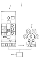
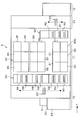
- FIG. 1 is an explanatory diagram showing an outline of a configuration of a substrate processing system 1 according to the present embodiment.
- the substrate processing system 1 includes a coating and developing apparatus 2 that performs photolithography processing on a wafer as a substrate, and an etching processing apparatus 3 that performs etching processing on the wafer.
- a film to be processed (not shown) is formed in advance on the wafer processed by the substrate processing system 1.
- the coating / developing apparatus 2 includes, for example, a cassette station 10 in which a cassette C containing a plurality of wafers W is carried in and out of the outside, and a predetermined type of sheet processing in a photolithography process.
- a processing station 11 having a plurality of various processing apparatuses for processing and an interface station 13 for transferring the wafer W between the exposure apparatus 12 adjacent to the processing station 11 are integrally connected. .
- the cassette station 10 is provided with a cassette mounting table 20.
- the cassette mounting table 20 is provided with a plurality of, for example, four cassette mounting plates 21.
- the cassette mounting plates 21 are arranged in a line in the horizontal X direction (vertical direction in FIG. 2).
- the cassette C can be placed on these cassette placement plates 21 when the cassette C is carried in and out of the coating and developing treatment apparatus 2.
- the cassette station 10 is provided with a wafer transfer device 23 that is movable on a transfer path 22 extending in the X direction.
- the wafer transfer device 23 is also movable in the vertical direction and the vertical axis direction ( ⁇ direction), and includes a cassette C on each cassette mounting plate 21 and a delivery device for a third block G3 of the processing station 11 described later.
- the wafer W can be transferred between the two.
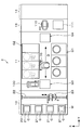
- the processing station 11 is provided with a plurality of, for example, four blocks G1, G2, G3, and G4 having various devices.
- the first block G1 is provided on the front side of the processing station 11 (X direction negative direction side in FIG. 2), and the second side is provided on the back side of the processing station 11 (X direction positive direction side in FIG. 2).
- Block G2 is provided.
- a third block G3 is provided on the cassette station 10 side (Y direction negative direction side in FIG. 1) of the processing station 11, and the interface station 13 side (Y direction positive direction side in FIG. 2) of the processing station 11 is provided. Is provided with a fourth block G4.
- a plurality of liquid processing apparatuses for example, a developing apparatus 30 for developing the wafer W, and a cleaning apparatus 31 for cleaning the wafer W by coating the wafer W with an organic solvent.
- An antireflection film forming device 32 for forming an antireflection film on the wafer W, a neutral layer forming device 33 for applying a neutral agent on the wafer W to form a neutral layer, and a resist solution on the wafer W Then, a resist coating device 34 for forming a resist film and a block copolymer coating device 35 for coating a block copolymer on the wafer W are stacked in order from the bottom.
- the developing device 30, the cleaning device 31, the antireflection film forming device 32, the neutral layer forming device 33, the resist coating device 34, and the block copolymer coating device 35 are arranged side by side in the horizontal direction.
- the number and arrangement of the developing device 30, the cleaning device 31, the antireflection film forming device 32, the neutral layer forming device 33, the resist coating device 34, and the block copolymer coating device 35 can be arbitrarily selected.
- the cleaning device 31, the antireflection film forming device 32, the neutral layer forming device 33, the resist coating device 34, and the block copolymer coating device 35 for example, a spin for applying a predetermined coating solution onto the wafer W. Coating is performed.
- spin coating for example, a coating liquid is discharged onto the wafer W from a coating nozzle, and the wafer W is rotated to diffuse the coating liquid to the surface of the wafer W.
- the block copolymer applied onto the wafer W by the block copolymer coating device 35 includes a first polymer and a second polymer.
- a hydrophobic polymer having hydrophobicity (nonpolar) is used as the first polymer
- a hydrophilic polymer having hydrophilicity (polarity) is used as the second polymer.
- PMMA polymethyl methacrylate
- PS polystyrene
- the ratio of the molecular weight of the hydrophilic polymer in the block copolymer is 40% to 60%, and the ratio of the molecular weight of the hydrophobic polymer in the block copolymer is 60% to 40%.
- the block copolymer is a polymer obtained by linearly combining these hydrophilic polymer and hydrophobic polymer.
- the neutral layer formed on the wafer W by the neutral layer forming apparatus 33 has an intermediate affinity for the hydrophilic polymer and the hydrophobic polymer.
- a random copolymer or an alternating copolymer of polymethyl methacrylate and polystyrene is used as the neutral layer.
- neutral means having an intermediate affinity for the hydrophilic polymer and the hydrophobic polymer.
- a heat treatment apparatus 40 that performs heat treatment of the wafer W, and a neutral layer treatment that performs surface treatment of the neutral layer by irradiating the neutral layer on the wafer W with ultraviolet rays.
- An ultraviolet irradiation device 41 as an apparatus, an adhesion device 42 for hydrophobizing the wafer W, and a peripheral exposure device 43 for exposing the outer periphery of the wafer W are provided side by side in the vertical and horizontal directions.
- the heat treatment apparatus 40 includes a hot plate for placing and heating the wafer W and a cooling plate for placing and cooling the wafer W, and can perform both heat treatment and cooling treatment.
- the ultraviolet irradiation device 41 includes a mounting table on which the wafer W is mounted, and an ultraviolet irradiation unit that irradiates the wafer W on the mounting table with ultraviolet light having a wavelength of 172 nm, for example.
- some of the heat treatment apparatuses 40 are polymers that cause the block copolymer coated on the wafer W by the block copolymer coating apparatus 35 to phase-separate into a hydrophilic polymer and a hydrophobic polymer. Functions as a separation device.
- the number and arrangement of the heat treatment apparatus 40, the ultraviolet irradiation apparatus 41, the adhesion apparatus 42, and the peripheral exposure apparatus 43 can be arbitrarily selected.
- a plurality of delivery devices 50, 51, 52, 53, 54, 55, 56 are provided in order from the bottom.
- the fourth block G4 is provided with a plurality of delivery devices 60, 61, 62 in order from the bottom.
- a wafer transfer area D is formed in an area surrounded by the first block G1 to the fourth block G4.
- a wafer transfer device 70 is disposed in the wafer transfer region D.
- the wafer transfer device 70 has, for example, a transfer arm that is movable in the Y direction, the X direction, the ⁇ direction, and the vertical direction.
- the wafer transfer device 70 moves in the wafer transfer area D and transfers the wafer W to a predetermined device in the surrounding first block G1, second block G2, third block G3, and fourth block G4. it can.
- a plurality of wafer transfer apparatuses 70 are arranged in the vertical direction, and can transfer the wafer W to a predetermined apparatus having the same height of each of the blocks G1 to G4, for example.
- a shuttle transfer device 80 that transfers the wafer W linearly between the third block G3 and the fourth block G4 is provided.
- the shuttle transport device 80 is linearly movable in the Y direction, for example.
- the shuttle transfer device 80 moves in the Y direction while supporting the wafer W, and can transfer the wafer W between the transfer device 52 of the third block G3 and the transfer device 62 of the fourth block G4.
- a wafer transfer device 100 is provided next to the third block G3 on the positive side in the X direction.
- the wafer transfer apparatus 100 has a transfer arm that is movable in the X direction, the ⁇ direction, and the vertical direction, for example.
- the wafer transfer device 100 can move up and down while supporting the wafer W, and can transfer the wafer W to each delivery device in the third block G3.
- the interface station 13 is provided with a wafer transfer device 110 and a delivery device 111.
- the wafer transfer device 110 has a transfer arm that is movable in the Y direction, the ⁇ direction, and the vertical direction, for example.
- the wafer transfer device 110 can transfer the wafer W between each transfer device, the transfer device 111, and the exposure device 12 in the fourth block G4, for example, by supporting the wafer W on a transfer arm.
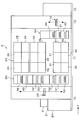
- the etching processing apparatus 3 includes a cassette station 200 that carries the wafer W into and out of the etching processing apparatus 3, a common transport unit 201 that transports the wafer W, and a block copolymer that is phase-separated on the wafer W.
- the cassette station 200 has a transfer chamber 211 in which a wafer transfer mechanism 210 for transferring the wafer W is provided.
- the wafer transfer mechanism 210 has two transfer arms 210a and 210b that hold the wafer W substantially horizontally, and is configured to transfer the wafer W while holding it by either of the transfer arms 210a and 210b.
- a cassette mounting table 212 on which a cassette C capable of accommodating a plurality of wafers W arranged side by side is mounted on the side of the transfer chamber 211. In the illustrated example, a plurality of, for example, three cassettes C can be mounted on the cassette mounting table 212.
- the transfer chamber 211 and the common transfer unit 201 are connected to each other via two load lock devices 213a and 213b that can be evacuated.
- the common transfer unit 201 includes a transfer chamber chamber 214 having a sealable structure formed to have a substantially polygonal shape (in the illustrated example, a hexagonal shape) as viewed from above, for example.
- a wafer transfer mechanism 215 for transferring the wafer W is provided in the transfer chamber 214.
- the wafer transfer mechanism 215 has two transfer arms 215a and 215b that hold the wafer W substantially horizontally, and is configured to transfer the wafer W while holding the wafer W by either of the transfer arms 215a and 215b. .
- Etching devices 202, 203, 204, 205 and load lock devices 213 b, 213 a are arranged outside the transfer chamber chamber 214 so as to surround the periphery of the transfer chamber chamber 214.
- the etching devices 202, 203, 204, 205 and the load lock devices 213b, 213a are arranged in this order in the clockwise direction when viewed from above, for example, and face the six side portions of the transfer chamber 214, respectively. Are arranged.
- an RIE (Reactive Ion Etching) apparatus is used as the etching apparatuses 202 to 205, for example. That is, in the etching apparatuses 202 to 205, dry etching for etching the hydrophobic polymer and the film to be processed is performed by reactive gas (etching gas), ions, and radicals.
- etching gas reactive gas
- ions ions
- radicals radicals
- the substrate processing system 1 described above is provided with a control unit 300 as shown in FIG.
- the control unit 300 is a computer, for example, and has a program storage unit (not shown).
- the program storage unit stores a program for controlling the processing of the wafer W in the substrate processing system 1.
- the program storage unit also stores a program for controlling the operation of driving systems such as the above-described various processing apparatuses and transfer apparatuses to realize a peeling process described later in the substrate processing system 1.
- the program is recorded on a computer-readable storage medium such as a computer-readable hard disk (HD), flexible disk (FD), compact disk (CD), magnetic optical desk (MO), or memory card. Or installed in the control unit 300 from the storage medium.
- HD computer-readable hard disk
- FD flexible disk
- CD compact disk
- MO magnetic optical desk
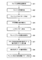
- FIG. 6 is a flowchart showing an example of main steps of such wafer processing.
- a cassette C containing a plurality of wafers W is carried into the cassette station 10 of the coating and developing treatment apparatus 2 and placed on a predetermined cassette placing plate 21. Thereafter, the wafers W in the cassette C are sequentially taken out by the wafer transfer device 23 and transferred to the transfer device 53 of the processing station 11.
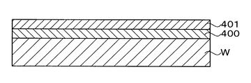
- the wafer W is transferred to the heat treatment apparatus 40 by the wafer transfer apparatus 70 and the temperature is adjusted. Thereafter, the wafer W is transferred to the antireflection film forming apparatus 32 by the wafer transfer apparatus 70, and an antireflection film 400 is formed on the wafer W as shown in FIG. 7 (step S1 in FIG. 6). Thereafter, the wafer W is transferred to the heat treatment apparatus 40, heated, and the temperature is adjusted.
- the wafer W is transferred to the neutral layer forming device 33 by the wafer transfer device 70.
- the neutral layer forming apparatus 33 as shown in FIG. 7, a neutral agent is applied on the antireflection film 400 of the wafer W to form a neutral layer 401 (step S2 in FIG. 6).
- the wafer W is transferred to the heat treatment apparatus 40, heated, temperature-controlled, and then returned to the delivery apparatus 53.
- the wafer W is transferred to the delivery device 54 by the wafer transfer device 100. Thereafter, the wafer W is transferred to the adhesion device 42 by the wafer transfer device 70 and subjected to an adhesion process. Thereafter, the wafer W is transferred to the resist coating device 34 by the wafer transfer device 70, and a resist solution is applied onto the neutral layer 401 of the wafer W to form a resist film. Thereafter, the wafer W is transferred to the heat treatment apparatus 40 by the wafer transfer apparatus 70 and pre-baked. Thereafter, the wafer W is transferred to the delivery device 55 by the wafer transfer device 70.
- the wafer W is transferred to the peripheral exposure device 43 by the wafer transfer device 70 and subjected to peripheral exposure processing. Thereafter, the wafer W is transferred to the delivery device 56 by the wafer transfer device 70.
- the wafer W is transferred to the transfer device 52 by the wafer transfer device 100 and transferred to the transfer device 62 by the shuttle transfer device 80.
- the wafer W is transferred to the exposure apparatus 12 by the wafer transfer apparatus 110 of the interface station 13 and subjected to exposure processing.
- the wafer W is transferred from the exposure apparatus 12 to the delivery apparatus 60 by the wafer transfer apparatus 110. Thereafter, the wafer W is transferred to the heat treatment apparatus 40 by the wafer transfer apparatus 70 and subjected to post-exposure baking. Thereafter, the wafer W is transferred to the developing device 30 by the wafer transfer device 70 and developed. After the development is completed, the wafer W is transferred to the heat treatment apparatus 40 by the wafer transfer apparatus 70 and subjected to a post-bake process.
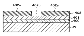
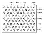
- a predetermined resist pattern 402 is formed on the neutral layer 401 of the wafer W as shown in FIG. 8 (step S3 in FIG. 6). In this embodiment, the resist pattern 402 has a linear shape in plan view.
- the width of the space portion 402b is set so that the hydrophilic polymer 405 and the hydrophobic polymer 406 are alternately arranged in the odd number layers in the space portion 402b as described later.
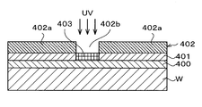
- the wafer W on which the resist pattern 402 is formed is transferred to the ultraviolet irradiation device 41 by the wafer transfer device 70.
- the ultraviolet irradiation device 41 as shown in FIG. 9, the exposed surface of the neutral layer 401 exposed from the resist pattern 402 (space portion 402b) is irradiated with ultraviolet rays. At this time, ultraviolet rays having a wavelength of 172 nm are irradiated. Then, the exposed surface of the neutral layer 401 is oxidized and hydrophilized (step S4 in FIG. 6).
- the region of the neutral layer 401 thus made hydrophilic may be referred to as a hydrophilic region 403.
- the wavelength of ultraviolet rays for forming the hydrophilic region 403 in the neutral layer 401 may be 300 nm or less.
- active oxygen can be generated from oxygen in the processing atmosphere, and the exposed surface of the neutral layer 401 is oxidized and hydrophilized by this active oxygen.
- active oxygen in order to generate
- the wavelength of ultraviolet rays is 172 nm, not only when ozone is used as a processing atmosphere, but also when the processing atmosphere is an air atmosphere, active oxygen can be efficiently generated from oxygen in the air atmosphere. I know it.
- the wafer W is transferred to the cleaning device 31 by the wafer transfer device 70.
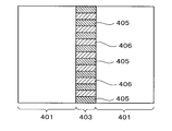
- the cleaning device 31 an organic solvent is supplied onto the wafer W, and the resist pattern 402 on the wafer W is removed as shown in FIG. 10 (step S5 in FIG. 6).
- the neutral layer 401 the surface of the hydrophilic region 403 has hydrophilicity, and the surface of other regions has neutrality. And the surface of the neutral layer 401 is maintained flat.
- the wafer W is transferred to the delivery device 50 by the wafer transfer device 70.
- the wafer W is transferred to the delivery device 55 by the wafer transfer device 100. Thereafter, the wafer W is transferred to the block copolymer coating device 35 by the wafer transfer device 70.
- the block copolymer coating device 35 the block copolymer 404 is coated on the neutral layer 401 of the wafer W as shown in FIG. 11 (step S6 in FIG. 6). At this time, since the surface of the neutral layer 401 is kept flat, the block copolymer 404 is also applied so as to have a uniform film thickness.
- the wafer W is transferred to the heat treatment apparatus 40 by the wafer transfer apparatus 70.
- a heat treatment at a predetermined temperature is performed on the wafer W.
- the block copolymer 404 on the wafer W is phase-separated into the hydrophilic polymer 405 and the hydrophobic polymer 406 (step S7 in FIG. 6).
- the molecular weight ratio of the hydrophilic polymer 405 is 40% to 60%
- the molecular weight ratio of the hydrophobic polymer 406 is 60% to 40%.
- step S6 as shown in FIGS. 12 and 13
- the hydrophilic polymer 405 and the hydrophobic polymer 406 are phase-separated into a lamellar structure.
- the width of the space portion 402b of the resist pattern 402 is formed to a predetermined width in the above-described step S3
- the hydrophilic polymer 405 and the hydrophobic polymer 406 are formed on the hydrophilic region 403 of the neutral layer 401. Alternatingly arranged in odd layers, for example, three layers.
- the hydrophilic polymer 405 is disposed in the middle on the hydrophilic region 403, and the hydrophobic polymers 406 and 406 are disposed on both sides thereof. And the hydrophilic polymer 405 and the hydrophobic polymer 406 are alternately arrange
- the wafer W is transferred to the delivery device 50 by the wafer transfer device 70, and then transferred to the cassette C of the predetermined cassette mounting plate 21 by the wafer transfer device 23 of the cassette station 10.
- the cassette C containing the wafer W is unloaded from the coating and developing treatment apparatus 2 and then loaded into the etching processing apparatus 3.
- one wafer W is taken out from the cassette C on the cassette mounting table 212 by the wafer transfer mechanism 210 and loaded into the load lock apparatus 213 a.
- the inside of the load lock device 213a is sealed and decompressed.
- the inside of the load lock device 213a and the inside of the transfer chamber chamber 214 in a state where the pressure is reduced with respect to the atmospheric pressure (for example, a substantially vacuum state) are communicated.
- the wafer transfer mechanism 215 unloads the wafer W from the load lock device 213a and loads it into the transfer chamber 214.
- the wafer W carried into the transfer chamber 214 is then transferred to the etching apparatus 202 by the wafer transfer mechanism 215.
- the wafer W is etched, and the hydrophilic polymer 405 is selectively removed as shown in FIG. 14 to form a predetermined pattern of the hydrophobic polymer 406 (step S8 in FIG. 6).
- the pattern height of the hydrophobic polymer 406 is also uniform.
- the wafer W is transferred to the etching apparatus 204 by the wafer transfer mechanism 215.
- the film to be processed on the wafer W is etched using the hydrophobic polymer 406 on the wafer W as a mask.
- the hydrophobic polymer 406 and the antireflection film are removed, and a predetermined pattern is formed on the film to be processed (step S9 in FIG. 6).
- the wafer W is returned again into the transfer chamber 214 by the wafer transfer mechanism 215. Then, the wafer is transferred to the wafer transfer mechanism 210 via the load lock device 213b and stored in the cassette C. Thereafter, the cassette C containing the wafers W is unloaded from the etching processing apparatus 3 and a series of wafer processing ends.
- step S4 the exposed surface of the neutral layer 401 exposed from the resist pattern 402 (space portion 402b) is subjected to surface treatment to make it hydrophilic, and the surface of the neutral layer 401 is flattened. Maintained. Then, even if the block copolymer 404 is applied on the neutral layer 401 in the subsequent step S6, the surface of the block copolymer 404 is formed flat. For this reason, the pattern height of the hydrophobic polymer 406 formed on the wafer W by performing the subsequent steps S7 and S8 can be made uniform.
- a predetermined fine pattern of the hydrophobic polymer 406 can be appropriately formed on the wafer W, the etching process of the film to be processed using the pattern as a mask can be appropriately performed in step S9.
- a predetermined pattern can be formed on the film to be processed.
- the neutral layer is also etched using the resist pattern as a mask.
- the surface from which the neutral layer has been removed has hydrophilicity due to the exposure of the antireflection film, and the surface on which the neutral layer remains has neutrality.
- the wafer W has to be once taken out of the coating and developing treatment apparatus 2 and transferred to the etching treatment apparatus 3.
- step S4 of the present embodiment in the ultraviolet irradiation device 41 in the coating and developing treatment apparatus 2, the exposed surface of the neutral layer 401 is subjected to surface treatment by ultraviolet irradiation to make it hydrophilic. Accordingly, the transfer of the wafer W from the coating and developing treatment apparatus 2 to the etching treatment apparatus 3 can be omitted.
- the wafer processing in steps S1 to S7 is performed by one coating and developing processing apparatus 2. Therefore, the throughput of wafer processing in the substrate processing system 1 can be improved.
- the wavelength of ultraviolet light applied to the exposed surface of the neutral layer 401 in step S4 is 172 nm, active oxygen is efficiently generated from oxygen in the air atmosphere as compared with the case of using ultraviolet light with other wavelengths. be able to. Therefore, the exposed surface of the neutral layer 401 can be more easily made hydrophilic.
- the resist pattern 402 formed in step S3 is a line-and-space resist pattern.
- the molecular weight ratio of the hydrophilic polymer 405 in the block copolymer 404 is 40% to 60%.
- the molecular weight of the hydrophobic polymer 406 is Therefore, in step S7, the block copolymer 404 can be phase-separated into a hydrophilic polymer 405 and a hydrophobic polymer 406 in a lamellar structure.
- the width of the space portion 402b of the resist pattern 402 is formed to a predetermined width in the above-described step S3, the hydrophilic polymer 405 and the hydrophobic polymer 406 are formed on the hydrophilic region 403 of the neutral layer 401. Alternatingly arranged in odd layers, for example, three layers. Then, the hydrophilic polymer 405 and the hydrophobic polymer 406 can be formed on the wafer W with an appropriate lamellar structure.
- the exposed surface of the neutral layer 401 is irradiated with ultraviolet rays in step S4 to make the exposed surface hydrophilic, but the means for making the exposed surface hydrophilic is not limited to this.
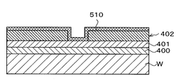
- a hydrophilic film having hydrophilicity may be formed on the exposed surface of the neutral layer 401.
- the first block G1 of the coating and developing treatment apparatus 2 is provided with a hydrophilic film forming apparatus 500 that forms a hydrophilic film by applying a hydrophilic coating liquid on the wafer W.
- the number and arrangement of the hydrophilic film forming apparatuses 500 can be arbitrarily selected.
- spin coating for applying a predetermined coating liquid on the wafer W is performed as in the other liquid processing apparatuses of the first block G1.
- the hydrophilic coating solution is not particularly limited, but in this embodiment, for example, a solution in which a hydroxyl group is bonded to polymethyl methacrylate (PMMA-OH) is used.
- the wafer W on which the resist pattern 402 is formed in step S3 is transferred to the hydrophilic film forming apparatus 500.
- the coating liquid is applied onto the exposed surface of the neutral layer 401 of the wafer W and the resist pattern 402 to form a hydrophilic film 510.
- the wafer W is transferred to the heat treatment apparatus 40, heated, and the temperature is adjusted.
- step S5 an organic solvent is supplied onto the wafer W by the cleaning device 31, and the hydrophilic film 510 on the resist pattern 402 is removed together with the resist pattern 402 on the wafer W as shown in FIG. Further, the upper portion of the hydrophilic film 510 on the exposed surface of the neutral layer 401 is also removed. Thus, a thin hydrophilic film 510 having a film thickness of, for example, 5 nm is formed only on the exposed surface of the neutral layer 401. Although the hydrophilic film 510 can be visually recognized in the illustrated example, the thickness of the hydrophilic film 510 is actually smaller than the thickness of the neutral layer 401 and the surface of the neutral layer 401 is kept flat. ing.
- the thin hydrophilic film 510 can be formed on the exposed surface of the neutral layer 401, the exposed surface can be hydrophilized. Therefore, the same effect as that of the above embodiment can be enjoyed. That is, a predetermined fine pattern of the hydrophilic polymer 405 can be appropriately formed on the wafer W, and the processing target film can be appropriately etched using the pattern as a mask in step S9. Further, the throughput of wafer processing in the substrate processing system 1 can be improved.
- the exposed surface of the neutral layer 401 is hydrophilized as the surface treatment in the step S4.
- the exposed surface may be hydrophobized.
- the first block G1 of the coating and developing treatment apparatus 2 is provided with a hydrophobic film forming apparatus 550 that forms a hydrophobic film by applying a hydrophobic coating liquid onto the wafer W.
- the number and arrangement of the hydrophobic film forming apparatuses 550 can be arbitrarily selected.
- spin coating for applying a predetermined coating liquid onto the wafer W is performed as in the other liquid processing apparatuses of the first block G1.
- the hydrophobic coating liquid is not particularly limited, but in this embodiment, for example, a liquid in which a hydroxyl group is bonded to polystyrene (PS-OH) is used.
- the wafer W on which the resist pattern 402 is formed in step S3 is transferred to the hydrophobic film forming apparatus 550.
- a coating liquid is applied onto the exposed surface of the neutral layer 401 of the wafer W and the resist pattern 402 to form a hydrophobic film.
- the wafer W is transferred to the heat treatment apparatus 40, heated, and the temperature is adjusted.
- step S5 an organic solvent is supplied onto the wafer W, and the hydrophobic film on the resist pattern 402 is removed together with the resist pattern 402 on the wafer W as shown in FIG. Further, the upper part of the hydrophobic film on the exposed surface of the neutral layer 401 is also removed. Thus, a thin hydrophobic film 560 having a thickness of, for example, 5 nm is formed only on the exposed surface of the neutral layer 401.
- step S7 since the exposed surface of the neutral layer 401 is hydrophobized in step S7, the hydrophobic polymer 406 is disposed in the middle of the hydrophobic film 560 on the hydrophobic film 560 as shown in FIG. Hydrophilic polymers 405 and 405 are disposed on both sides thereof. On the wafer W, the hydrophilic polymer 405 and the hydrophobic polymer 406 are alternately arranged in an arrangement opposite to the case where the exposed surface of the neutral layer 401 is made hydrophilic.
- the thin hydrophobic film 560 can be formed on the exposed surface of the neutral layer 401, the exposed surface can be hydrophobized. Therefore, the same effect as that of the above embodiment can be enjoyed. That is, a predetermined fine pattern of the hydrophilic polymer 405 can be appropriately formed on the wafer W, and the processing target film can be appropriately etched using the pattern as a mask in step S9. Further, the throughput of wafer processing in the substrate processing system 1 can be improved.
- the block copolymer 404 when the block copolymer 404 is applied on the flat neutral layer 401 in which the exposed surface exposed from the resist pattern 402 is hydrophilized or hydrophobized by surface treatment as described above. It was confirmed that the lamellar structure may not be phase-separated in a desired pattern. Specifically, the desired lamellar structure is, for example, along the longitudinal direction of the hydrophilic region 403 formed by surface-treating the neutral layer 401 as shown in FIG.
- the lamellar structure is arranged perpendicular to the longitudinal direction of the hydrophilic region 403, for example, as shown in FIG. May end up.
- drawing is abbreviate
- the hydrophilic region 403 has a width orthogonal to the longitudinal direction of the hydrophilic region 403 because the hydrophilic polymer 405 and the hydrophobic polymer 406 are alternately arranged in odd layers, for example, three layers.
- the reason is that the polymers 405 and 406 can be stretched. Therefore, the present inventors set the width of the space portion 402b of the resist pattern 402 to either one of the hydrophilic polymer 405 or the hydrophobic polymer 406 so that the lamella structure is not arranged perpendicular to the longitudinal direction of the hydrophilic region 403.
- the idea was to have one layer and less than two layers.
- the width of the space portion 402b is sufficiently fine for patterning with a resist even when the hydrophilic polymer 405 and the hydrophobic polymer 406 are alternately arranged in three layers. Cannot be formed of a resist.
- the present inventors considered that the width of the space portion 402b can be increased by heating the resist pattern 402 and increasing the width of the line portion 402a of the resist pattern 402 by so-called reflow. A specific method will be described below.
- the wafer W on which the resist pattern 402 is formed after the development and post-baking in step S3 is transferred to the heat treatment apparatus 40.
- the heat treatment apparatus 40 heating is performed at a temperature not lower than the glass transition point temperature of the resist and not higher than the heat resistant temperature of the resist for a predetermined time, for example, 160 ° C. for one minute.
- the heat treatment apparatus 40 functions as a reflow apparatus.
- the wafer W is heated by the heat treatment apparatus 40 at a temperature equal to or higher than the glass transition temperature, and reflow occurs. For example, as shown by a broken line in FIG. As shown by a solid line in FIG.
- the lower portion is deformed into a substantially inverted U shape with its sides extending laterally.
- the spread of the line portion 402a is controlled, and the space portion 402b has a desired width, that is, either a hydrophilic polymer 405 after phase separation into a lamellar structure or a hydrophobic polymer 406
- the width is adjusted to one or more layers and less than two layers.
- the line part 402a has a substantially uniform width across the longitudinal direction.
- FIG. 22A is a planar image of the resist pattern 402 when the wafer W is heated at 140 ° C. below the glass transition temperature of the resist
- FIG. 22B shows the temperature above the glass transition temperature of the resist. It is the image after heating the wafer W at 160 degreeC below the heat-resistant temperature of a resist, and making it reflow.
- reflow does not occur because the heating temperature is equal to or lower than the glass transition temperature of the resist.
- the width of the line portion 402a in plan view is widened by reflow, and the width of the space portion 402b. Can be confirmed.
- the wafer W in which the width of the space portion 402b is adjusted by reflow is transferred to the ultraviolet irradiation device 41 in step S4, and is exposed to the neutral layer 401 of the exposed space portion 402b exposed from the resist pattern 402 as shown in FIG. Ultraviolet rays are irradiated. As a result, a hydrophilic region 403 corresponding to one layer of the polymers 405 and 406 after phase separation is formed in the neutral layer 401.
- step S7 the block copolymer 404 is phase-separated into a hydrophilic polymer 405 and a hydrophobic polymer 406.
- the hydrophilic region 403 has a width corresponding to one layer of the hydrophilic polymer 405. Therefore, the hydrophilic polymer 405 is surely disposed in the hydrophilic region 403, and both sides thereof are arranged.
- Hydrophobic polymers 406 and 406 are disposed on the surface. And the hydrophilic polymer 405 and the hydrophobic polymer 406 are alternately arrange
- the width of the space portion 402b is, for example, one or more of the hydrophilic polymer 405 and the hydrophobic polymer 406 and less than two layers. It was adjusted. Therefore, when the block copolymer 404 is applied on the flat neutral layer 401 and phase-separated into a lamellar structure, the lamellar structure can be prevented from being arranged perpendicular to the longitudinal direction of the hydrophilic region 403. Therefore, in the present embodiment, the lamella structure can be reliably arranged along the longitudinal direction of the hydrophilic region 403.
- reflow is performed by heating with the heat treatment apparatus 40.
- a heat treatment apparatus dedicated to reflow may be separately provided in the coating and developing treatment apparatus 2.
- the reflow is performed by separately heating with the heat treatment apparatus 40.
- the reflow may be performed simultaneously by adjusting the heating time and the heating temperature in the post-baking.
- reflow may be performed by exposing the wafer W to a solvent atmosphere of the resist to dissolve the resist.
- the heating temperature and heating time for reflow are not limited to the above embodiment, and are appropriately set depending on the type of resist and its base film.
- the neutral layer 401 is hydrophilized by ultraviolet irradiation
- the hydrophilic film 510 is formed on the exposed surface of the neutral layer 401
- the width of the space portion 402b may be narrowed by reflow.
- the hydrophilic film 510 is formed as an example, as shown in FIG. 25, for example, the neutral layer 401 and the resist pattern 402 exposed in the space 402b narrowed to the width of one layer by reflow.
- a coating solution is applied on top of it to form a hydrophilic film 510.
- the hydrophilic film 510 is removed together with the resist pattern 402, and the hydrophilic film 510 is formed only in the space portion 402b whose width is narrowed by reflow.
- the hydrophilic film 510 having a width corresponding to one layer of the polymers 405 and 406 can be formed on the exposed surface of the neutral layer 401. Therefore, the same effect as when the hydrophilic region 403 is formed by ultraviolet irradiation can be obtained. That is, it is possible to prevent the lamellar structure from being arranged perpendicular to the longitudinal direction of the hydrophilic film 510.
- the block copolymer 404 on the wafer W is phase-separated into a hydrophilic polymer 405 having a lamellar structure and a hydrophobic polymer 406.
- the block copolymer 404 is made into a cylinder.
- the present invention can also be applied to the case of phase separation into a hydrophilic polymer 405 and a hydrophobic polymer 406 having a structure.
- the ratio of the molecular weight of the hydrophilic polymer 405 is 20% to 40%, and the ratio of the molecular weight of the hydrophobic polymer 406 in the block copolymer 404 is 80% to 60%. %.
- the substrate processing system 1 having the same structure as that of the above embodiment is used.
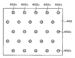
- step S3 a resist pattern having a circular space portion 402c in plan view is formed on the wafer W as shown in FIG.
- the space portions 402c are arranged in a staggered manner in a plan view.
- step S7 when the block copolymer 404 is phase-separated in step S7, it is phase-separated into a hydrophilic polymer 405 having a cylindrical structure and a hydrophobic polymer 406 as shown in FIG.
- the hydrophilic polymer 405 is formed on the hydrophilic space portion 402c and on the resist pattern 402 between the two space portions 402c and 402c.
- the hydrophobic polymer 406 is formed on the other resist pattern 402.
- step S9 when the hydrophilic polymer 405 is used as a mask to etch the film to be processed on the wafer W, a predetermined hole-shaped pattern is formed on the film to be processed.
- the block copolymer 404 can be appropriately phase-separated into the hydrophilic polymer 405 and the hydrophobic polymer 406 having a cylindrical structure, and the etching process of the film to be processed can be appropriately performed.
- the block copolymer 404 of the above embodiment has polymethyl methacrylate (PMMA) and polystyrene (PS), but includes a hydrophilic polymer having hydrophilicity and a hydrophobic polymer having hydrophobicity. It is not limited to this.
- silicone rubber (PDMS) may be used for the hydrophilic polymer.
- the neutralization or hydrophobization of the neutral layer 401 in step S4 has been performed by the coating and developing treatment apparatus 2 of the substrate processing system 1.
- the neutralization or hydrophobization of the neutral layer 401 is performed.
- the etching may be performed by etching apparatuses 202 to 205 of the etching processing apparatus 3, for example, an RIE apparatus.
- the film to be processed on the wafer W is etched in step S9, but the wafer processing method of the present invention can also be applied when etching the wafer W itself.
- the present invention is not limited to such examples. It is obvious for those skilled in the art that various modifications or modifications can be conceived within the scope of the idea described in the claims, and these naturally belong to the technical scope of the present invention. It is understood.
- the present invention is not limited to this example and can take various forms.
- the present invention can also be applied to a case where the substrate is another substrate such as an FPD (flat panel display) other than a wafer or a mask reticle for a photomask.
- FPD flat panel display
- the present invention is useful when a substrate is treated with a block copolymer containing, for example, a hydrophilic polymer having hydrophilicity and a hydrophobic polymer having hydrophobicity.
Landscapes
- Engineering & Computer Science (AREA)
- Manufacturing & Machinery (AREA)
- Microelectronics & Electronic Packaging (AREA)
- General Physics & Mathematics (AREA)
- Physics & Mathematics (AREA)
- Power Engineering (AREA)
- Condensed Matter Physics & Semiconductors (AREA)
- Computer Hardware Design (AREA)
- Chemical & Material Sciences (AREA)
- Inorganic Chemistry (AREA)
- Nanotechnology (AREA)
- Analytical Chemistry (AREA)
- Exposure Of Semiconductors, Excluding Electron Or Ion Beam Exposure (AREA)
- Formation Of Insulating Films (AREA)
- Exposure And Positioning Against Photoresist Photosensitive Materials (AREA)
- Photosensitive Polymer And Photoresist Processing (AREA)
Applications Claiming Priority (2)
| Application Number | Priority Date | Filing Date | Title |
|---|---|---|---|
| JP2012-196737 | 2012-09-07 | ||
| JP2012196737A JP5881565B2 (ja) | 2012-09-07 | 2012-09-07 | 基板処理方法、プログラム及びコンピュータ記憶媒体 |
Publications (1)
| Publication Number | Publication Date |
|---|---|
| WO2014038420A1 true WO2014038420A1 (ja) | 2014-03-13 |
Family
ID=50237032
Family Applications (1)
| Application Number | Title | Priority Date | Filing Date |
|---|---|---|---|
| PCT/JP2013/072704 Ceased WO2014038420A1 (ja) | 2012-09-07 | 2013-08-26 | 基板処理方法、コンピュータ記憶媒体及び基板処理システム |
Country Status (3)
| Country | Link |
|---|---|
| JP (1) | JP5881565B2 (enExample) |
| TW (1) | TW201426845A (enExample) |
| WO (1) | WO2014038420A1 (enExample) |
Cited By (1)
| Publication number | Priority date | Publication date | Assignee | Title |
|---|---|---|---|---|
| JP2016163010A (ja) * | 2015-03-05 | 2016-09-05 | 東京エレクトロン株式会社 | 基板処理方法、プログラム、コンピュータ記憶媒体及び基板処理システム |
Families Citing this family (3)
| Publication number | Priority date | Publication date | Assignee | Title |
|---|---|---|---|---|
| JP6177723B2 (ja) * | 2014-04-25 | 2017-08-09 | 東京エレクトロン株式会社 | 基板処理方法、プログラム、コンピュータ記憶媒体及び基板処理システム |
| JP6346115B2 (ja) * | 2015-03-24 | 2018-06-20 | 東芝メモリ株式会社 | パターン形成方法 |
| JP6494446B2 (ja) * | 2015-06-23 | 2019-04-03 | 東京エレクトロン株式会社 | 基板処理方法、プログラム及びコンピュータ記憶媒体 |
Citations (6)
| Publication number | Priority date | Publication date | Assignee | Title |
|---|---|---|---|---|
| JPH04364021A (ja) * | 1991-06-11 | 1992-12-16 | Sumitomo Electric Ind Ltd | 半導体装置の製造方法 |
| WO2007032467A1 (ja) * | 2005-09-16 | 2007-03-22 | National Agriculture And Food Research Organization | 樹脂製マイクロチャネルアレイの製造方法及びこれを用いた血液測定方法 |
| US7521090B1 (en) * | 2008-01-12 | 2009-04-21 | International Business Machines Corporation | Method of use of epoxy-containing cycloaliphatic acrylic polymers as orientation control layers for block copolymer thin films |
| US7521094B1 (en) * | 2008-01-14 | 2009-04-21 | International Business Machines Corporation | Method of forming polymer features by directed self-assembly of block copolymers |
| WO2011128120A1 (en) * | 2010-04-14 | 2011-10-20 | Asml Netherlands B.V. | Method for providing an ordered layer of self-assemblable polymer for use in lithography |
| WO2011151109A1 (en) * | 2010-06-04 | 2011-12-08 | Asml Netherlands B.V. | Self-assemblable polymer and method for use in lithography |
-
2012
- 2012-09-07 JP JP2012196737A patent/JP5881565B2/ja active Active
-
2013
- 2013-08-26 WO PCT/JP2013/072704 patent/WO2014038420A1/ja not_active Ceased
- 2013-09-02 TW TW102131552A patent/TW201426845A/zh unknown
Patent Citations (6)
| Publication number | Priority date | Publication date | Assignee | Title |
|---|---|---|---|---|
| JPH04364021A (ja) * | 1991-06-11 | 1992-12-16 | Sumitomo Electric Ind Ltd | 半導体装置の製造方法 |
| WO2007032467A1 (ja) * | 2005-09-16 | 2007-03-22 | National Agriculture And Food Research Organization | 樹脂製マイクロチャネルアレイの製造方法及びこれを用いた血液測定方法 |
| US7521090B1 (en) * | 2008-01-12 | 2009-04-21 | International Business Machines Corporation | Method of use of epoxy-containing cycloaliphatic acrylic polymers as orientation control layers for block copolymer thin films |
| US7521094B1 (en) * | 2008-01-14 | 2009-04-21 | International Business Machines Corporation | Method of forming polymer features by directed self-assembly of block copolymers |
| WO2011128120A1 (en) * | 2010-04-14 | 2011-10-20 | Asml Netherlands B.V. | Method for providing an ordered layer of self-assemblable polymer for use in lithography |
| WO2011151109A1 (en) * | 2010-06-04 | 2011-12-08 | Asml Netherlands B.V. | Self-assemblable polymer and method for use in lithography |
Non-Patent Citations (3)
| Title |
|---|
| BIN YU ET AL.: "Confinment-Induced Novel Morphologies of Block Copolymers, art 138306", PHYSICAL REVIEW LETTERS, vol. 96, 7 April 2006 (2006-04-07), pages 138306-1 - 138306-4 * |
| GREGORY S. DOERK ET AL.: "Pattern Placement Accuracy in Block Copolymer Directed Self- Assembly Based on Chemical Epitaxy", ACS NANO, vol. 7, no. 1, 30 November 2012 (2012-11-30), pages 276 - 285 * |
| JY CHENG ET AL.: "7.12 Block Copolymer Thin Films on Patterned Substrates", POLYMER SCIENCE: A COMPREHENSIVE REFERANCE, May 2012 (2012-05-01), pages 233 - 249 * |
Cited By (5)
| Publication number | Priority date | Publication date | Assignee | Title |
|---|---|---|---|---|
| JP2016163010A (ja) * | 2015-03-05 | 2016-09-05 | 東京エレクトロン株式会社 | 基板処理方法、プログラム、コンピュータ記憶媒体及び基板処理システム |
| WO2016140031A1 (ja) * | 2015-03-05 | 2016-09-09 | 東京エレクトロン株式会社 | 基板処理方法、コンピュータ記憶媒体及び基板処理システム |
| KR20170122199A (ko) * | 2015-03-05 | 2017-11-03 | 도쿄엘렉트론가부시키가이샤 | 기판 처리 방법, 컴퓨터 기억 매체 및 기판 처리 시스템 |
| US10329144B2 (en) | 2015-03-05 | 2019-06-25 | Tokyo Electron Limited | Substrate treatment method, computer storage medium and substrate treatment system |
| KR102510734B1 (ko) | 2015-03-05 | 2023-03-15 | 도쿄엘렉트론가부시키가이샤 | 기판 처리 방법, 컴퓨터 기억 매체 및 기판 처리 시스템 |
Also Published As
| Publication number | Publication date |
|---|---|
| TW201426845A (zh) | 2014-07-01 |
| JP5881565B2 (ja) | 2016-03-09 |
| JP2014053439A (ja) | 2014-03-20 |
Similar Documents
| Publication | Publication Date | Title |
|---|---|---|
| JP5919210B2 (ja) | 基板処理方法、プログラム、コンピュータ記憶媒体及び基板処理システム | |
| JP6141144B2 (ja) | 基板処理方法、プログラム、コンピュータ記憶媒体及び基板処理システム | |
| JP5881565B2 (ja) | 基板処理方法、プログラム及びコンピュータ記憶媒体 | |
| JP6081728B2 (ja) | 基板処理方法、コンピュータ記憶媒体及び基板処理システム | |
| JP2014187103A (ja) | 基板処理装置、基板処理方法、プログラム及びコンピュータ記憶媒体 | |
| JP2014027228A (ja) | 基板処理方法、プログラム、コンピュータ記憶媒体及び基板処理システム | |
| JP5823424B2 (ja) | 基板処理方法、プログラム、コンピュータ記憶媒体及び基板処理システム | |
| US9741583B2 (en) | Substrate treatment method, computer readable storage medium and substrate treatment system | |
| JP5837525B2 (ja) | 基板処理方法、プログラム及びコンピュータ記憶媒体 | |
| JP6045482B2 (ja) | 表面処理装置、表面処理方法、プログラム及びコンピュータ記憶媒体 | |
| JP6267143B2 (ja) | 基板処理方法、プログラム、コンピュータ記憶媒体及び基板処理システム | |
| KR102657313B1 (ko) | 기판 처리 방법 및 컴퓨터 기억 매체 | |
| JP5847738B2 (ja) | 基板処理方法、プログラム及びコンピュータ記憶媒体 | |
| WO2014046241A1 (ja) | 基板処理システム | |
| WO2017069200A1 (ja) | 基板処理方法及びコンピュータ記憶媒体 |
Legal Events
| Date | Code | Title | Description |
|---|---|---|---|
| 121 | Ep: the epo has been informed by wipo that ep was designated in this application |
Ref document number: 13835204 Country of ref document: EP Kind code of ref document: A1 |
|
| NENP | Non-entry into the national phase |
Ref country code: DE |
|
| 122 | Ep: pct application non-entry in european phase |
Ref document number: 13835204 Country of ref document: EP Kind code of ref document: A1 |