WO2014038420A1 - Substrate processing method, computer storage medium, and substrate processing system - Google Patents
Substrate processing method, computer storage medium, and substrate processing system Download PDFInfo
- Publication number
- WO2014038420A1 WO2014038420A1 PCT/JP2013/072704 JP2013072704W WO2014038420A1 WO 2014038420 A1 WO2014038420 A1 WO 2014038420A1 JP 2013072704 W JP2013072704 W JP 2013072704W WO 2014038420 A1 WO2014038420 A1 WO 2014038420A1
- Authority
- WO
- WIPO (PCT)
- Prior art keywords
- polymer
- neutral layer
- resist pattern
- block copolymer
- substrate processing
- Prior art date
Links
Images


Classifications
-
- H—ELECTRICITY
- H01—ELECTRIC ELEMENTS
- H01L—SEMICONDUCTOR DEVICES NOT COVERED BY CLASS H10
- H01L21/00—Processes or apparatus adapted for the manufacture or treatment of semiconductor or solid state devices or of parts thereof
- H01L21/02—Manufacture or treatment of semiconductor devices or of parts thereof
- H01L21/027—Making masks on semiconductor bodies for further photolithographic processing not provided for in group H01L21/18 or H01L21/34
- H01L21/033—Making masks on semiconductor bodies for further photolithographic processing not provided for in group H01L21/18 or H01L21/34 comprising inorganic layers
- H01L21/0334—Making masks on semiconductor bodies for further photolithographic processing not provided for in group H01L21/18 or H01L21/34 comprising inorganic layers characterised by their size, orientation, disposition, behaviour, shape, in horizontal or vertical plane
- H01L21/0337—Making masks on semiconductor bodies for further photolithographic processing not provided for in group H01L21/18 or H01L21/34 comprising inorganic layers characterised by their size, orientation, disposition, behaviour, shape, in horizontal or vertical plane characterised by the process involved to create the mask, e.g. lift-off masks, sidewalls, or to modify the mask, e.g. pre-treatment, post-treatment
-
- B—PERFORMING OPERATIONS; TRANSPORTING
- B81—MICROSTRUCTURAL TECHNOLOGY
- B81C—PROCESSES OR APPARATUS SPECIALLY ADAPTED FOR THE MANUFACTURE OR TREATMENT OF MICROSTRUCTURAL DEVICES OR SYSTEMS
- B81C1/00—Manufacture or treatment of devices or systems in or on a substrate
- B81C1/00015—Manufacture or treatment of devices or systems in or on a substrate for manufacturing microsystems
- B81C1/00023—Manufacture or treatment of devices or systems in or on a substrate for manufacturing microsystems without movable or flexible elements
- B81C1/00031—Regular or irregular arrays of nanoscale structures, e.g. etch mask layer
-
- G—PHYSICS
- G03—PHOTOGRAPHY; CINEMATOGRAPHY; ANALOGOUS TECHNIQUES USING WAVES OTHER THAN OPTICAL WAVES; ELECTROGRAPHY; HOLOGRAPHY
- G03F—PHOTOMECHANICAL PRODUCTION OF TEXTURED OR PATTERNED SURFACES, e.g. FOR PRINTING, FOR PROCESSING OF SEMICONDUCTOR DEVICES; MATERIALS THEREFOR; ORIGINALS THEREFOR; APPARATUS SPECIALLY ADAPTED THEREFOR
- G03F7/00—Photomechanical, e.g. photolithographic, production of textured or patterned surfaces, e.g. printing surfaces; Materials therefor, e.g. comprising photoresists; Apparatus specially adapted therefor
- G03F7/0002—Lithographic processes using patterning methods other than those involving the exposure to radiation, e.g. by stamping
-
- H—ELECTRICITY
- H01—ELECTRIC ELEMENTS
- H01L—SEMICONDUCTOR DEVICES NOT COVERED BY CLASS H10
- H01L21/00—Processes or apparatus adapted for the manufacture or treatment of semiconductor or solid state devices or of parts thereof
- H01L21/02—Manufacture or treatment of semiconductor devices or of parts thereof
- H01L21/027—Making masks on semiconductor bodies for further photolithographic processing not provided for in group H01L21/18 or H01L21/34
- H01L21/0271—Making masks on semiconductor bodies for further photolithographic processing not provided for in group H01L21/18 or H01L21/34 comprising organic layers
-
- H—ELECTRICITY
- H01—ELECTRIC ELEMENTS
- H01L—SEMICONDUCTOR DEVICES NOT COVERED BY CLASS H10
- H01L21/00—Processes or apparatus adapted for the manufacture or treatment of semiconductor or solid state devices or of parts thereof
- H01L21/67—Apparatus specially adapted for handling semiconductor or electric solid state devices during manufacture or treatment thereof; Apparatus specially adapted for handling wafers during manufacture or treatment of semiconductor or electric solid state devices or components ; Apparatus not specifically provided for elsewhere
- H01L21/67005—Apparatus not specifically provided for elsewhere
- H01L21/67011—Apparatus for manufacture or treatment
- H01L21/67155—Apparatus for manufacturing or treating in a plurality of work-stations
- H01L21/67161—Apparatus for manufacturing or treating in a plurality of work-stations characterized by the layout of the process chambers
- H01L21/67178—Apparatus for manufacturing or treating in a plurality of work-stations characterized by the layout of the process chambers vertical arrangement
-
- B—PERFORMING OPERATIONS; TRANSPORTING
- B81—MICROSTRUCTURAL TECHNOLOGY
- B81C—PROCESSES OR APPARATUS SPECIALLY ADAPTED FOR THE MANUFACTURE OR TREATMENT OF MICROSTRUCTURAL DEVICES OR SYSTEMS
- B81C2201/00—Manufacture or treatment of microstructural devices or systems
- B81C2201/01—Manufacture or treatment of microstructural devices or systems in or on a substrate
- B81C2201/0101—Shaping material; Structuring the bulk substrate or layers on the substrate; Film patterning
- B81C2201/0147—Film patterning
- B81C2201/0149—Forming nanoscale microstructures using auto-arranging or self-assembling material
-
- B—PERFORMING OPERATIONS; TRANSPORTING
- B82—NANOTECHNOLOGY
- B82Y—SPECIFIC USES OR APPLICATIONS OF NANOSTRUCTURES; MEASUREMENT OR ANALYSIS OF NANOSTRUCTURES; MANUFACTURE OR TREATMENT OF NANOSTRUCTURES
- B82Y40/00—Manufacture or treatment of nanostructures
Definitions
- the present invention relates to a substrate processing method, a computer storage medium, and a substrate processing system using a block copolymer including a hydrophilic polymer having hydrophilicity and a hydrophobic polymer having hydrophobicity.
- a resist coating process for coating a resist solution on a semiconductor wafer to form a resist film
- an exposure process for exposing a predetermined pattern on the resist film A photolithography process for sequentially performing a development process for developing the exposed resist film is performed to form a predetermined resist pattern on the wafer.
- an etching process is performed on the film to be processed on the wafer, and then a resist film removing process is performed to form a predetermined pattern on the film to be processed.
- Non-Patent Document 1 a wafer processing method using a block copolymer containing a hydrophilic polymer having hydrophilicity and a hydrophobic polymer having hydrophobicity has been proposed (Non-Patent Document 1).
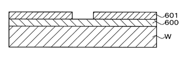
- a resist pattern is first formed on the antireflection film of the wafer, and then a neutral layer having an intermediate affinity for the hydrophilic polymer and the hydrophobic polymer is formed on the antireflection film and the resist pattern. To do. Thereafter, the neutral layer on the resist pattern is removed together with the resist pattern, and a pattern of the neutral layer 601 is formed on the antireflection film 600 of the wafer W as shown in FIG. Thereafter, as shown in FIG.
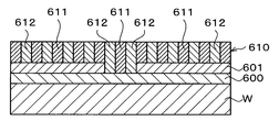
- a block copolymer 610 is applied on the antireflection film 600 and the neutral layer 601, and the hydrophilic polymer 611 and the hydrophobic polymer 612 are phase-separated from the block copolymer 610.
- the antireflection film 600 since the antireflection film 600 has hydrophilicity, on the antireflection film 600, for example, a hydrophobic polymer 612, a hydrophilic polymer 611, and a hydrophobic polymer 612 are separated in this order. Thereafter, for example, the hydrophilic polymer 611 is removed, whereby a fine pattern of the hydrophobic polymer 612 is formed on the wafer W. Then, the film to be processed is etched using the pattern of the hydrophobic polymer 612 as a mask, and a predetermined pattern is formed on the film to be processed.
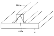
- Non-Patent Document 1 when the wafer processing method described in Non-Patent Document 1 is used, a portion where the antireflection film 600 is exposed in the neutral layer 601 is recessed on the wafer W as shown in FIG.
- the block copolymer 610 applied on the wafer W as shown in FIG. 29 the height of the pattern of the hydrophilic polymer 611 becomes non-uniform in the wafer surface.
- the etching depth in the wafer surface becomes non-uniform when etching the film to be processed using the pattern of the hydrophobic polymer 612 as a mask. For this reason, the etching process of a to-be-processed film cannot be performed appropriately, and a predetermined pattern may not be appropriately formed in a to-be-processed film.
- the present invention has been made in view of such points, and an object of the present invention is to appropriately form a predetermined pattern on a substrate in substrate processing using a block copolymer containing a hydrophilic polymer and a hydrophobic polymer.
- the present invention provides a method for treating a substrate using a block copolymer comprising a first polymer and a second polymer, wherein the first polymer and the second polymer are processed.
- a neutral layer forming step for forming a neutral layer having an intermediate affinity for the polymer on the substrate, and the substrate on which the resist pattern is formed on the neutral layer, exposed from the resist pattern Applying the block copolymer onto the neutral layer on the neutral layer treatment step for surface-treating the exposed surface of the neutral layer and the substrate from which the resist pattern has been removed after the neutral layer treatment step
- the exposed surface of the neutral layer exposed from the resist pattern is surface-treated, and the surface of the neutral layer is kept flat. If it does so, even if a block copolymer is apply
- Another aspect of the present invention is a readable computer storage medium storing a program that operates on a computer of a control unit that controls the substrate processing system so that the substrate processing method is executed by the substrate processing system.
- the present invention provides a system for processing a substrate using a block copolymer including a first polymer and a second polymer, wherein the first polymer and the second polymer are combined with each other.
- a neutral layer forming apparatus for forming a neutral layer having an intermediate affinity on the substrate, and the neutral layer exposed from the resist pattern with respect to the substrate on which the resist pattern is formed on the neutral layer
- a neutral layer processing apparatus for surface-treating an exposed surface of a layer; and the block copolymer for the substrate from which the resist pattern is removed after the exposed surface is surface-treated by the neutral layer processing apparatus.
- a block copolymer coating device for coating on a neutral layer; a polymer separation device for phase-separating the block copolymer on the neutral layer into the first polymer and the second polymer;
- a predetermined pattern can be appropriately formed on a substrate in substrate processing using a block copolymer containing a hydrophilic polymer and a hydrophobic polymer.
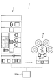
- FIG. 1 is an explanatory diagram showing an outline of a configuration of a substrate processing system 1 according to the present embodiment.
- the substrate processing system 1 includes a coating and developing apparatus 2 that performs photolithography processing on a wafer as a substrate, and an etching processing apparatus 3 that performs etching processing on the wafer.
- a film to be processed (not shown) is formed in advance on the wafer processed by the substrate processing system 1.
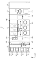
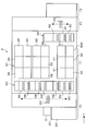
- the coating / developing apparatus 2 includes, for example, a cassette station 10 in which a cassette C containing a plurality of wafers W is carried in and out of the outside, and a predetermined type of sheet processing in a photolithography process.
- a processing station 11 having a plurality of various processing apparatuses for processing and an interface station 13 for transferring the wafer W between the exposure apparatus 12 adjacent to the processing station 11 are integrally connected. .
- the cassette station 10 is provided with a cassette mounting table 20.
- the cassette mounting table 20 is provided with a plurality of, for example, four cassette mounting plates 21.
- the cassette mounting plates 21 are arranged in a line in the horizontal X direction (vertical direction in FIG. 2).
- the cassette C can be placed on these cassette placement plates 21 when the cassette C is carried in and out of the coating and developing treatment apparatus 2.
- the cassette station 10 is provided with a wafer transfer device 23 that is movable on a transfer path 22 extending in the X direction.
- the wafer transfer device 23 is also movable in the vertical direction and the vertical axis direction ( ⁇ direction), and includes a cassette C on each cassette mounting plate 21 and a delivery device for a third block G3 of the processing station 11 described later.
- the wafer W can be transferred between the two.
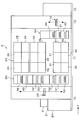
- the processing station 11 is provided with a plurality of, for example, four blocks G1, G2, G3, and G4 having various devices.
- the first block G1 is provided on the front side of the processing station 11 (X direction negative direction side in FIG. 2), and the second side is provided on the back side of the processing station 11 (X direction positive direction side in FIG. 2).
- Block G2 is provided.
- a third block G3 is provided on the cassette station 10 side (Y direction negative direction side in FIG. 1) of the processing station 11, and the interface station 13 side (Y direction positive direction side in FIG. 2) of the processing station 11 is provided. Is provided with a fourth block G4.
- a plurality of liquid processing apparatuses for example, a developing apparatus 30 for developing the wafer W, and a cleaning apparatus 31 for cleaning the wafer W by coating the wafer W with an organic solvent.
- An antireflection film forming device 32 for forming an antireflection film on the wafer W, a neutral layer forming device 33 for applying a neutral agent on the wafer W to form a neutral layer, and a resist solution on the wafer W Then, a resist coating device 34 for forming a resist film and a block copolymer coating device 35 for coating a block copolymer on the wafer W are stacked in order from the bottom.
- the developing device 30, the cleaning device 31, the antireflection film forming device 32, the neutral layer forming device 33, the resist coating device 34, and the block copolymer coating device 35 are arranged side by side in the horizontal direction.
- the number and arrangement of the developing device 30, the cleaning device 31, the antireflection film forming device 32, the neutral layer forming device 33, the resist coating device 34, and the block copolymer coating device 35 can be arbitrarily selected.
- the cleaning device 31, the antireflection film forming device 32, the neutral layer forming device 33, the resist coating device 34, and the block copolymer coating device 35 for example, a spin for applying a predetermined coating solution onto the wafer W. Coating is performed.
- spin coating for example, a coating liquid is discharged onto the wafer W from a coating nozzle, and the wafer W is rotated to diffuse the coating liquid to the surface of the wafer W.
- the block copolymer applied onto the wafer W by the block copolymer coating device 35 includes a first polymer and a second polymer.
- a hydrophobic polymer having hydrophobicity (nonpolar) is used as the first polymer
- a hydrophilic polymer having hydrophilicity (polarity) is used as the second polymer.
- PMMA polymethyl methacrylate
- PS polystyrene
- the ratio of the molecular weight of the hydrophilic polymer in the block copolymer is 40% to 60%, and the ratio of the molecular weight of the hydrophobic polymer in the block copolymer is 60% to 40%.
- the block copolymer is a polymer obtained by linearly combining these hydrophilic polymer and hydrophobic polymer.
- the neutral layer formed on the wafer W by the neutral layer forming apparatus 33 has an intermediate affinity for the hydrophilic polymer and the hydrophobic polymer.
- a random copolymer or an alternating copolymer of polymethyl methacrylate and polystyrene is used as the neutral layer.
- neutral means having an intermediate affinity for the hydrophilic polymer and the hydrophobic polymer.
- a heat treatment apparatus 40 that performs heat treatment of the wafer W, and a neutral layer treatment that performs surface treatment of the neutral layer by irradiating the neutral layer on the wafer W with ultraviolet rays.
- An ultraviolet irradiation device 41 as an apparatus, an adhesion device 42 for hydrophobizing the wafer W, and a peripheral exposure device 43 for exposing the outer periphery of the wafer W are provided side by side in the vertical and horizontal directions.
- the heat treatment apparatus 40 includes a hot plate for placing and heating the wafer W and a cooling plate for placing and cooling the wafer W, and can perform both heat treatment and cooling treatment.
- the ultraviolet irradiation device 41 includes a mounting table on which the wafer W is mounted, and an ultraviolet irradiation unit that irradiates the wafer W on the mounting table with ultraviolet light having a wavelength of 172 nm, for example.
- some of the heat treatment apparatuses 40 are polymers that cause the block copolymer coated on the wafer W by the block copolymer coating apparatus 35 to phase-separate into a hydrophilic polymer and a hydrophobic polymer. Functions as a separation device.
- the number and arrangement of the heat treatment apparatus 40, the ultraviolet irradiation apparatus 41, the adhesion apparatus 42, and the peripheral exposure apparatus 43 can be arbitrarily selected.
- a plurality of delivery devices 50, 51, 52, 53, 54, 55, 56 are provided in order from the bottom.
- the fourth block G4 is provided with a plurality of delivery devices 60, 61, 62 in order from the bottom.
- a wafer transfer area D is formed in an area surrounded by the first block G1 to the fourth block G4.
- a wafer transfer device 70 is disposed in the wafer transfer region D.
- the wafer transfer device 70 has, for example, a transfer arm that is movable in the Y direction, the X direction, the ⁇ direction, and the vertical direction.
- the wafer transfer device 70 moves in the wafer transfer area D and transfers the wafer W to a predetermined device in the surrounding first block G1, second block G2, third block G3, and fourth block G4. it can.
- a plurality of wafer transfer apparatuses 70 are arranged in the vertical direction, and can transfer the wafer W to a predetermined apparatus having the same height of each of the blocks G1 to G4, for example.
- a shuttle transfer device 80 that transfers the wafer W linearly between the third block G3 and the fourth block G4 is provided.
- the shuttle transport device 80 is linearly movable in the Y direction, for example.
- the shuttle transfer device 80 moves in the Y direction while supporting the wafer W, and can transfer the wafer W between the transfer device 52 of the third block G3 and the transfer device 62 of the fourth block G4.
- a wafer transfer device 100 is provided next to the third block G3 on the positive side in the X direction.
- the wafer transfer apparatus 100 has a transfer arm that is movable in the X direction, the ⁇ direction, and the vertical direction, for example.
- the wafer transfer device 100 can move up and down while supporting the wafer W, and can transfer the wafer W to each delivery device in the third block G3.
- the interface station 13 is provided with a wafer transfer device 110 and a delivery device 111.
- the wafer transfer device 110 has a transfer arm that is movable in the Y direction, the ⁇ direction, and the vertical direction, for example.
- the wafer transfer device 110 can transfer the wafer W between each transfer device, the transfer device 111, and the exposure device 12 in the fourth block G4, for example, by supporting the wafer W on a transfer arm.
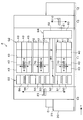
- the etching processing apparatus 3 includes a cassette station 200 that carries the wafer W into and out of the etching processing apparatus 3, a common transport unit 201 that transports the wafer W, and a block copolymer that is phase-separated on the wafer W.
- the cassette station 200 has a transfer chamber 211 in which a wafer transfer mechanism 210 for transferring the wafer W is provided.
- the wafer transfer mechanism 210 has two transfer arms 210a and 210b that hold the wafer W substantially horizontally, and is configured to transfer the wafer W while holding it by either of the transfer arms 210a and 210b.
- a cassette mounting table 212 on which a cassette C capable of accommodating a plurality of wafers W arranged side by side is mounted on the side of the transfer chamber 211. In the illustrated example, a plurality of, for example, three cassettes C can be mounted on the cassette mounting table 212.
- the transfer chamber 211 and the common transfer unit 201 are connected to each other via two load lock devices 213a and 213b that can be evacuated.
- the common transfer unit 201 includes a transfer chamber chamber 214 having a sealable structure formed to have a substantially polygonal shape (in the illustrated example, a hexagonal shape) as viewed from above, for example.
- a wafer transfer mechanism 215 for transferring the wafer W is provided in the transfer chamber 214.
- the wafer transfer mechanism 215 has two transfer arms 215a and 215b that hold the wafer W substantially horizontally, and is configured to transfer the wafer W while holding the wafer W by either of the transfer arms 215a and 215b. .
- Etching devices 202, 203, 204, 205 and load lock devices 213 b, 213 a are arranged outside the transfer chamber chamber 214 so as to surround the periphery of the transfer chamber chamber 214.
- the etching devices 202, 203, 204, 205 and the load lock devices 213b, 213a are arranged in this order in the clockwise direction when viewed from above, for example, and face the six side portions of the transfer chamber 214, respectively. Are arranged.
- an RIE (Reactive Ion Etching) apparatus is used as the etching apparatuses 202 to 205, for example. That is, in the etching apparatuses 202 to 205, dry etching for etching the hydrophobic polymer and the film to be processed is performed by reactive gas (etching gas), ions, and radicals.
- etching gas reactive gas
- ions ions
- radicals radicals
- the substrate processing system 1 described above is provided with a control unit 300 as shown in FIG.
- the control unit 300 is a computer, for example, and has a program storage unit (not shown).
- the program storage unit stores a program for controlling the processing of the wafer W in the substrate processing system 1.
- the program storage unit also stores a program for controlling the operation of driving systems such as the above-described various processing apparatuses and transfer apparatuses to realize a peeling process described later in the substrate processing system 1.
- the program is recorded on a computer-readable storage medium such as a computer-readable hard disk (HD), flexible disk (FD), compact disk (CD), magnetic optical desk (MO), or memory card. Or installed in the control unit 300 from the storage medium.
- HD computer-readable hard disk
- FD flexible disk
- CD compact disk
- MO magnetic optical desk
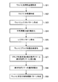
- FIG. 6 is a flowchart showing an example of main steps of such wafer processing.
- a cassette C containing a plurality of wafers W is carried into the cassette station 10 of the coating and developing treatment apparatus 2 and placed on a predetermined cassette placing plate 21. Thereafter, the wafers W in the cassette C are sequentially taken out by the wafer transfer device 23 and transferred to the transfer device 53 of the processing station 11.
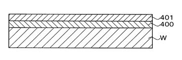
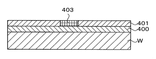
- the wafer W is transferred to the heat treatment apparatus 40 by the wafer transfer apparatus 70 and the temperature is adjusted. Thereafter, the wafer W is transferred to the antireflection film forming apparatus 32 by the wafer transfer apparatus 70, and an antireflection film 400 is formed on the wafer W as shown in FIG. 7 (step S1 in FIG. 6). Thereafter, the wafer W is transferred to the heat treatment apparatus 40, heated, and the temperature is adjusted.
- the wafer W is transferred to the neutral layer forming device 33 by the wafer transfer device 70.
- the neutral layer forming apparatus 33 as shown in FIG. 7, a neutral agent is applied on the antireflection film 400 of the wafer W to form a neutral layer 401 (step S2 in FIG. 6).
- the wafer W is transferred to the heat treatment apparatus 40, heated, temperature-controlled, and then returned to the delivery apparatus 53.
- the wafer W is transferred to the delivery device 54 by the wafer transfer device 100. Thereafter, the wafer W is transferred to the adhesion device 42 by the wafer transfer device 70 and subjected to an adhesion process. Thereafter, the wafer W is transferred to the resist coating device 34 by the wafer transfer device 70, and a resist solution is applied onto the neutral layer 401 of the wafer W to form a resist film. Thereafter, the wafer W is transferred to the heat treatment apparatus 40 by the wafer transfer apparatus 70 and pre-baked. Thereafter, the wafer W is transferred to the delivery device 55 by the wafer transfer device 70.
- the wafer W is transferred to the peripheral exposure device 43 by the wafer transfer device 70 and subjected to peripheral exposure processing. Thereafter, the wafer W is transferred to the delivery device 56 by the wafer transfer device 70.
- the wafer W is transferred to the transfer device 52 by the wafer transfer device 100 and transferred to the transfer device 62 by the shuttle transfer device 80.
- the wafer W is transferred to the exposure apparatus 12 by the wafer transfer apparatus 110 of the interface station 13 and subjected to exposure processing.
- the wafer W is transferred from the exposure apparatus 12 to the delivery apparatus 60 by the wafer transfer apparatus 110. Thereafter, the wafer W is transferred to the heat treatment apparatus 40 by the wafer transfer apparatus 70 and subjected to post-exposure baking. Thereafter, the wafer W is transferred to the developing device 30 by the wafer transfer device 70 and developed. After the development is completed, the wafer W is transferred to the heat treatment apparatus 40 by the wafer transfer apparatus 70 and subjected to a post-bake process.
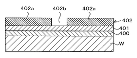
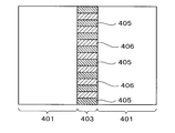
- a predetermined resist pattern 402 is formed on the neutral layer 401 of the wafer W as shown in FIG. 8 (step S3 in FIG. 6). In this embodiment, the resist pattern 402 has a linear shape in plan view.
- the width of the space portion 402b is set so that the hydrophilic polymer 405 and the hydrophobic polymer 406 are alternately arranged in the odd number layers in the space portion 402b as described later.
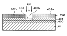
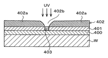
- the wafer W on which the resist pattern 402 is formed is transferred to the ultraviolet irradiation device 41 by the wafer transfer device 70.
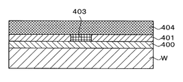
- the ultraviolet irradiation device 41 as shown in FIG. 9, the exposed surface of the neutral layer 401 exposed from the resist pattern 402 (space portion 402b) is irradiated with ultraviolet rays. At this time, ultraviolet rays having a wavelength of 172 nm are irradiated. Then, the exposed surface of the neutral layer 401 is oxidized and hydrophilized (step S4 in FIG. 6).
- the region of the neutral layer 401 thus made hydrophilic may be referred to as a hydrophilic region 403.
- the wavelength of ultraviolet rays for forming the hydrophilic region 403 in the neutral layer 401 may be 300 nm or less.
- active oxygen can be generated from oxygen in the processing atmosphere, and the exposed surface of the neutral layer 401 is oxidized and hydrophilized by this active oxygen.
- active oxygen in order to generate
- the wavelength of ultraviolet rays is 172 nm, not only when ozone is used as a processing atmosphere, but also when the processing atmosphere is an air atmosphere, active oxygen can be efficiently generated from oxygen in the air atmosphere. I know it.
- the wafer W is transferred to the cleaning device 31 by the wafer transfer device 70.
- the cleaning device 31 an organic solvent is supplied onto the wafer W, and the resist pattern 402 on the wafer W is removed as shown in FIG. 10 (step S5 in FIG. 6).
- the neutral layer 401 the surface of the hydrophilic region 403 has hydrophilicity, and the surface of other regions has neutrality. And the surface of the neutral layer 401 is maintained flat.
- the wafer W is transferred to the delivery device 50 by the wafer transfer device 70.
- the wafer W is transferred to the delivery device 55 by the wafer transfer device 100. Thereafter, the wafer W is transferred to the block copolymer coating device 35 by the wafer transfer device 70.
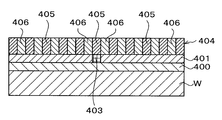
- the block copolymer coating device 35 the block copolymer 404 is coated on the neutral layer 401 of the wafer W as shown in FIG. 11 (step S6 in FIG. 6). At this time, since the surface of the neutral layer 401 is kept flat, the block copolymer 404 is also applied so as to have a uniform film thickness.
- the wafer W is transferred to the heat treatment apparatus 40 by the wafer transfer apparatus 70.
- a heat treatment at a predetermined temperature is performed on the wafer W.
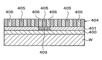
- the block copolymer 404 on the wafer W is phase-separated into the hydrophilic polymer 405 and the hydrophobic polymer 406 (step S7 in FIG. 6).
- the molecular weight ratio of the hydrophilic polymer 405 is 40% to 60%
- the molecular weight ratio of the hydrophobic polymer 406 is 60% to 40%.
- step S6 as shown in FIGS. 12 and 13
- the hydrophilic polymer 405 and the hydrophobic polymer 406 are phase-separated into a lamellar structure.
- the width of the space portion 402b of the resist pattern 402 is formed to a predetermined width in the above-described step S3
- the hydrophilic polymer 405 and the hydrophobic polymer 406 are formed on the hydrophilic region 403 of the neutral layer 401. Alternatingly arranged in odd layers, for example, three layers.
- the hydrophilic polymer 405 is disposed in the middle on the hydrophilic region 403, and the hydrophobic polymers 406 and 406 are disposed on both sides thereof. And the hydrophilic polymer 405 and the hydrophobic polymer 406 are alternately arrange
- the wafer W is transferred to the delivery device 50 by the wafer transfer device 70, and then transferred to the cassette C of the predetermined cassette mounting plate 21 by the wafer transfer device 23 of the cassette station 10.
- the cassette C containing the wafer W is unloaded from the coating and developing treatment apparatus 2 and then loaded into the etching processing apparatus 3.
- one wafer W is taken out from the cassette C on the cassette mounting table 212 by the wafer transfer mechanism 210 and loaded into the load lock apparatus 213 a.
- the inside of the load lock device 213a is sealed and decompressed.
- the inside of the load lock device 213a and the inside of the transfer chamber chamber 214 in a state where the pressure is reduced with respect to the atmospheric pressure (for example, a substantially vacuum state) are communicated.
- the wafer transfer mechanism 215 unloads the wafer W from the load lock device 213a and loads it into the transfer chamber 214.
- the wafer W carried into the transfer chamber 214 is then transferred to the etching apparatus 202 by the wafer transfer mechanism 215.
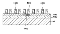
- the wafer W is etched, and the hydrophilic polymer 405 is selectively removed as shown in FIG. 14 to form a predetermined pattern of the hydrophobic polymer 406 (step S8 in FIG. 6).
- the pattern height of the hydrophobic polymer 406 is also uniform.
- the wafer W is transferred to the etching apparatus 204 by the wafer transfer mechanism 215.
- the film to be processed on the wafer W is etched using the hydrophobic polymer 406 on the wafer W as a mask.
- the hydrophobic polymer 406 and the antireflection film are removed, and a predetermined pattern is formed on the film to be processed (step S9 in FIG. 6).
- the wafer W is returned again into the transfer chamber 214 by the wafer transfer mechanism 215. Then, the wafer is transferred to the wafer transfer mechanism 210 via the load lock device 213b and stored in the cassette C. Thereafter, the cassette C containing the wafers W is unloaded from the etching processing apparatus 3 and a series of wafer processing ends.
- step S4 the exposed surface of the neutral layer 401 exposed from the resist pattern 402 (space portion 402b) is subjected to surface treatment to make it hydrophilic, and the surface of the neutral layer 401 is flattened. Maintained. Then, even if the block copolymer 404 is applied on the neutral layer 401 in the subsequent step S6, the surface of the block copolymer 404 is formed flat. For this reason, the pattern height of the hydrophobic polymer 406 formed on the wafer W by performing the subsequent steps S7 and S8 can be made uniform.
- a predetermined fine pattern of the hydrophobic polymer 406 can be appropriately formed on the wafer W, the etching process of the film to be processed using the pattern as a mask can be appropriately performed in step S9.
- a predetermined pattern can be formed on the film to be processed.
- the neutral layer is also etched using the resist pattern as a mask.
- the surface from which the neutral layer has been removed has hydrophilicity due to the exposure of the antireflection film, and the surface on which the neutral layer remains has neutrality.
- the wafer W has to be once taken out of the coating and developing treatment apparatus 2 and transferred to the etching treatment apparatus 3.
- step S4 of the present embodiment in the ultraviolet irradiation device 41 in the coating and developing treatment apparatus 2, the exposed surface of the neutral layer 401 is subjected to surface treatment by ultraviolet irradiation to make it hydrophilic. Accordingly, the transfer of the wafer W from the coating and developing treatment apparatus 2 to the etching treatment apparatus 3 can be omitted.
- the wafer processing in steps S1 to S7 is performed by one coating and developing processing apparatus 2. Therefore, the throughput of wafer processing in the substrate processing system 1 can be improved.
- the wavelength of ultraviolet light applied to the exposed surface of the neutral layer 401 in step S4 is 172 nm, active oxygen is efficiently generated from oxygen in the air atmosphere as compared with the case of using ultraviolet light with other wavelengths. be able to. Therefore, the exposed surface of the neutral layer 401 can be more easily made hydrophilic.
- the resist pattern 402 formed in step S3 is a line-and-space resist pattern.
- the molecular weight ratio of the hydrophilic polymer 405 in the block copolymer 404 is 40% to 60%.
- the molecular weight of the hydrophobic polymer 406 is Therefore, in step S7, the block copolymer 404 can be phase-separated into a hydrophilic polymer 405 and a hydrophobic polymer 406 in a lamellar structure.
- the width of the space portion 402b of the resist pattern 402 is formed to a predetermined width in the above-described step S3, the hydrophilic polymer 405 and the hydrophobic polymer 406 are formed on the hydrophilic region 403 of the neutral layer 401. Alternatingly arranged in odd layers, for example, three layers. Then, the hydrophilic polymer 405 and the hydrophobic polymer 406 can be formed on the wafer W with an appropriate lamellar structure.
- the exposed surface of the neutral layer 401 is irradiated with ultraviolet rays in step S4 to make the exposed surface hydrophilic, but the means for making the exposed surface hydrophilic is not limited to this.
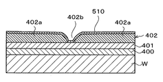
- a hydrophilic film having hydrophilicity may be formed on the exposed surface of the neutral layer 401.
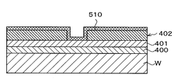
- the first block G1 of the coating and developing treatment apparatus 2 is provided with a hydrophilic film forming apparatus 500 that forms a hydrophilic film by applying a hydrophilic coating liquid on the wafer W.
- the number and arrangement of the hydrophilic film forming apparatuses 500 can be arbitrarily selected.
- spin coating for applying a predetermined coating liquid on the wafer W is performed as in the other liquid processing apparatuses of the first block G1.
- the hydrophilic coating solution is not particularly limited, but in this embodiment, for example, a solution in which a hydroxyl group is bonded to polymethyl methacrylate (PMMA-OH) is used.
- the wafer W on which the resist pattern 402 is formed in step S3 is transferred to the hydrophilic film forming apparatus 500.
- the coating liquid is applied onto the exposed surface of the neutral layer 401 of the wafer W and the resist pattern 402 to form a hydrophilic film 510.
- the wafer W is transferred to the heat treatment apparatus 40, heated, and the temperature is adjusted.
- step S5 an organic solvent is supplied onto the wafer W by the cleaning device 31, and the hydrophilic film 510 on the resist pattern 402 is removed together with the resist pattern 402 on the wafer W as shown in FIG. Further, the upper portion of the hydrophilic film 510 on the exposed surface of the neutral layer 401 is also removed. Thus, a thin hydrophilic film 510 having a film thickness of, for example, 5 nm is formed only on the exposed surface of the neutral layer 401. Although the hydrophilic film 510 can be visually recognized in the illustrated example, the thickness of the hydrophilic film 510 is actually smaller than the thickness of the neutral layer 401 and the surface of the neutral layer 401 is kept flat. ing.
- the thin hydrophilic film 510 can be formed on the exposed surface of the neutral layer 401, the exposed surface can be hydrophilized. Therefore, the same effect as that of the above embodiment can be enjoyed. That is, a predetermined fine pattern of the hydrophilic polymer 405 can be appropriately formed on the wafer W, and the processing target film can be appropriately etched using the pattern as a mask in step S9. Further, the throughput of wafer processing in the substrate processing system 1 can be improved.
- the exposed surface of the neutral layer 401 is hydrophilized as the surface treatment in the step S4.
- the exposed surface may be hydrophobized.
- the first block G1 of the coating and developing treatment apparatus 2 is provided with a hydrophobic film forming apparatus 550 that forms a hydrophobic film by applying a hydrophobic coating liquid onto the wafer W.
- the number and arrangement of the hydrophobic film forming apparatuses 550 can be arbitrarily selected.
- spin coating for applying a predetermined coating liquid onto the wafer W is performed as in the other liquid processing apparatuses of the first block G1.
- the hydrophobic coating liquid is not particularly limited, but in this embodiment, for example, a liquid in which a hydroxyl group is bonded to polystyrene (PS-OH) is used.
- the wafer W on which the resist pattern 402 is formed in step S3 is transferred to the hydrophobic film forming apparatus 550.
- a coating liquid is applied onto the exposed surface of the neutral layer 401 of the wafer W and the resist pattern 402 to form a hydrophobic film.
- the wafer W is transferred to the heat treatment apparatus 40, heated, and the temperature is adjusted.
- step S5 an organic solvent is supplied onto the wafer W, and the hydrophobic film on the resist pattern 402 is removed together with the resist pattern 402 on the wafer W as shown in FIG. Further, the upper part of the hydrophobic film on the exposed surface of the neutral layer 401 is also removed. Thus, a thin hydrophobic film 560 having a thickness of, for example, 5 nm is formed only on the exposed surface of the neutral layer 401.
- step S7 since the exposed surface of the neutral layer 401 is hydrophobized in step S7, the hydrophobic polymer 406 is disposed in the middle of the hydrophobic film 560 on the hydrophobic film 560 as shown in FIG. Hydrophilic polymers 405 and 405 are disposed on both sides thereof. On the wafer W, the hydrophilic polymer 405 and the hydrophobic polymer 406 are alternately arranged in an arrangement opposite to the case where the exposed surface of the neutral layer 401 is made hydrophilic.
- the thin hydrophobic film 560 can be formed on the exposed surface of the neutral layer 401, the exposed surface can be hydrophobized. Therefore, the same effect as that of the above embodiment can be enjoyed. That is, a predetermined fine pattern of the hydrophilic polymer 405 can be appropriately formed on the wafer W, and the processing target film can be appropriately etched using the pattern as a mask in step S9. Further, the throughput of wafer processing in the substrate processing system 1 can be improved.
- the block copolymer 404 when the block copolymer 404 is applied on the flat neutral layer 401 in which the exposed surface exposed from the resist pattern 402 is hydrophilized or hydrophobized by surface treatment as described above. It was confirmed that the lamellar structure may not be phase-separated in a desired pattern. Specifically, the desired lamellar structure is, for example, along the longitudinal direction of the hydrophilic region 403 formed by surface-treating the neutral layer 401 as shown in FIG.
- the lamellar structure is arranged perpendicular to the longitudinal direction of the hydrophilic region 403, for example, as shown in FIG. May end up.
- drawing is abbreviate
- the hydrophilic region 403 has a width orthogonal to the longitudinal direction of the hydrophilic region 403 because the hydrophilic polymer 405 and the hydrophobic polymer 406 are alternately arranged in odd layers, for example, three layers.
- the reason is that the polymers 405 and 406 can be stretched. Therefore, the present inventors set the width of the space portion 402b of the resist pattern 402 to either one of the hydrophilic polymer 405 or the hydrophobic polymer 406 so that the lamella structure is not arranged perpendicular to the longitudinal direction of the hydrophilic region 403.
- the idea was to have one layer and less than two layers.
- the width of the space portion 402b is sufficiently fine for patterning with a resist even when the hydrophilic polymer 405 and the hydrophobic polymer 406 are alternately arranged in three layers. Cannot be formed of a resist.
- the present inventors considered that the width of the space portion 402b can be increased by heating the resist pattern 402 and increasing the width of the line portion 402a of the resist pattern 402 by so-called reflow. A specific method will be described below.
- the wafer W on which the resist pattern 402 is formed after the development and post-baking in step S3 is transferred to the heat treatment apparatus 40.
- the heat treatment apparatus 40 heating is performed at a temperature not lower than the glass transition point temperature of the resist and not higher than the heat resistant temperature of the resist for a predetermined time, for example, 160 ° C. for one minute.
- the heat treatment apparatus 40 functions as a reflow apparatus.
- the wafer W is heated by the heat treatment apparatus 40 at a temperature equal to or higher than the glass transition temperature, and reflow occurs. For example, as shown by a broken line in FIG. As shown by a solid line in FIG.
- the lower portion is deformed into a substantially inverted U shape with its sides extending laterally.
- the spread of the line portion 402a is controlled, and the space portion 402b has a desired width, that is, either a hydrophilic polymer 405 after phase separation into a lamellar structure or a hydrophobic polymer 406
- the width is adjusted to one or more layers and less than two layers.
- the line part 402a has a substantially uniform width across the longitudinal direction.
- FIG. 22A is a planar image of the resist pattern 402 when the wafer W is heated at 140 ° C. below the glass transition temperature of the resist
- FIG. 22B shows the temperature above the glass transition temperature of the resist. It is the image after heating the wafer W at 160 degreeC below the heat-resistant temperature of a resist, and making it reflow.
- reflow does not occur because the heating temperature is equal to or lower than the glass transition temperature of the resist.
- the width of the line portion 402a in plan view is widened by reflow, and the width of the space portion 402b. Can be confirmed.
- the wafer W in which the width of the space portion 402b is adjusted by reflow is transferred to the ultraviolet irradiation device 41 in step S4, and is exposed to the neutral layer 401 of the exposed space portion 402b exposed from the resist pattern 402 as shown in FIG. Ultraviolet rays are irradiated. As a result, a hydrophilic region 403 corresponding to one layer of the polymers 405 and 406 after phase separation is formed in the neutral layer 401.
- step S7 the block copolymer 404 is phase-separated into a hydrophilic polymer 405 and a hydrophobic polymer 406.
- the hydrophilic region 403 has a width corresponding to one layer of the hydrophilic polymer 405. Therefore, the hydrophilic polymer 405 is surely disposed in the hydrophilic region 403, and both sides thereof are arranged.
- Hydrophobic polymers 406 and 406 are disposed on the surface. And the hydrophilic polymer 405 and the hydrophobic polymer 406 are alternately arrange
- the width of the space portion 402b is, for example, one or more of the hydrophilic polymer 405 and the hydrophobic polymer 406 and less than two layers. It was adjusted. Therefore, when the block copolymer 404 is applied on the flat neutral layer 401 and phase-separated into a lamellar structure, the lamellar structure can be prevented from being arranged perpendicular to the longitudinal direction of the hydrophilic region 403. Therefore, in the present embodiment, the lamella structure can be reliably arranged along the longitudinal direction of the hydrophilic region 403.
- reflow is performed by heating with the heat treatment apparatus 40.
- a heat treatment apparatus dedicated to reflow may be separately provided in the coating and developing treatment apparatus 2.
- the reflow is performed by separately heating with the heat treatment apparatus 40.
- the reflow may be performed simultaneously by adjusting the heating time and the heating temperature in the post-baking.
- reflow may be performed by exposing the wafer W to a solvent atmosphere of the resist to dissolve the resist.
- the heating temperature and heating time for reflow are not limited to the above embodiment, and are appropriately set depending on the type of resist and its base film.
- the neutral layer 401 is hydrophilized by ultraviolet irradiation
- the hydrophilic film 510 is formed on the exposed surface of the neutral layer 401
- the width of the space portion 402b may be narrowed by reflow.
- the hydrophilic film 510 is formed as an example, as shown in FIG. 25, for example, the neutral layer 401 and the resist pattern 402 exposed in the space 402b narrowed to the width of one layer by reflow.
- a coating solution is applied on top of it to form a hydrophilic film 510.
- the hydrophilic film 510 is removed together with the resist pattern 402, and the hydrophilic film 510 is formed only in the space portion 402b whose width is narrowed by reflow.
- the hydrophilic film 510 having a width corresponding to one layer of the polymers 405 and 406 can be formed on the exposed surface of the neutral layer 401. Therefore, the same effect as when the hydrophilic region 403 is formed by ultraviolet irradiation can be obtained. That is, it is possible to prevent the lamellar structure from being arranged perpendicular to the longitudinal direction of the hydrophilic film 510.
- the block copolymer 404 on the wafer W is phase-separated into a hydrophilic polymer 405 having a lamellar structure and a hydrophobic polymer 406.
- the block copolymer 404 is made into a cylinder.
- the present invention can also be applied to the case of phase separation into a hydrophilic polymer 405 and a hydrophobic polymer 406 having a structure.
- the ratio of the molecular weight of the hydrophilic polymer 405 is 20% to 40%, and the ratio of the molecular weight of the hydrophobic polymer 406 in the block copolymer 404 is 80% to 60%. %.
- the substrate processing system 1 having the same structure as that of the above embodiment is used.
- step S3 a resist pattern having a circular space portion 402c in plan view is formed on the wafer W as shown in FIG.
- the space portions 402c are arranged in a staggered manner in a plan view.
- step S7 when the block copolymer 404 is phase-separated in step S7, it is phase-separated into a hydrophilic polymer 405 having a cylindrical structure and a hydrophobic polymer 406 as shown in FIG.
- the hydrophilic polymer 405 is formed on the hydrophilic space portion 402c and on the resist pattern 402 between the two space portions 402c and 402c.
- the hydrophobic polymer 406 is formed on the other resist pattern 402.
- step S9 when the hydrophilic polymer 405 is used as a mask to etch the film to be processed on the wafer W, a predetermined hole-shaped pattern is formed on the film to be processed.
- the block copolymer 404 can be appropriately phase-separated into the hydrophilic polymer 405 and the hydrophobic polymer 406 having a cylindrical structure, and the etching process of the film to be processed can be appropriately performed.
- the block copolymer 404 of the above embodiment has polymethyl methacrylate (PMMA) and polystyrene (PS), but includes a hydrophilic polymer having hydrophilicity and a hydrophobic polymer having hydrophobicity. It is not limited to this.
- silicone rubber (PDMS) may be used for the hydrophilic polymer.
- the neutralization or hydrophobization of the neutral layer 401 in step S4 has been performed by the coating and developing treatment apparatus 2 of the substrate processing system 1.
- the neutralization or hydrophobization of the neutral layer 401 is performed.
- the etching may be performed by etching apparatuses 202 to 205 of the etching processing apparatus 3, for example, an RIE apparatus.
- the film to be processed on the wafer W is etched in step S9, but the wafer processing method of the present invention can also be applied when etching the wafer W itself.
- the present invention is not limited to such examples. It is obvious for those skilled in the art that various modifications or modifications can be conceived within the scope of the idea described in the claims, and these naturally belong to the technical scope of the present invention. It is understood.
- the present invention is not limited to this example and can take various forms.
- the present invention can also be applied to a case where the substrate is another substrate such as an FPD (flat panel display) other than a wafer or a mask reticle for a photomask.
- FPD flat panel display
- the present invention is useful when a substrate is treated with a block copolymer containing, for example, a hydrophilic polymer having hydrophilicity and a hydrophobic polymer having hydrophobicity.
Abstract
The present invention is a method which processes a substrate, using a block copolymer including a first polymer and a second polymer, wherein: a neutral layer having an intermediate affinity with respect to the first polymer and the second polymer is formed upon a substrate; with respect to the substrate whereupon a resist layer is formed upon the neutral layer, an exposed face of the neutral layer which is exposed from the resist layer is surface processed; thereafter, with respect to the substrate whereupon the resist pattern has been removed, a block copolymer is coated upon the neutral layer; and the block copolymer upon the neutral layer is phase separated into the first polymer and the second polymer.
Description
本願は、2012年9月7日に日本国に出願された特願2012-196737号に基づき、優先権を主張し、その内容をここに援用する。
本発明は、親水性を有する親水性ポリマーと疎水性を有する疎水性ポリマーとを含むブロック共重合体を用いた基板処理方法、コンピュータ記憶媒体及び基板処理システムに関する。 This application claims priority based on Japanese Patent Application No. 2012-196737 filed in Japan on September 7, 2012, the contents of which are incorporated herein by reference.
The present invention relates to a substrate processing method, a computer storage medium, and a substrate processing system using a block copolymer including a hydrophilic polymer having hydrophilicity and a hydrophobic polymer having hydrophobicity.
例えば半導体デバイスの製造工程では、例えば半導体ウェハ(以下、「ウェハ」という。)上にレジスト液を塗布してレジスト膜を形成するレジスト塗布処理、当該レジスト膜に所定のパターンを露光する露光処理、露光されたレジスト膜を現像する現像処理などを順次行うフォトリソグラフィー処理が行われ、ウェハ上に所定のレジストパターンが形成される。そして、このレジストパターンをマスクとして、ウェハ上の被処理膜のエッチング処理が行われ、その後レジスト膜の除去処理などが行われて、被処理膜に所定のパターンが形成される。
For example, in the manufacturing process of a semiconductor device, for example, a resist coating process for coating a resist solution on a semiconductor wafer (hereinafter referred to as “wafer”) to form a resist film, an exposure process for exposing a predetermined pattern on the resist film, A photolithography process for sequentially performing a development process for developing the exposed resist film is performed to form a predetermined resist pattern on the wafer. Then, using the resist pattern as a mask, an etching process is performed on the film to be processed on the wafer, and then a resist film removing process is performed to form a predetermined pattern on the film to be processed.
ところで、近年、半導体デバイスのさらなる高集積化を図るため、上述した被処理膜のパターンの微細化が求められている。このため、レジストパターンの微細化が進められており、例えばフォトリソグラフィー処理における露光処理の光を短波長化することが進められている。しかしながら、露光光源の短波長化には技術的、コスト的な限界があり、光の短波長化を進める方法のみでは、例えば数ナノメートルオーダーの微細なレジストパターンを形成するのが困難な状況にある。
Incidentally, in recent years, in order to further increase the integration of semiconductor devices, it is required to make the pattern of the film to be processed finer. For this reason, miniaturization of the resist pattern has been advanced, and for example, the light of the exposure process in the photolithography process has been shortened. However, there are technical and cost limitations to shortening the wavelength of the exposure light source, and it is difficult to form a fine resist pattern on the order of several nanometers, for example, only by the method of advancing the wavelength of light. is there.
そこで、親水性を有する親水性ポリマーと疎水性を有する疎水性ポリマーとを含むブロック共重合体を用いたウェハ処理方法が提案されている(非特許文献1)。かかる方法では、先ず、ウェハの反射防止膜上にレジストパターンを形成した後、反射防止膜とレジストパターン上に、親水性ポリマーと疎水性ポリマーに対して中間の親和性を有する中性層を形成する。その後、レジストパターンと共に、当該レジストパターン上の中性層を除去し、図28に示すようにウェハWの反射防止膜600上に中性層601のパターンを形成する。その後、図29に示すように反射防止膜600と中性層601上にブロック共重合体610を塗布し、ブロック共重合体610から親水性ポリマー611と疎水性ポリマー612を相分離する。このとき、反射防止膜600が親水性を有するので、反射防止膜600上には、例えば疎水性ポリマー612、親水性ポリマー611、疎水性ポリマー612がこの順で並べて分離される。その後、例えば親水性ポリマー611を除去することで、ウェハW上に疎水性ポリマー612の微細なパターンが形成される。そして、疎水性ポリマー612のパターンをマスクとして被処理膜のエッチング処理が行われ、被処理膜に所定のパターンが形成される。
Therefore, a wafer processing method using a block copolymer containing a hydrophilic polymer having hydrophilicity and a hydrophobic polymer having hydrophobicity has been proposed (Non-Patent Document 1). In this method, a resist pattern is first formed on the antireflection film of the wafer, and then a neutral layer having an intermediate affinity for the hydrophilic polymer and the hydrophobic polymer is formed on the antireflection film and the resist pattern. To do. Thereafter, the neutral layer on the resist pattern is removed together with the resist pattern, and a pattern of the neutral layer 601 is formed on the antireflection film 600 of the wafer W as shown in FIG. Thereafter, as shown in FIG. 29, a block copolymer 610 is applied on the antireflection film 600 and the neutral layer 601, and the hydrophilic polymer 611 and the hydrophobic polymer 612 are phase-separated from the block copolymer 610. At this time, since the antireflection film 600 has hydrophilicity, on the antireflection film 600, for example, a hydrophobic polymer 612, a hydrophilic polymer 611, and a hydrophobic polymer 612 are separated in this order. Thereafter, for example, the hydrophilic polymer 611 is removed, whereby a fine pattern of the hydrophobic polymer 612 is formed on the wafer W. Then, the film to be processed is etched using the pattern of the hydrophobic polymer 612 as a mask, and a predetermined pattern is formed on the film to be processed.
しかしながら、非特許文献1に記載のウェハ処理方法を用いた場合、図28に示したようにウェハW上において、中性層601において反射防止膜600が露出した部分が窪んで段差が生じる。かかる段差があると、図29に示すようにウェハW上に塗布されるブロック共重合体610において、親水性ポリマー611のパターンの高さがウェハ面内で不均一になる。そうすると、ブロック共重合体610から親水性ポリマー611を除去した後、疎水性ポリマー612のパターンをマスクとして被処理膜のエッチング処理を行う際に、ウェハ面内におけるエッチング深さが不均一になる。このため、被処理膜のエッチング処理を適切に行うことができず、被処理膜に所定のパターンを適切に形成できない場合がある。
However, when the wafer processing method described in Non-Patent Document 1 is used, a portion where the antireflection film 600 is exposed in the neutral layer 601 is recessed on the wafer W as shown in FIG. When there is such a step, in the block copolymer 610 applied on the wafer W as shown in FIG. 29, the height of the pattern of the hydrophilic polymer 611 becomes non-uniform in the wafer surface. Then, after removing the hydrophilic polymer 611 from the block copolymer 610, the etching depth in the wafer surface becomes non-uniform when etching the film to be processed using the pattern of the hydrophobic polymer 612 as a mask. For this reason, the etching process of a to-be-processed film cannot be performed appropriately, and a predetermined pattern may not be appropriately formed in a to-be-processed film.
本発明は、かかる点に鑑みてなされたものであり、親水性ポリマーと疎水性ポリマーとを含むブロック共重合体を用いた基板処理において、基板上に所定のパターンを適切に形成することを目的とする。
The present invention has been made in view of such points, and an object of the present invention is to appropriately form a predetermined pattern on a substrate in substrate processing using a block copolymer containing a hydrophilic polymer and a hydrophobic polymer. And
前記の目的を達成するため、本発明は、第1のポリマーと第2のポリマーとを含むブロック共重合体を用いて、基板を処理する方法であって、前記第1のポリマーと前記第2のポリマーに対して中間の親和性を有する中性層を基板上に形成する中性層形成工程と、前記中性層上にレジストパターンが形成された基板に対して、前記レジストパターンから露出した前記中性層の露出面を表面処理する中性層処理工程と、前記中性層処理工程後に前記レジストパターンが除去された基板に対して、前記ブロック共重合体を前記中性層上に塗布するブロック共重合体塗布工程と、前記中性層上の前記ブロック共重合体を前記第1のポリマーと前記第2のポリマーに相分離させるポリマー分離工程と、を有する。
To achieve the above object, the present invention provides a method for treating a substrate using a block copolymer comprising a first polymer and a second polymer, wherein the first polymer and the second polymer are processed. A neutral layer forming step for forming a neutral layer having an intermediate affinity for the polymer on the substrate, and the substrate on which the resist pattern is formed on the neutral layer, exposed from the resist pattern Applying the block copolymer onto the neutral layer on the neutral layer treatment step for surface-treating the exposed surface of the neutral layer and the substrate from which the resist pattern has been removed after the neutral layer treatment step A block copolymer coating step, and a polymer separation step of phase-separating the block copolymer on the neutral layer into the first polymer and the second polymer.
本発明によれば、中性層処理工程において、レジストパターンから露出した中性層の露出面を表面処理しており、中性層の表面は平坦に維持されている。そうすると、その後のブロック共重合体塗布工程において中性層上にブロック共重合体を塗布しても、当該ブロック共重合体の表面は平坦に形成される。このため、その後にポリマー分離工程とポリマー除去工程を行って基板上に形成される、親水性ポリマー又は疎水性ポリマーのパターン高さを均一にすることができる。このように基板上に所定の微細なパターンを適切に形成することができるので、当該親水性ポリマー又は疎水性ポリマーのパターンをマスクとした被処理膜のエッチング処理を適切に行うことができ、被処理膜に所定のパターンを形成することができる。
According to the present invention, in the neutral layer processing step, the exposed surface of the neutral layer exposed from the resist pattern is surface-treated, and the surface of the neutral layer is kept flat. If it does so, even if a block copolymer is apply | coated on a neutral layer in a subsequent block copolymer application | coating process, the surface of the said block copolymer will be formed flat. Therefore, the pattern height of the hydrophilic polymer or the hydrophobic polymer formed on the substrate by performing the polymer separating step and the polymer removing step thereafter can be made uniform. Since a predetermined fine pattern can be appropriately formed on the substrate in this way, the film to be processed can be appropriately etched using the hydrophilic polymer or hydrophobic polymer pattern as a mask. A predetermined pattern can be formed on the treatment film.
別な観点による本発明は、前記基板処理方法を基板処理システムによって実行させるために、当該基板処理システムを制御する制御部のコンピュータ上で動作するプログラムを格納した読み取り可能なコンピュータ記憶媒体である。
Another aspect of the present invention is a readable computer storage medium storing a program that operates on a computer of a control unit that controls the substrate processing system so that the substrate processing method is executed by the substrate processing system.
さらに別な観点による本発明は、第1のポリマーと第2のポリマーとを含むブロック共重合体を用いて、基板を処理するシステムであって、前記第1のポリマーと前記第2のポリマーに対して中間の親和性を有する中性層を基板上に形成する中性層形成装置と、前記中性層上にレジストパターンが形成された基板に対して、前記レジストパターンから露出した前記中性層の露出面を表面処理する中性層処理装置と、前記中性層処理装置で前記露出面が表面処理された後に前記レジストパターンが除去された基板に対して、前記ブロック共重合体を前記中性層上に塗布するブロック共重合体塗布装置と、前記中性層上の前記ブロック共重合体を前記第1のポリマーと前記第2のポリマーに相分離させるポリマー分離装置と、
を有する。 According to yet another aspect, the present invention provides a system for processing a substrate using a block copolymer including a first polymer and a second polymer, wherein the first polymer and the second polymer are combined with each other. A neutral layer forming apparatus for forming a neutral layer having an intermediate affinity on the substrate, and the neutral layer exposed from the resist pattern with respect to the substrate on which the resist pattern is formed on the neutral layer A neutral layer processing apparatus for surface-treating an exposed surface of a layer; and the block copolymer for the substrate from which the resist pattern is removed after the exposed surface is surface-treated by the neutral layer processing apparatus. A block copolymer coating device for coating on a neutral layer; a polymer separation device for phase-separating the block copolymer on the neutral layer into the first polymer and the second polymer;
Have
本発明によれば、親水性ポリマーと疎水性ポリマーとを含むブロック共重合体を用いた基板処理において、基板上に所定のパターンを適切に形成することができる。
According to the present invention, a predetermined pattern can be appropriately formed on a substrate in substrate processing using a block copolymer containing a hydrophilic polymer and a hydrophobic polymer.
以下、本発明の実施の形態について説明する。図1は、本実施の形態にかかる基板処理システム1の構成の概略を示す説明図である。
Hereinafter, embodiments of the present invention will be described. FIG. 1 is an explanatory diagram showing an outline of a configuration of a substrate processing system 1 according to the present embodiment.
基板処理システム1は、図1に示すように基板としてのウェハにフォトリソグラフィー処理を行う塗布現像処理装置2と、ウェハにエッチング処理を行うエッチング処理装置3とを有している。なお、基板処理システム1で処理されるウェハ上には、予め被処理膜(図示せず)が形成されている。
As shown in FIG. 1, the substrate processing system 1 includes a coating and developing apparatus 2 that performs photolithography processing on a wafer as a substrate, and an etching processing apparatus 3 that performs etching processing on the wafer. A film to be processed (not shown) is formed in advance on the wafer processed by the substrate processing system 1.
塗布現像処理装置2は、図2に示すように例えば外部との間で複数枚のウェハWを収容したカセットCが搬入出されるカセットステーション10と、フォトリソグラフィー処理の中で枚葉式に所定の処理を施す複数の各種処理装置を備えた処理ステーション11と、処理ステーション11に隣接する露光装置12との間でウェハWの受け渡しを行うインターフェイスステーション13とを一体に接続した構成を有している。
As shown in FIG. 2, the coating / developing apparatus 2 includes, for example, a cassette station 10 in which a cassette C containing a plurality of wafers W is carried in and out of the outside, and a predetermined type of sheet processing in a photolithography process. A processing station 11 having a plurality of various processing apparatuses for processing and an interface station 13 for transferring the wafer W between the exposure apparatus 12 adjacent to the processing station 11 are integrally connected. .
カセットステーション10には、カセット載置台20が設けられている。カセット載置台20には、複数、例えば4つのカセット載置板21が設けられている。カセット載置板21は、水平方向のX方向(図2中の上下方向)に一列に並べて設けられている。これらのカセット載置板21には、塗布現像処理装置2の外部に対してカセットCを搬入出する際に、カセットCを載置することができる。
The cassette station 10 is provided with a cassette mounting table 20. The cassette mounting table 20 is provided with a plurality of, for example, four cassette mounting plates 21. The cassette mounting plates 21 are arranged in a line in the horizontal X direction (vertical direction in FIG. 2). The cassette C can be placed on these cassette placement plates 21 when the cassette C is carried in and out of the coating and developing treatment apparatus 2.
カセットステーション10には、図2に示すようにX方向に延びる搬送路22上を移動自在なウェハ搬送装置23が設けられている。ウェハ搬送装置23は、上下方向及び鉛直軸周り(θ方向)にも移動自在であり、各カセット載置板21上のカセットCと、後述する処理ステーション11の第3のブロックG3の受け渡し装置との間でウェハWを搬送できる。
As shown in FIG. 2, the cassette station 10 is provided with a wafer transfer device 23 that is movable on a transfer path 22 extending in the X direction. The wafer transfer device 23 is also movable in the vertical direction and the vertical axis direction (θ direction), and includes a cassette C on each cassette mounting plate 21 and a delivery device for a third block G3 of the processing station 11 described later. The wafer W can be transferred between the two.
処理ステーション11には、各種装置を備えた複数例えば4つのブロックG1、G2、G3、G4が設けられている。例えば処理ステーション11の正面側(図2のX方向負方向側)には、第1のブロックG1が設けられ、処理ステーション11の背面側(図2のX方向正方向側)には、第2のブロックG2が設けられている。また、処理ステーション11のカセットステーション10側(図1のY方向負方向側)には、第3のブロックG3が設けられ、処理ステーション11のインターフェイスステーション13側(図2のY方向正方向側)には、第4のブロックG4が設けられている。
The processing station 11 is provided with a plurality of, for example, four blocks G1, G2, G3, and G4 having various devices. For example, the first block G1 is provided on the front side of the processing station 11 (X direction negative direction side in FIG. 2), and the second side is provided on the back side of the processing station 11 (X direction positive direction side in FIG. 2). Block G2 is provided. Further, a third block G3 is provided on the cassette station 10 side (Y direction negative direction side in FIG. 1) of the processing station 11, and the interface station 13 side (Y direction positive direction side in FIG. 2) of the processing station 11 is provided. Is provided with a fourth block G4.
例えば第1のブロックG1には、図3に示すように複数の液処理装置、例えばウェハWを現像処理する現像装置30、ウェハW上に有機溶剤を塗布してウェハWを洗浄する洗浄装置31、ウェハW上に反射防止膜を形成する反射防止膜形成装置32、ウェハW上に中性剤を塗布して中性層を形成する中性層形成装置33、ウェハW上にレジスト液を塗布してレジスト膜を形成するレジスト塗布装置34、ウェハW上にブロック共重合体を塗布するブロック共重合体塗布装置35が下から順に重ねられている。
For example, in the first block G1, as shown in FIG. 3, a plurality of liquid processing apparatuses, for example, a developing apparatus 30 for developing the wafer W, and a cleaning apparatus 31 for cleaning the wafer W by coating the wafer W with an organic solvent. An antireflection film forming device 32 for forming an antireflection film on the wafer W, a neutral layer forming device 33 for applying a neutral agent on the wafer W to form a neutral layer, and a resist solution on the wafer W Then, a resist coating device 34 for forming a resist film and a block copolymer coating device 35 for coating a block copolymer on the wafer W are stacked in order from the bottom.
例えば現像装置30、洗浄装置31、反射防止膜形成装置32、中性層形成装置33、レジスト塗布装置34、ブロック共重合体塗布装置35は、それぞれ水平方向に3つ並べて配置されている。なお、これら現像装置30、洗浄装置31、反射防止膜形成装置32、中性層形成装置33、レジスト塗布装置34、ブロック共重合体塗布装置35の数や配置は、任意に選択できる。
For example, the developing device 30, the cleaning device 31, the antireflection film forming device 32, the neutral layer forming device 33, the resist coating device 34, and the block copolymer coating device 35 are arranged side by side in the horizontal direction. The number and arrangement of the developing device 30, the cleaning device 31, the antireflection film forming device 32, the neutral layer forming device 33, the resist coating device 34, and the block copolymer coating device 35 can be arbitrarily selected.
これら現像装置30、洗浄装置31、反射防止膜形成装置32、中性層形成装置33、レジスト塗布装置34、ブロック共重合体塗布装置35では、例えばウェハW上に所定の塗布液を塗布するスピンコーティングが行われる。スピンコーティングでは、例えば塗布ノズルからウェハW上に塗布液を吐出すると共に、ウェハWを回転させて、塗布液をウェハWの表面に拡散させる。
In the developing device 30, the cleaning device 31, the antireflection film forming device 32, the neutral layer forming device 33, the resist coating device 34, and the block copolymer coating device 35, for example, a spin for applying a predetermined coating solution onto the wafer W. Coating is performed. In spin coating, for example, a coating liquid is discharged onto the wafer W from a coating nozzle, and the wafer W is rotated to diffuse the coating liquid to the surface of the wafer W.
なお、ブロック共重合体塗布装置35でウェハW上に塗布されるブロック共重合体は、第1のポリマーと第2のポリマーとを有する。第1のポリマーとしては、疎水性(非極性)を有する疎水性ポリマーが用いられ、第2のポリマーとしては、親水性(極性)を有する親水性ポリマーが用いられる。本実施の形態では、親水性ポリマーとして例えばポリメタクリル酸メチル(PMMA)が用いられ、疎水性ポリマーとしては例えばポリスチレン(PS)が用いられる。また、ブロック共重合体における親水性ポリマーの分子量の比率は40%~60%であり、ブロック共重合体における疎水性ポリマーの分子量の比率は60%~40%である。そして、ブロック共重合体は、これら親水性ポリマーと疎水性ポリマーが、直線的に化合した高分子である。
Note that the block copolymer applied onto the wafer W by the block copolymer coating device 35 includes a first polymer and a second polymer. A hydrophobic polymer having hydrophobicity (nonpolar) is used as the first polymer, and a hydrophilic polymer having hydrophilicity (polarity) is used as the second polymer. In the present embodiment, for example, polymethyl methacrylate (PMMA) is used as the hydrophilic polymer, and for example, polystyrene (PS) is used as the hydrophobic polymer. The ratio of the molecular weight of the hydrophilic polymer in the block copolymer is 40% to 60%, and the ratio of the molecular weight of the hydrophobic polymer in the block copolymer is 60% to 40%. The block copolymer is a polymer obtained by linearly combining these hydrophilic polymer and hydrophobic polymer.
また、中性層形成装置33でウェハW上に形成される中性層は、親水性ポリマーと疎水性ポリマーに対して中間の親和性を有する。本実施の形態では、中性層として例えばポリメタクリル酸メチルとポリスチレンとのランダム共重合体や交互共重合体が用いられる。以下において、「中性」という場合は、このように親水性ポリマーと疎水性ポリマーに対して中間の親和性を有することを意味する。
Further, the neutral layer formed on the wafer W by the neutral layer forming apparatus 33 has an intermediate affinity for the hydrophilic polymer and the hydrophobic polymer. In the present embodiment, for example, a random copolymer or an alternating copolymer of polymethyl methacrylate and polystyrene is used as the neutral layer. In the following, the term “neutral” means having an intermediate affinity for the hydrophilic polymer and the hydrophobic polymer.
例えば第2のブロックG2には、図4に示すようにウェハWの熱処理を行う熱処理装置40、ウェハW上の中性層に紫外線を照射して当該中性層を表面処理する中性層処理装置としての紫外線照射装置41、ウェハWを疎水化処理するアドヒージョン装置42、ウェハWの外周部を露光する周辺露光装置43が上下方向と水平方向に並べて設けられている。熱処理装置40は、ウェハWを載置して加熱する熱板と、ウェハWを載置して冷却する冷却板を有し、加熱処理と冷却処理の両方を行うことができる。紫外線照射装置41は、ウェハWを載置する載置台と、載置台上のウェハWに対して、例えば波長が172nmの紫外線を照射する紫外線照射部を有している。なお、複数の熱処理装置40のうち、一部の熱処理装置40は、ブロック共重合体塗布装置35でウェハW上に塗布されたブロック共重合体を親水性ポリマーと疎水性ポリマーに相分離させるポリマー分離装置として機能する。また、熱処理装置40、紫外線照射装置41、アドヒージョン装置42、周辺露光装置43の数や配置は、任意に選択できる。
For example, in the second block G2, as shown in FIG. 4, a heat treatment apparatus 40 that performs heat treatment of the wafer W, and a neutral layer treatment that performs surface treatment of the neutral layer by irradiating the neutral layer on the wafer W with ultraviolet rays. An ultraviolet irradiation device 41 as an apparatus, an adhesion device 42 for hydrophobizing the wafer W, and a peripheral exposure device 43 for exposing the outer periphery of the wafer W are provided side by side in the vertical and horizontal directions. The heat treatment apparatus 40 includes a hot plate for placing and heating the wafer W and a cooling plate for placing and cooling the wafer W, and can perform both heat treatment and cooling treatment. The ultraviolet irradiation device 41 includes a mounting table on which the wafer W is mounted, and an ultraviolet irradiation unit that irradiates the wafer W on the mounting table with ultraviolet light having a wavelength of 172 nm, for example. Among the plurality of heat treatment apparatuses 40, some of the heat treatment apparatuses 40 are polymers that cause the block copolymer coated on the wafer W by the block copolymer coating apparatus 35 to phase-separate into a hydrophilic polymer and a hydrophobic polymer. Functions as a separation device. Further, the number and arrangement of the heat treatment apparatus 40, the ultraviolet irradiation apparatus 41, the adhesion apparatus 42, and the peripheral exposure apparatus 43 can be arbitrarily selected.
例えば第3のブロックG3には、複数の受け渡し装置50、51、52、53、54、55、56が下から順に設けられている。また、第4のブロックG4には、複数の受け渡し装置60、61、62が下から順に設けられている。
For example, in the third block G3, a plurality of delivery devices 50, 51, 52, 53, 54, 55, 56 are provided in order from the bottom. The fourth block G4 is provided with a plurality of delivery devices 60, 61, 62 in order from the bottom.
図1に示すように第1のブロックG1~第4のブロックG4に囲まれた領域には、ウェハ搬送領域Dが形成されている。ウェハ搬送領域Dには、例えばウェハ搬送装置70が配置されている。
As shown in FIG. 1, a wafer transfer area D is formed in an area surrounded by the first block G1 to the fourth block G4. For example, a wafer transfer device 70 is disposed in the wafer transfer region D.
ウェハ搬送装置70は、例えばY方向、X方向、θ方向及び上下方向に移動自在な搬送アームを有している。ウェハ搬送装置70は、ウェハ搬送領域D内を移動し、周囲の第1のブロックG1、第2のブロックG2、第3のブロックG3及び第4のブロックG4内の所定の装置にウェハWを搬送できる。
The wafer transfer device 70 has, for example, a transfer arm that is movable in the Y direction, the X direction, the θ direction, and the vertical direction. The wafer transfer device 70 moves in the wafer transfer area D and transfers the wafer W to a predetermined device in the surrounding first block G1, second block G2, third block G3, and fourth block G4. it can.
ウェハ搬送装置70は、例えば図4に示すように上下に複数台配置され、例えば各ブロックG1~G4の同程度の高さの所定の装置にウェハWを搬送できる。
For example, as shown in FIG. 4, a plurality of wafer transfer apparatuses 70 are arranged in the vertical direction, and can transfer the wafer W to a predetermined apparatus having the same height of each of the blocks G1 to G4, for example.
また、ウェハ搬送領域Dには、第3のブロックG3と第4のブロックG4との間で直線的にウェハWを搬送するシャトル搬送装置80が設けられている。
Further, in the wafer transfer area D, a shuttle transfer device 80 that transfers the wafer W linearly between the third block G3 and the fourth block G4 is provided.
シャトル搬送装置80は、例えばY方向に直線的に移動自在になっている。シャトル搬送装置80は、ウェハWを支持した状態でY方向に移動し、第3のブロックG3の受け渡し装置52と第4のブロックG4の受け渡し装置62との間でウェハWを搬送できる。
The shuttle transport device 80 is linearly movable in the Y direction, for example. The shuttle transfer device 80 moves in the Y direction while supporting the wafer W, and can transfer the wafer W between the transfer device 52 of the third block G3 and the transfer device 62 of the fourth block G4.
図1に示すように第3のブロックG3のX方向正方向側の隣には、ウェハ搬送装置100が設けられている。ウェハ搬送装置100は、例えばX方向、θ方向及び上下方向に移動自在な搬送アームを有している。ウェハ搬送装置100は、ウェハWを支持した状態で上下に移動して、第3のブロックG3内の各受け渡し装置にウェハWを搬送できる。
As shown in FIG. 1, a wafer transfer device 100 is provided next to the third block G3 on the positive side in the X direction. The wafer transfer apparatus 100 has a transfer arm that is movable in the X direction, the θ direction, and the vertical direction, for example. The wafer transfer device 100 can move up and down while supporting the wafer W, and can transfer the wafer W to each delivery device in the third block G3.
インターフェイスステーション13には、ウェハ搬送装置110と受け渡し装置111が設けられている。ウェハ搬送装置110は、例えばY方向、θ方向及び上下方向に移動自在な搬送アームを有している。ウェハ搬送装置110は、例えば搬送アームにウェハWを支持して、第4のブロックG4内の各受け渡し装置、受け渡し装置111及び露光装置12との間でウェハWを搬送できる。
The interface station 13 is provided with a wafer transfer device 110 and a delivery device 111. The wafer transfer device 110 has a transfer arm that is movable in the Y direction, the θ direction, and the vertical direction, for example. The wafer transfer device 110 can transfer the wafer W between each transfer device, the transfer device 111, and the exposure device 12 in the fourth block G4, for example, by supporting the wafer W on a transfer arm.
エッチング処理装置3は、図5に示すようにエッチング処理装置3に対するウェハWの搬入出を行うカセットステーション200、ウェハWの搬送を行う共通搬送部201、ウェハW上で相分離したブロック共重合体にエッチング処理を行い、親水性ポリマーまたは疎水性ポリマーのいずれかを選択的に除去するポリマー除去装置としてのエッチング装置202、203、ウェハW上の被処理膜を所定のパターンにエッチングするエッチング装置204、205を有している。
As shown in FIG. 5, the etching processing apparatus 3 includes a cassette station 200 that carries the wafer W into and out of the etching processing apparatus 3, a common transport unit 201 that transports the wafer W, and a block copolymer that is phase-separated on the wafer W. Etching apparatus 202, 203 as polymer removing apparatuses for selectively removing either hydrophilic polymer or hydrophobic polymer, and etching apparatus 204 for etching a film to be processed on wafer W into a predetermined pattern , 205.
カセットステーション200は、ウェハWを搬送するウェハ搬送機構210が内部に設けられた搬送室211を有している。ウェハ搬送機構210は、ウェハWを略水平に保持する2つの搬送アーム210a、210bを有しており、これら搬送アーム210a、210bのいずれかによってウェハWを保持しながら搬送する構成となっている。搬送室211の側方には、ウェハWを複数枚並べて収容可能なカセットCが載置されるカセット載置台212が備えられている。図示の例では、カセット載置台212には、カセットCを複数、例えば3つ載置できるようになっている。
The cassette station 200 has a transfer chamber 211 in which a wafer transfer mechanism 210 for transferring the wafer W is provided. The wafer transfer mechanism 210 has two transfer arms 210a and 210b that hold the wafer W substantially horizontally, and is configured to transfer the wafer W while holding it by either of the transfer arms 210a and 210b. . A cassette mounting table 212 on which a cassette C capable of accommodating a plurality of wafers W arranged side by side is mounted on the side of the transfer chamber 211. In the illustrated example, a plurality of, for example, three cassettes C can be mounted on the cassette mounting table 212.
搬送室211と共通搬送部201は、真空引き可能な2つのロードロック装置213a、213bを介して互いに連結させられている。
The transfer chamber 211 and the common transfer unit 201 are connected to each other via two load lock devices 213a and 213b that can be evacuated.
共通搬送部201は、例えば上方からみて略多角形状(図示の例では六角形状)をなすように形成された密閉可能な構造の搬送室チャンバー214を有している。搬送室チャンバー214内には、ウェハWを搬送するウェハ搬送機構215が設けられている。ウェハ搬送機構215は、ウェハWを略水平に保持する2つの搬送アーム215a、215bを有しており、これら搬送アーム215a、215bのいずれかによってウェハWを保持しながら搬送する構成となっている。
The common transfer unit 201 includes a transfer chamber chamber 214 having a sealable structure formed to have a substantially polygonal shape (in the illustrated example, a hexagonal shape) as viewed from above, for example. In the transfer chamber 214, a wafer transfer mechanism 215 for transferring the wafer W is provided. The wafer transfer mechanism 215 has two transfer arms 215a and 215b that hold the wafer W substantially horizontally, and is configured to transfer the wafer W while holding the wafer W by either of the transfer arms 215a and 215b. .
搬送室チャンバー214の外側には、エッチング装置202、203、204、205、ロードロック装置213b、213aが、搬送室チャンバー214の周囲を囲むように配置されている。エッチング装置202、203、204、205、ロードロック装置213b、213aは、例えば上方からみて時計回転方向においてこの順に並ぶように、また、搬送室チャンバー214の6つの側面部に対してそれぞれ対向するようにして配置されている。
Etching devices 202, 203, 204, 205 and load lock devices 213 b, 213 a are arranged outside the transfer chamber chamber 214 so as to surround the periphery of the transfer chamber chamber 214. The etching devices 202, 203, 204, 205 and the load lock devices 213b, 213a are arranged in this order in the clockwise direction when viewed from above, for example, and face the six side portions of the transfer chamber 214, respectively. Are arranged.
なお、エッチング装置202~205としては、例えば例えばRIE(Reactive Ion Eching)装置が用いられる。すなわち、エッチング装置202~205では、反応性の気体(エッチングガス)やイオン、ラジカルによって、疎水性ポリマーや被処理膜をエッチングするドライエッチングが行われる。
For example, an RIE (Reactive Ion Etching) apparatus is used as the etching apparatuses 202 to 205, for example. That is, in the etching apparatuses 202 to 205, dry etching for etching the hydrophobic polymer and the film to be processed is performed by reactive gas (etching gas), ions, and radicals.
以上の基板処理システム1には、図1に示すように制御部300が設けられている。制御部300は、例えばコンピュータであり、プログラム格納部(図示せず)を有している。プログラム格納部には、基板処理システム1におけるウェハWの処理を制御するプログラムが格納されている。また、プログラム格納部には、上述の各種処理装置や搬送装置などの駆動系の動作を制御して、基板処理システム1における後述の剥離処理を実現させるためのプログラムも格納されている。なお、前記プログラムは、例えばコンピュータ読み取り可能なハードディスク(HD)、フレキシブルディスク(FD)、コンパクトディスク(CD)、マグネットオプティカルデスク(MO)、メモリーカードなどのコンピュータに読み取り可能な記憶媒体に記録されていたものであって、その記憶媒体から制御部300にインストールされたものであってもよい。
The substrate processing system 1 described above is provided with a control unit 300 as shown in FIG. The control unit 300 is a computer, for example, and has a program storage unit (not shown). The program storage unit stores a program for controlling the processing of the wafer W in the substrate processing system 1. The program storage unit also stores a program for controlling the operation of driving systems such as the above-described various processing apparatuses and transfer apparatuses to realize a peeling process described later in the substrate processing system 1. The program is recorded on a computer-readable storage medium such as a computer-readable hard disk (HD), flexible disk (FD), compact disk (CD), magnetic optical desk (MO), or memory card. Or installed in the control unit 300 from the storage medium.
次に、以上のように構成された基板処理システム1を用いて行われるウェハ処理について説明する。図6は、かかるウェハ処理の主な工程の例を示すフローチャートである。
Next, wafer processing performed using the substrate processing system 1 configured as described above will be described. FIG. 6 is a flowchart showing an example of main steps of such wafer processing.
先ず、複数のウェハWを収納したカセットCが、塗布現像処理装置2のカセットステーション10に搬入され、所定のカセット載置板21に載置される。その後、ウェハ搬送装置23によりカセットC内の各ウェハWが順次取り出され、処理ステーション11の受け渡し装置53に搬送される。
First, a cassette C containing a plurality of wafers W is carried into the cassette station 10 of the coating and developing treatment apparatus 2 and placed on a predetermined cassette placing plate 21. Thereafter, the wafers W in the cassette C are sequentially taken out by the wafer transfer device 23 and transferred to the transfer device 53 of the processing station 11.
次にウェハWは、ウェハ搬送装置70によって熱処理装置40に搬送され、温度調節される。その後ウェハWは、ウェハ搬送装置70によって反射防止膜形成装置32に搬送され、図7に示すようにウェハW上に反射防止膜400が形成される(図6の工程S1)。その後ウェハWは、熱処理装置40に搬送され、加熱され、温度調節される。
Next, the wafer W is transferred to the heat treatment apparatus 40 by the wafer transfer apparatus 70 and the temperature is adjusted. Thereafter, the wafer W is transferred to the antireflection film forming apparatus 32 by the wafer transfer apparatus 70, and an antireflection film 400 is formed on the wafer W as shown in FIG. 7 (step S1 in FIG. 6). Thereafter, the wafer W is transferred to the heat treatment apparatus 40, heated, and the temperature is adjusted.
次にウェハWは、ウェハ搬送装置70によって中性層形成装置33に搬送される。中性層形成装置33では、図7に示すようにウェハWの反射防止膜400上に中性剤が塗布されて、中性層401が形成される(図6の工程S2)。その後ウェハWは、熱処理装置40に搬送され、加熱され、温度調節され、その後受け渡し装置53に戻される。
Next, the wafer W is transferred to the neutral layer forming device 33 by the wafer transfer device 70. In the neutral layer forming apparatus 33, as shown in FIG. 7, a neutral agent is applied on the antireflection film 400 of the wafer W to form a neutral layer 401 (step S2 in FIG. 6). Thereafter, the wafer W is transferred to the heat treatment apparatus 40, heated, temperature-controlled, and then returned to the delivery apparatus 53.
次にウェハWは、ウェハ搬送装置100によって受け渡し装置54に搬送される。その後ウェハWは、ウェハ搬送装置70によってアドヒージョン装置42に搬送され、アドヒージョン処理される。その後ウェハWは、ウェハ搬送装置70によってレジスト塗布装置34に搬送され、ウェハWの中性層401上にレジスト液が塗布されて、レジスト膜が形成される。その後ウェハWは、ウェハ搬送装置70によって熱処理装置40に搬送されて、プリベーク処理される。その後ウェハWは、ウェハ搬送装置70によって受け渡し装置55に搬送される。
Next, the wafer W is transferred to the delivery device 54 by the wafer transfer device 100. Thereafter, the wafer W is transferred to the adhesion device 42 by the wafer transfer device 70 and subjected to an adhesion process. Thereafter, the wafer W is transferred to the resist coating device 34 by the wafer transfer device 70, and a resist solution is applied onto the neutral layer 401 of the wafer W to form a resist film. Thereafter, the wafer W is transferred to the heat treatment apparatus 40 by the wafer transfer apparatus 70 and pre-baked. Thereafter, the wafer W is transferred to the delivery device 55 by the wafer transfer device 70.
次にウェハWは、ウェハ搬送装置70によって周辺露光装置43に搬送され、周辺露光処理される。その後ウェハWは、ウェハ搬送装置70によって受け渡し装置56に搬送される。
Next, the wafer W is transferred to the peripheral exposure device 43 by the wafer transfer device 70 and subjected to peripheral exposure processing. Thereafter, the wafer W is transferred to the delivery device 56 by the wafer transfer device 70.
次にウェハWは、ウェハ搬送装置100によって受け渡し装置52に搬送され、シャトル搬送装置80によって受け渡し装置62に搬送される。
Next, the wafer W is transferred to the transfer device 52 by the wafer transfer device 100 and transferred to the transfer device 62 by the shuttle transfer device 80.
その後ウェハWは、インターフェイスステーション13のウェハ搬送装置110によって露光装置12に搬送され、露光処理される。
Thereafter, the wafer W is transferred to the exposure apparatus 12 by the wafer transfer apparatus 110 of the interface station 13 and subjected to exposure processing.
次にウェハWは、ウェハ搬送装置110によって露光装置12から受け渡し装置60に搬送される。その後ウェハWは、ウェハ搬送装置70によって熱処理装置40に搬送され、露光後ベーク処理される。その後ウェハWは、ウェハ搬送装置70によって現像装置30に搬送され、現像される。現像終了後、ウェハWは、ウェハ搬送装置70によって熱処理装置40に搬送され、ポストベーク処理される。こうして、図8に示すようにウェハWの中性層401上に所定のレジストパターン402が形成される(図6の工程S3)本実施の形態では、レジストパターン402は、平面視において直線状のライン部402aと直線状のスペース部402bを有し、いわゆるラインアンドスペースのレジストパターンである。なお、スペース部402bの幅は、後述するようにスペース部402bに親水性ポリマー405と疎水性ポリマー406が交互に奇数層に配置されるように設定される。
Next, the wafer W is transferred from the exposure apparatus 12 to the delivery apparatus 60 by the wafer transfer apparatus 110. Thereafter, the wafer W is transferred to the heat treatment apparatus 40 by the wafer transfer apparatus 70 and subjected to post-exposure baking. Thereafter, the wafer W is transferred to the developing device 30 by the wafer transfer device 70 and developed. After the development is completed, the wafer W is transferred to the heat treatment apparatus 40 by the wafer transfer apparatus 70 and subjected to a post-bake process. Thus, a predetermined resist pattern 402 is formed on the neutral layer 401 of the wafer W as shown in FIG. 8 (step S3 in FIG. 6). In this embodiment, the resist pattern 402 has a linear shape in plan view. It has a line portion 402a and a linear space portion 402b, and is a so-called line-and-space resist pattern. The width of the space portion 402b is set so that the hydrophilic polymer 405 and the hydrophobic polymer 406 are alternately arranged in the odd number layers in the space portion 402b as described later.
レジストパターン402が形成されたウェハWは、ウェハ搬送装置70によって紫外線照射装置41に搬送される。紫外線照射装置41では、図9に示すようにレジストパターン402(スペース部402b)から露出した中性層401の露出面に紫外線が照射される。このとき、172nmの波長を有する紫外線が照射される。そうすると、当該中性層401の露出面が酸化して親水化される(図6の工程S4)。以下、このように親水化された中性層401の領域を親水性領域403という場合がある。
The wafer W on which the resist pattern 402 is formed is transferred to the ultraviolet irradiation device 41 by the wafer transfer device 70. In the ultraviolet irradiation device 41, as shown in FIG. 9, the exposed surface of the neutral layer 401 exposed from the resist pattern 402 (space portion 402b) is irradiated with ultraviolet rays. At this time, ultraviolet rays having a wavelength of 172 nm are irradiated. Then, the exposed surface of the neutral layer 401 is oxidized and hydrophilized (step S4 in FIG. 6). Hereinafter, the region of the neutral layer 401 thus made hydrophilic may be referred to as a hydrophilic region 403.
なお、発明者らが鋭意検討した結果、中性層401に親水性領域403を形成するための紫外線の波長は300nm以下であればよいことが分かった。具体的には、300nm以下の波長を有する紫外線を照射すると、処理雰囲気中の酸素から活性酸素を生成でき、この活性酸素によって中性層401の露出面が酸化して親水化する。なお、活性酸素をより容易に生成するためには、処理雰囲気としてオゾンを用いたほうがよいことが分かっている。また、特に紫外線の波長が172nmである場合、処理雰囲気としてオゾンを用いた場合はもちろんのこと、処理雰囲気が大気雰囲気であっても、当該大気雰囲気中の酸素から効率よく活性酸素を生成できることも分かっている。
In addition, as a result of intensive studies by the inventors, it has been found that the wavelength of ultraviolet rays for forming the hydrophilic region 403 in the neutral layer 401 may be 300 nm or less. Specifically, when an ultraviolet ray having a wavelength of 300 nm or less is irradiated, active oxygen can be generated from oxygen in the processing atmosphere, and the exposed surface of the neutral layer 401 is oxidized and hydrophilized by this active oxygen. In addition, in order to generate | occur | produce active oxygen more easily, it turns out that it is better to use ozone as a process atmosphere. In particular, when the wavelength of ultraviolet rays is 172 nm, not only when ozone is used as a processing atmosphere, but also when the processing atmosphere is an air atmosphere, active oxygen can be efficiently generated from oxygen in the air atmosphere. I know it.
次にウェハWは、ウェハ搬送装置70によって洗浄装置31に搬送される。洗浄装置31では、ウェハW上に有機溶剤が供給され、図10に示すようにウェハW上のレジストパターン402が除去される(図6の工程S5)。そうすると、中性層401において、親水性領域403の表面は親水性を有し、その他の領域の表面は中性を有する。そして、中性層401の表面は平坦に維持される。その後ウェハWは、ウェハ搬送装置70によって受け渡し装置50に搬送される。
Next, the wafer W is transferred to the cleaning device 31 by the wafer transfer device 70. In the cleaning device 31, an organic solvent is supplied onto the wafer W, and the resist pattern 402 on the wafer W is removed as shown in FIG. 10 (step S5 in FIG. 6). Then, in the neutral layer 401, the surface of the hydrophilic region 403 has hydrophilicity, and the surface of other regions has neutrality. And the surface of the neutral layer 401 is maintained flat. Thereafter, the wafer W is transferred to the delivery device 50 by the wafer transfer device 70.
次にウェハWは、ウェハ搬送装置100によって受け渡し装置55に搬送される。その後ウェハWは、ウェハ搬送装置70によってブロック共重合体塗布装置35に搬送される。ブロック共重合体塗布装置35では、図11に示すようにウェハWの中性層401上にブロック共重合体404が塗布される(図6の工程S6)。このとき、中性層401の表面は平坦に維持されているので、ブロック共重合体404もその膜厚が均一になるように塗布される。
Next, the wafer W is transferred to the delivery device 55 by the wafer transfer device 100. Thereafter, the wafer W is transferred to the block copolymer coating device 35 by the wafer transfer device 70. In the block copolymer coating device 35, the block copolymer 404 is coated on the neutral layer 401 of the wafer W as shown in FIG. 11 (step S6 in FIG. 6). At this time, since the surface of the neutral layer 401 is kept flat, the block copolymer 404 is also applied so as to have a uniform film thickness.
次にウェハWは、ウェハ搬送装置70によって熱処理装置40に搬送される。熱処理装置40では、ウェハWに所定の温度の熱処理が行われる。そうすると、図12及び図13に示すようにウェハW上のブロック共重合体404が、親水性ポリマー405と疎水性ポリマー406に相分離される(図6の工程S7)。
Next, the wafer W is transferred to the heat treatment apparatus 40 by the wafer transfer apparatus 70. In the heat treatment apparatus 40, a heat treatment at a predetermined temperature is performed on the wafer W. Then, as shown in FIGS. 12 and 13, the block copolymer 404 on the wafer W is phase-separated into the hydrophilic polymer 405 and the hydrophobic polymer 406 (step S7 in FIG. 6).
ここで、上述したようにブロック共重合体404において、親水性ポリマー405の分子量の比率は40%~60%であり、疎水性ポリマー406の分子量の比率は60%~40%である。そうすると、工程S6において、図12及び図13に示すように親水性ポリマー405と疎水性ポリマー406はラメラ構造に相分離される。また、上述した工程S3においてレジストパターン402のスペース部402bの幅が所定の幅に形成されているので、中性層401の親水性領域403上には、親水性ポリマー405と疎水性ポリマー406が交互に奇数層、例えば3層に配置される。具体的には、親水性領域403の表面は親水性を有するので、当該親水性領域403上の真中に親水性ポリマー405が配置され、その両側に疎水性ポリマー406、406が配置される。そして、中性層401のその他の領域上にも、親水性ポリマー405と疎水性ポリマー406が交互に配置される。
Here, as described above, in the block copolymer 404, the molecular weight ratio of the hydrophilic polymer 405 is 40% to 60%, and the molecular weight ratio of the hydrophobic polymer 406 is 60% to 40%. Then, in step S6, as shown in FIGS. 12 and 13, the hydrophilic polymer 405 and the hydrophobic polymer 406 are phase-separated into a lamellar structure. In addition, since the width of the space portion 402b of the resist pattern 402 is formed to a predetermined width in the above-described step S3, the hydrophilic polymer 405 and the hydrophobic polymer 406 are formed on the hydrophilic region 403 of the neutral layer 401. Alternatingly arranged in odd layers, for example, three layers. Specifically, since the surface of the hydrophilic region 403 has hydrophilicity, the hydrophilic polymer 405 is disposed in the middle on the hydrophilic region 403, and the hydrophobic polymers 406 and 406 are disposed on both sides thereof. And the hydrophilic polymer 405 and the hydrophobic polymer 406 are alternately arrange | positioned also on the other area | region of the neutral layer 401. FIG.
その後ウェハWは、ウェハ搬送装置70によって受け渡し装置50に搬送され、その後カセットステーション10のウェハ搬送装置23によって所定のカセット載置板21のカセットCに搬送される。
Thereafter, the wafer W is transferred to the delivery device 50 by the wafer transfer device 70, and then transferred to the cassette C of the predetermined cassette mounting plate 21 by the wafer transfer device 23 of the cassette station 10.
塗布現像処理装置2においてウェハWに所定の処理が行われると、ウェハWを収納したカセットCは、塗布現像処理装置2から搬出され、次にエッチング処理装置3に搬入される。
When predetermined processing is performed on the wafer W in the coating and developing treatment apparatus 2, the cassette C containing the wafer W is unloaded from the coating and developing treatment apparatus 2 and then loaded into the etching processing apparatus 3.
エッチング処理装置3では、先ず、ウェハ搬送機構210によって、カセット載置台212上のカセットCから1枚のウェハWが取り出され、ロードロック装置213a内に搬入される。ロードロック装置213a内にウェハWが搬入されると、ロードロック装置213a内が密閉され、減圧される。その後、ロードロック装置213a内と大気圧に対して減圧された状態(例えば略真空状態)の搬送室チャンバー214内とが連通させられる。そして、ウェハ搬送機構215によって、ウェハWがロードロック装置213aから搬出され、搬送室チャンバー214内に搬入される。
In the etching processing apparatus 3, first, one wafer W is taken out from the cassette C on the cassette mounting table 212 by the wafer transfer mechanism 210 and loaded into the load lock apparatus 213 a. When the wafer W is loaded into the load lock device 213a, the inside of the load lock device 213a is sealed and decompressed. After that, the inside of the load lock device 213a and the inside of the transfer chamber chamber 214 in a state where the pressure is reduced with respect to the atmospheric pressure (for example, a substantially vacuum state) are communicated. Then, the wafer transfer mechanism 215 unloads the wafer W from the load lock device 213a and loads it into the transfer chamber 214.
搬送室チャンバー214内に搬入されたウェハWは、次にウェハ搬送機構215によってエッチング装置202に搬送される。エッチング装置202では、ウェハWにエッチング処理を行い、図14に示すように親水性ポリマー405を選択的に除去し、疎水性ポリマー406の所定のパターンが形成される(図6の工程S8)。このとき、ブロック共重合体404の膜厚は均一であるので、疎水性ポリマー406のパターン高さも均一になる。
The wafer W carried into the transfer chamber 214 is then transferred to the etching apparatus 202 by the wafer transfer mechanism 215. In the etching apparatus 202, the wafer W is etched, and the hydrophilic polymer 405 is selectively removed as shown in FIG. 14 to form a predetermined pattern of the hydrophobic polymer 406 (step S8 in FIG. 6). At this time, since the film thickness of the block copolymer 404 is uniform, the pattern height of the hydrophobic polymer 406 is also uniform.
その後ウェハWは、ウェハ搬送機構215によってエッチング装置204に搬送される。エッチング装置204では、ウェハW上の疎水性ポリマー406をマスクとして、ウェハW上の被処理膜がエッチングされる。その後、疎水性ポリマー406及び反射防止膜が除去されて、被処理膜に所定のパターンが形成される(図6の工程S9)。
Thereafter, the wafer W is transferred to the etching apparatus 204 by the wafer transfer mechanism 215. In the etching apparatus 204, the film to be processed on the wafer W is etched using the hydrophobic polymer 406 on the wafer W as a mask. Thereafter, the hydrophobic polymer 406 and the antireflection film are removed, and a predetermined pattern is formed on the film to be processed (step S9 in FIG. 6).
その後ウェハWは、ウェハ搬送機構215によって再び搬送室チャンバー214内に戻される。そして、ロードロック装置213bを介してウェハ搬送機構210に受け渡され、カセットCに収納される。その後、ウェハWを収納したカセットCがエッチング処理装置3から搬出されて一連のウェハ処理が終了する。
Thereafter, the wafer W is returned again into the transfer chamber 214 by the wafer transfer mechanism 215. Then, the wafer is transferred to the wafer transfer mechanism 210 via the load lock device 213b and stored in the cassette C. Thereafter, the cassette C containing the wafers W is unloaded from the etching processing apparatus 3 and a series of wafer processing ends.
以上の実施の形態によれば、工程S4において、レジストパターン402(スペース部402b)から露出した中性層401の露出面を表面処理して親水化しており、中性層401の表面は平坦に維持されている。そうすると、その後の工程S6において中性層401上にブロック共重合体404を塗布しても、当該ブロック共重合体404の表面は平坦に形成される。このため、その後の工程S7と工程S8を行ってウェハW上に形成される、疎水性ポリマー406のパターン高さを均一にすることができる。このようにウェハW上に疎水性ポリマー406の所定の微細なパターンを適切に形成することができるので、工程S9において当該パターンをマスクとした被処理膜のエッチング処理を適切に行うことができ、被処理膜に所定のパターンを形成することができる。
According to the above embodiment, in step S4, the exposed surface of the neutral layer 401 exposed from the resist pattern 402 (space portion 402b) is subjected to surface treatment to make it hydrophilic, and the surface of the neutral layer 401 is flattened. Maintained. Then, even if the block copolymer 404 is applied on the neutral layer 401 in the subsequent step S6, the surface of the block copolymer 404 is formed flat. For this reason, the pattern height of the hydrophobic polymer 406 formed on the wafer W by performing the subsequent steps S7 and S8 can be made uniform. As described above, since a predetermined fine pattern of the hydrophobic polymer 406 can be appropriately formed on the wafer W, the etching process of the film to be processed using the pattern as a mask can be appropriately performed in step S9. A predetermined pattern can be formed on the film to be processed.
ここで、従来、工程S4のようにウェハW上に親水性を有する領域と中性を有する領域とを形成するため、レジストパターンをマスクとして中性層をエッチングすることも行われていた。そうすると、中性層が除去された面は反射防止膜が露出して親水性を有し、中性層が残存する面は中性を有する。しかしながら、かかる場合、中性層をエッチングするため、ウェハWを一旦塗布現像処理装置2から搬出し、エッチング処理装置3に搬送する必要があった。
Here, conventionally, in order to form a hydrophilic region and a neutral region on the wafer W as in step S4, the neutral layer is also etched using the resist pattern as a mask. As a result, the surface from which the neutral layer has been removed has hydrophilicity due to the exposure of the antireflection film, and the surface on which the neutral layer remains has neutrality. However, in this case, in order to etch the neutral layer, the wafer W has to be once taken out of the coating and developing treatment apparatus 2 and transferred to the etching treatment apparatus 3.
この点、本実施の形態の工程S4では、塗布現像処理装置2内の紫外線照射装置41において、中性層401の露出面を紫外線照射により表面処理して親水化している。したがって、上述した塗布現像処理装置2からエッチング処理装置3へのウェハWの搬送を省略することができる。そして、工程S1~S7のウェハ処理は一の塗布現像処理装置2で行われる。したがって、基板処理システム1におけるウェハ処理のスループットを向上させることができる。
In this respect, in step S4 of the present embodiment, in the ultraviolet irradiation device 41 in the coating and developing treatment apparatus 2, the exposed surface of the neutral layer 401 is subjected to surface treatment by ultraviolet irradiation to make it hydrophilic. Accordingly, the transfer of the wafer W from the coating and developing treatment apparatus 2 to the etching treatment apparatus 3 can be omitted. The wafer processing in steps S1 to S7 is performed by one coating and developing processing apparatus 2. Therefore, the throughput of wafer processing in the substrate processing system 1 can be improved.
また、工程S4において中性層401の露出面に照射される紫外線の波長は172nmであるので、他の波長の紫外線を用いる場合に比べて、大気雰囲気中の酸素から効率よく活性酸素を生成することができる。したがって、中性層401の露出面の親水化をより容易に行うことができる。
In addition, since the wavelength of ultraviolet light applied to the exposed surface of the neutral layer 401 in step S4 is 172 nm, active oxygen is efficiently generated from oxygen in the air atmosphere as compared with the case of using ultraviolet light with other wavelengths. be able to. Therefore, the exposed surface of the neutral layer 401 can be more easily made hydrophilic.
また、工程S3で形成されるレジストパターン402はラインアンドスペースのレジストパターンであり、ブロック共重合体404において親水性ポリマー405の分子量の比率は40%~60%であり、疎水性ポリマー406の分子量の比率は60%~40%であるので、工程S7において、ブロック共重合体404を親水性ポリマー405と疎水性ポリマー406にラメラ構造に相分離できる。しかも、上述した工程S3においてレジストパターン402のスペース部402bの幅が所定の幅に形成されているので、中性層401の親水性領域403上には、親水性ポリマー405と疎水性ポリマー406が交互に奇数層、例えば3層に配置される。そうすると、ウェハW上に親水性ポリマー405と疎水性ポリマー406を適切なラメラ構造で形成することができる。
The resist pattern 402 formed in step S3 is a line-and-space resist pattern. The molecular weight ratio of the hydrophilic polymer 405 in the block copolymer 404 is 40% to 60%. The molecular weight of the hydrophobic polymer 406 is Therefore, in step S7, the block copolymer 404 can be phase-separated into a hydrophilic polymer 405 and a hydrophobic polymer 406 in a lamellar structure. Moreover, since the width of the space portion 402b of the resist pattern 402 is formed to a predetermined width in the above-described step S3, the hydrophilic polymer 405 and the hydrophobic polymer 406 are formed on the hydrophilic region 403 of the neutral layer 401. Alternatingly arranged in odd layers, for example, three layers. Then, the hydrophilic polymer 405 and the hydrophobic polymer 406 can be formed on the wafer W with an appropriate lamellar structure.
以上の実施の形態では、工程S4において中性層401の露出面に紫外線を照射して当該露出面を親水化していたが、露出面を親水化する手段はこれに限定されない。例えば中性層401の露出面に親水性を有する親水膜を形成してもよい。
In the above embodiment, the exposed surface of the neutral layer 401 is irradiated with ultraviolet rays in step S4 to make the exposed surface hydrophilic, but the means for making the exposed surface hydrophilic is not limited to this. For example, a hydrophilic film having hydrophilicity may be formed on the exposed surface of the neutral layer 401.
かかる場合、図15に示すように塗布現像処理装置2の第1のブロックG1には、ウェハW上に親水性を有する塗布液を塗布して親水膜を形成する親水膜形成装置500が設けられる。なお、親水膜形成装置500の数や配置は、任意に選択できる。親水膜形成装置500では、第1のブロックG1の他の液処理装置と同様に、例えばウェハW上に所定の塗布液を塗布するスピンコーティングが行われる。なお、親水性を有する塗布液は特に限定されないが、本実施の形態では、例えばポリメタクリル酸メチルに水酸基を結合させた液(PMMA-OH)を用いる。
In this case, as shown in FIG. 15, the first block G1 of the coating and developing treatment apparatus 2 is provided with a hydrophilic film forming apparatus 500 that forms a hydrophilic film by applying a hydrophilic coating liquid on the wafer W. . The number and arrangement of the hydrophilic film forming apparatuses 500 can be arbitrarily selected. In the hydrophilic film forming apparatus 500, for example, spin coating for applying a predetermined coating liquid on the wafer W is performed as in the other liquid processing apparatuses of the first block G1. The hydrophilic coating solution is not particularly limited, but in this embodiment, for example, a solution in which a hydroxyl group is bonded to polymethyl methacrylate (PMMA-OH) is used.
そして、工程S3でレジストパターン402が形成されたウェハWは、親水膜形成装置500に搬送される。親水膜形成装置500では、図16に示すようにウェハWの中性層401の露出面とレジストパターン402上に塗布液が塗布されて、親水膜510が形成される。その後ウェハWは、熱処理装置40に搬送され、加熱され、温度調節される。
Then, the wafer W on which the resist pattern 402 is formed in step S3 is transferred to the hydrophilic film forming apparatus 500. In the hydrophilic film forming apparatus 500, as shown in FIG. 16, the coating liquid is applied onto the exposed surface of the neutral layer 401 of the wafer W and the resist pattern 402 to form a hydrophilic film 510. Thereafter, the wafer W is transferred to the heat treatment apparatus 40, heated, and the temperature is adjusted.
その後、工程S5において、洗浄装置31でウェハW上に有機溶剤が供給され、図17に示すようにウェハW上のレジストパターン402と共に、当該レジストパターン402上の親水膜510も除去される。また、中性層401の露出面上の親水膜510の上部も併せて除去される。こうして、中性層401の露出面のみに、例えば膜厚が5nmの薄い親水膜510が形成される。なお、図示の例では親水膜510は視認できるが、実際には中性層401の膜厚に対して親水膜510の膜厚は無視できるほど小さく、中性層401の表面は平坦に維持されている。
Thereafter, in step S5, an organic solvent is supplied onto the wafer W by the cleaning device 31, and the hydrophilic film 510 on the resist pattern 402 is removed together with the resist pattern 402 on the wafer W as shown in FIG. Further, the upper portion of the hydrophilic film 510 on the exposed surface of the neutral layer 401 is also removed. Thus, a thin hydrophilic film 510 having a film thickness of, for example, 5 nm is formed only on the exposed surface of the neutral layer 401. Although the hydrophilic film 510 can be visually recognized in the illustrated example, the thickness of the hydrophilic film 510 is actually smaller than the thickness of the neutral layer 401 and the surface of the neutral layer 401 is kept flat. ing.
なお、その他の工程S1~S3、S6~S9の工程は上記実施の形態と同様であるので説明を省略する。
Note that the other steps S1 to S3 and S6 to S9 are the same as those in the above embodiment, and the description thereof is omitted.
本実施の形態によれば、中性層401の露出面に薄膜の親水膜510を形成することができるので、当該露出面を親水化することができる。したがって、上記実施の形態と同様の効果を享受することができる。すなわち、ウェハW上に親水性ポリマー405の所定の微細なパターンを適切に形成することができ、工程S9において当該パターンをマスクとした被処理膜のエッチング処理を適切に行うことができる。また、基板処理システム1におけるウェハ処理のスループットを向上させることもできる。
According to this embodiment, since the thin hydrophilic film 510 can be formed on the exposed surface of the neutral layer 401, the exposed surface can be hydrophilized. Therefore, the same effect as that of the above embodiment can be enjoyed. That is, a predetermined fine pattern of the hydrophilic polymer 405 can be appropriately formed on the wafer W, and the processing target film can be appropriately etched using the pattern as a mask in step S9. Further, the throughput of wafer processing in the substrate processing system 1 can be improved.
以上の実施の形態では、工程S4における表面処理として中性層401の露出面を親水化していたが、表面処理としては、当該露出面を疎水化するようにしてもよい。
In the above embodiment, the exposed surface of the neutral layer 401 is hydrophilized as the surface treatment in the step S4. However, as the surface treatment, the exposed surface may be hydrophobized.
かかる場合、図18に示すように塗布現像処理装置2の第1のブロックG1には、ウェハW上に疎水性を有する塗布液を塗布して疎水膜を形成する疎水膜形成装置550が設けられる。なお、疎水膜形成装置550の数や配置は、任意に選択できる。疎水膜形成装置550では、第1のブロックG1の他の液処理装置と同様に、例えばウェハW上に所定の塗布液を塗布するスピンコーティングが行われる。なお、疎水性を有する塗布液は特に限定されないが、本実施の形態では、例えばポリスチレンに水酸基を結合させた液(PS-OH)を用いる。
In such a case, as shown in FIG. 18, the first block G1 of the coating and developing treatment apparatus 2 is provided with a hydrophobic film forming apparatus 550 that forms a hydrophobic film by applying a hydrophobic coating liquid onto the wafer W. . The number and arrangement of the hydrophobic film forming apparatuses 550 can be arbitrarily selected. In the hydrophobic film forming apparatus 550, for example, spin coating for applying a predetermined coating liquid onto the wafer W is performed as in the other liquid processing apparatuses of the first block G1. The hydrophobic coating liquid is not particularly limited, but in this embodiment, for example, a liquid in which a hydroxyl group is bonded to polystyrene (PS-OH) is used.
そして、工程S3でレジストパターン402が形成されたウェハWは、疎水膜形成装置550に搬送される。疎水膜形成装置550では、ウェハWの中性層401の露出面とレジストパターン402上に塗布液が塗布されて、疎水膜が形成される。その後ウェハWは、熱処理装置40に搬送され、加熱され、温度調節される。
Then, the wafer W on which the resist pattern 402 is formed in step S3 is transferred to the hydrophobic film forming apparatus 550. In the hydrophobic film forming apparatus 550, a coating liquid is applied onto the exposed surface of the neutral layer 401 of the wafer W and the resist pattern 402 to form a hydrophobic film. Thereafter, the wafer W is transferred to the heat treatment apparatus 40, heated, and the temperature is adjusted.
その後、工程S5において、ウェハW上に有機溶剤が供給され、図19に示すようにウェハW上のレジストパターン402と共に、当該レジストパターン402上の疎水膜も除去される。また、中性層401の露出面上の疎水膜の上部も併せて除去される。こうして、中性層401の露出面のみに、例えば膜厚が5nmの薄い疎水膜560が形成される。
Thereafter, in step S5, an organic solvent is supplied onto the wafer W, and the hydrophobic film on the resist pattern 402 is removed together with the resist pattern 402 on the wafer W as shown in FIG. Further, the upper part of the hydrophobic film on the exposed surface of the neutral layer 401 is also removed. Thus, a thin hydrophobic film 560 having a thickness of, for example, 5 nm is formed only on the exposed surface of the neutral layer 401.
なお、その他の工程S1~S3、S6~S9の工程は上記実施の形態と同様であるので説明を省略する。但し、工程S7において、中性層401の露出面は疎水化されているため、図19に示すように疎水膜560上には、当該疎水膜560上の真中に疎水性ポリマー406が配置され、その両側に親水性ポリマー405、405が配置される。そして、ウェハW上には、中性層401の露出面を親水化した場合と反対の配置で、親水性ポリマー405と疎水性ポリマー406が交互に配置される。
Note that the other steps S1 to S3 and S6 to S9 are the same as those in the above embodiment, and the description thereof is omitted. However, since the exposed surface of the neutral layer 401 is hydrophobized in step S7, the hydrophobic polymer 406 is disposed in the middle of the hydrophobic film 560 on the hydrophobic film 560 as shown in FIG. Hydrophilic polymers 405 and 405 are disposed on both sides thereof. On the wafer W, the hydrophilic polymer 405 and the hydrophobic polymer 406 are alternately arranged in an arrangement opposite to the case where the exposed surface of the neutral layer 401 is made hydrophilic.
本実施の形態によれば、中性層401の露出面に薄膜の疎水膜560を形成することができるので、当該露出面を疎水化することができる。したがって、上記実施の形態と同様の効果を享受することができる。すなわち、ウェハW上に親水性ポリマー405の所定の微細なパターンを適切に形成することができ、工程S9において当該パターンをマスクとした被処理膜のエッチング処理を適切に行うことができる。また、基板処理システム1におけるウェハ処理のスループットを向上させることもできる。
According to this embodiment, since the thin hydrophobic film 560 can be formed on the exposed surface of the neutral layer 401, the exposed surface can be hydrophobized. Therefore, the same effect as that of the above embodiment can be enjoyed. That is, a predetermined fine pattern of the hydrophilic polymer 405 can be appropriately formed on the wafer W, and the processing target film can be appropriately etched using the pattern as a mask in step S9. Further, the throughput of wafer processing in the substrate processing system 1 can be improved.
ところで、本発明者らによれば、上述のようにレジストパターン402から露出した露出面を表面処理により親水化または疎水化した、平坦な中性層401上にブロック共重合体404を塗布した場合、所望のパターンでラメラ構造に相分離できない場合があることが確認された。具体的には、所望のラメラ構造は例えば図13に示すように、中性層401に表面処理をすることにより形成した親水性領域403の長手方向に沿ったものである。しかしながら、平坦な中性層401上にブロック共重合体404を塗布してラメラ構造に相分離した場合、例えば図20に示すように、親水性領域403の長手方向に直交してラメラ構造が配列してしまうことがある。なお、図20においては、表面処理していない中性層401におけるブロック共重合体404によるパターンについては描図を省略している。
By the way, according to the present inventors, when the block copolymer 404 is applied on the flat neutral layer 401 in which the exposed surface exposed from the resist pattern 402 is hydrophilized or hydrophobized by surface treatment as described above. It was confirmed that the lamellar structure may not be phase-separated in a desired pattern. Specifically, the desired lamellar structure is, for example, along the longitudinal direction of the hydrophilic region 403 formed by surface-treating the neutral layer 401 as shown in FIG. However, when the block copolymer 404 is applied onto the flat neutral layer 401 and phase-separated into a lamellar structure, the lamellar structure is arranged perpendicular to the longitudinal direction of the hydrophilic region 403, for example, as shown in FIG. May end up. In addition, in FIG. 20, drawing is abbreviate | omitted about the pattern by the block copolymer 404 in the neutral layer 401 which is not surface-treated.
これは、親水性領域403の幅が、親水性ポリマー405と疎水性ポリマー406が交互に奇数層、例えば3層に配置されるようになっているため、親水性領域403の長手方向に直交してポリマー405、406が延伸できることが原因であると考えられる。そこで、本発明者らは、親水性領域403の長手方向に直交してラメラ構造が配列しないように、レジストパターン402のスペース部402bの幅を、親水性ポリマー405、疎水性ポリマー406のいずれかの1層以上2層未満とすることに着想した。しかしながら、スペース部402bの幅は、親水性ポリマー405と疎水性ポリマー406が交互に3層に配置される場合であってもレジストによるパターニングとしては十分に微細であり、1層分のスペース部402bをレジストにより形成することはできない。
This is because the hydrophilic region 403 has a width orthogonal to the longitudinal direction of the hydrophilic region 403 because the hydrophilic polymer 405 and the hydrophobic polymer 406 are alternately arranged in odd layers, for example, three layers. The reason is that the polymers 405 and 406 can be stretched. Therefore, the present inventors set the width of the space portion 402b of the resist pattern 402 to either one of the hydrophilic polymer 405 or the hydrophobic polymer 406 so that the lamella structure is not arranged perpendicular to the longitudinal direction of the hydrophilic region 403. The idea was to have one layer and less than two layers. However, the width of the space portion 402b is sufficiently fine for patterning with a resist even when the hydrophilic polymer 405 and the hydrophobic polymer 406 are alternately arranged in three layers. Cannot be formed of a resist.
そこで、本発明者らは、レジストパターン402を加熱し、いわゆるリフローによりレジストパターン402のライン部402aの幅を広げることで、スペース部402bの幅を広げられるものと考えた。以下に、具体的な手法について説明する。
Therefore, the present inventors considered that the width of the space portion 402b can be increased by heating the resist pattern 402 and increasing the width of the line portion 402a of the resist pattern 402 by so-called reflow. A specific method will be described below.
リフローによりレジストパターン402のライン部402aの幅を広げる場合、工程S3で現像とポストベークを終えてレジストパターン402が形成されたウェハWは、熱処理装置40に搬送される。熱処理装置40では、レジストのガラス転移点温度以上で且つレジストの耐熱温度以下の温度で所定の時間、例えば160℃で一分間加熱される。この場合、熱処理装置40はリフロー装置として機能する。そして、熱処理装置40でウェハWをガラス転移点温度以上の温度で加熱することでリフローが生じ、例えば図21に破線で示すように、断面形状が矩形であったレジストパターン402のライン部402aが、図21に実線で示すように下部が側方に広がった略逆U字状に変形する。この際、上述の加熱条件を適宜設定することにより、ライン部402aの広がりを制御し、スペース部402bを所望の幅、即ちラメラ構造に相分離後の親水性ポリマー405、疎水性ポリマー406のいずれかの1層以上2層未満の幅に調整する。なお、ライン部402aは、図21に示すように、長手方向に渡ってほぼ均一に幅が広がる。
When the width of the line portion 402a of the resist pattern 402 is increased by reflow, the wafer W on which the resist pattern 402 is formed after the development and post-baking in step S3 is transferred to the heat treatment apparatus 40. In the heat treatment apparatus 40, heating is performed at a temperature not lower than the glass transition point temperature of the resist and not higher than the heat resistant temperature of the resist for a predetermined time, for example, 160 ° C. for one minute. In this case, the heat treatment apparatus 40 functions as a reflow apparatus. Then, the wafer W is heated by the heat treatment apparatus 40 at a temperature equal to or higher than the glass transition temperature, and reflow occurs. For example, as shown by a broken line in FIG. As shown by a solid line in FIG. 21, the lower portion is deformed into a substantially inverted U shape with its sides extending laterally. At this time, by appropriately setting the above-described heating conditions, the spread of the line portion 402a is controlled, and the space portion 402b has a desired width, that is, either a hydrophilic polymer 405 after phase separation into a lamellar structure or a hydrophobic polymer 406 The width is adjusted to one or more layers and less than two layers. In addition, as shown in FIG. 21, the line part 402a has a substantially uniform width across the longitudinal direction.
図22(a)は、レジストのガラス転移点温度以下の140℃でウェハWを加熱した場合のレジストパターン402の平面画像であり、図22(b)は、レジストのガラス転移点温度以上で且つレジストの耐熱温度以下の160℃でウェハWを加熱してリフローさせた後の画像である。図22(a)では加熱温度がレジストのガラス転移点温度以下であるためリフローは生じていないが、図22(b)ではリフローによって平面視におけるライン部402aの幅が広がり、スペース部402bの幅が狭まっていることが確認できる。
FIG. 22A is a planar image of the resist pattern 402 when the wafer W is heated at 140 ° C. below the glass transition temperature of the resist, and FIG. 22B shows the temperature above the glass transition temperature of the resist. It is the image after heating the wafer W at 160 degreeC below the heat-resistant temperature of a resist, and making it reflow. In FIG. 22A, reflow does not occur because the heating temperature is equal to or lower than the glass transition temperature of the resist. However, in FIG. 22B, the width of the line portion 402a in plan view is widened by reflow, and the width of the space portion 402b. Can be confirmed.
リフローによりスペース部402bの幅が調整されたウェハWは、工程S4において紫外線照射装置41に搬送され、図23に示すように、レジストパターン402から露出した露出したスペース部402bの中性層401に紫外線が照射される。これにより、相分離後のポリマー405、406の1層分の親水性領域403が中性層401に形成される。
The wafer W in which the width of the space portion 402b is adjusted by reflow is transferred to the ultraviolet irradiation device 41 in step S4, and is exposed to the neutral layer 401 of the exposed space portion 402b exposed from the resist pattern 402 as shown in FIG. Ultraviolet rays are irradiated. As a result, a hydrophilic region 403 corresponding to one layer of the polymers 405 and 406 after phase separation is formed in the neutral layer 401.
その後、工程S5においてレジストパターン402が除去され、工程S6においてブロック共重合体404が塗布される。次いで、工程S7において、ブロック共重合体404が親水性ポリマー405と疎水性ポリマー406に相分離される。この際、図24に示すように、親水性領域403は親水性ポリマー405の1層分の幅となっているので、当該親水性領域403には確実に親水性ポリマー405が配置され、その両側に疎水性ポリマー406、406が配置される。そして、中性層401のその他の領域上にも、親水性ポリマー405と疎水性ポリマー406が交互に配置される。
Thereafter, the resist pattern 402 is removed in step S5, and the block copolymer 404 is applied in step S6. Next, in step S7, the block copolymer 404 is phase-separated into a hydrophilic polymer 405 and a hydrophobic polymer 406. At this time, as shown in FIG. 24, the hydrophilic region 403 has a width corresponding to one layer of the hydrophilic polymer 405. Therefore, the hydrophilic polymer 405 is surely disposed in the hydrophilic region 403, and both sides thereof are arranged. Hydrophobic polymers 406 and 406 are disposed on the surface. And the hydrophilic polymer 405 and the hydrophobic polymer 406 are alternately arrange | positioned also on the other area | region of the neutral layer 401. FIG.
なお、その他の工程程S1~S2、S8~S9の工程は上記実施の形態と同様であるので説明を省略する。
The other steps S1 to S2 and S8 to S9 are the same as those in the above embodiment, and the description thereof is omitted.
本実施の形態によれば、リフローによりライン部402aの幅を広げることで、スペース部402bの幅を、例えば親水性ポリマー405、疎水性ポリマー406のいずれかの1層以上2層未満の幅に調整した。そのため、平坦な中性層401上にブロック共重合体404を塗布してラメラ構造に相分離した場合、親水性領域403の長手方向に直交してラメラ構造が配列してしまうことを防止できる。したがって本実施の形態では、親水性領域403の長手方向沿って確実にラメラ構造を配置することができる。
According to the present embodiment, by expanding the width of the line portion 402a by reflow, the width of the space portion 402b is, for example, one or more of the hydrophilic polymer 405 and the hydrophobic polymer 406 and less than two layers. It was adjusted. Therefore, when the block copolymer 404 is applied on the flat neutral layer 401 and phase-separated into a lamellar structure, the lamellar structure can be prevented from being arranged perpendicular to the longitudinal direction of the hydrophilic region 403. Therefore, in the present embodiment, the lamella structure can be reliably arranged along the longitudinal direction of the hydrophilic region 403.
以上の実施の形態では、熱処理装置40で加熱することでリフローを行ったが、リフロー専用の熱処理装置を塗布現像処理装置2に別途設けてもよい。また、以上の実施の形態では、工程S3のポストベーク後に別途熱処理装置40で加熱してリフローを行ったが、ポストベークにおいて加熱時間と加熱温度を調整することでリフローを同時に行なってもよい。また、ウェハWを加熱する以外にも、ウェハWをレジストの溶媒雰囲気中に曝してレジストを溶解させることでリフローを行なってもよい。
In the above embodiment, reflow is performed by heating with the heat treatment apparatus 40. However, a heat treatment apparatus dedicated to reflow may be separately provided in the coating and developing treatment apparatus 2. Further, in the above embodiment, after the post-baking in step S3, the reflow is performed by separately heating with the heat treatment apparatus 40. However, the reflow may be performed simultaneously by adjusting the heating time and the heating temperature in the post-baking. In addition to heating the wafer W, reflow may be performed by exposing the wafer W to a solvent atmosphere of the resist to dissolve the resist.
なお、リフローを行なうにあたっては、耐熱温度が高くリフローによるライン部402aの幅の調整が容易なネガレジストを用いることが好ましい。また、リフローによるライン部402aの幅の広がりは、レジストパターン402の下地となる膜の種類によっても変化する。そのため、リフローの加熱温度や加熱時間については、以上の実施の形態に限定されるものではなく、レジストやその下地膜の種類等により適宜設定される。
In performing reflow, it is preferable to use a negative resist having a high heat-resistant temperature and capable of easily adjusting the width of the line portion 402a by reflow. In addition, the expansion of the width of the line portion 402 a due to reflow varies depending on the type of film serving as the base of the resist pattern 402. Therefore, the heating temperature and heating time for reflow are not limited to the above embodiment, and are appropriately set depending on the type of resist and its base film.
なお、以上の実施の形態では、紫外線照射により中性層401を親水化する場合を例に説明したが、当然ながら、中性層401の露出面に親水膜510を形成する場合や、疎水膜560を形成する場合においてもリフローによりスペース部402bの幅を狭めてもよい。かかる場合においても、親水膜510を形成する場合を例にすると、例えば図25に示すように、リフローにより1層分の幅に狭められたスペース部402bに露出する中性層401とレジストパターン402上に塗布液が塗布されて、親水膜510が形成される。その後、工程S5でレジストパターン402を除去することにより、レジストパターン402と共に親水膜510が除去され、リフローにより幅が狭められたスペース部402bにのみ親水膜510が形成される。
In the above embodiment, the case where the neutral layer 401 is hydrophilized by ultraviolet irradiation has been described as an example. However, as a matter of course, the case where the hydrophilic film 510 is formed on the exposed surface of the neutral layer 401, Even in the case of forming 560, the width of the space portion 402b may be narrowed by reflow. Even in such a case, taking the case where the hydrophilic film 510 is formed as an example, as shown in FIG. 25, for example, the neutral layer 401 and the resist pattern 402 exposed in the space 402b narrowed to the width of one layer by reflow. A coating solution is applied on top of it to form a hydrophilic film 510. Thereafter, by removing the resist pattern 402 in step S5, the hydrophilic film 510 is removed together with the resist pattern 402, and the hydrophilic film 510 is formed only in the space portion 402b whose width is narrowed by reflow.
なお、その他の工程S1~S3、S6~S9の工程は上記実施の形態と同様である。
The other steps S1 to S3 and S6 to S9 are the same as in the above embodiment.
本実施の形態においても、中性層401の露出面にポリマー405、406の1層分の幅の親水膜510を形成することができる。したがって、紫外線照射により親水性領域403を形成した場合と同様の効果を享受することができる。すなわち、親水膜510の長手方向に直交してラメラ構造が配列してしまうことを防止できる。
Also in this embodiment, the hydrophilic film 510 having a width corresponding to one layer of the polymers 405 and 406 can be formed on the exposed surface of the neutral layer 401. Therefore, the same effect as when the hydrophilic region 403 is formed by ultraviolet irradiation can be obtained. That is, it is possible to prevent the lamellar structure from being arranged perpendicular to the longitudinal direction of the hydrophilic film 510.
以上の実施の形態では、ウェハW上のブロック共重合体404をラメラ構造の親水性ポリマー405と疎水性ポリマー406に相分離したが、本発明のウェハ処理方法は、ブロック共重合体404をシリンダ構造の親水性ポリマー405と疎水性ポリマー406に相分離する場合にも適用できる。
In the above embodiment, the block copolymer 404 on the wafer W is phase-separated into a hydrophilic polymer 405 having a lamellar structure and a hydrophobic polymer 406. However, in the wafer processing method of the present invention, the block copolymer 404 is made into a cylinder. The present invention can also be applied to the case of phase separation into a hydrophilic polymer 405 and a hydrophobic polymer 406 having a structure.
本実施の形態で用いられるブロック共重合体404は、親水性ポリマー405の分子量の比率が20%~40%であり、ブロック共重合体404における疎水性ポリマー406の分子量の比率が80%~60%である。なお、本実施の形態でも、上記実施の形態と同様の構造を有する基板処理システム1が用いられる。
In the block copolymer 404 used in this embodiment, the ratio of the molecular weight of the hydrophilic polymer 405 is 20% to 40%, and the ratio of the molecular weight of the hydrophobic polymer 406 in the block copolymer 404 is 80% to 60%. %. In the present embodiment, the substrate processing system 1 having the same structure as that of the above embodiment is used.
かかる場合、工程S3では、図26に示すようにウェハW上に、平面視において円形状のスペース部402cを有するレジストパターンが形成される。このスペース部402cの配置は、平面視において千鳥状に配置される。
In this case, in step S3, a resist pattern having a circular space portion 402c in plan view is formed on the wafer W as shown in FIG. The space portions 402c are arranged in a staggered manner in a plan view.
その後、工程S7においてブロック共重合体404を相分離する際、図27に示すようにシリンダ構造の親水性ポリマー405と疎水性ポリマー406に相分離される。親水性ポリマー405は、親水化されたスペース部402c上と、2つのスペース部402c、402c間のレジストパターン402上に形成される。疎水性ポリマー406は、その他のレジストパターン402上に形成される。そうすると、その後工程S9において、親水性ポリマー405をマスクとしてウェハW上の被処理膜にエッチングすると、当該被処理膜にホール状の所定のパターンが形成される。
Thereafter, when the block copolymer 404 is phase-separated in step S7, it is phase-separated into a hydrophilic polymer 405 having a cylindrical structure and a hydrophobic polymer 406 as shown in FIG. The hydrophilic polymer 405 is formed on the hydrophilic space portion 402c and on the resist pattern 402 between the two space portions 402c and 402c. The hydrophobic polymer 406 is formed on the other resist pattern 402. Then, in subsequent step S9, when the hydrophilic polymer 405 is used as a mask to etch the film to be processed on the wafer W, a predetermined hole-shaped pattern is formed on the film to be processed.
なお、その他の工程S1、S2、S4~S6、S8の工程は上記実施の形態と同様であるので説明を省略する。
Note that the other steps S1, S2, S4 to S6, and S8 are the same as those in the above embodiment, and thus the description thereof is omitted.
本実施の形態によれば、ブロック共重合体404をシリンダ構造の親水性ポリマー405と疎水性ポリマー406に適切に相分離することができ、被処理膜のエッチング処理を適切に行うことができる。
According to this embodiment, the block copolymer 404 can be appropriately phase-separated into the hydrophilic polymer 405 and the hydrophobic polymer 406 having a cylindrical structure, and the etching process of the film to be processed can be appropriately performed.
以上の実施の形態のブロック共重合体404には、ポリメタクリル酸メチル(PMMA)とポリスチレン(PS)を有していたが、親水性を有する親水性ポリマーと疎水性を有する疎水性ポリマーを含めばこれに限定されない。例えば親水性ポリマーにシリコーンゴム(PDMS)を用いてもよい。
The block copolymer 404 of the above embodiment has polymethyl methacrylate (PMMA) and polystyrene (PS), but includes a hydrophilic polymer having hydrophilicity and a hydrophobic polymer having hydrophobicity. It is not limited to this. For example, silicone rubber (PDMS) may be used for the hydrophilic polymer.
以上の実施の形態では、工程S4における中性層401の親水化又は疎水化は、基板処理システム1の塗布現像処理装置2で行われていたが、当該中性層401の親水化又は疎水化をエッチング処理装置3のエッチング装置202~205、例えばRIE装置で行ってもよい。
In the above embodiment, the neutralization or hydrophobization of the neutral layer 401 in step S4 has been performed by the coating and developing treatment apparatus 2 of the substrate processing system 1. However, the neutralization or hydrophobization of the neutral layer 401 is performed. The etching may be performed by etching apparatuses 202 to 205 of the etching processing apparatus 3, for example, an RIE apparatus.
以上の実施の形態では、工程S9においてウェハW上の被処理膜をエッチングしていたが、本発明のウェハ処理方法はウェハW自体をエッチングする際にも適用することができる。
In the above embodiment, the film to be processed on the wafer W is etched in step S9, but the wafer processing method of the present invention can also be applied when etching the wafer W itself.
以上、添付図面を参照しながら本発明の好適な実施の形態について説明したが、本発明はかかる例に限定されない。当業者であれば、特許請求の範囲に記載された思想の範疇内において、各種の変更例または修正例に想到し得ることは明らかであり、それらについても当然に本発明の技術的範囲に属するものと了解される。本発明はこの例に限らず種々の態様を採りうるものである。本発明は、基板がウェハ以外のFPD(フラットパネルディスプレイ)、フォトマスク用のマスクレチクルなどの他の基板である場合にも適用できる。
The preferred embodiments of the present invention have been described above with reference to the accompanying drawings, but the present invention is not limited to such examples. It is obvious for those skilled in the art that various modifications or modifications can be conceived within the scope of the idea described in the claims, and these naturally belong to the technical scope of the present invention. It is understood. The present invention is not limited to this example and can take various forms. The present invention can also be applied to a case where the substrate is another substrate such as an FPD (flat panel display) other than a wafer or a mask reticle for a photomask.
本発明は、例えば親水性を有する親水性ポリマーと疎水性を有する疎水性ポリマーとを含むブロック共重合体を用いて、基板を処理する際に有用である。
The present invention is useful when a substrate is treated with a block copolymer containing, for example, a hydrophilic polymer having hydrophilicity and a hydrophobic polymer having hydrophobicity.
1 基板処理システム
2 塗布現像処理装置
3 エッチング処理装置
30 現像装置
31 洗浄装置
32 反射防止膜形成装置
33 中性層形成装置
34 レジスト塗布装置
35 ブロック共重合体塗布装置
40 熱処理装置
41 紫外線照射装置
202~205 エッチング装置
300 制御部
400 反射防止膜
401 中性層
402 レジストパターン
402a ライン部
402b、402c スペース部
403 親水性領域
404 ブロック共重合体
405 親水性ポリマー
406 疎水性ポリマー
500 親水膜形成装置
510 親水膜
550 疎水膜形成装置
560 疎水膜
W ウェハ DESCRIPTION OFSYMBOLS 1 Substrate processing system 2 Coating development processing apparatus 3 Etching processing apparatus 30 Developing apparatus 31 Cleaning apparatus 32 Antireflection film forming apparatus 33 Neutral layer forming apparatus 34 Resist coating apparatus 35 Block copolymer coating apparatus 40 Heat treatment apparatus 41 Ultraviolet irradiation apparatus 202 205 Etching apparatus 300 Control unit 400 Antireflection film 401 Neutral layer 402 Resist pattern 402a Line part 402b, 402c Space part 403 Hydrophilic region 404 Block copolymer 405 Hydrophilic polymer 406 Hydrophobic polymer 500 Hydrophilic film forming apparatus 510 Hydrophilic Film 550 Hydrophobic film forming apparatus 560 Hydrophobic film W wafer
2 塗布現像処理装置
3 エッチング処理装置
30 現像装置
31 洗浄装置
32 反射防止膜形成装置
33 中性層形成装置
34 レジスト塗布装置
35 ブロック共重合体塗布装置
40 熱処理装置
41 紫外線照射装置
202~205 エッチング装置
300 制御部
400 反射防止膜
401 中性層
402 レジストパターン
402a ライン部
402b、402c スペース部
403 親水性領域
404 ブロック共重合体
405 親水性ポリマー
406 疎水性ポリマー
500 親水膜形成装置
510 親水膜
550 疎水膜形成装置
560 疎水膜
W ウェハ DESCRIPTION OF
Claims (29)
- 第1のポリマーと第2のポリマーとを含むブロック共重合体を用いて、基板を処理する方法であって、
前記第1のポリマーと前記第2のポリマーに対して中間の親和性を有する中性層を基板上に形成する中性層形成工程と、
前記中性層上にレジストパターンが形成された基板に対して、前記レジストパターンから露出した前記中性層の露出面を表面処理する中性層処理工程と、
前記中性層処理工程後に前記レジストパターンが除去された基板に対して、前記ブロック共重合体を前記中性層上に塗布するブロック共重合体塗布工程と、
前記中性層上の前記ブロック共重合体を前記第1のポリマーと前記第2のポリマーに相分離させるポリマー分離工程と、
を有する。 A method of treating a substrate using a block copolymer comprising a first polymer and a second polymer,
A neutral layer forming step of forming on the substrate a neutral layer having an intermediate affinity for the first polymer and the second polymer;
A neutral layer treatment step of surface-treating the exposed surface of the neutral layer exposed from the resist pattern with respect to the substrate on which the resist pattern is formed on the neutral layer;
A block copolymer coating step for coating the block copolymer on the neutral layer on the substrate from which the resist pattern has been removed after the neutral layer treatment step;
A polymer separation step of phase-separating the block copolymer on the neutral layer into the first polymer and the second polymer;
Have - 請求項1に記載の基板処理方法において、
前記中性層処理工程における表面処理は、前記中性層の露出面の疎水化処理又は親水化処理のいずれかである。 The substrate processing method according to claim 1,
The surface treatment in the neutral layer treatment step is either a hydrophobic treatment or a hydrophilization treatment of the exposed surface of the neutral layer. - 請求項2に記載の基板処理方法において、
前記中性層上に形成されたレジストパターンは、リフローにより線幅を広げたものである。 The substrate processing method according to claim 2,
The resist pattern formed on the neutral layer has a line width expanded by reflow. - 請求項3に記載の基板処理方法において、
前記レジストパターンのスペース部は、前記ポリマー分離工程において相分離する第1のポリマー又は第2のポリマーのいずれかの1層以上2層未満の幅を有する。 The substrate processing method according to claim 3,
The space portion of the resist pattern has a width of one or more of the first polymer or the second polymer that is phase-separated in the polymer separation step and less than two layers. - 請求項2に記載の基板処理方法において、
前記中性層処理工程の表面処理において、前記中性層の露出面に紫外線を照射して、当該露出面を親水化する。 The substrate processing method according to claim 2,
In the surface treatment of the neutral layer treatment step, the exposed surface of the neutral layer is irradiated with ultraviolet rays to make the exposed surface hydrophilic. - 請求項5に記載の基板処理方法において、
前記紫外線の波長は172nmである。 The substrate processing method according to claim 5,
The wavelength of the ultraviolet light is 172 nm. - 請求項2に記載の基板処理方法において、
前記中性層処理工程において、前記中性層の露出面と前記レジストパターン上に親水性を有する親水膜を形成して、当該露出面を親水化し、
前記ブロック共重合体塗布工程において処理される基板には、前記レジストパターンと共に当該レジストパターン上の前記親水膜が除去され、前記中性層の露出面のみに前記親水膜が残っている。 The substrate processing method according to claim 2,
In the neutral layer treatment step, a hydrophilic film having hydrophilicity is formed on the exposed surface of the neutral layer and the resist pattern, and the exposed surface is hydrophilized.
On the substrate processed in the block copolymer coating step, the hydrophilic film on the resist pattern is removed together with the resist pattern, and the hydrophilic film remains only on the exposed surface of the neutral layer. - 請求項2に記載の基板処理方法において、
前記中性層処理工程において、前記中性層の露出面と前記レジストパターン上に疎水性を有する疎水膜を形成して、当該露出面を疎水化し、
前記ブロック共重合体塗布工程において処理される基板には、前記レジストパターンと共に当該レジストパターン上の前記疎水膜が除去され、前記中性層の露出面のみに前記疎水膜が残っている。 The substrate processing method according to claim 2,
In the neutral layer treatment step, a hydrophobic film having hydrophobicity is formed on the exposed surface of the neutral layer and the resist pattern, and the exposed surface is hydrophobized,
On the substrate processed in the block copolymer coating step, the hydrophobic film on the resist pattern is removed together with the resist pattern, and the hydrophobic film remains only on the exposed surface of the neutral layer. - 請求項1に記載の基板処理方法において、
前記相分離したブロック共重合体から、前記第1のポリマー又は前記第2のポリマーのいずれかを選択的に除去するポリマー除去工程を有している。 The substrate processing method according to claim 1,
A polymer removal step of selectively removing either the first polymer or the second polymer from the phase-separated block copolymer is provided. - 請求項1に記載の基板処理方法において、
前記レジストパターンは、平面視において直線状のライン部と直線状のスペース部を有するパターンであり、
前記ブロック共重合体における前記第1のポリマーの分子量の比率は、40%~60%である。 The substrate processing method according to claim 1,
The resist pattern is a pattern having a linear line portion and a linear space portion in plan view,
The molecular weight ratio of the first polymer in the block copolymer is 40% to 60%. - 請求項10に記載の基板処理方法において、
前記ポリマー分離工程において、前記スペース部に前記第1のポリマーと前記第2のポリマーが交互に奇数層に相分離される。 The substrate processing method according to claim 10,
In the polymer separation step, the first polymer and the second polymer are alternately phase-separated into odd layers in the space portion. - 請求項1に記載の基板処理方法において、
前記レジストパターンは、平面視において円形状のスペース部を有するパターンであり、
前記ブロック共重合体における前記第1のポリマーの分子量の比率は、20%~40%である。 The substrate processing method according to claim 1,
The resist pattern is a pattern having a circular space portion in plan view,
The molecular weight ratio of the first polymer in the block copolymer is 20% to 40%. - 請求項1に記載の基板処理方法において、
前記第1のポリマーは親水性を有する親水性ポリマーであり、前記第2のポリマーは、疎水性を有する疎水性ポリマーである。 The substrate processing method according to claim 1,
The first polymer is a hydrophilic polymer having hydrophilicity, and the second polymer is a hydrophobic polymer having hydrophobicity. - 請求項13に記載の基板処理方法において、
前記親水性ポリマーはポリメタクリル酸メチルであり、
前記疎水性ポリマーはポリスチレンである。 The substrate processing method according to claim 13,
The hydrophilic polymer is polymethyl methacrylate;
The hydrophobic polymer is polystyrene. - 第1のポリマーと第2のポリマーとを含むブロック共重合体を用いて、基板を処理する基板処理方法を、基板処理システムによって実行させるために、当該基板処理システムを制御する制御部のコンピュータ上で動作するプログラムを格納した、読み取り可能な読み取り可能なコンピュータ記憶媒体であって、
前記基板処理方法は、
前記第1のポリマーと前記第2のポリマーに対して中間の親和性を有する中性層を基板上に形成する中性層形成工程と、
前記中性層上にレジストパターンが形成された基板に対して、前記レジストパターンから露出した前記中性層の露出面を表面処理する中性層処理工程と、
前記中性層処理工程後に前記レジストパターンが除去された基板に対して、前記ブロック共重合体を前記中性層上に塗布するブロック共重合体塗布工程と、
前記中性層上の前記ブロック共重合体を前記第1のポリマーと前記第2のポリマーに相分離させるポリマー分離工程と、
を有する。 On a computer of a controller that controls the substrate processing system in order to cause the substrate processing system to execute the substrate processing method for processing the substrate using the block copolymer including the first polymer and the second polymer. A readable computer storage medium storing a program operating in
The substrate processing method includes:
A neutral layer forming step of forming on the substrate a neutral layer having an intermediate affinity for the first polymer and the second polymer;
A neutral layer treatment step of surface-treating the exposed surface of the neutral layer exposed from the resist pattern with respect to the substrate on which the resist pattern is formed on the neutral layer
A block copolymer coating step for coating the block copolymer on the neutral layer on the substrate from which the resist pattern has been removed after the neutral layer treatment step;
A polymer separation step of phase-separating the block copolymer on the neutral layer into the first polymer and the second polymer;
Have - 第1のポリマーと第2のポリマーとを含むブロック共重合体を用いて、基板を処理するシステムであって、
前記第1のポリマーと前記第2のポリマーに対して中間の親和性を有する中性層を基板上に形成する中性層形成装置と、
前記中性層上にレジストパターンが形成された基板に対して、前記レジストパターンから露出した前記中性層の露出面を表面処理する中性層処理装置と、
前記中性層処理装置で前記露出面が表面処理された後に前記レジストパターンが除去された基板に対して、前記ブロック共重合体を前記中性層上に塗布するブロック共重合体塗布装置と、
前記中性層上の前記ブロック共重合体を前記第1のポリマーと前記第2のポリマーに相分離させるポリマー分離装置と、
を有する。 A system for processing a substrate using a block copolymer comprising a first polymer and a second polymer,
A neutral layer forming apparatus for forming on the substrate a neutral layer having an intermediate affinity for the first polymer and the second polymer;
A neutral layer processing apparatus for surface-treating an exposed surface of the neutral layer exposed from the resist pattern with respect to a substrate having a resist pattern formed on the neutral layer;
A block copolymer coating device for coating the block copolymer on the neutral layer on the substrate from which the resist pattern has been removed after the exposed surface is surface-treated by the neutral layer processing device;
A polymer separator for phase-separating the block copolymer on the neutral layer into the first polymer and the second polymer;
Have - 請求項16に記載の基板処理システムにおいて、
前記中性層処理装置における表面処理は、前記中性層の露出面の疎水化処理又は親水化処理のいずれかである。 The substrate processing system according to claim 16, wherein
The surface treatment in the neutral layer treatment apparatus is either a hydrophobic treatment or a hydrophilic treatment of the exposed surface of the neutral layer. - 請求項17に記載の基板処理システムにおいて、
前記中性層上に形成されたレジストパターンの線幅を、リフローにより広げるリフロー装置を有する。 The substrate processing system according to claim 17, wherein
A reflow apparatus for widening a line width of the resist pattern formed on the neutral layer by reflow; - 請求項18に記載の基板処理システム
前記リフロー装置によるリフロー後のレジストパターンのスペース部は、
前記ポリマー分離装置によって相分離する第1のポリマー又は第2のポリマーのいずれかの1層以上2層未満の幅を有する。 The space portion of the resist pattern after reflowing by the substrate processing system according to claim 18,
The first polymer or the second polymer that is phase-separated by the polymer separator has a width of one or more layers and less than two layers. - 請求項17に記載の基板処理システムにおいて、
前記中性層処理装置の表面処理において、前記中性層の露出面に紫外線を照射して、当該露出面を親水化する。 The substrate processing system according to claim 17, wherein
In the surface treatment of the neutral layer processing apparatus, the exposed surface of the neutral layer is irradiated with ultraviolet rays to make the exposed surface hydrophilic. - 請求項20に記載の基板処理システムにおいて、
前記紫外線の波長は172nmである。 The substrate processing system according to claim 20, wherein
The wavelength of the ultraviolet light is 172 nm. - 請求項17に記載の基板処理システムにおいて、
前記中性層処理装置は、前記中性層の露出面と前記レジストパターン上に親水性を有する親水膜を形成して、当該露出面を親水化し、
前記ブロック共重合体塗布装置において処理される基板には、前記レジストパターンと共に当該レジストパターン上の前記親水膜が除去され、前記中性層の露出面のみに前記親水膜が残っている。 The substrate processing system according to claim 17, wherein
The neutral layer processing apparatus forms a hydrophilic film having hydrophilicity on the exposed surface of the neutral layer and the resist pattern, and hydrophilizes the exposed surface,
On the substrate processed in the block copolymer coating apparatus, the hydrophilic film on the resist pattern is removed together with the resist pattern, and the hydrophilic film remains only on the exposed surface of the neutral layer. - 請求項17に記載の基板処理システムにおいて、
前記中性層処理装置は、前記中性層の露出面と前記レジストパターン上に疎水性を有する疎水膜を形成して、当該露出面を疎水化し、
前記ブロック共重合体塗布装置において処理される基板には、前記レジストパターンと共に当該レジストパターン上の前記疎水膜が除去され、前記中性層の露出面のみに前記疎水膜が残っている。 The substrate processing system according to claim 17, wherein
The neutral layer processing apparatus forms a hydrophobic film having hydrophobicity on the exposed surface of the neutral layer and the resist pattern, and hydrophobizes the exposed surface,
On the substrate to be processed in the block copolymer coating apparatus, the hydrophobic film on the resist pattern is removed together with the resist pattern, and the hydrophobic film remains only on the exposed surface of the neutral layer. - 請求項17に記載の基板処理システムにおいて、
前記相分離したブロック共重合体から、前記第1のポリマー又は前記第2のポリマーのいずれかを選択的に除去するポリマー除去装置を有している。 The substrate processing system according to claim 17, wherein
A polymer removing device for selectively removing either the first polymer or the second polymer from the phase-separated block copolymer is provided. - 請求項16に記載の基板処理システムにおいて、
前記レジストパターンは、平面視において直線状のライン部と直線状のスペース部を有するパターンであり、
前記ブロック共重合体における前記第1のポリマーの分子量の比率は、40%~60%である。 The substrate processing system according to claim 16, wherein
The resist pattern is a pattern having a linear line portion and a linear space portion in plan view,
The molecular weight ratio of the first polymer in the block copolymer is 40% to 60%. - 請求項25に記載の基板処理システムにおいて、
前記ポリマー分離装置は、前記スペース部に前記第1のポリマーと前記第2のポリマーを交互に奇数層に相分離する。 The substrate processing system according to claim 25, wherein
The polymer separator alternately phase-separates the first polymer and the second polymer into odd layers in the space portion. - 請求項16に記載の基板処理システムにおいて、
前記レジストパターンは、平面視において円形状のスペース部を有するパターンであり、
前記ブロック共重合体における前記第1のポリマーの分子量の比率は、20%~40%である。 The substrate processing system according to claim 16, wherein
The resist pattern is a pattern having a circular space portion in plan view,
The molecular weight ratio of the first polymer in the block copolymer is 20% to 40%. - 請求項16に記載の基板処理システムにおいて、
前記第1のポリマーは親水性を有する親水性ポリマーであり、前記第2のポリマーは、疎水性を有する疎水性ポリマーである。 The substrate processing system according to claim 16, wherein
The first polymer is a hydrophilic polymer having hydrophilicity, and the second polymer is a hydrophobic polymer having hydrophobicity. - 請求項28に記載の基板処理システムにおいて、前記親水性ポリマーはポリメタクリル酸メチルであり、前記疎水性ポリマーはポリスチレンである。 29. The substrate processing system according to claim 28, wherein the hydrophilic polymer is polymethyl methacrylate and the hydrophobic polymer is polystyrene.
Applications Claiming Priority (2)
| Application Number | Priority Date | Filing Date | Title |
|---|---|---|---|
| JP2012-196737 | 2012-09-07 | ||
| JP2012196737A JP5881565B2 (en) | 2012-09-07 | 2012-09-07 | Substrate processing method, program, and computer storage medium |
Publications (1)
| Publication Number | Publication Date |
|---|---|
| WO2014038420A1 true WO2014038420A1 (en) | 2014-03-13 |
Family
ID=50237032
Family Applications (1)
| Application Number | Title | Priority Date | Filing Date |
|---|---|---|---|
| PCT/JP2013/072704 WO2014038420A1 (en) | 2012-09-07 | 2013-08-26 | Substrate processing method, computer storage medium, and substrate processing system |
Country Status (3)
| Country | Link |
|---|---|
| JP (1) | JP5881565B2 (en) |
| TW (1) | TW201426845A (en) |
| WO (1) | WO2014038420A1 (en) |
Cited By (1)
| Publication number | Priority date | Publication date | Assignee | Title |
|---|---|---|---|---|
| JP2016163010A (en) * | 2015-03-05 | 2016-09-05 | 東京エレクトロン株式会社 | Substrate processing method, program, computer storage medium and substrate processing system |
Families Citing this family (3)
| Publication number | Priority date | Publication date | Assignee | Title |
|---|---|---|---|---|
| JP6177723B2 (en) * | 2014-04-25 | 2017-08-09 | 東京エレクトロン株式会社 | Substrate processing method, program, computer storage medium, and substrate processing system |
| JP6346115B2 (en) * | 2015-03-24 | 2018-06-20 | 東芝メモリ株式会社 | Pattern formation method |
| JP6494446B2 (en) * | 2015-06-23 | 2019-04-03 | 東京エレクトロン株式会社 | Substrate processing method, program, and computer storage medium |
Citations (6)
| Publication number | Priority date | Publication date | Assignee | Title |
|---|---|---|---|---|
| JPH04364021A (en) * | 1991-06-11 | 1992-12-16 | Sumitomo Electric Ind Ltd | Manufacture of semiconductor device |
| WO2007032467A1 (en) * | 2005-09-16 | 2007-03-22 | National Agriculture And Food Research Organization | Method for fabricating resin microchannel array and blood measuring method employing same |
| US7521090B1 (en) * | 2008-01-12 | 2009-04-21 | International Business Machines Corporation | Method of use of epoxy-containing cycloaliphatic acrylic polymers as orientation control layers for block copolymer thin films |
| US7521094B1 (en) * | 2008-01-14 | 2009-04-21 | International Business Machines Corporation | Method of forming polymer features by directed self-assembly of block copolymers |
| WO2011128120A1 (en) * | 2010-04-14 | 2011-10-20 | Asml Netherlands B.V. | Method for providing an ordered layer of self-assemblable polymer for use in lithography |
| WO2011151109A1 (en) * | 2010-06-04 | 2011-12-08 | Asml Netherlands B.V. | Self-assemblable polymer and method for use in lithography |
-
2012
- 2012-09-07 JP JP2012196737A patent/JP5881565B2/en active Active
-
2013
- 2013-08-26 WO PCT/JP2013/072704 patent/WO2014038420A1/en active Application Filing
- 2013-09-02 TW TW102131552A patent/TW201426845A/en unknown
Patent Citations (6)
| Publication number | Priority date | Publication date | Assignee | Title |
|---|---|---|---|---|
| JPH04364021A (en) * | 1991-06-11 | 1992-12-16 | Sumitomo Electric Ind Ltd | Manufacture of semiconductor device |
| WO2007032467A1 (en) * | 2005-09-16 | 2007-03-22 | National Agriculture And Food Research Organization | Method for fabricating resin microchannel array and blood measuring method employing same |
| US7521090B1 (en) * | 2008-01-12 | 2009-04-21 | International Business Machines Corporation | Method of use of epoxy-containing cycloaliphatic acrylic polymers as orientation control layers for block copolymer thin films |
| US7521094B1 (en) * | 2008-01-14 | 2009-04-21 | International Business Machines Corporation | Method of forming polymer features by directed self-assembly of block copolymers |
| WO2011128120A1 (en) * | 2010-04-14 | 2011-10-20 | Asml Netherlands B.V. | Method for providing an ordered layer of self-assemblable polymer for use in lithography |
| WO2011151109A1 (en) * | 2010-06-04 | 2011-12-08 | Asml Netherlands B.V. | Self-assemblable polymer and method for use in lithography |
Non-Patent Citations (3)
| Title |
|---|
| BIN YU ET AL.: "Confinment-Induced Novel Morphologies of Block Copolymers, art 138306", PHYSICAL REVIEW LETTERS, vol. 96, 7 April 2006 (2006-04-07), pages 138306-1 - 138306-4 * |
| GREGORY S. DOERK ET AL.: "Pattern Placement Accuracy in Block Copolymer Directed Self- Assembly Based on Chemical Epitaxy", ACS NANO, vol. 7, no. 1, 30 November 2012 (2012-11-30), pages 276 - 285 * |
| JY CHENG ET AL.: "7.12 Block Copolymer Thin Films on Patterned Substrates", POLYMER SCIENCE: A COMPREHENSIVE REFERANCE, May 2012 (2012-05-01), pages 233 - 249 * |
Cited By (5)
| Publication number | Priority date | Publication date | Assignee | Title |
|---|---|---|---|---|
| JP2016163010A (en) * | 2015-03-05 | 2016-09-05 | 東京エレクトロン株式会社 | Substrate processing method, program, computer storage medium and substrate processing system |
| WO2016140031A1 (en) * | 2015-03-05 | 2016-09-09 | 東京エレクトロン株式会社 | Substrate-processing method, computer storage medium, and substrate-processing system |
| KR20170122199A (en) * | 2015-03-05 | 2017-11-03 | 도쿄엘렉트론가부시키가이샤 | Substrate processing method, computer storage medium and substrate processing system |
| US10329144B2 (en) | 2015-03-05 | 2019-06-25 | Tokyo Electron Limited | Substrate treatment method, computer storage medium and substrate treatment system |
| KR102510734B1 (en) | 2015-03-05 | 2023-03-15 | 도쿄엘렉트론가부시키가이샤 | Substrate processing method, computer storage medium and substrate processing system |
Also Published As
| Publication number | Publication date |
|---|---|
| JP5881565B2 (en) | 2016-03-09 |
| JP2014053439A (en) | 2014-03-20 |
| TW201426845A (en) | 2014-07-01 |
Similar Documents
| Publication | Publication Date | Title |
|---|---|---|
| JP5919210B2 (en) | Substrate processing method, program, computer storage medium, and substrate processing system | |
| JP6007141B2 (en) | Substrate processing apparatus, substrate processing method, program, and computer storage medium | |
| JP6141144B2 (en) | Substrate processing method, program, computer storage medium, and substrate processing system | |
| JP5881565B2 (en) | Substrate processing method, program, and computer storage medium | |
| JP2014027228A (en) | Substrate processing method, program, computer storage medium, and substrate processing system | |
| JP6081728B2 (en) | Substrate processing method, computer storage medium, and substrate processing system | |
| JP2014157929A (en) | Substrate treatment method, program, computer storage medium, and substrate treatment system | |
| JP6045482B2 (en) | Surface treatment apparatus, surface treatment method, program, and computer storage medium | |
| JP5837525B2 (en) | Substrate processing method, program, and computer storage medium | |
| US9741583B2 (en) | Substrate treatment method, computer readable storage medium and substrate treatment system | |
| WO2016140031A1 (en) | Substrate-processing method, computer storage medium, and substrate-processing system | |
| WO2014046241A1 (en) | Substrate treatment system | |
| JP5847738B2 (en) | Substrate processing method, program, and computer storage medium | |
| KR102657313B1 (en) | Substrate processing method and computer storage media | |
| JP6678183B2 (en) | Substrate processing method and computer storage medium | |
| WO2017069200A1 (en) | Substrate treatment method and computer storage medium |
Legal Events
| Date | Code | Title | Description |
|---|---|---|---|
| 121 | Ep: the epo has been informed by wipo that ep was designated in this application |
Ref document number: 13835204 Country of ref document: EP Kind code of ref document: A1 |
|
| NENP | Non-entry into the national phase |
Ref country code: DE |
|
| 122 | Ep: pct application non-entry in european phase |
Ref document number: 13835204 Country of ref document: EP Kind code of ref document: A1 |