WO2014038310A1 - 半導体素子の製造方法 - Google Patents
半導体素子の製造方法 Download PDFInfo
- Publication number
- WO2014038310A1 WO2014038310A1 PCT/JP2013/070519 JP2013070519W WO2014038310A1 WO 2014038310 A1 WO2014038310 A1 WO 2014038310A1 JP 2013070519 W JP2013070519 W JP 2013070519W WO 2014038310 A1 WO2014038310 A1 WO 2014038310A1
- Authority
- WO
- WIPO (PCT)
- Prior art keywords
- wafer
- front surface
- protection tape
- tape
- protective film
- Prior art date
- Legal status (The legal status is an assumption and is not a legal conclusion. Google has not performed a legal analysis and makes no representation as to the accuracy of the status listed.)
- Ceased
Links
Images















Classifications
-
- B—PERFORMING OPERATIONS; TRANSPORTING
- B32—LAYERED PRODUCTS
- B32B—LAYERED PRODUCTS, i.e. PRODUCTS BUILT-UP OF STRATA OF FLAT OR NON-FLAT, e.g. CELLULAR OR HONEYCOMB, FORM
- B32B37/00—Methods or apparatus for laminating, e.g. by curing or by ultrasonic bonding
- B32B37/06—Methods or apparatus for laminating, e.g. by curing or by ultrasonic bonding characterised by the heating method
-
- B—PERFORMING OPERATIONS; TRANSPORTING
- B32—LAYERED PRODUCTS
- B32B—LAYERED PRODUCTS, i.e. PRODUCTS BUILT-UP OF STRATA OF FLAT OR NON-FLAT, e.g. CELLULAR OR HONEYCOMB, FORM
- B32B37/00—Methods or apparatus for laminating, e.g. by curing or by ultrasonic bonding
- B32B37/12—Methods or apparatus for laminating, e.g. by curing or by ultrasonic bonding characterised by using adhesives
- B32B37/1207—Heat-activated adhesive
-
- B—PERFORMING OPERATIONS; TRANSPORTING
- B32—LAYERED PRODUCTS
- B32B—LAYERED PRODUCTS, i.e. PRODUCTS BUILT-UP OF STRATA OF FLAT OR NON-FLAT, e.g. CELLULAR OR HONEYCOMB, FORM
- B32B38/00—Ancillary operations in connection with laminating processes
- B32B38/0012—Mechanical treatment, e.g. roughening, deforming, stretching
-
- B—PERFORMING OPERATIONS; TRANSPORTING
- B32—LAYERED PRODUCTS
- B32B—LAYERED PRODUCTS, i.e. PRODUCTS BUILT-UP OF STRATA OF FLAT OR NON-FLAT, e.g. CELLULAR OR HONEYCOMB, FORM
- B32B38/00—Ancillary operations in connection with laminating processes
- B32B38/18—Handling of layers or the laminate
-
- H—ELECTRICITY
- H10—SEMICONDUCTOR DEVICES; ELECTRIC SOLID-STATE DEVICES NOT OTHERWISE PROVIDED FOR
- H10P—GENERIC PROCESSES OR APPARATUS FOR THE MANUFACTURE OR TREATMENT OF DEVICES COVERED BY CLASS H10
- H10P52/00—Grinding, lapping or polishing of wafers, substrates or parts of devices
-
- H—ELECTRICITY
- H10—SEMICONDUCTOR DEVICES; ELECTRIC SOLID-STATE DEVICES NOT OTHERWISE PROVIDED FOR
- H10P—GENERIC PROCESSES OR APPARATUS FOR THE MANUFACTURE OR TREATMENT OF DEVICES COVERED BY CLASS H10
- H10P54/00—Cutting or separating of wafers, substrates or parts of devices
-
- H—ELECTRICITY
- H10—SEMICONDUCTOR DEVICES; ELECTRIC SOLID-STATE DEVICES NOT OTHERWISE PROVIDED FOR
- H10P—GENERIC PROCESSES OR APPARATUS FOR THE MANUFACTURE OR TREATMENT OF DEVICES COVERED BY CLASS H10
- H10P72/00—Handling or holding of wafers, substrates or devices during manufacture or treatment thereof
- H10P72/70—Handling or holding of wafers, substrates or devices during manufacture or treatment thereof for supporting or gripping
- H10P72/74—Handling or holding of wafers, substrates or devices during manufacture or treatment thereof for supporting or gripping using temporarily an auxiliary support
- H10P72/7402—Wafer tapes, e.g. grinding or dicing support tapes
-
- H—ELECTRICITY
- H10—SEMICONDUCTOR DEVICES; ELECTRIC SOLID-STATE DEVICES NOT OTHERWISE PROVIDED FOR
- H10P—GENERIC PROCESSES OR APPARATUS FOR THE MANUFACTURE OR TREATMENT OF DEVICES COVERED BY CLASS H10
- H10P72/00—Handling or holding of wafers, substrates or devices during manufacture or treatment thereof
- H10P72/70—Handling or holding of wafers, substrates or devices during manufacture or treatment thereof for supporting or gripping
- H10P72/74—Handling or holding of wafers, substrates or devices during manufacture or treatment thereof for supporting or gripping using temporarily an auxiliary support
- H10P72/7402—Wafer tapes, e.g. grinding or dicing support tapes
- H10P72/7404—Wafer tapes, e.g. grinding or dicing support tapes the wafer tape being a laminate of three or more layers, e.g. including additional layers beyond a base layer and an uppermost adhesive layer
-
- H—ELECTRICITY
- H10—SEMICONDUCTOR DEVICES; ELECTRIC SOLID-STATE DEVICES NOT OTHERWISE PROVIDED FOR
- H10P—GENERIC PROCESSES OR APPARATUS FOR THE MANUFACTURE OR TREATMENT OF DEVICES COVERED BY CLASS H10
- H10P72/00—Handling or holding of wafers, substrates or devices during manufacture or treatment thereof
- H10P72/70—Handling or holding of wafers, substrates or devices during manufacture or treatment thereof for supporting or gripping
- H10P72/78—Handling or holding of wafers, substrates or devices during manufacture or treatment thereof for supporting or gripping using vacuum or suction, e.g. Bernoulli chucks
-
- B—PERFORMING OPERATIONS; TRANSPORTING
- B32—LAYERED PRODUCTS
- B32B—LAYERED PRODUCTS, i.e. PRODUCTS BUILT-UP OF STRATA OF FLAT OR NON-FLAT, e.g. CELLULAR OR HONEYCOMB, FORM
- B32B37/00—Methods or apparatus for laminating, e.g. by curing or by ultrasonic bonding
- B32B37/12—Methods or apparatus for laminating, e.g. by curing or by ultrasonic bonding characterised by using adhesives
- B32B37/1207—Heat-activated adhesive
- B32B2037/1215—Hot-melt adhesive
- B32B2037/1223—Hot-melt adhesive film-shaped
-
- B—PERFORMING OPERATIONS; TRANSPORTING
- B32—LAYERED PRODUCTS
- B32B—LAYERED PRODUCTS, i.e. PRODUCTS BUILT-UP OF STRATA OF FLAT OR NON-FLAT, e.g. CELLULAR OR HONEYCOMB, FORM
- B32B38/00—Ancillary operations in connection with laminating processes
- B32B38/0012—Mechanical treatment, e.g. roughening, deforming, stretching
- B32B2038/0016—Abrading
-
- B—PERFORMING OPERATIONS; TRANSPORTING
- B32—LAYERED PRODUCTS
- B32B—LAYERED PRODUCTS, i.e. PRODUCTS BUILT-UP OF STRATA OF FLAT OR NON-FLAT, e.g. CELLULAR OR HONEYCOMB, FORM
- B32B38/00—Ancillary operations in connection with laminating processes
- B32B38/0012—Mechanical treatment, e.g. roughening, deforming, stretching
- B32B2038/0028—Stretching, elongating
-
- B—PERFORMING OPERATIONS; TRANSPORTING
- B32—LAYERED PRODUCTS
- B32B—LAYERED PRODUCTS, i.e. PRODUCTS BUILT-UP OF STRATA OF FLAT OR NON-FLAT, e.g. CELLULAR OR HONEYCOMB, FORM
- B32B2307/00—Properties of the layers or laminate
- B32B2307/20—Properties of the layers or laminate having particular electrical or magnetic properties, e.g. piezoelectric
- B32B2307/202—Conductive
-
- B—PERFORMING OPERATIONS; TRANSPORTING
- B32—LAYERED PRODUCTS
- B32B—LAYERED PRODUCTS, i.e. PRODUCTS BUILT-UP OF STRATA OF FLAT OR NON-FLAT, e.g. CELLULAR OR HONEYCOMB, FORM
- B32B2405/00—Adhesive articles, e.g. adhesive tapes
-
- B—PERFORMING OPERATIONS; TRANSPORTING
- B32—LAYERED PRODUCTS
- B32B—LAYERED PRODUCTS, i.e. PRODUCTS BUILT-UP OF STRATA OF FLAT OR NON-FLAT, e.g. CELLULAR OR HONEYCOMB, FORM
- B32B2457/00—Electrical equipment
- B32B2457/14—Semiconductor wafers
-
- H—ELECTRICITY
- H10—SEMICONDUCTOR DEVICES; ELECTRIC SOLID-STATE DEVICES NOT OTHERWISE PROVIDED FOR
- H10P—GENERIC PROCESSES OR APPARATUS FOR THE MANUFACTURE OR TREATMENT OF DEVICES COVERED BY CLASS H10
- H10P72/00—Handling or holding of wafers, substrates or devices during manufacture or treatment thereof
- H10P72/70—Handling or holding of wafers, substrates or devices during manufacture or treatment thereof for supporting or gripping
- H10P72/74—Handling or holding of wafers, substrates or devices during manufacture or treatment thereof for supporting or gripping using temporarily an auxiliary support
- H10P72/7416—Handling or holding of wafers, substrates or devices during manufacture or treatment thereof for supporting or gripping using temporarily an auxiliary support used during dicing or grinding
-
- H—ELECTRICITY
- H10—SEMICONDUCTOR DEVICES; ELECTRIC SOLID-STATE DEVICES NOT OTHERWISE PROVIDED FOR
- H10P—GENERIC PROCESSES OR APPARATUS FOR THE MANUFACTURE OR TREATMENT OF DEVICES COVERED BY CLASS H10
- H10P72/00—Handling or holding of wafers, substrates or devices during manufacture or treatment thereof
- H10P72/70—Handling or holding of wafers, substrates or devices during manufacture or treatment thereof for supporting or gripping
- H10P72/74—Handling or holding of wafers, substrates or devices during manufacture or treatment thereof for supporting or gripping using temporarily an auxiliary support
- H10P72/7422—Handling or holding of wafers, substrates or devices during manufacture or treatment thereof for supporting or gripping using temporarily an auxiliary support used to protect an active side of a device or wafer
-
- H—ELECTRICITY
- H10—SEMICONDUCTOR DEVICES; ELECTRIC SOLID-STATE DEVICES NOT OTHERWISE PROVIDED FOR
- H10P—GENERIC PROCESSES OR APPARATUS FOR THE MANUFACTURE OR TREATMENT OF DEVICES COVERED BY CLASS H10
- H10P72/00—Handling or holding of wafers, substrates or devices during manufacture or treatment thereof
- H10P72/70—Handling or holding of wafers, substrates or devices during manufacture or treatment thereof for supporting or gripping
- H10P72/74—Handling or holding of wafers, substrates or devices during manufacture or treatment thereof for supporting or gripping using temporarily an auxiliary support
- H10P72/744—Details of chemical or physical process used for separating the auxiliary support from a device or a wafer
- H10P72/7442—Separation by peeling
-
- Y—GENERAL TAGGING OF NEW TECHNOLOGICAL DEVELOPMENTS; GENERAL TAGGING OF CROSS-SECTIONAL TECHNOLOGIES SPANNING OVER SEVERAL SECTIONS OF THE IPC; TECHNICAL SUBJECTS COVERED BY FORMER USPC CROSS-REFERENCE ART COLLECTIONS [XRACs] AND DIGESTS
- Y10—TECHNICAL SUBJECTS COVERED BY FORMER USPC
- Y10T—TECHNICAL SUBJECTS COVERED BY FORMER US CLASSIFICATION
- Y10T156/00—Adhesive bonding and miscellaneous chemical manufacture
- Y10T156/10—Methods of surface bonding and/or assembly therefor
- Y10T156/1002—Methods of surface bonding and/or assembly therefor with permanent bending or reshaping or surface deformation of self sustaining lamina
- Y10T156/1028—Methods of surface bonding and/or assembly therefor with permanent bending or reshaping or surface deformation of self sustaining lamina by bending, drawing or stretch forming sheet to assume shape of configured lamina while in contact therewith
Definitions
- the present invention relates to a method of manufacturing a semiconductor device.
- ICs integrated circuits
- resistors resistors
- diode diode
- a surface element structure portion composed of a base region, an emitter region, a gate oxide film, a gate electrode, an interlayer insulating film, an emitter electrode and an insulating protective film is formed.
- the emitter electrode is made of, for example, an aluminum silicon film.
- the insulating protective film is made of, for example, a polyimide film.
- a polyimide protective film is formed on the front surface of the wafer.
- a surface protective tape is attached to the front surface of the wafer on which the polyimide protective film is formed, and then the back surface of the wafer is ground to make the wafer have a desired thickness.
- a collector layer or the like is formed on the back side of the wafer.
- a plurality of metals such as aluminum, titanium, nickel and gold are deposited on the back surface of the wafer, ie, the surface of the collector layer, to form a collector electrode.
- a dicing tape is attached to the collector electrode side, dicing is performed, and the wafer is cut into a plurality of chips to complete the IGBT.
- the surface protection tape used conventionally is a thing of the structure which combined the base material layer and the adhesive layer (including the intermediate
- a hot melt sheet having at least a hot melt layer having a melting point of 105 ° C. or less and which is attached by heating on the surface of a semiconductor wafer is known (for example, see Patent Document 1 below).
- a surface protection tape provided with a base material layer and an adhesive layer is attached to the surface of a semiconductor wafer having asperities by a polyimide protection film. Then, heating is performed to deform the base material layer and the pressure-sensitive adhesive layer to make the surface of the base material layer substantially flat (for example, see Patent Document 2 below).
- a protective tape is supplied above the surface of the semiconductor wafer, and is rolled and moved while being pressed by an affixing roller to affix the protective tape onto the surface of the semiconductor wafer, and the pasted protective tape is cut along the outer periphery of the semiconductor wafer. Thereafter, the protective tape is pressed from the surface by a pressing member to flatten the surface (see, for example, Patent Document 3 below).
- Another method is a method of bonding a pressure-sensitive adhesive sheet for semiconductor wafer protection formed by laminating a base material, at least one or more intermediate layers and a pressure-sensitive adhesive layer in this order on the surface of a semiconductor wafer.
- a method has been proposed in which the bonding temperature of the semiconductor wafer is 50 ° C. to 100 ° C., and the loss tangent (tan ⁇ ) at the bonding temperature of the intermediate layer in contact with the pressure-sensitive adhesive layer is 0.5 or more (for example, See Patent Document 4 below).
- the suction process which performs vacuum suction using suction means, and the pressure chamber that can be closed with the adhesive, and after detecting that the degree of vacuum has been reached, the work is brought close to the tape member and the work is adhered to the tape member
- a method which includes a step and a pressing step of operating the pressing means to introduce air into the interior of the pressure chamber in a pressurized state after performing adhesion in the bonding step for a preset time.
- FIG. 21 is a cross-sectional view schematically showing a conventional surface protection tape attached to the front surface of a wafer.
- the polyimide protective film 102 for protecting the surface element structure portion is formed along the outer periphery of each chip so as to surround the element formation regions of a plurality of chips fabricated on the wafer 101.
- a polyimide protective film 102 is formed on the front surface of the wafer 101.
- the polyimide protective film 102 is formed in a convex shape on the front surface of the wafer 101.
- the polyimide protective film 102 is provided along the dicing line inside the area partitioned in a grid shape by the dicing line. Then, since a portion (hereinafter referred to as a convex portion) having a convex shape by the polyimide protective film 102 and a concave portion surrounded by the convex portion are formed, unevenness is formed on the front surface of the wafer 101. Multiple are formed.
- the height of the step due to the unevenness is about 10 ⁇ m to 20 ⁇ m, and the size of the recess is about several mm to 20 mm square.
- the conventional surface protection tape 103 has a thickness as thin as about 150 ⁇ m, and has only a relaxation performance to a level difference of about several ⁇ m.
- a surface element structure portion (mainly an emitter electrode is formed in a concave portion surrounded by a grid-like convex portion made of the polyimide protective film 102 on the front surface of the wafer 101). The grinding process proceeds in a state where the aluminum / silicon film is pressed and deformed from the back side of the wafer 101 by the grinding wheel.
- the unevenness due to the polyimide protective film 102 is large, a large stress is applied to the concave portion on the front surface of the wafer 101, and the wafer 101 may be damaged even if only the back surface of the wafer 101 is ground.
- the grinding process is performed on the back surface of the wafer 101 in a state in which stress is applied to the concave portion on the front surface of the wafer 101, thereby forming the concave portion of the wafer 101.
- the thickness becomes thicker than the thickness of the wafer 101 in the portion where the convex portion made of the polyimide protective film 102 is provided.
- a polyimide protective film 102 is formed with a width of about 100 ⁇ m to 500 ⁇ m along the outer periphery of each rectangular chip partitioned by dicing lines.
- the back surface of the wafer 101 is ground until the thickness of the wafer 101 becomes 100 ⁇ m in the portion where the convex portion made of the polyimide protective film 102 is provided, the convex portion is surrounded by the polyimide protective film 102.
- the thickness of the recessed portion of the wafer 101 that is, the thickness of the central portion of the chip becomes about 110 ⁇ m.
- the withstand voltage of the designed chip can be obtained with a wafer thickness of 100 ⁇ m, an electrical loss is generated as much as the thickness of the central portion of the wafer 101 is 110 ⁇ m.
- the thickness of the chip outer peripheral portion which becomes convex due to the polyimide protective film 102 becomes excessively thin. Destruction may occur.
- the wafer and the protection-retaining sheet are adhered without any gap, following the unevenness of the front surface of the wafer, and the wafer during grinding processing of the back surface of the wafer This is to prevent the entry of grinding water and foreign matter into the pattern surface, processing errors, the occurrence of dimples, and wafer breakage.
- Patent Document 1 Although an example in which a hot melt sheet is attached to a wafer in which bumps are scattered is disclosed in Patent Document 1 above, dicing lines may be used inside the area divided in a grid shape by dicing lines. No mention is made of alleviating the difference in level due to the unevenness consisting of a convex portion made of a polyimide protective film and a concave portion of several mm to 20 mm square provided along the surface. Therefore, it is unclear whether a flat sheet surface can be obtained even if the hot melt sheet of Patent Document 1 is attached to the wafer front surface having such large recesses and high protrusions.
- Patent Document 2 after a special surface protection tape having a thickness of 200 ⁇ m or more is attached to the front surface of the wafer, the surface protection tape is heated in a furnace to reduce unevenness due to the polyimide protective film.
- An example is disclosed.
- the relief performance of the unevenness by the polyimide protective film is insufficient, and the flatness of the wafer is deteriorated.
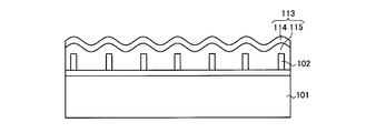
- 22 to 24 are cross-sectional views schematically showing the state of another example in which the conventional surface protection tape is attached to the front surface of the wafer.
- 22 and 23 are FIGS. 11 and 1 of Patent Document 2, respectively.
- the surface protection tape 113 in the state where the surface protection tape 113 is attached to the front surface of the wafer 101 having the unevenness due to the polyimide protection film 102, the surface protection tape 113 has the unevenness due to the polyimide protection film 102. Of the polyimide protective film 102 can not be sufficiently absorbed. The unevenness of the surface protection tape 113 at this time is 80% or more of the unevenness due to the polyimide protective film 102.
- reference numerals 114 and 115 respectively denote an adhesive layer (including an intermediate layer) and a base material layer of the surface protection tape 113 (the same applies to FIGS. 23 and 24).
- the unevenness of the surface protection tape 113 is 40% of the unevenness due to the polyimide protection film 102 Only about 60% is relaxed.
- the grinding accuracy of the wafer 101 is adversely affected, and asperities that directly reflect the unevenness of the surface protection tape 113 are formed on the back side of the wafer 101. There is a problem that the thickness accuracy of the chip is reduced.
- a semiconductor device such as an IGBT having a thin device thickness is manufactured by grinding the back surface of the wafer having an uneven shape by the polyimide protective film on the front surface device side.
- a method of manufacturing a semiconductor device is provided in which the wafer thickness accuracy can be improved by attaching a surface protection tape for back grinding to the front surface of the wafer and relaxing the uneven shape on the front surface of the wafer.
- the method of manufacturing a semiconductor device has the following features.
- the pressure-sensitive adhesive layer is deformed by heating while drawing the tape in a corrugated form along the unevenness of the semiconductor wafer in a direction away from the front surface of the semiconductor wafer to deform the corrugated sheet.
- an outer periphery of each chip is formed on the front surface of the semiconductor wafer such that the device forming region of each chip to be divided later becomes a recess.
- Grid-shaped convex portions along the surface, and in the suction heating step, the pressure-sensitive adhesive layer is deformed to absorb a step between the grid-shaped convex portions and the concave portions of the element formation region It is characterized by
- thin plate processing is performed to grind the back surface of the semiconductor wafer to make a thin wafer in a state where the tape is attached after the suction heating step.
- the method is characterized by further including a step.
- the thickness of the intermediate layer in the pressure-sensitive adhesive layer is 100 ⁇ m to 300 ⁇ m.
- the wafer front surface is heated by heating the tape for back grinding attached to the front surface of the wafer (semiconductor wafer) in a direction away from the front surface of the wafer while sucking it.
- the tape is attached to the tape
- the excess air remaining between the adhesive layer of the tape and the wafer front surface becomes small air bubbles, which are generated in the depressions on the wafer front surface and deformed by the air bubbles.
- the adhesive layer fills in the recesses on the front surface of the wafer.
- the unevenness on the front surface of the wafer is alleviated, and the surface of the tape can be planarized more than before. For this reason, it is possible to reduce the variation in wafer thickness after the grinding process on the back surface of the wafer.
- a semiconductor device such as an IGBT having a thin device thickness by grinding the back surface of a wafer having a concavo-convex shape with a polyimide protective film on the front surface device side.
- the unevenness of the surface protection tape surface for back grinding stuck to the front surface can be alleviated, and the wafer thickness accuracy can be improved.
- FIG. 10 is a cross sectional view schematically showing a configuration along a cutting line AA in FIG. 9; It is sectional drawing which shows typically the state which affixed the surface protection tape on the wafer front surface. It is sectional drawing which shows typically a mode at the time of the suction heating start of the surface protection tape stuck on the wafer front surface. It is sectional drawing which shows typically a mode after the suction heating process of the surface protection tape stuck on the wafer front surface. It is sectional drawing which shows typically the state after grinding of a wafer back surface.
- FIG. 10 is an enlarged plan view showing a part of the front surface of the wafer shown in FIG. 9;
- Embodiment 1 to 8 are cross-sectional views for explaining a method of manufacturing a semiconductor device according to the embodiment of the present invention.
- a semiconductor device semiconductor device
- n-channel IGBT having a field stop (FS) structure using an n-type wafer semiconductor wafer
- FS field stop
- the surface of the wafer on which the surface element structure portion is formed is referred to as the wafer front surface, and the surface on the opposite side is referred to as the wafer back surface.
- the detailed configuration of the surface element structure is not shown in FIGS. 1 to 8.
- a gate oxide film such as SiO 2 and a gate electrode made of polysilicon or the like are deposited on the front surface of the wafer 1 and processed.
- an interlayer insulating film such as BPSG is deposited on the surface and processed to fabricate an insulated gate structure.
- ap + base layer is selectively formed in the surface layer on the front surface of the wafer 1, and an n + emitter layer is selectively formed inside the p + base layer.
- a surface electrode made of an aluminum-silicon film or the like, that is, an emitter electrode is formed in contact with the p + base layer and the n + emitter layer.
- an insulating protection film such as polyimide is laminated on the area along the dicing line of the area surrounded by the grid-like dicing line, that is, the area on the outer periphery of the area to be a semiconductor chip.
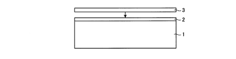
- the surface element structure 2 is completed on the front surface of the wafer 1 (FIG. 1).
- the thickness of the entire wafer 1 including the surface element structure portion 2 at this time is, for example, 500 ⁇ m.
- the illustration of the step between the insulating protection film and the emitter electrode is omitted.
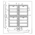
- FIG. 9 is a plan view schematically showing a polyimide protective film formed on the front surface of the wafer.
- FIG. 10 is a cross-sectional view schematically showing a configuration taken along line AA in FIG.
- the grid-like thick solid line in the wafer 1 is the polyimide protective film 11, and a plurality of rectangular regions surrounded by the polyimide protective film 11 extending in the vertical and horizontal directions are the element forming regions 12 of the individual chips.
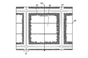
- FIG. 25 is a plan view showing a part of the front surface of the wafer shown in FIG. 9 in an enlarged manner.
- the element formation region of each chip is partitioned by dicing lines 51, and a polyimide protective film 52 is formed on the outer peripheral portion of the element formation region of the chip.
- the insulating protective film 53 such as polyimide may be formed on the gate runner.
- FIGS. 25 (b) and 25 (c) are cross-sectional views schematically showing the configuration at cutting line AA and cutting line BB in FIG. 25 (a), respectively.
- no polyimide protective film is formed on the dicing line 51.
- the width w11 of the dicing line 51 is, for example, about 80 ⁇ m, and the polyimide protective film 52 is formed in proximity to each other with the dicing line 51 interposed therebetween.
- the polyimide protective film 11 shown in FIG. 10 schematically shows the polyimide protective film 52 formed close to each other as shown in FIGS. 25 (b) and 25 (c). In FIG. 10, the insulating protective film 53 formed on the gate runner is not shown.
- the width w12 of the polyimide protective film 52 increases as the device withstand voltage increases, and is, for example, about 600 ⁇ m at a withstand voltage of 1200 V.
- the width w12 of the polyimide protective film 52 is, for example, about 100 ⁇ m at a low withstand voltage of 600 V or less, about 300 ⁇ m at a withstand voltage of 600 V, and about 1300 ⁇ m in a reverse blocking (RB) device having a withstand voltage of 1200 V.
- RB reverse blocking
- each element formation region 12 is, for example, about several mm to 20 mm square.
- the polyimide protective film 11 protrudes from the aluminum-silicon film 13 on the front surface of the wafer 1 at a height of, for example, about 10 ⁇ m to 20 ⁇ m. That is, the element formation region 12 is provided so as to be a plurality of concave portions surrounded by the grid-like convex portions made of the polyimide protective film 11. Then, on the front surface of the wafer 1, there are formed asperities composed of grid-like convex portions made of the polyimide protective film 11 and a plurality of concave portions surrounded by the convex portions.
- the surface protection tape 3 is composed of, for example, a base layer made of a hard resin material such as PET (polyethylene terephthalate) and a pressure-sensitive adhesive layer (including an intermediate layer) adhered to the front surface of the wafer 1.
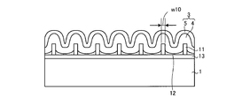
- FIG. 11 is a cross-sectional view schematically showing a surface protection tape attached to the front surface of the wafer.
- the surface of the surface protection tape 3 has a corrugated shape along the unevenness due to the polyimide protective film 11.
- the unevenness of the surface of the surface protective tape 3 appears more prominently as the width w10 of the convex portion by the polyimide protective film 11 becomes wider.
- Reference numerals 4 and 5 denote an adhesive layer (including an intermediate layer) and a base material layer of the surface protective tape 3, respectively.
- the pressure-sensitive adhesive layer 4 is composed of a pressure-sensitive adhesive layer adhered to a wafer, and an intermediate layer provided between the base material layer 5 and the pressure-sensitive adhesive layer.
- the middle layer is made of a material that expands by heating, and has fluidity by heating.
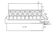
- FIG. 12 is a cross-sectional view schematically showing the start of suction and heating of the surface protection tape attached to the wafer front surface.
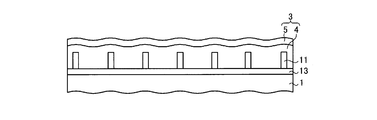
- FIG. 13 is a cross-sectional view schematically showing the appearance of the surface protection tape attached to the wafer front surface after the suction heating process.
- the flat plate-like stage 21 on which the wafer 1 is placed has a plurality of vent holes 22 for vacuum suction on the surface on which the wafer 1 is placed (hereinafter referred to as the upper surface).
- the vents 22 are connected by a pipe 23 provided inside the stage 21 and connected to suction means (not shown) such as a vacuum pump (vacuum device) via a valve (not shown).
- suction means such as a vacuum pump (vacuum device)
- a valve not shown
- the air on the upper surface side of the stage 21 is sucked by vacuum suction by the suction unit.
- the stage 21 includes heating means 24 such as a heater for heating the stage 21.
- the wafer 1 is placed on such a stage 21 with the surface protection tape 3 side being the stage 21 side. Since the surface protection tape 3 is in a corrugated form along the unevenness due to the polyimide protection film 11, the state in which the portion protruding along the projections due to the polyimide protection film 11 is in contact with the stage 21 become. In this state, vacuum suction is performed by the suction unit, and the surface protection tape 3 is sucked toward the stage 21 through the vent holes 22 and the pipe 23. Further, the surface protection tape 3 is suctioned toward the stage 21, and at the same time, the surface protection tape 3 is heated by the stage 21 heated by the heating means 24.
- the surface protection tape before heating is heated by suctioning the surface protection tape 3 toward the stage 21 in this way.
- the bubbles existing between the pressure-sensitive adhesive layer 4 and the irregularities on the front surface of the wafer 1 become a plurality of small bubbles and are generated in the intermediate layer of the surface protection tape 3 to be in the element formation region 12 And the recesses in the front surface of the wafer 1 are filled. Therefore, as shown in FIG. 13, the unevenness of the surface of the base material layer 5 of the surface protection tape 3 gradually becomes smaller, and finally, for example, 20% or less of the height of the unevenness of the front surface of the wafer 1 It becomes height. That is, since the middle layer in the pressure-sensitive adhesive layer 4 has fluidity, the surface protection tape 3 is flattened by the generation of a plurality of small air bubbles scattered in the middle layer.
- FIG. 14 is a cross-sectional view schematically showing a state after grinding on the back surface of the wafer.
- the surface protection tape 3 is peeled off from the surface of the surface element structure 2 using, for example, a general tape peeling device to remove the surface protection tape 3. Then, spin grinding or dip etching is performed on the ground surface of the wafer 1 to remove the fractured layer formed on the ground surface. Thereby, the thickness of the whole wafer 1 including the surface element structure portion 2 becomes, for example, a thickness of 80 ⁇ m.
- boron which is a p-type impurity
- the rear surface of the wafer 1 is annealed by laser irradiation or the like to form ap + layer 6 to be a collector layer.
- a plurality of metals such as aluminum, titanium, nickel and gold are vapor-deposited on the back surface of the wafer 1 to form a back surface electrode 7 to be a collector electrode.
- a general dicing tape 8 is attached to the back surface of the wafer 1 to invert the wafer 1.
- the semiconductor device according to the embodiment is completed by cutting the wafer 1 into a plurality of chips 9.
- each chip 9 is soldered to a fixing member such as a wiring board via the back surface electrode 7.
- an aluminum wire electrode is fixed to the electrode on the front surface side of each chip 9 by an ultrasonic wire bonding apparatus.
- FIG. 15 is a characteristic diagram showing asperities on the surface of the surface protective tape immediately before grinding in the first embodiment.
- FIG. 16 is a characteristic diagram showing the wafer thickness (chip thickness) after the grinding process of the first embodiment.
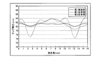
- the wafer thickness was measured using a transmission infrared laser (the same applies to FIG. 17).
- the measurement length is the length of the cutting line across the opposite side of the convex portion of the polyimide protective film which encloses one element formation region in a rectangular shape, and the same portion of the wafer is measured in FIGS.
- the first example flattens the surface of the surface protection tape 3 by heating while suctioning the surface protection tape 3 attached to the front surface of the wafer 1 according to the method of manufacturing a semiconductor device according to the embodiment. After that, the backside of the wafer 1 is ground.
- the thicknesses of the pressure-sensitive adhesive layer (including the intermediate layer) 4 and the substrate layer 5 are 215 ⁇ m (adhesive layer: 20 ⁇ m, intermediate layer 195 ⁇ m) and 50 ⁇ m, respectively.
- the chip size was 9.7 mm ⁇ 9.7 mm, and the width w12 of the polyimide protective film 52 formed in one element formation region 12 was 600 ⁇ m, which is a thickness corresponding to an IGBT with a withstand voltage of 1200 V. That is, when the polyimide protective film 52 adjacent to the adjacent element forming region 12 with the dicing line 51 interposed therebetween is regarded as one convex portion, the width of the convex portion formed by the polyimide protective film 52 adjacent to each other sandwiching the dicing line 51 w10 is about 1200 ⁇ m.
- FIGS. 15 and 16 show the first and second conventional examples as a comparison together with the first embodiment.
- the first conventional example after the surface protection tape is attached to the front surface of the wafer, grinding processing is performed on the back surface of the wafer.
- the second conventional example after the surface protection tape is attached to the front surface of the wafer, the surface of the surface protection tape is flattened by heat treatment in a furnace, and then the wafer back surface is ground. There is.
- the conditions other than the process from the application of the surface protection tape to the grinding process on the back surface of the wafer in the first and second conventional examples are the same as in the first embodiment.
- the convex portion (measurement with a polyimide protective film having a thickness of about 10 .mu.m surrounding the element formation region only when the surface protective tape is attached to the front surface of the wafer as in the first conventional example) It has been confirmed that the surface protection tape becomes corrugated along the length of 3 mm and around 13 mm). Further, in the first conventional example, the surface protection tape is also formed by the convex portion (measurement length 6 mm and 9 mm vicinity) of the insulating protective film having a thickness of about 10 ⁇ m such as polyimide for protecting the gate runner provided in the element formation region. Has been confirmed to be corrugated. That is, in the first conventional example, it was confirmed that the alleviating performance against unevenness by the polyimide protective film and the insulating protective film for protecting the gate runner is both low.
- the alleviation performance against irregularities due to the polyimide protective film can be improved as compared with the first conventional example, but the gate runner is It was confirmed that the alleviating performance against irregularities due to the insulating protective film to be protected is low.
- the alleviation performance against irregularities by the polyimide protective film and the insulating protective film 53 for protecting the gate runner is both higher than that of the first conventional example, and the irregularities on the surface of the surface protection tape 3 are about 2 ⁇ m in the chip surface. It has been confirmed that it can be most flattened.
- the relaxation performance of the unevenness on the front surface of the wafer is different, the unevenness due to the insulating protective film protecting the gate runner more than the relaxation performance for the unevenness by the polyimide protective film It was confirmed that the relaxation performance against was higher. Since both the polyimide protective film and the insulating protective film protecting the gate runner are formed with a thickness of about 10 ⁇ m, the width of the convex portion by the insulating protective film protecting the gate runner is the convex portion by the polyimide protective film It is because it is narrower than the width of. For this reason, it was confirmed that the relief performance of the unevenness of the surface of the surface protection tape is lowered as the width of the convex portion generated by the polyimide on the wafer front surface is wider.
- the chip thickness becomes thinner at portions corresponding to the convex portions on the surface protection tape surface. It was confirmed that the chip thickness is thicker at the portion corresponding to the recess, but the smaller the unevenness of the surface protection tape surface is, the smaller the variation of the chip thickness becomes. Therefore, in the first embodiment in which the surface protection tape surface is the most flat, just before grinding on the back surface of wafer 1, the variation in thickness of chip 9 after grinding on the back surface of wafer 1 is smallest, and 2 ⁇ m in the surface of chip 9. It has been confirmed that the degree can be reduced.
- FIG. 17 is a characteristic diagram showing the wafer thickness (chip thickness) after the grinding process of the second embodiment.
- the second embodiment and the third and fourth prior art shown in FIG. 17 are manufactured by the same method as the first embodiment and the first and second prior art except using a thin surface protection tape having a thickness of 165 ⁇ m. There is.
- the thickness of the pressure-sensitive adhesive layer (including the intermediate layer) and the substrate layer in the surface protection tape having a thickness of 165 ⁇ m is 140 ⁇ m (adhesive layer: 20 ⁇ m, intermediate layer 120 ⁇ m) and 25 ⁇ m, respectively.
- the surface is not only performed in the third conventional example in which nothing is performed after applying the surface protective tape, but also in the fourth conventional example in which the surface protection tape is heated in a furnace.
- the surface of the protective tape was not substantially flattened, and as shown in FIG. 17, the variation in chip thickness after grinding on the back of the wafer was not improved.
- the variation in the thickness of the chip 9 after grinding on the back surface of the wafer 1 is reduced even if it does not reach the first embodiment using the surface protection tape 3 with a thickness of 265 ⁇ m. That was confirmed.
- FIG. 18 is a conceptual diagram schematically showing the state of air bubbles on the front surface of the wafer before the heat treatment of the first embodiment.
- FIG. 19 is a conceptual diagram schematically showing the state of air bubbles on the front surface of the wafer after the suction heating process of the first embodiment.
- FIG. 20 is a conceptual diagram schematically showing the state of air bubbles on the front surface of the wafer after the heat treatment of the second conventional example.
- Arrows C1 and C2 for cutting the wafer in FIGS. 19 and 20 are measurement lines when the unevenness of the surface protection tape shown in FIG. 15 is measured in the first embodiment and the second conventional example, respectively.
- air bubbles hatching in the vicinity of the convex portion by the polyimide protective film 11 between the surface protection tape 3 attached to the wafer 1 front surface and the wafer 1 front surface before heating.
- the part shown by) 31 remains a lot.
- the surface protection tape 3 attached to the front surface of the wafer 1 is heated while being suctioned, as shown in FIG. 19, the pressure-sensitive adhesive layer 4 of the surface protection tape 3 before heating and the wafer 1 front surface. It was confirmed that the air bubbles 31 existing between the surface and the surface became a plurality of small air bubbles 32 and were uniformly scattered in the surface of the element formation region 12.
- the small bubbles 32 absorb the step caused by the unevenness due to the polyimide protection film 11 (polyimide protection film 52) and the insulation protection film 53 protecting the gate runner, and the unevenness on the surface of the surface protection tape 3 is alleviated.
- the unevenness of the surface of the surface protection tape 3 is alleviated also for the step due to the insulating protective film 53 such as polyimide formed on the gate runner.
- the state of air bubbles on the front surface of the wafer before heat treatment is the same as in the first embodiment (air bubbles 31 in FIG. 18), and the air bubbles are small air bubbles after heat treatment in the furnace.
- the point to become was the same as that of the first embodiment.
- small bubbles 33 generated after the heat treatment are scattered in the vicinity of the polyimide protective film 41, so that the surface of the surface protective tape in the vicinity of the convex portion by the polyimide protective film 41. It was confirmed that the unevenness was alleviated.
- reference numerals 43 and 44 denote gate runners and dicing lines, respectively.
- the mechanical strength of the wafer 1 is reduced. For this reason, it is preferable not to concentrate the air bubbles in one or more places. That is, it is better to make the large air bubbles 31 shown in FIG. 18 smaller and make the air bubbles 31 evenly dispersed in the surface of the element formation region 12 as in the plurality of small air bubbles 32 and 33 shown in FIGS. Since the intermediate layer around the air bubbles can cover (relax) the decrease in mechanical strength of the wafer 1 due to the air bubbles due to the small air bubbles, the decrease in mechanical strength of the wafer 1 is suppressed.
- the intermediate layer in the pressure-sensitive adhesive layer 4 has fluidity, and a plurality of small air bubbles 32 are generated in the intermediate layer, whereby the surface protection tape 3 is flattened.
- the thickness of the intermediate layer in the adhesive layer 4 is preferably 100 ⁇ m or more.
- the thickness of the intermediate layer in the pressure-sensitive adhesive layer 4 is more preferably 100 ⁇ m or more and 300 ⁇ m or less.
- the surface protection tape attached to the front surface of the wafer is suctioned and heated to attract the surface protection tape onto the front surface of the wafer.
- the excess air remaining between the adhesive layer of the protective tape and the front surface of the wafer is generated as small air bubbles in the recess of the front surface of the wafer, and the adhesive layer deformed by the air bubbles causes the wafer to be cleaned.
- the recess on the front side is filled.
- the thin surface protection tape (surface protection tape with a thin intermediate layer thickness) can be obtained. Even when it is used, the thickness accuracy of the chip can be improved. Therefore, the cost of the surface protection tape itself can be reduced.
- a punch-through (PT) type, non-punch-through (NPT) type, field stop (FS) type IGBT, or a diode such as FWD (Free Wheeling Diode) can be manufactured by the manufacturing process of the present invention.
- the surface element structure of the IGBT may be planar or trench.
- the surface protection tape is peeled off after grinding the wafer and the subsequent steps are performed.
- the surface protection tape has high acid resistance, carbon in high vacuum, etc.
- the subsequent steps may be performed without peeling off the surface protection tape after grinding processing of the wafer.
- the wafer 1 is placed on the stage 21 heated by the heater, but the positional relationship between the wafer 1 and the stage 21 in the upper and lower directions is reversed.
- the stage 21 may be located. In this case, the surface protection tape 3 attached to the front surface of the wafer is heated while being sucked from above the wafer 1.
- the present invention is not limited to an IGBT in which the thickness of the wafer (including the thickness of the surface element structure portion) after grinding processing is 100 ⁇ m, and has a step of grinding the wafer back surface to make the wafer thickness 100 ⁇ m or less
- the present invention can be applied to a method of manufacturing a semiconductor element for power.
- the method of manufacturing a semiconductor device according to the present invention is useful for manufacturing a semiconductor device having a thin device thickness, and in particular, a general-purpose inverter, AC servo, uninterruptible power supply (UPS) or switching power supply etc. It is suitable for manufacturing power semiconductor devices such as IGBTs used in the industrial field, and in the field of consumer electronics such as microwave ovens, rice cookers or strobes.
Landscapes
- Engineering & Computer Science (AREA)
- Mechanical Engineering (AREA)
- Mechanical Treatment Of Semiconductor (AREA)
- Container, Conveyance, Adherence, Positioning, Of Wafer (AREA)
Abstract
ウェハおもて面のポリイミド保護膜による凹凸によってバックグラインド用の表面保護テープに生じた凹凸を緩和し、ウェハ裏面の研削加工によるウェハの厚さ精度を向上させ、チップ厚さのばらつきを低減すること。ウェハ(1)のポリイミド保護膜(11)による凹凸を有するおもて面に、基材層(5)と粘着剤層(中間層を含む)(4)を備えた表面保護テープ(3)を貼り付ける。次に、表面保護テープ(3)側をステージ(21)側にしてウェハ(1)をステージ(21)に載置した後、表面保護テープ(3)をステージ(21)側へ吸引しながら加熱することによって表面保護テープ(3)の表面を平坦化する。次に、ウェハ(1)裏面を研削加工して薄ウェハにした後、ウェハ(1)裏面に裏面素子構造を形成し、ダイシングをおこなってチップに切断する。
Description
この発明は、半導体素子の製造方法に関する。
従来、コンピュータや通信機器の主要部分には、多数のトランジスタや抵抗等を、電気回路を構成するようにむすびつけて、1チップ上に集積した集積回路(IC)が多用されている。また、上記ICよりも高電圧・大電流のスイッチングに用いる半導体素子として電力用半導体素子がある。電力用半導体素子には、たとえば絶縁ゲート型バイポーラトランジスタ(以下、IGBTとする)やダイオードがある。
ここで、従来のIGBTの製造プロセスについて説明する。まず、ウェハのおもて面側に、ベース領域、エミッタ領域、ゲート酸化膜、ゲート電極、層間絶縁膜、エミッタ電極および絶縁保護膜よりなる表面素子構造部を形成する。エミッタ電極は、例えばアルミ・シリコン膜でできている。絶縁保護膜は、例えばポリイミド膜でできている。次に、ウェハおもて面にポリイミド保護膜を形成する。
次に、ポリイミド保護膜が形成されたウェハおもて面に表面保護テープを貼り付けてからウェハの裏面を研削し、ウェハを所望の厚さとする。次に、ウェハ裏面側にコレクタ層などを形成する。その後、ウェハの裏面、すなわちコレクタ層の表面に、アルミニウム、チタン、ニッケルおよび金などの複数の金属を蒸着し、コレクタ電極を形成する。最後に、コレクタ電極側にダイシングテープを貼り付けてダイシングをおこない、ウェハを複数のチップに切断することにより、IGBTが完成する。
一般に、従来より用いられている表面保護テープは、基材層と粘着剤層(中間層を含む)とを組み合わせた構成のものであり、例えば150μmの厚さを有する。また、表面保護テープとして、融点105℃以下のホットメルト層を少なくとも有し、半導体ウェハ表面に加熱して貼り付けられるホットメルトシートが公知である(例えば、下記特許文献1参照。)。
また、上述したようにウェハおもて面に表面保護テープを貼り付ける方法として、半導体ウェハのポリイミド保護膜による凹凸を有する表面に、基材層と粘着剤層を備えた表面保護テープを貼り付けた後に加熱し、基材層および粘着剤層を変形させて、基材層の表面をほぼ平坦にする方法が提案されている(例えば、下記特許文献2参照。)。
また、別の方法として、次の方法が提案されている。半導体ウェハ表面の上方に保護テープを供給し、貼付けローラで押圧しながら転動移動させて半導体ウェハの表面に当該保護テープを貼付け、貼付けられた保護テープを半導体ウェハの外周に沿って切断する。その後に加圧部材で保護テープを表面から加圧し、その表面を扁平化する(例えば、下記特許文献3参照。)。
また、別の方法として、基材と少なくとも一層以上の中間層と粘着剤層をこの順番で積層してなる半導体ウェハ保護用粘着シートを半導体ウェハの表面に貼り合わせる方法であって、粘着シートと半導体ウェハの貼り合わせ温度が50℃~100℃であり、粘着剤層と接する側の中間層の貼り合わせ温度における損失正接(tanδ)が0.5以上である方法が提案されている(例えば、下記特許文献4参照。)。
また、別の方法として、ワークを載置する載置手段を加熱手段で加熱する加熱工程と、載置手段にワークを載置した状態で、載置手段およびワークを内在させかつ内部を密封状態で閉塞可能な圧力室を、吸引手段を用いて真空吸引をおこなう吸引工程と、真空度に到達したことを検出した後に、テープ部材に対してワークを近付けて、ワークをテープ部材に接着させる接着工程と、接着工程における接着を予め設定された時間だけ実行した後に、加圧手段を作動させて圧力室の内部に空気を加圧状態で導入する加圧工程と、を含む方法が提案されている(例えば、下記特許文献5参照。)。
しかしながら、上述した製造プロセスのように、ウェハ裏面を研削する前にウェハおもて面にポリイミド保護膜を形成する場合、次のような種々の不具合が生じる。図21は、従来の表面保護テープをウェハおもて面に貼り付けた状態を模式的に示す断面図である。例えば、表面素子構造部を保護するポリイミド保護膜102は、ウェハ101に作製された複数のチップの素子形成領域を囲むように各チップの外周に沿って形成される。
すなわち、図21に示すように、ウェハ101のおもて面には、ポリイミド保護膜102が形成されている。ポリイミド保護膜102はウェハ101のおもて面に凸状に形成される。このポリイミド保護膜102は、ダイシングラインによって格子状に区画された領域の内側で、ダイシングラインに沿って設けられている。そして、ポリイミド保護膜102によって凸状となる部分(以下、凸状部とする)と、この凸状部に囲まれた凹部が形成されるため、ウェハ101のおもて面には、凹凸が複数形成されている。この凹凸による段差の高さは、10μm~20μm程度であり、凹部の大きさは、数mm~20mm角程度である。一方、従来の表面保護テープ103は、150μm程度と厚さが薄く、数μm程度の高さの段差に対する緩和性能しか有していない。
従って、ウェハ101のおもて面に従来の表面保護テープ103を貼り付けても、ポリイミド保護膜102による凹凸に沿って貼り付いてしまい、ウェハ101のおもて面には、ポリイミド保護膜102によりウェハ101おもて面に生じた段差の約95%程度の高さの段差が残ってしまう。そのため、ウェハ101裏面の研削加工中に、ウェハ101おもて面のポリイミド保護膜102よりなる格子状の凸状部に囲まれる凹部に形成される表面素子構造部(主にエミッタ電極を構成するアルミ・シリコン膜)が研削砥石によってウェハ101裏面側から押され変形した状態で研削加工が進行することになる。
従って、ポリイミド保護膜102による凹凸が大きい場合、ウェハ101おもて面の凹部に大きな応力がかかり、ウェハ101裏面の研削加工をおこなっただけでもウェハ101が破損することがある。また、ウェハ101が破損しなかったとしても、ウェハ101おもて面の凹部に応力がかかった状態でウェハ101裏面の研削加工がおこなわれることで、凹部が設けられている部分のウェハ101の厚さがポリイミド保護膜102よりなる凸状部が設けられている部分のウェハ101の厚さよりも厚くなってしまう。
例えば、ダイシングラインによって区画された矩形状の各チップの外周に沿って100μm~500μm程度の幅でポリイミド保護膜102を形成する。このとき、ポリイミド保護膜102よりなる凸状部が設けられている部分のウェハ101の厚さが100μmになるまでウェハ101裏面の研削加工をおこなった場合、ポリイミド保護膜102による凸状部に囲まれた凹部のウェハ101の厚さ、すなわちチップ中央部の厚さは110μm程度になってしまう。この場合、100μmのウェハ厚さで設計したチップの耐圧は得られるが、ウェハ101中央部の厚さが110μmとなっている分だけ電気的損失が生じる。逆に、凹部のウェハ101の厚さが100μmになるまでウェハ101裏面の研削加工をおこなった場合、ポリイミド保護膜102によって凸状となるチップ外周部の厚さが過剰に薄くなり、通電時に素子破壊が起こる虞がある。
このような問題を解決する方法として、次のような方法が提案されているが、それぞれ技術的課題が多い。例えば、接着剤や厚さの厚い両面テープなどにより高剛性基板とウェハとを貼り合わせる方法が提案されている。しかし、高剛性基板を再利用するためにかかる材料費などが高額となり、さらに高剛性基板をウェハに貼り合わせるための周辺装置が多数必要となるなどコスト的な問題が生じる。また、ウェハ裏面の研削加工をおこなうときのウェハの厚さ精度を向上させるための張り合わせ技術が必要となる。
また、表面保護テープ自体を厚くしてウェハおもて面の凹凸を埋め込むことで、ウェハおもて面の凹凸に対する緩和性能を高めた各種テープ(主に半田バンプによる凹凸を対象とした保護テープ)が開発されている。しかし、テープの厚さが500μm程度と厚いため、半田バンプのように点在する凸部よりなる凹凸を埋め込む作用はあるが、チップ外周のライン上に存在する格子状の高い凹凸に対する埋め込み性能はあまり高くない。このため、ウェハ裏面の研削加工後のウェハの厚さ精度も数倍悪くなってしまう。
また、ポリイミド保護膜よりなる格子状の凸状部に囲まれる凹部を狭くすることにより、ウェハおもて面のポリイミド保護膜による凹凸自体をなくす方法が提案されている。しかし、ポリイミド保護膜によるウェハへの応力が大きくなりすぎるため、ウェハを薄くしたときにウェハの反りが非常に大きくなり、運搬が困難になるという問題がある、また、エミッタ電極の露出面積が小さくなるため、装置を組み立てる上での制約が増えてしまう。さらに、エミッタ電極の露出面積が少なくなることで、めっきにより成膜される配線とエミッタ電極との実質的な接合面積が小さくなり、放熱性が低下する。
また、上記特許文献1に開示されたホットメルトシートは、ウェハおもて面の凹凸によく追従して、ウェハと保護保持用シートとが隙間なく接着され、ウェハ裏面の研削加工時における、ウェハパターン面への研削水や異物の浸入、加工ミス、ディンプルの発生、ウェハ割れなどを防ぐためのものである。
また、上記特許文献1には、バンプが点在するウェハに対してホットメルトシートを貼り付けた実施例が開示されているが、ダイシングラインによって格子状に区画された領域の内側でダイシングラインに沿って設けられたポリイミド保護膜よりなる凸状部と数mm~20mm角程度の凹部とからなる凹凸による段差を緩和することについては、何ら記載されていない。従って、このような大きな凹部と高い凸部を有するウェハおもて面に上記特許文献1のホットメルトシートを貼り付けても、平坦なシート表面が得られるか否かは不明である。
また、上記特許文献2には、200μm以上の厚さの特殊な表面保護テープをウェハおもて面に貼り付けた後、炉内で表面保護テープを加熱しポリイミド保護膜による凹凸を緩和させる実施例が開示されている。しかし、上記特許文献2では、ポリイミド保護膜による凹凸の緩和性能が足りず、ウェハの平坦性が悪くなる虞がある。図22~24は、従来の表面保護テープをウェハおもて面に貼り付けた別の一例の状態を模式的に示す断面図である。図22,23は、上記特許文献2の図11,1である。
具体的には、図22に示すように、ウェハ101のポリイミド保護膜102による凹凸を有するおもて面に表面保護テープ113を貼り合せた状態では、表面保護テープ113がポリイミド保護膜102による凹凸に沿って波板状になり、ポリイミド保護膜102による凹凸を十分に吸収することができない。このときの表面保護テープ113の凹凸は、ポリイミド保護膜102による凹凸の80%以上である。図22において、符号114および符号115は、それぞれ表面保護テープ113の粘着剤層(中間層を含む)および基材層である(図23,24においても同様)。
その後、図23に示すように、炉内で表面保護テープ113を加熱してポリイミド保護膜102による凹凸を緩和させたとしても、表面保護テープ113の凹凸はポリイミド保護膜102による凹凸の40%~60%程度にしか緩和されない。この状態でウェハ101裏面の研削加工をおこなった場合、図24に示すように、ウェハ101の研削精度に悪影響を及ぼし、表面保護テープ113の凹凸をそのまま反映した凹凸がウェハ101裏面に生じるため、チップの厚さ精度が低下するという問題が生じる。
また、上記特許文献3~5のようにウェハのおもて面に貼り付けた表面保護テープを加圧および加熱することで平坦化する方法では、表面デバイスの表面素子構造部による複数の凸部に対する緩和性能は有しているが、ポリイミド保護膜よりなる格子状の凸状部に対して十分な緩和性能を発揮することができない。従って、上記特許文献3~5においても、ウェハ裏面の研削加工をおこなったときに、表面保護テープの凹凸に対応した凹凸がウェハ101裏面に生じるため、チップの厚さ精度が低下するという問題が生じる。
この発明は、上述した従来技術による問題点を解消するため、おもて面デバイス側にポリイミド保護膜による凹凸形状を有するウェハの裏面を研削してデバイス厚の薄いIGBT等の半導体素子を製造するにあたって、ウェハおもて面にバックグラインド用の表面保護テープを貼り付けてウェハおもて面の凹凸形状を緩和することによってウェハ厚さ精度を向上させることができる半導体素子の製造方法を提供することを目的とする。
上述した課題を解決し、目的を達成するため、この発明にかかる半導体素子の製造方法は、次の特徴を有する。まず、半導体ウェハの凹凸を有するおもて面に、基材層と粘着剤層を備えたテープを、前記粘着剤層が前記半導体ウェハのおもて面に接するように貼り付ける貼り付け工程をおこなう。次に、前記半導体ウェハの凹凸に沿って波板状になった前記テープを前記半導体ウェハのおもて面から離れる方向に吸引しながら加熱することによって前記粘着剤層を変形させ、波板状の前記基材層の表面をほぼ平坦にする吸引加熱工程をおこなう。
また、この発明にかかる半導体素子の製造方法は、上述した発明において、前記半導体ウェハのおもて面には、後に分割される個々のチップの素子形成領域が凹部となるように各チップの外周に沿う格子状の凸状部が設けられており、前記吸引加熱工程では、前記粘着剤層を、格子状の前記凸状部と前記素子形成領域の前記凹部との段差を吸収するように変形させることを特徴とする。
また、この発明にかかる半導体素子の製造方法は、上述した発明において、前記吸引加熱工程後に、前記テープを貼り付けた状態のまま、前記半導体ウェハの裏面を研削加工して薄ウェハにする薄板加工工程をさらに含むことを特徴とする。
また、この発明にかかる半導体素子の製造方法は、上述した発明において、前記粘着剤層における中間層の厚さが100μm以上300μm以下であることを特徴とする。
上述した発明によれば、ウェハ(半導体ウェハ)のおもて面に貼り付けたバックグラインド用のテープをウェハのおもて面から離れる方向に吸引しながら加熱することによって、ウェハおもて面にテープを貼り付けたときにテープの粘着剤層とウェハおもて面との間に残った余分な空気が小さな気泡となってウェハおもて面の凹部内に発生し、この気泡によって変形した粘着剤層によってウェハおもて面の凹部が埋められる。これにより、ウェハおもて面の凹凸が緩和され、テープの表面を従来よりも平坦化することができる。このため、ウェハ裏面の研削加工後におけるウェハ厚さのばらつきを小さくすることができる。
本発明にかかる半導体素子の製造方法によれば、おもて面デバイス側にポリイミド保護膜による凹凸形状を有するウェハの裏面を研削してデバイス厚の薄いIGBT等の半導体素子を製造するにあたって、ウェハおもて面に貼り付けたバックグラインド用の表面保護テープ表面の凹凸を緩和し、ウェハ厚さ精度を向上させることができるという効果を奏する。
以下に添付図面を参照して、この発明にかかる半導体素子の製造方法の好適な実施の形態を詳細に説明する。なお、以下の実施の形態の説明および添付図面において、同様の構成には同一の符号を付し、重複する説明を省略する。
(実施の形態)
図1~8は、本発明の実施の形態にかかる半導体素子の製造方法を説明するための断面図である。特に限定しないが、ここでは、n型のウェハ(半導体ウェハ)を用いてフィールドストップ(FS)構造のnチャネル型IGBTを作製(製造)する場合を例にして説明する。ウェハの、表面素子構造部が形成される側の面をウェハおもて面とし、その反対側の面をウェハ裏面とする。なお、図1~8においては、表面素子構造部の詳細な構成の図示を省略する。
図1~8は、本発明の実施の形態にかかる半導体素子の製造方法を説明するための断面図である。特に限定しないが、ここでは、n型のウェハ(半導体ウェハ)を用いてフィールドストップ(FS)構造のnチャネル型IGBTを作製(製造)する場合を例にして説明する。ウェハの、表面素子構造部が形成される側の面をウェハおもて面とし、その反対側の面をウェハ裏面とする。なお、図1~8においては、表面素子構造部の詳細な構成の図示を省略する。
ウェハ1のおもて面の製造プロセスの一例を説明する。まず、ウェハ1のおもて面にSiO2等のゲート酸化膜とポリシリコン等からなるゲート電極を堆積し、これらを加工する。そして、その表面にBPSG等の層間絶縁膜を堆積し、これを加工することによって、絶縁ゲート構造を作製する。次に、ウェハ1おもて面の表面層にp+ベース層を選択的に形成し、p+ベース層の内部にn+エミッタ層を選択的に形成する。
次に、p+ベース層およびn+エミッタ層に接するようにアルミ・シリコン膜等からなる表面電極、すなわちエミッタ電極を形成する。そして、格子状のダイシングラインに囲まれた領域のダイシングラインに沿った領域、すなわち、半導体チップとなる領域の外周の領域にポリイミド等の絶縁保護膜を積層する。ここまでで、ウェハ1おもて面に表面素子構造部2ができあがる(図1)。このときの表面素子構造部2を含めたウェハ1全体の厚さは、例えば500μmである。なお、図1では、絶縁保護膜とエミッタ電極との段差の図示は省略している。
ここで、ウェハ1おもて面にポリイミド保護膜が形成された様子を図9,10に模式的に示す。図9は、ウェハおもて面にポリイミド保護膜が形成された様子を模式的に示す平面図である。図10は、図9の切断線A-Aにおける構成を模式的に示す断面図である。図9において、ウェハ1内の格子状の太い実線がポリイミド保護膜11であり、縦横に伸びるポリイミド保護膜11により囲まれる複数の矩形領域は、個々のチップの素子形成領域12である。
このチップの素子形成領域12付近を拡大した様子を図25に一例として示す。図25は、図9に示すウェハおもて面の一部を拡大して示す平面図である。図25(a)に示すように、個々のチップの素子形成領域は、ダイシングライン51によって区画されており、チップの素子形成領域の外周部分にポリイミド保護膜52が形成されている。また、チップの素子形成領域にゲートランナーが形成されている場合は、ゲートランナー上にもポリイミド等の絶縁保護膜53が形成される場合もある。
図25(b),25(c)は、それぞれ図25(a)の切断線A-A、切断線B-Bにおける構成を模式的に示す断面図である。図25に示すように、この例では、ダイシングライン51上にはポリイミド保護膜は形成されていない。ダイシングライン51の幅w11は、例えば80μm程度であり、ダイシングライン51を挟んでポリイミド保護膜52が近接して形成されることになる。図10に示すポリイミド保護膜11は、図25(b),25(c)に示すように近接して形成されたポリイミド保護膜52を模式的に示したものである。なお、図10において、ゲートランナー上に形成された絶縁保護膜53については図示を省略している。
ポリイミド保護膜52の幅w12は、素子耐圧が高くなるほど広くなり、例えば、耐圧1200Vで600μm程度である。また、ポリイミド保護膜52の幅w12は、例えば、600V以下の低耐圧で100μm程度であり、耐圧600Vで300μm程度であり、耐圧1200Vの逆阻止(RB:Reverse Blocking)デバイスで1300μm程度である。ダイシングライン51を挟んで隣り合うポリイミド保護膜52を1つの凸状部と見なす場合、この凸状部の幅w10(すなわち図10に示すポリイミド保護膜11による凸状部の幅w10)は、ポリイミド保護膜52の幅w12の2倍程度の寸法となり、例えば、耐圧1200Vで1200μm程度となる。
図10に示すように、各素子形成領域12の大きさは、例えば数mm~20mm角程度である。また、ポリイミド保護膜11は、ウェハ1おもて面のアルミ・シリコン膜13から例えば10μm~20μm程度の高さで突出している。すなわち、ポリイミド保護膜11よりなる格子状の凸状部に囲まれる複数の凹部となるように素子形成領域12が設けられている。そして、ウェハ1おもて面には、ポリイミド保護膜11よりなる格子状の凸状部と、この凸状部に囲まれる複数の凹部とからなる凹凸が形成されている。
表面素子構造部2の完成後、図2に示すように、例えば一般的なテープ貼り付け装置を用いて、表面素子構造部2の表面に、バックグラインド時に表面素子構造部2を保護するための表面保護テープ3を貼り付ける。表面保護テープ3は、例えばPET(ポリエチレンテレフタレート)などの硬い樹脂材料からなる基材層と、ウェハ1おもて面に粘着される粘着剤層(中間層を含む)とで構成されている。
図11は、ウェハおもて面に表面保護テープを貼り付けた状態を模式的に示す断面図である。図11に示すように、ポリイミド保護膜11による凸状部の幅w10が広い場合、表面保護テープ3を貼り付けただけでは、その凹凸を十分に吸収しているとはいえない。このため、表面保護テープ3の表面は、ポリイミド保護膜11による凹凸に沿って波板状になる。表面保護テープ3の表面の凹凸は、ポリイミド保護膜11による凸状部の幅w10が広くなるほど顕著にあらわれる。なお、符号4および符号5は、それぞれ表面保護テープ3の粘着剤層(中間層を含む)および基材層である。粘着剤層4は、ウェハに粘着される粘着層と、基材層5と粘着層との間に設けられる中間層とからなる。中間層は、加熱することにより膨張する材質からなり、加熱することにより流動性をもつ。
そこで、半導体ウェハの凹凸に沿って波板状になっている表面保護テープ3をウェハ1おもて面から離れる方向に吸引しながら加熱する。図12は、ウェハおもて面に貼り付けた表面保護テープの吸引加熱開始時の様子を模式的に示す断面図である。図13は、ウェハおもて面に貼り付けた表面保護テープの吸引加熱処理後の様子を模式的に示す断面図である。図12に示すように、ウェハ1が載置される平板状のステージ21は、ウェハ1が載置される側の面(以下、上面とする)に真空吸引用の複数の通気孔22を所定の間隔で備える。すべての通気孔22は、ステージ21の内部に設けられた配管23で連結され、図示省略するバルブを介して真空ポンプ(真空装置)などの吸引手段(不図示)につながれている。吸引手段によって真空吸引することによって、ステージ21の上面側の空気が吸引される。また、ステージ21は、ステージ21を加熱するヒーターなどの加熱手段24を備える。
このようなステージ21上に、表面保護テープ3側をステージ21側にしてウェハ1を載置する。表面保護テープ3は、ポリイミド保護膜11による凹凸に沿って波板状になっているため、ポリイミド保護膜11による凸部に沿って突出した状態になっている部分がステージ21に接触した状態となる。この状態で吸引手段によって真空吸引し、通気孔22および配管23を介して表面保護テープ3をステージ21側に吸引する。さらに、表面保護テープ3をステージ21側に吸引すると同時に、加熱手段24によって加熱されたステージ21によって表面保護テープ3を加熱する。
表面保護テープ3をステージ21側に吸引しながら加熱することにより、表面保護テープ3の通気孔22に接している部分が通気孔22内に吸引され凸状に変形する虞があるが、通気孔22の開口幅を狭くする、ポーラスチャックを備えたステージ21を用いる、表面保護テープ3への吸引力を低くするなどによる対策が可能である。
表面保護テープ3を加熱することによって、粘着剤層4における中間層が流動性を持つので、このように表面保護テープ3をステージ21側に吸引しながら加熱することによって、加熱前の表面保護テープ3の粘着剤層4とウェハ1おもて面の凹凸との間に存在していた気泡が複数の小さな気泡となって表面保護テープ3の中間層内に発生して素子形成領域12面内に均等に散在され、ウェハ1おもて面の凹部が埋められる。従って、図13に示すように、表面保護テープ3の基材層5の表面の凹凸は徐々に小さくなり、最終的には、ウェハ1おもて面の凹凸の高さの例えば20%以下の高さとなる。すなわち、粘着剤層4における中間層が流動性を有するので、中間層内に複数の小さな気泡が散在して発生することによって、表面保護テープ3が平坦化される。
以上のようにして表面保護テープ3の表面を平坦化した後、図3に示すように、ウェハ1を反転させて、バックグラインド装置によりウェハ1裏面の研削加工をおこない、表面素子構造部2を含むウェハ1全体の厚さが所望の厚さ、例えば100μmの厚さで残るようにする。図14は、ウェハ裏面の研削加工後の状態を模式的に示す断面図である。ポリイミド保護膜11による凹凸の高さが例えば10μmである場合、上述したように表面保護テープ3を吸引しながら加熱することにより、表面保護テープ3表面の凹凸の高さを素子形成領域12面内(チップ面内)で2μm以下(=10μm×20%以下)程度にすることができる。その結果、図14に示すように、ウェハ1裏面の研削加工時にウェハ1裏面に反映されてしまう凹凸の高さを2μm以下程度に抑えることができるため、チップ面内でのシリコン厚さのばらつきを従来よりも少ない2μm以下程度に抑えることができる。従って、チップの厚さ精度が向上する。
ウェハ1を研削加工した後、図4に示すように、例えば一般的なテープ剥離装置を用いて、表面素子構造部2の表面から表面保護テープ3を剥離させて、表面保護テープ3を取り除く。そして、ウェハ1の研削面に対してスピンエッチャーやディップ方式のエッチングをおこない、研削面に生じた破砕層を除去する。これにより、表面素子構造部2を含むウェハ1全体の厚さは、例えば80μmの厚さになる。
次に、図5に示すように、ウェハ1の裏面から、例えばp型不純物であるボロン等をイオン注入する。その後、ウェハ1裏面にレーザ照射などによってアニールをおこない、コレクタ層となるp+層6を形成する。次に、図6に示すように、ウェハ1裏面に、例えばアルミニウム、チタン、ニッケルおよび金などの複数の金属を蒸着し、コレクタ電極となる裏面電極7を形成する。
次に、図7に示すように、ウェハ1裏面に一般的なダイシングテープ8を貼り付けて、ウェハ1を反転させる。その後、図8に示すように、ウェハ1を複数のチップ9に切断することにより、実施の形態にかかる半導体素子が完成する。図示を省略するが、各チップ9は、裏面電極7を介して配線基板等の固定部材に半田付けされる。そして、各チップ9のおもて面側の電極には、アルミワイヤ電極が超音波ワイヤボンディング装置により固着される。
次に、本発明者が厚さ265μmの一般的な表面保護テープを用いてウェハの研削加工をおこなったときのチップの厚さ精度について検証した結果を示す。図15は、第1実施例の研削加工直前における表面保護テープ表面の凹凸を示す特性図である。図16は、第1実施例の研削加工後におけるウェハ厚さ(チップ厚さ)を示す特性図である。図16において、ウェハ厚さは透過赤外線レーザを用いて測定した(図17においても同様)。測定長とは、1つの素子形成領域を矩形状に囲むポリイミド保護膜による凸状部の対辺を横切る切断線の長さであり、図15,16ともにウェハの同一箇所を測定している。
第1実施例は、実施の形態にかかる半導体素子の製造方法に従い、ウェハ1のおもて面に貼り付けた表面保護テープ3を吸引しながら加熱することによって表面保護テープ3の表面を平坦化した後に、ウェハ1裏面の研削加工をおこなっている。厚さ265μmの表面保護テープ3において粘着剤層(中間層を含む)4および基材層5の厚さは、それぞれ215μm(粘着層:20μm、中間層195μm)および50μmである。
また、チップサイズを9.7mm×9.7mmとし、1つの素子形成領域12内に形成されるポリイミド保護膜52の幅w12を耐圧1200VのIGBTに対応する厚さである600μmとした。すなわち、隣接する素子形成領域12間にダイシングライン51を挟んで隣り合うポリイミド保護膜52を1つの凸状部と見なす場合、ダイシングライン51を挟んで隣り合うポリイミド保護膜52による凸状部の幅w10は1200μm程度である。
また、図15,16には、第1実施例とともに、比較として第1,2従来例について示す。第1従来例は、ウェハのおもて面に表面保護テープを貼り付けた後に、ウェハ裏面の研削加工をおこなっている。第2従来例は、ウェハのおもて面に表面保護テープを貼り付けてから、炉内で加熱処理をおこなうことによって表面保護テープの表面を平坦化した後に、ウェハ裏面の研削加工をおこなっている。第1,2従来例の、表面保護テープの貼り付けからウェハ裏面の研削加工までの工程以外の条件は、第1実施例と同様である。
図15に示す結果より、第1従来例のようにウェハおもて面に表面保護テープを貼り付けただけでは、素子形成領域を囲む10μm程度の厚さのポリイミド保護膜による凸状部(測定長3mmおよび13mm付近)に沿って表面保護テープが波板状になってしまうことが確認された。また、第1従来例では、素子形成領域に設けられたゲートランナーを保護するポリイミド等の10μm程度の厚さの絶縁保護膜による凸状部(測定長6mmおよび9mm付近)によっても、表面保護テープが波板状になってしまうことが確認された。すなわち、第1従来例では、ポリイミド保護膜およびゲートランナーを保護する絶縁保護膜による凹凸に対する緩和性能がともに低いことが確認された。
第2従来例のように表面保護テープを炉内で加熱する場合、ポリイミド保護膜による凹凸に対する緩和性能を第1従来例よりも改善することができるが、第1従来例と同様にゲートランナーを保護する絶縁保護膜による凹凸に対する緩和性能が低いことが確認された。一方、第1実施例は、ポリイミド保護膜およびゲートランナーを保護する絶縁保護膜53による凹凸に対する緩和性能ともに第1従来例よりも高く、表面保護テープ3の表面の凹凸をチップ面内で2μm程度と最も平坦化することができることが確認された。
また、第1実施例および第1,2従来例では、ウェハおもて面の凹凸の緩和性能が異なるが、ともにポリイミド保護膜による凹凸に対する緩和性能よりもゲートランナーを保護する絶縁保護膜による凹凸に対する緩和性能のほうが高いことが確認された。これは、ポリイミド保護膜およびゲートランナーを保護する絶縁保護膜ともに10μm程度の厚さで形成されているため、ゲートランナーを保護する絶縁保護膜による凸状部の幅がポリイミド保護膜による凸状部の幅よりも狭いことに起因する。このため、ウェハおもて面にポリイミドによって生じる凸状部の幅が広いほど、表面保護テープの表面の凹凸の緩和性能が低くなることが確認された。
そして、図16に示す結果より、図15に示す第1実施例および第1,2従来例ともに、表面保護テープ表面の凸部に対応する箇所でチップ厚さが薄くなり、表面保護テープ表面の凹部に対応する箇所でチップ厚さが厚くなっているが、表面保護テープ表面の凹凸の高さが低くなるほどチップ厚さのばらつきが低くなることが確認された。従って、ウェハ1裏面の研削加工直前に、表面保護テープ表面が最も平坦な第1実施例において、ウェハ1裏面の研削加工後のチップ9の厚さのばらつきが最も小さく、チップ9面内で2μm程度に抑えることができることが確認された。
次に、本発明者が厚さ165μmの表面保護テープを用いてウェハの研削加工をおこなったときのチップの厚さ精度について検証した結果を示す。図17は、第2実施例の研削加工後におけるウェハ厚さ(チップ厚さ)を示す特性図である。図17に示す第2実施例および第3,4従来例は、厚さ165μmの薄い表面保護テープを用いた以外はそれぞれ第1実施例および第1,2従来例と同様の方法で作製している。厚さ165μmの表面保護テープにおいて粘着剤層(中間層を含む)および基材層の厚さは、それぞれ140μm(粘着層:20μm、中間層120μm)および25μmである。
表面保護テープの基材層の厚さが薄いため、表面保護テープを貼り付けた後に何もおこなわない第3従来例だけでなく、表面保護テープを炉内で加熱した第4従来例においても表面保護テープの表面はほぼ平坦化されず、図17に示すようにウェハ裏面の研削加工後のチップの厚さのばらつきも改善されなかった。一方、第2実施例においては、厚さ265μmの表面保護テープ3を用いた第1実施例には及ばないまでも、ウェハ1裏面の研削加工後のチップ9の厚さのばらつきが低減されることが確認された。
次に、本発明者が第1実施例および第2従来例において表面保護テープの粘着剤層とウェハおもて面の凹凸との間に生じる気泡について観察した結果について示す。図18は、第1実施例の加熱処理前におけるウェハおもて面の気泡の状態を模式的に示す概念図である。図19は、第1実施例の吸引加熱処理後のウェハおもて面の気泡の状態を模式的に示す概念図である。図20は、第2従来例の加熱処理後のウェハおもて面の気泡の状態を模式的に示す概念図である。図19,20においてウェハを切断する矢印C1,C2は、それぞれ、第1実施例および第2従来例において、図15に示す表面保護テープの凹凸を測定した際の測定線である。
図18に示すように、加熱前、ウェハ1おもて面に貼り付けられた表面保護テープ3とウェハ1おもて面との間にはポリイミド保護膜11による凸状部付近に気泡(ハッチングで示す部分)31が多く残る。その後、ウェハ1おもて面に貼り付けた表面保護テープ3を吸引しながら加熱することで、図19に示すように、加熱前の表面保護テープ3の粘着剤層4とウェハ1おもて面との間に存在していた気泡31が複数の小さな気泡32となって素子形成領域12面内に均等に散在されることが確認された。
この小さな気泡32によってポリイミド保護膜11(ポリイミド保護膜52)およびゲートランナーを保護する絶縁保護膜53による凹凸によって生じる段差が吸収され、表面保護テープ3の表面の凹凸が緩和されることが確認された。また、ウェハ1おもて面にゲートランナーが形成されている半導体素子では、ゲートランナー上に形成されたポリイミド等の絶縁保護膜53による段差についても、表面保護テープ3の表面の凹凸が緩和されることが確認された。
一方、第2従来例では、加熱処理前におけるウェハおもて面の気泡の状態は第1実施例と同様(図18の気泡31)であり、当該気泡が炉内での加熱処理後に小さな気泡となる点は第1実施例と同様であった。図20に示すように、第2従来例では、加熱処理後に発生した小さな気泡33がポリイミド保護膜41付近に散在されることによって、ポリイミド保護膜41による凸状部付近における表面保護テープの表面の凹凸が緩和されることが確認された。しかし、第2従来例では、加熱処理後に発生した小さな気泡33が素子形成領域42面内には散在されないため、素子形成領域42面内における表面保護テープの表面の凹凸は緩和されないことが確認された。図20において、符号43,44は、それぞれゲートランナーおよびダイシングラインである。
また、図18に示すように、気泡が1か所または数か所に集中して、大きな気泡31が形成された状態であると、ウェハ1の機械強度が低下する。このため、気泡は1か所または数か所に集中させないほうが好ましい。つまり、図18に示した大きな気泡31を、図19および図20に示した複数の小さな気泡32および33のように、小さくして素子形成領域12面内に均等に散在させたほうがよい。当該気泡が小さいことによって、気泡によるウェハ1の機械強度の低下を気泡の周囲にある中間層がカバー(緩和)することができるので、ウェハ1の機械強度の低下が抑制される。
また、上述したとおり、粘着剤層4における中間層が流動性を有し、複数の小さな気泡32が中間層内に発生することによって、表面保護テープ3が平坦化される。表面保護テープ3を効果的に平坦化させるためには、粘着剤層4における中間層の厚さは100μm以上が好ましい。しかしながら、中間層の厚さが300μmよりも厚くなってしまうと、ウェハ1を切断する際にゴミが発生する原因となるため好ましくない。したがって、粘着剤層4における中間層の厚さは、100μm以上であって300μm以下であることがより好ましい。中間層の厚さを100μm以上300μm以下とすることにより、ウェハ1の切断に際してのゴミの発生を抑制した上で、表面保護テープ3を効果的に平坦化することができる。
以上説明したように、実施の形態によれば、ウェハおもて面に貼り付けた表面保護テープを吸引しながら加熱することで、ウェハおもて面に表面保護テープを貼り付けたときに表面保護テープの粘着剤層とウェハおもて面との間に残った余分な空気が小さな気泡となってウェハおもて面の凹部内に発生し、この気泡によって変形した粘着剤層によってウェハおもて面の凹部が埋められる。これにより、素子形成領域間や素子形成領域面内におけるポリイミド保護膜や絶縁保護膜による凸状部間の間隔が広い場合でも、ウェハおもて面のポリイミド保護膜による凹凸が緩和され、表面保護テープの表面を従来よりも平坦化することができる。このため、ウェハ裏面の研削加工後におけるウェハ厚さのばらつきを小さくすることができる。従って、チップの厚さ精度を向上させることができ、所望の耐圧を得るために最低限必要なチップ厚さで半導体素子を作製することができるため、チップ厚さのばらつきによって生じる電気的損失を低減することができる。
また、実施の形態によれば、ウェハおもて面に貼り付けた表面保護テープを吸引しながら加熱することで、厚さの薄い表面保護テープ(中間層の厚さが薄い表面保護テープ)を用いた場合であってもチップの厚さ精度を向上させることができる。従って、表面保護テープ自体のコストを低減することができる。
以上において、本発明は、上述した実施の形態に限らず、種々変更可能である。例えば、本発明の製造プロセスにより、パンチスルー(PT)型、ノンパンチスルー(NPT)型、フィールドストップ(FS)型のIGBTや、FWD(Free Wheeling Diode)などのダイオードを作製することもできる。また、IGBTの表面素子構造部はプレーナ型でもトレンチ型でもよい。
また、上述した実施の形態では、ウェハの研削加工後に表面保護テープを剥離してから以降の工程をおこなっているが、表面保護テープが高い耐酸性を有していたり、高真空においてカーボンなどの不純物の発生が微量である場合には、ウェハの研削加工後に表面保護テープを剥離せずに以降の工程をおこなってもよい。また、上述した実施の形態では、ヒーターによって加熱されるステージ21の上にウェハ1が載置されているが、ウェハ1とステージ21との上下の位置関係を逆にして、ウェハ1の上方にステージ21が位置してもよい。この場合、ウェハおもて面に貼り付けた表面保護テープ3を、ウェハ1の上方から吸引しながら加熱する。これによって、ステージ21の上にゴミが堆積しなくなるため、ゴミを起因とした良品率の低下を抑制することができる。また、本発明は、研削加工後のウェハの厚さ(表面素子構造部の厚さを含む)が100μmであるIGBTに限らず、ウェハ裏面を研削しウェハ厚さを100μm以下にする工程を有する例えば電力用の半導体素子の製造方法にも適用できる。
以上のように、本発明にかかる半導体素子の製造方法は、デバイス厚の薄い半導体素子を製造するのに有用であり、特に、汎用インバータ、ACサーボ、無停電電源(UPS)またはスイッチング電源などの産業分野や、電子レンジ、炊飯器またはストロボなどの民生機器分野に用いられるIGBT等の電力用半導体素子の製造に適している。
1 半導体ウェハ
3 表面保護テープ
4 粘着剤層(中間層を含む)
5 基材層
7 裏面電極
9 チップ
11 ポリイミド保護膜
12 素子形成領域
13 アルミ・シリコン膜
21 ステージ
22 真空吸引用の通気孔
23 配管
24 加熱手段
3 表面保護テープ
4 粘着剤層(中間層を含む)
5 基材層
7 裏面電極
9 チップ
11 ポリイミド保護膜
12 素子形成領域
13 アルミ・シリコン膜
21 ステージ
22 真空吸引用の通気孔
23 配管
24 加熱手段
Claims (4)
- 半導体ウェハの凹凸を有するおもて面に、基材層と粘着剤層を備えたテープを、前記粘着剤層が前記半導体ウェハのおもて面に接するように貼り付ける貼り付け工程と、
前記半導体ウェハの凹凸に沿って波板状になった前記テープを前記半導体ウェハのおもて面から離れる方向に吸引しながら加熱することによって前記粘着剤層を変形させ、波板状の前記基材層の表面をほぼ平坦にする吸引加熱工程と、
を含むことを特徴とする半導体素子の製造方法。 - 前記半導体ウェハのおもて面には、後に分割される個々のチップの素子形成領域が凹部となるように各チップの外周に沿う格子状の凸状部が設けられており、前記吸引加熱工程では、前記粘着剤層を、格子状の前記凸状部と前記素子形成領域の前記凹部との段差を吸収するように変形させることを特徴とする請求項1に記載の半導体素子の製造方法。
- 前記吸引加熱工程後に、前記テープを貼り付けた状態のまま、前記半導体ウェハの裏面を研削加工して薄ウェハにする薄板加工工程をさらに含むことを特徴とする請求項1または2に記載の半導体素子の製造方法。
- 前記粘着剤層における中間層の厚さは100μm以上300μm以下であることを特徴とする請求項1に記載の半導体素子の製造方法。
Priority Applications (3)
| Application Number | Priority Date | Filing Date | Title |
|---|---|---|---|
| JP2014534243A JPWO2014038310A1 (ja) | 2012-09-07 | 2013-07-29 | 半導体素子の製造方法 |
| CN201380019118.2A CN104221131B (zh) | 2012-09-07 | 2013-07-29 | 半导体元件的制造方法 |
| US14/510,491 US9870938B2 (en) | 2012-09-07 | 2014-10-09 | Semiconductor element producing method by flattening protective tape |
Applications Claiming Priority (2)
| Application Number | Priority Date | Filing Date | Title |
|---|---|---|---|
| JP2012197949 | 2012-09-07 | ||
| JP2012-197949 | 2012-09-07 |
Related Child Applications (1)
| Application Number | Title | Priority Date | Filing Date |
|---|---|---|---|
| US14/510,491 Continuation US9870938B2 (en) | 2012-09-07 | 2014-10-09 | Semiconductor element producing method by flattening protective tape |
Publications (1)
| Publication Number | Publication Date |
|---|---|
| WO2014038310A1 true WO2014038310A1 (ja) | 2014-03-13 |
Family
ID=50236928
Family Applications (1)
| Application Number | Title | Priority Date | Filing Date |
|---|---|---|---|
| PCT/JP2013/070519 Ceased WO2014038310A1 (ja) | 2012-09-07 | 2013-07-29 | 半導体素子の製造方法 |
Country Status (4)
| Country | Link |
|---|---|
| US (1) | US9870938B2 (ja) |
| JP (1) | JPWO2014038310A1 (ja) |
| CN (1) | CN104221131B (ja) |
| WO (1) | WO2014038310A1 (ja) |
Cited By (2)
| Publication number | Priority date | Publication date | Assignee | Title |
|---|---|---|---|---|
| JP2017112158A (ja) * | 2015-12-15 | 2017-06-22 | 三菱電機株式会社 | 半導体装置の製造方法 |
| TWI718633B (zh) * | 2018-08-24 | 2021-02-11 | 日商迪思科股份有限公司 | 加工基板的方法 |
Families Citing this family (6)
| Publication number | Priority date | Publication date | Assignee | Title |
|---|---|---|---|---|
| WO2015060010A1 (ja) * | 2013-10-24 | 2015-04-30 | ソニー株式会社 | 調光装置、撮像素子及び撮像装置、並びに、調光装置の光透過率制御方法 |
| JP6814613B2 (ja) * | 2016-11-28 | 2021-01-20 | 株式会社ディスコ | ウェーハの加工方法 |
| JP6987034B2 (ja) * | 2018-09-11 | 2021-12-22 | 三菱電機株式会社 | 半導体装置の製造方法 |
| JP7427325B2 (ja) * | 2019-06-18 | 2024-02-05 | 株式会社ディスコ | テープ貼着方法 |
| CN115132568A (zh) * | 2021-03-25 | 2022-09-30 | 三美电机株式会社 | 半导体装置的制造方法 |
| JP7614918B2 (ja) * | 2021-04-14 | 2025-01-16 | 株式会社ディスコ | ウエーハの加工方法及びウエーハの加工装置 |
Citations (2)
| Publication number | Priority date | Publication date | Assignee | Title |
|---|---|---|---|---|
| JP2006196710A (ja) * | 2005-01-13 | 2006-07-27 | Fuji Electric Device Technology Co Ltd | 半導体素子の製造方法 |
| WO2009081880A1 (ja) * | 2007-12-20 | 2009-07-02 | Tateyama Machine Co., Ltd. | 貼付材の貼付方法と貼付装置 |
Family Cites Families (10)
| Publication number | Priority date | Publication date | Assignee | Title |
|---|---|---|---|---|
| JP2000038556A (ja) | 1998-07-22 | 2000-02-08 | Nitto Denko Corp | 半導体ウエハ保持保護用ホットメルトシート及びその貼り付け方法 |
| WO2002093534A1 (fr) * | 2001-05-16 | 2002-11-21 | Bridgestone Corporation | Fenetre assurant la transmission de la lumiere et une protection contre les ondes electromagnetiques |
| JP4716668B2 (ja) * | 2004-04-21 | 2011-07-06 | 日東電工株式会社 | 被着物の加熱剥離方法及び被着物加熱剥離装置 |
| JP4665429B2 (ja) | 2004-04-26 | 2011-04-06 | 富士電機システムズ株式会社 | 半導体素子の製造方法 |
| JP4559183B2 (ja) | 2004-10-13 | 2010-10-06 | 有限会社都波岐精工 | テープ接着装置 |
| JP2009075229A (ja) * | 2007-09-19 | 2009-04-09 | Fuji Xerox Co Ltd | 表示媒体及びその製造方法、並びに、その製造装置 |
| JP5216472B2 (ja) | 2008-08-12 | 2013-06-19 | 日東電工株式会社 | 半導体ウエハの保護テープ貼付け方法およびその装置 |
| JP5501060B2 (ja) | 2009-04-02 | 2014-05-21 | 日東電工株式会社 | 半導体ウエハ保護用粘着シートの貼り合わせ方法、及びこの貼り合わせ方法に用いる半導体ウエハ保護用粘着シート |
| JP5463729B2 (ja) * | 2009-05-13 | 2014-04-09 | 株式会社ニコン | 半導体処理装置 |
| JP5599342B2 (ja) * | 2011-02-23 | 2014-10-01 | 三菱電機株式会社 | 半導体装置の製造方法 |
-
2013
- 2013-07-29 CN CN201380019118.2A patent/CN104221131B/zh not_active Expired - Fee Related
- 2013-07-29 WO PCT/JP2013/070519 patent/WO2014038310A1/ja not_active Ceased
- 2013-07-29 JP JP2014534243A patent/JPWO2014038310A1/ja active Pending
-
2014
- 2014-10-09 US US14/510,491 patent/US9870938B2/en not_active Expired - Fee Related
Patent Citations (2)
| Publication number | Priority date | Publication date | Assignee | Title |
|---|---|---|---|---|
| JP2006196710A (ja) * | 2005-01-13 | 2006-07-27 | Fuji Electric Device Technology Co Ltd | 半導体素子の製造方法 |
| WO2009081880A1 (ja) * | 2007-12-20 | 2009-07-02 | Tateyama Machine Co., Ltd. | 貼付材の貼付方法と貼付装置 |
Cited By (2)
| Publication number | Priority date | Publication date | Assignee | Title |
|---|---|---|---|---|
| JP2017112158A (ja) * | 2015-12-15 | 2017-06-22 | 三菱電機株式会社 | 半導体装置の製造方法 |
| TWI718633B (zh) * | 2018-08-24 | 2021-02-11 | 日商迪思科股份有限公司 | 加工基板的方法 |
Also Published As
| Publication number | Publication date |
|---|---|
| US9870938B2 (en) | 2018-01-16 |
| US20150038057A1 (en) | 2015-02-05 |
| JPWO2014038310A1 (ja) | 2016-08-08 |
| CN104221131B (zh) | 2016-12-21 |
| CN104221131A (zh) | 2014-12-17 |
Similar Documents
| Publication | Publication Date | Title |
|---|---|---|
| WO2014038310A1 (ja) | 半導体素子の製造方法 | |
| JP4894910B2 (ja) | 半導体装置の製造方法及び半導体装置並びにその半導体装置を内蔵する多層基板 | |
| JP6696480B2 (ja) | 半導体装置 | |
| JP2011082287A5 (ja) | ||
| TW201030862A (en) | Method of manufacturing semiconductor device in which bottom surface and side surface of semiconductor substrate are covered with resin protective film | |
| JP2019149477A5 (ja) | ||
| CN104112669B (zh) | 半导体装置的生产方法 | |
| JP2007019412A (ja) | 半導体装置およびその製造方法 | |
| JP4665429B2 (ja) | 半導体素子の製造方法 | |
| CN106229285A (zh) | 改善igbt背面应力的方法 | |
| JP2008066374A (ja) | 放熱性基板およびその製造方法ならびにこれを用いたパワーモジュール | |
| JP2005129652A (ja) | 半導体装置の製造方法 | |
| JP2006196710A (ja) | 半導体素子の製造方法 | |
| JP4873002B2 (ja) | 半導体装置の製造方法 | |
| TWI584431B (zh) | 超薄半導體元件封裝結構的製造方法 | |
| JP5217114B2 (ja) | 半導体素子の製造方法 | |
| JP5428149B2 (ja) | 半導体素子の製造方法 | |
| JP6256227B2 (ja) | 半導体装置の製造方法 | |
| JP6455837B2 (ja) | 半導体装置の製造方法 | |
| TWI536507B (zh) | 超薄半導體器件及製備方法 | |
| CN112768503B (zh) | Igbt芯片、其制造方法及功率模块 | |
| JP4670276B2 (ja) | 半導体装置の製造方法 | |
| JP5303845B2 (ja) | 半導体素子の製造方法 | |
| JP3963796B2 (ja) | 半導体装置及びその製造方法 | |
| JP7599359B2 (ja) | 半導体装置および半導体装置の製造方法 |
Legal Events
| Date | Code | Title | Description |
|---|---|---|---|
| 121 | Ep: the epo has been informed by wipo that ep was designated in this application |
Ref document number: 13836162 Country of ref document: EP Kind code of ref document: A1 |
|
| ENP | Entry into the national phase |
Ref document number: 2014534243 Country of ref document: JP Kind code of ref document: A |
|
| NENP | Non-entry into the national phase |
Ref country code: DE |
|
| 122 | Ep: pct application non-entry in european phase |
Ref document number: 13836162 Country of ref document: EP Kind code of ref document: A1 |