WO2014034639A1 - 磁気多層膜及びトンネル磁気抵抗素子 - Google Patents
磁気多層膜及びトンネル磁気抵抗素子 Download PDFInfo
- Publication number
- WO2014034639A1 WO2014034639A1 PCT/JP2013/072812 JP2013072812W WO2014034639A1 WO 2014034639 A1 WO2014034639 A1 WO 2014034639A1 JP 2013072812 W JP2013072812 W JP 2013072812W WO 2014034639 A1 WO2014034639 A1 WO 2014034639A1
- Authority
- WO
- WIPO (PCT)
- Prior art keywords
- layer
- ferromagnetic
- multilayer film
- oxide
- magnetic multilayer
- Prior art date
- Legal status (The legal status is an assumption and is not a legal conclusion. Google has not performed a legal analysis and makes no representation as to the accuracy of the status listed.)
- Ceased
Links
Images







Classifications
-
- H—ELECTRICITY
- H10—SEMICONDUCTOR DEVICES; ELECTRIC SOLID-STATE DEVICES NOT OTHERWISE PROVIDED FOR
- H10N—ELECTRIC SOLID-STATE DEVICES NOT OTHERWISE PROVIDED FOR
- H10N50/00—Galvanomagnetic devices
- H10N50/80—Constructional details
- H10N50/85—Materials of the active region
-
- H—ELECTRICITY
- H10—SEMICONDUCTOR DEVICES; ELECTRIC SOLID-STATE DEVICES NOT OTHERWISE PROVIDED FOR
- H10N—ELECTRIC SOLID-STATE DEVICES NOT OTHERWISE PROVIDED FOR
- H10N50/00—Galvanomagnetic devices
- H10N50/10—Magnetoresistive devices
-
- H—ELECTRICITY
- H10—SEMICONDUCTOR DEVICES; ELECTRIC SOLID-STATE DEVICES NOT OTHERWISE PROVIDED FOR
- H10N—ELECTRIC SOLID-STATE DEVICES NOT OTHERWISE PROVIDED FOR
- H10N50/00—Galvanomagnetic devices
- H10N50/80—Constructional details
Definitions
- the present invention relates to a magnetic multilayer film and a tunnel magnetoresistive element.
- a spin torque type MRAM Magnetic Random Access Memory or Magnetic Random Access Memory
- MRAM Magnetic Random Access Memory
- a spin torque type MRAM has a ferromagnetic layer as a unit memory element by using a tunnel magnetoresistive element (TMR element; also called Tunnel Magneto-Resistance Element or magnetic tunnel junction element (MTJ element)) as a unit memory element.
- TMR element tunnel magnetoresistive element
- MTJ element magnetic tunnel junction element
- the tunnel barrier layer is also referred to as two ferromagnetic layers (one of the two ferromagnetic layers is referred to as “ferromagnetic lower electrode layer” and the other is referred to as “ferromagnetic upper electrode layer”.
- the tunnel barrier layer There is a structure sandwiched by When current flows from one ferromagnetic layer to the other ferromagnetic layer through the tunnel barrier layer, the magnetization directions of the two ferromagnetic layers become parallel (parallel) or antiparallel (parallel).
- TMR effect tunnel magnetoresistance effect in which the TMR element becomes low resistance or high resistance is made to correspond to “1” and “0” of digital information.
- the TMR element is used as a non-volatile magnetic memory.
- the magnetization of the ferromagnetic layer was in-plane magnetization oriented in the in-plane direction, but recently, perpendicular magnetization in which the magnetization was oriented in the direction perpendicular to the film surface was used for higher density. MRAM is also being developed.
- the structure of a TMR element suitable for various applications is basically three layers of a ferromagnetic layer as a free layer (free layer or recording layer) / a tunnel barrier layer / a ferromagnetic layer as a pinned layer (pinned layer) It consists of a structure.
- the free layer is above the tunnel barrier layer (4) (the side far from the substrate 1), or as shown in FIG. 2 (b) There is a reason for the lower side (closer to the substrate 1).
- the National Institute of Advanced Industrial Science and Technology (AIST) press announced on May 13, 2010 that it developed a perpendicular magnetization TMR element that enables a large capacity of spin torque type MRAM.
- the structure of this device is that the free layer is below the tunnel barrier layer.
- the free layer is on the top.
- the ferromagnetic layer as the free layer be basically thin for the following reasons 1 and 2.
- the free layer may be a multi-layer structure composed of two or more layers for various reasons, and in this case also the multi-layer structure, in particular the first ferromagnetic layer in contact with the tunnel barrier layer, should be thin for the same reason. (Reason 1)
- Current density required to induce spin torque magnetization reversal, or The current density required to induce high frequency oscillation is lower as the free layer is thinner.
- the most excellent material for the tunnel barrier layer is single crystal or polycrystal magnesium oxide (hereinafter sometimes simply referred to as “magnesium oxide (001)”) in which the (001) crystal plane is preferentially oriented, and is already in practical use. Being served.
- magnesium oxide tunnel barrier layers containing amorphous aluminum oxide and titanium oxide have also been put to practical use, but “magnesium oxide (001)” shows extremely large TMR effect compared to these amorphous materials. It has excellent features.
- the structure of (i) has a disadvantage that the free layer can not be thinned as described later.
- the structure of (ii) although the free layer can be made thin, there are disadvantages such as being unable to make the fixing layer thin and the reliability of the fixing layer is likely to be lowered.
- tunnel barrier material An important property of the excellent tunnel barrier material is that it is difficult to form pinholes in the tunnel barrier layer. In general, since the thickness of the tunnel barrier layer is only about 1 to 2 nm, very fine holes, that is, pinholes are easily formed. However, if there is even one pinhole in the tunnel junction device, a large current flows in the pinhole portion, and the device characteristics are significantly degraded. In order to obtain a tunnel barrier layer completely free of pinholes, when forming the tunnel barrier layer, the tunnel barrier layer needs to efficiently cover the surface of the underlying ferromagnetic layer (lower electrode layer). This feature is called “wettability", and the property that the tunnel barrier layer completely covers the surface of the ferromagnetic layer (lower electrode layer) is called “good wettability”.
- the condition for improving the wettability is that the surface energy of the tunnel barrier layer is much smaller than the surface energy of the ferromagnetic layer (lower electrode layer).
- a material of a good tunnel barrier layer has a very low surface energy, so it has a good wettability to the ferromagnetic layer (lower electrode layer), and as a result, pinholes are less likely to be formed (see FIG. 3A).
- the surface energy of the ferromagnetic layer (upper electrode layer) stacked thereon is higher than the surface energy of the tunnel barrier material, the ferromagnetic layer for the tunnel barrier layer (upper electrode layer) On the contrary, the wettability of) becomes worse.
- the nonmagnetic layer containing "magnesium oxide (001)" is an excellent tunnel barrier material having a very low surface energy
- the tunnel barrier layer consisting of the nonmagnetic layer is very different from the lower ferromagnetic layer. Good wettability.
- the metal or alloy layer strong is laminated directly on the nonmagnetic layer this time The wettability of the magnetic layer is very poor.
- the ferromagnetic layer (upper electrode layer) made of an extremely thin metal or alloy layer
- the ferromagnetic layer tends to have an island-like structure and is flat and continuous. It is hard to be a film.
- a metal or alloy layer (ferromagnetic layer on the upper side) thinner than about 1 to 1.5 nm is laminated on the surface of the nonmagnetic layer, it becomes an island-like discontinuous film. This is the problem or problem to be solved.
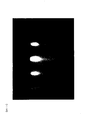
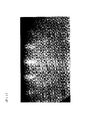
- FIG. 4 shows the reflection high-energy electron diffraction of a very thin Fe layer (an example of a ferromagnetic layer) having a thickness of 0.8 nm laminated on the surface of a “magnesium oxide (001)” layer by ultrahigh vacuum MBE at room temperature (RHEED) image.
- a spot-like diffraction pattern indicates that the Fe layer has an island-like shape.
- the thickness of the Fe layer is about 1.0 nm or less, the Fe layer becomes an island-like discontinuous film and becomes superparamagnetic instead of ferromagnetic. In this case, in order to obtain a good ferromagnetic magnetization curve with hysteresis, the thickness of the Fe layer needs to be about 1.5 nm or more.
- ferromagnetic upper electrode layer thinner than about 1 nm on a nonmagnetic layer (tunnel barrier layer) containing “magnesium oxide (001)”. It was very difficult until now.
- a multilayer film in which two or more layers having different material compositions and crystal structures are laminated is often used as the ferromagnetic layer (ferromagnetic upper electrode layer), but also in this case, It was theoretically difficult to fabricate the near-side first ferromagnetic layer (part of the ferromagnetic upper electrode layer) as a flat continuous film thinner than about 1 nm.
- the present inventors incidentally include an extremely thin certain intervening layer (3d transition metal element) on the surface of such a poorly wettable "magnesium oxide (001)" layer (tunnel barrier layer) If the oxide layer is provided, the wettability is greatly improved, and the above problems are eliminated. Moreover, even if the intervening layer is provided, the magnetoresistance ratio (MR ratio) of the TMR element is too large. It has been found that it does not deteriorate, and the present invention has been achieved.
- 3d transition metal element 3d transition metal element
- the present invention comprises many inventions related to a magnetic multilayer film and a TMR element.
- the magnetic multilayer film according to the first aspect of the present invention comprises, in order from the substrate side, a nonmagnetic layer containing single crystal or polycrystalline magnesium oxide in which the (001) crystal plane is preferentially oriented, and an extremely thin 3d transition metal element. It consists of an oxide layer and a very thin ferromagnetic layer.
- the 3d transition metal elements are the following 10 types.
- the magnetic multilayer film of the second aspect of the present invention is the magnetic multilayer film of the first aspect of the present invention, wherein the ferromagnetic layer is a first ferromagnetic layer, and the first ferromagnetic layer is thereon.
- a second ferromagnetic layer different in composition or crystal structure from the layer is added.
- the thickness of the oxide layer containing the 3d transition metal element is 0.2 to 1.5 nm. Is preferred.
- the magnetic multilayer film of the fourth aspect of the present invention is the magnetic multilayer film of any of the first to third aspects of the present invention, wherein the oxide layer containing the 3d transition metal element is Fe, Co or Ni. It is preferable to include an oxide containing at least one element.
- the magnetic multilayer film of the fifth aspect of the present invention is the magnetic multilayer film of any of the first to fourth aspects of the present invention, wherein the oxide layer containing the 3d transition metal element has a spinel structure. It is preferable to contain an oxide containing an element.
- the magnetic multilayer film of the sixth aspect of the present invention is the magnetic multilayer film of any of the first to fifth aspects of the present invention, wherein the oxide layer containing the 3d transition metal element is a spinel ferrite based 3d transition metal It is preferable to contain an oxide containing an element.
- the oxide containing the spinel ferrite-based 3d transition metal element is a compound of spinel ferrite-based ferromagnetic material or ferric It is preferable that it is a magnetic body.
- the magnetic multilayer film of the eighth aspect of the present invention is the magnetic multilayer film of any of the first to third aspects of the present invention, wherein the oxide layer containing the 3d transition metal element is maghemite, magnetite, Co ferrite or It is preferable that it is Ni ferrite.
- the magnetic multilayer film of the ninth aspect of the present invention is the magnetic multilayer film of any of the first to eighth aspects of the present invention, wherein the thickness of the ferromagnetic layer or the first ferromagnetic layer is It is preferably 0.2 to 0.8 nm.
- the magnetic multilayer film of the tenth aspect of the present invention is the magnetic multilayer film of any of the first to ninth aspects of the present invention, wherein the ferromagnetic layer or the first ferromagnetic layer is formed of “Fe It is preferable to include “a ferromagnetic metal or ferromagnetic alloy” including
- the magnetic multilayer film of the eleventh aspect of the present invention is the magnetic multilayer film of any of the first to tenth aspects of the present invention, wherein the ferromagnetic layer or the first ferromagnetic layer is formed of “Fe Or a ferromagnetic metal of a BCC structure containing Co or a ferromagnetic alloy of a BCC structure containing Fe or Co.
- a twelfth aspect of the present invention relates to a tunnel magnetoresistive element including a ferromagnetic lower electrode layer, a tunnel barrier layer and a ferromagnetic upper electrode layer in order from the substrate side.
- the element of the twelfth aspect of the present invention includes the magnetic multilayer film of any of the first to eleventh aspects of the present invention in its component, in which case the nonmagnetic layer is the tunnel barrier layer or one of them.
- the ferromagnetic layer corresponds to the ferromagnetic upper electrode layer or a part thereof, or a laminate of the first ferromagnetic layer and the second ferromagnetic layer is the ferromagnetic layer. It preferably corresponds to the upper electrode layer or a part thereof.
- the intervening layer the oxide layer containing the 3d transition metal element
- the nonmagnetic layer tunnel barrier
- the intervening layer the oxide layer containing the 3d transition metal element
- the nonmagnetic layer tunnel barrier
- the intervening layer the oxide layer containing the 3d transition metal element
- the nonmagnetic layer tunnel barrier
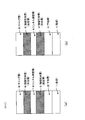
- FIG. 1A is a schematic cross-sectional view of the magnetic multilayer film and the TMR element according to the first embodiment
- FIG. 1B is a schematic cross-sectional view of the magnetic multilayer film and the TMR element according to the second embodiment
- FIG. 2 is a schematic cross-sectional view of a typical TMR element, in which (a) is an example in which a tunnel barrier layer (4) is fabricated on the fixed layer, and (b) is a tunnel barrier on the free layer. It is an example in which the layer (4) was produced.
- FIG. 3 (a) is a schematic cross-sectional view of a good tunnel barrier layer (34) formed on the lower electrode layer (31), and FIG. 3 (b) is a cross sectional view of the good tunnel barrier layer (34).
- FIG. 4 shows a 0.8 nm thick Fe layer (an example of a ferromagnetic layer) prepared at room temperature directly on a single crystal magnesium oxide layer (nonmagnetic layer, tunnel barrier layer) in which (001) crystal planes are preferentially oriented.
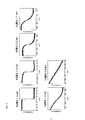
- Reflection fast electron diffraction pattern of FIG. 5 shows the magnetization curve of an Fe layer (an example of a ferromagnetic layer) having a thickness of 0.8 to 1.5 nm, which is prepared at room temperature directly on a single crystal magnesium oxide layer whose (001) crystal plane is preferentially oriented. It is the graph measured by the effect.
- FIG. 4 shows a 0.8 nm thick Fe layer (an example of a ferromagnetic layer) prepared at room temperature directly on a single crystal magnesium oxide layer (nonmagnetic layer, tunnel barrier layer) in which (001) crystal planes are preferentially oriented.
- Reflection fast electron diffraction pattern of FIG. 5 shows the magnetization curve of an Fe layer (an example of
- FIG. 6 shows a 0.3 nm thick maghemite layer (an example of an oxide layer) formed directly on a single crystal magnesium oxide layer (nonmagnetic layer, tunnel barrier layer) in which the (001) crystal plane is preferentially oriented.
- Reflection fast electron diffraction pattern of FIG. 7 shows that a 0.3 nm thick maghemite layer (oxide layer) is stacked directly on a single crystal magnesium oxide layer (nonmagnetic layer, tunnel barrier layer) in which the (001) crystal plane is preferentially oriented.
- FIG. 8 shows a 0.3 nm thick maghemite layer (oxide layer) is stacked directly on a single crystal magnesium oxide layer (nonmagnetic layer, tunnel barrier layer) in which the (001) crystal plane is preferentially oriented.
- the magnetization curve of a 0.3 to 1.5 nm thick Fe layer (ferromagnetic layer) prepared at room temperature is measured by the magneto-optical Kerr effect.
- FIG. 9 shows a 0.2 nm thick Co ferrite layer (an example of an oxide layer) formed directly on a single crystal magnesium oxide layer (nonmagnetic layer, tunnel barrier layer) in which the (001) crystal plane is preferentially oriented.
- FIG. 10 a 0.2 nm thick Co ferrite layer (oxide layer) is stacked directly on a single crystal magnesium oxide layer (nonmagnetic layer, tunnel barrier layer) in which the (001) crystal plane is preferentially oriented. It is a reflection high energy electron diffraction pattern of a 0.5 nm thick Fe layer (ferromagnetic material layer) manufactured immediately above at room temperature.
- FIG. 11 is a reflection high energy electron diffraction pattern of a 0.8 nm thick BCC Co layer formed on a 0.4 nm thick maghemite layer.
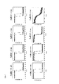
- FIG. 12 (a) is a graph of the magnetic curve of the BCC Co layer directly grown on the magnesium oxide layer measured by the magneto-optical Kerr effect
- FIG. 12 (b) is the thickness formed on the magnesium oxide layer. It is the graph which measured the magnetic curve of the BCC Co layer grown on the 0.4 nm maghemite layer by the magneto-optical Kerr effect.
- FIG. 1A is a schematic cross-sectional view of the magnetic multilayer film and the TMR element in the first embodiment.
- Reference numeral 1 is a substrate.
- Reference numeral 2 is a base layer.
- the role of the underlayer (2) is "seed layer / buffer layer" and is used to control the crystal orientation of the ferromagnetic lower electrode layer (3) stacked thereon and to improve the flatness.
- the underlayer (2) may not be necessary, and in Example 1, the ferromagnetic lower electrode layer (3) doubles as the underlayer.
- Reference numeral 4 is a nonmagnetic layer containing single crystal magnesium oxide in which the (001) crystal plane is preferentially oriented.
- Reference numeral 5 is a very thin oxide layer.
- the oxide layer (5) is disposed on the upper side of the nonmagnetic layer (4), that is, on the side far from the substrate.
- Reference numeral 6 is a very thin ferromagnetic layer (upper electrode layer).
- the ferromagnetic layer (6) is located on the oxide layer (5).
- the magnetic multilayer film of the present example is composed of the nonmagnetic layer (4), the oxide layer (5) and the ferromagnetic layer (6) in this order from the substrate (1) side.
- a ferromagnetic layer (3) which also functions as a lower electrode layer is disposed below the nonmagnetic layer (4), that is, on the substrate side.
- the ferromagnetic layer (3) corresponds to the ferromagnetic lower electrode layer
- the nonmagnetic layer (4) corresponds to the tunnel barrier layer or a part thereof
- the ferromagnetic layer (6) corresponds to the ferromagnetic upper electrode layer or a part thereof.
- the magnesium oxide constituting the nonmagnetic layer (4) may appropriately contain elements other than oxygen and magnesium.
- Example 1 maghemite (Fe 2 O 3 ) was used as the material of the oxide layer (5), and Fe was used as the material of the ferromagnetic layer (6).
- Each layer was formed using molecular beam epitaxy (MBE).
- MBE molecular beam epitaxy
- ferromagnetic lower electrode layer 3 which doubles as an underlayer (2) containing a material having a BCC (001) structure on a substrate (1) made of single crystal magnesium oxide (001)
- An Fe layer of about 100 nm thickness was formed, and a nonmagnetic layer (4) of about 2 nm thickness consisting of single crystal magnesium oxide (001) was formed thereon at room temperature.
- a multilayer film for measuring the magneto-optical Kerr effect FIGS. 6 and 8 of the ferromagnetic upper electrode layer described later, if the lower electrode layer contains a ferromagnetic material, it will interfere with the measurement.
- the Fe layer (3) was omitted, and instead a Cr layer of about 100 nm thickness having a nonmagnetic BCC (001) structure was formed as the underlayer (2). Both when the magnesium oxide (001) layer is formed on the BCC Fe (001) layer and when it is formed on BCC Cr (001), the magnesium oxide (001) layer having almost the same quality and characteristics is formed. Ru. A maghemite (Fe 2 O 3 ) layer with a thickness of 0.2 to 1.5 nm was formed as an oxide layer (5) on the nonmagnetic layer (4) made of single crystal magnesium oxide (001).
- the maghemite (Fe 2 O 3 ) layer was formed by depositing Fe at a rate of 0.005 nm / s while irradiating the substrate with atomic oxygen at a flow rate of 0.08 sccm at a substrate temperature of 130 ° C. Finally, an Fe layer of 0.2 to 2.0 nm in thickness was formed at room temperature as a ferromagnetic layer (ferromagnetic upper electrode layer 6) on the oxide layer (5).
- FIG. 6 is a reflection high energy electron diffraction (RHEED) image of a 0.3 nm thick maghemite layer formed directly on a single crystal magnesium oxide (001) layer. Since a clear streak-like RHEED pattern is obtained even at this thickness, it can be seen that a high quality maghemite layer is formed which is extremely thin, flat and has good crystallinity. In particular, it is worth noting that the maghemite layer formed directly on magnesium oxide (001), which is usually very poor in wettability, is a high quality continuous film even with a thickness of only 0.3 nm. 001) "shows that the wettability of the maghemite layer on the surface is good.
- RHEED reflection high energy electron diffraction
- Bulk maghemite has a spinel type crystal structure, and the unit cell has a lattice constant of about 0.84 nm. Therefore, when the thickness of the maghemite layer is thinner than the lattice constant of the spinel unit cell, the spinel structure can not be defined.
- the RHEED pattern (Fig. 6) of the 0.3 nm thick maghemite layer does not show the superlattice line peculiar to the spinel structure, which means that the 0.3 nm thick maghemite layer has the spinel superlattice structure. It shows that you are not.
- the RHEED pattern of a 2 nm thick maghemite layer can identify the superlattice line unique to the spinel structure, so if the thickness is 2 nm, that is, twice or more the unit cell of the spinel structure, the spinel superlattice structure It is understood that it is formed.
- the effect of the present invention can be obtained similarly with or without the superlattice structure of the spinel structure, and therefore, in the present invention, the superlattice structure of the spinel structure may be omitted. Therefore, even a maghemite layer thinner than the lattice constant of the spinel unit cell can be positively used in the oxide layer.
- spinel is included, including the case where there is no superlattice structure of spinel structure. We call it "structure”.
- FIG. 7 is a RHEED image of a 0.8 nm thick Fe layer formed on a 0.3 nm thick maghemite layer.
- the RHEED image of FIG. 7 is a clear streak-like pattern and is flat even if it is thinner than 1 nm It shows that a high quality Fe layer was formed. That is, it was shown that the Fe layer on the surface of the maghemite layer has very good wettability. Thus, it was found that the wettability of the Fe layer is greatly improved by inserting an extremely thin maghemite layer between the magnesium oxide (001) layer and the Fe layer.
- FIG. 8 shows a measurement of the magnetization curve at room temperature of a 0.3 to 1.5 nm thick Fe layer formed on a 0.3 nm thick maghemite layer by the magneto-optical Kerr effect.
- FIG. 8 shows a good ferromagnetic magnetization curve even with an Fe layer having a thickness of only 0.4 nm. Furthermore, even at a thickness of 0.3 nm, a ferromagnetic tendency appears. From the results of the magnetization measurement, it was revealed that the Fe layer formed on the maghemite layer is a flat continuous film with a thickness of 0.2 nm or more.
- the extremely thin oxide layer 5 (maghemite layer) is inserted between the nonmagnetic layer (4) containing "magnesium oxide (001)" and the ferromagnetic layer 6 (Fe layer).
- the wettability of the ferromagnetic layer (6) to the nonmagnetic layer (4) is significantly improved, as a result of which a flat and high quality continuous film of very thin but even on the nonmagnetic layer (4) It became possible to form a ferromagnetic layer (6).
- This discovery reverses the conventional wisdom of crystal growth that a very thin and flat ferromagnetic layer can not be fabricated on a very poorly wettable "magnesium oxide (001)" layer.
- the physical mechanism and principle of crystal growth in the present invention are still unknown.
- the magnetic multilayer film of the present invention When the magnetic multilayer film of the present invention is used as a component of a TMR element, it is also an important requirement to obtain a large MR ratio at room temperature. Basically, if the oxide layer (5) is inserted between the nonmagnetic layer (4) and the ferromagnetic layer (6), the MR ratio decreases, but if the oxide layer (5) is thin, the MR will Since the reduction of the ratio is limited, it is not particularly problematic. However, when the oxide layer (5) becomes thinner than 0.2 nm, the average thickness becomes thinner than one atomic layer, so in fact a part of the surface of the nonmagnetic layer (4) is covered with the oxide layer (5) In some cases, the effect of improving wettability can not be obtained.
- the thickness of the oxide layer (5) is preferably 0.2 to 1.5 nm, more preferably 0.2 to 1.0 nm, still more preferably 0.2 to 0.8 nm, 0.2 to 0.6 nm or 0.2 to 0.4 nm. good.
- the oxide layer (5) should be thin from the viewpoint of the MR ratio, but the oxide layer (5) can be optimized by considering the effect of wettability improvement and the value of the optimal RA product, etc. The thickness is determined. In fact, the optimum thickness of the oxide layer (5) is appropriately set in accordance with various characteristics such as the magnetoresistance ratio and the RA value required for various applications.
- maghemite is used as the material of the oxide layer (5) in Example 1, the effect of wettability improvement can be obtained even with oxides containing various other 3d transition metal elements.
- using an oxide containing at least one element of Fe, Co and Ni is effective for improving the wettability of the surface of the "magnesium oxide (001)" layer.
- an oxide containing a 3d transition metal element having a spinel structure is particularly effective for improving the wettability of the surface of the "magnesium oxide (001)” layer because it has a good lattice matching with the "magnesium oxide (001)" layer. It is.
- FIG. 9 shows a reflection high energy electron diffraction (RHEED) image of a 0.2 nm thick Co ferrite layer formed directly on single crystal magnesium oxide (001).
- RHEED reflection high energy electron diffraction
- the magnetic multilayer film of the present invention when used as a component of a TMR element, it is also an important effect that a large MR ratio can be obtained at room temperature as described above.
- an oxide containing a spinel ferrite-based 3d transition metal element as the material of the oxide layer (5), the reduction of the MR ratio can be suppressed as compared with the case where the oxide layer (5) is not provided.
- the oxide layer (5) is a "ferromagnetic or ferrimagnetic spinel ferrite material"
- a larger magnetoresistance effect can be obtained due to the spin filter effect caused by the spin-polarized insulator band structure.
- maghemite was used as an example of “ferromagnetic or ferrimagnetic spinel ferrite material”. In this case, a large MR ratio of about 100% was obtained at room temperature in a thickness range of 0.2 to 1.0 nm.
- materials such as magnetite, Co ferrite, and Ni ferrite can be used besides maghemite.
- Co ferrite and Ni ferrite are preferable to maghemite as the material of the oxide layer (5) because they have a very high Curie temperature and a large spin filter effect.
- magnetite has a half metal band structure and is an effective material for obtaining a larger MR ratio and a lower RA product.
- a spinel ferrite-based oxide containing at least one element of Fe, Co, Ni, etc. and oxygen, and optionally adding other elements is suitable as a material of the oxide layer (5)
- the composition may be set appropriately according to various characteristics such as MR ratio and RA value required for various applications. Note that, as described above, the thickness of the spinel ferrite-based oxide layer may be thinner than the lattice constant of the spinel unit cell and may not have the spinel superlattice structure.
- the material of the ferromagnetic layer 6 is preferably a 3d transition metal element or an alloy thereof.
- a ferromagnetic metal or Fe containing Fe as a material of the ferromagnetic layer 6 (upper electrode layer) in order to obtain a large MR ratio at room temperature
- an alloy more preferably a ferromagnetic metal or ferromagnetic alloy of a BCC structure containing Fe.
- the optimum thickness of the ferromagnetic layer 6 (upper electrode layer) may be appropriately set in accordance with various properties necessary for various applications. From the viewpoint of reducing power consumption in applications such as a spin torque type MRAM and a high frequency oscillator, it is better for the ferromagnetic layer 6 (upper electrode layer) to be thinner.
- the thickness of the ferromagnetic layer 6 (upper electrode layer) may be 0.8 nm or less, more preferably 0.6 nm or less, and still more preferably 0.4 nm or less.
- the thickness of the ferromagnetic layer 6 (upper electrode layer) is less than 0.2 nm, the ferromagnetic layer 6 (upper electrode layer) may not completely cover the surface of the oxide layer (5). Therefore, the ferromagnetic layer 6 (upper electrode layer) needs to have a thickness of at least about 0.2 nm.
- the thickness of the ferromagnetic layer 6 (upper electrode layer) should be 0.3 nm or more, more preferably 0.4 nm or more. The thickness of the ferromagnetic layer 6 (upper electrode layer) depends on whether low power consumption is prioritized, stable ferromagnetism at room temperature is prioritized, or a large MR ratio is prioritized in various applications. Should be set appropriately.
- Example 1 Although the MBE method is used as the film forming method in the first embodiment, other physical film forming methods (PVD) such as sputtering method or chemical film forming method (CVD) can be used. Further, in Example 1, atomic oxygen was used as an oxygen source at the time of film formation of the oxide layer (5). As another method, (i) an oxide containing a 3d transition metal element in the material of the evaporation source (Ii) using a material containing a 3d transition metal as the material of the vapor deposition source and using an oxidizing source such as molecular oxygen, radical oxygen, plasma oxygen, ozone, and the like.
- PVD physical film forming methods
- CVD chemical film forming method
- Example 1 single-crystal magnesium oxide (001) was used as the nonmagnetic layer (4), but even if polycrystal magnesium oxide in which the (001) crystal plane is preferentially oriented is used in principle, the same invention An effect is obtained. From the viewpoint of production cost, polycrystalline is more preferable than single crystal.
- Example 1 single crystal magnesium oxide (001) was used as a substrate, but the substrate may be basically anything. By laminating various underlayers on an arbitrary substrate, it is possible to produce a nonmagnetic layer (4) containing single crystal or polycrystalline magnesium oxide in which the (001) crystal plane is preferentially oriented. It is possible.
- FIG. 1B is a schematic cross-sectional view of the magnetic multilayer film and the TMR element in the second embodiment.
- the difference from Example 1 is that the ferromagnetic layer (6) of Example 1 is the first ferromagnetic layer (6) and the second ferromagnetic layer (Example 2).
- the first embodiment and the second embodiment are exactly the same as the seventh embodiment except that 7) is replaced.
- the very thin first ferromagnetic layer (6) is disposed on the very thin oxide layer (4), and the second ferromagnetic layer (7) is disposed thereon. If necessary, further different ferromagnetic layers may be disposed on the second ferromagnetic layer (7).
- an extremely thin nonmagnetic layer such as Ru, Ta, Cu, or MgO may be inserted between the first ferromagnetic layer (6) and the second ferromagnetic layer (7). Good.
- an extremely thin nonmagnetic layer such as Ru, Ta, Cu, or MgO may be inserted between the first ferromagnetic layer (6) and the second ferromagnetic layer (7). Good.
- the magnetic multilayer film of the present invention when used as a component of a TMR element, a material exhibiting a high MR ratio in the first ferromagnetic layer (6), a desired magnetic property in the second ferromagnetic layer (7) If a material exhibiting properties is used to cause the two layers to effectively act as a single ferromagnetic layer (upper electrode layer) by the exchange coupling acting at the interface of these two layers, a high MR ratio and a desired magnetic property can be obtained. It becomes possible to realize the characteristics simultaneously.
- the material of the first ferromagnetic layer (6) is preferably a 3d transition metal element or an alloy thereof.
- a ferromagnetic metal or Fe containing Fe as a material of the first ferromagnetic layer (6) is used to obtain a large MR ratio at room temperature. It is preferable to use a magnetic alloy, more preferably a ferromagnetic metal or ferromagnetic alloy having a BCC structure containing Fe.
- the optimum thickness of the first ferromagnetic layer (6) is appropriately set in accordance with the various properties required for various applications. From the viewpoint of reducing power consumption in applications such as spin torque MRAM and high frequency oscillator, it is better for the first ferromagnetic layer (6) to be thinner.
- the thickness of the first ferromagnetic layer (6) is preferably in the range of 0.8 nm or less, more preferably 0.6 nm or less, and still more preferably 0.4 nm or less.
- the first ferromagnetic layer (6) may not completely cover the surface of the oxide layer (5).
- the first ferromagnetic layer (6) needs to have a thickness of at least 0.2 nm. Furthermore, in order to obtain stable ferromagnetism at room temperature, the thickness of the first ferromagnetic layer (6) is preferably 0.3 nm or more, more preferably 0.4 nm or more. The thickness of the first ferromagnetic layer (6) depends on whether low power consumption is preferred, stable ferromagnetism at room temperature is prioritized, or a large MR ratio is prioritized in various applications. Needs to be set appropriately.
- a soft magnetic material such as permalloy is used as the second ferromagnetic layer (7)
- a laminate of the first ferromagnetic layer (6) and the second ferromagnetic layer (6) is used.
- Soft magnetic properties can be imparted.
- the magnetic multilayer film of the second embodiment is used as a component of a TMR element, soft magnetic characteristics can be imparted to the ferromagnetic upper electrode layer, and a device which operates with a smaller applied magnetic field or spin torque can be obtained. realizable.
- a perpendicular magnetization material or a perpendicular magnetic anisotropy material is used as the second ferromagnetic layer (7)
- a laminate of the first ferromagnetic layer (6) and the second ferromagnetic layer (7) is used.
- Perpendicular magnetic properties can be imparted to the material.
- the magnetic multilayer film of Example 2 is used as a component of a TMR element
- perpendicular magnetic characteristics can be imparted to the ferromagnetic upper electrode layer, and it can be used for a highly integrated spin torque MRAM. .
- an alloy of L1 0 ordered structure such as Mn-Ga, ferromagnetic metal or alloy thereof and a non-magnetic metal Or a multilayer film obtained by laminating the alloy
- an alloy of a 3d transition metal element such as Tb-Co or Tb-Fe-Co and a rare earth metal
- a metal of HCP structure containing Co or its alloy a metal of HCP structure containing Co or its alloy
- the first ferromagnetic layer By inserting a nonmagnetic layer such as ruthenium (Ru) of appropriate thickness between the first ferromagnetic layer (6) and the second ferromagnetic layer (7), the first ferromagnetic layer It is possible to orient the magnetization of the body layer (6) and the magnetization of the second ferromagnetic layer (7) antiparallel. Thereby, it is possible to reduce the leakage magnetic field from the laminate of the first ferromagnetic layer (6) and the second ferromagnetic layer (7).
- ruthenium ruthenium
- a nonmagnetic layer is inserted between the first ferromagnetic layer (6) and the second ferromagnetic layer (7) to divide the exchange coupling between the two layers, and further, the first ferromagnetic layer
- the magnetization and the second strong of the first ferromagnetic layer (6) The relative angle of magnetization of the magnetic layer (7) can be about 90 °. This makes it possible to reduce the operating current density in applications such as high frequency oscillators.
- Example 3 In Example 1, Fe was used as the material of the ferromagnetic layer (6), but Co was used here.
- the BCC Co layer which is a metastable crystal layer, is difficult to grow and form on a nonmagnetic layer (4) such as magnesium oxide.
- an oxide layer (5) consisting of a very thin 0.4 nm thick maghemite layer is previously formed on the nonmagnetic layer (4), and a very thin BCC Co of about 0.8 nm thick is formed thereon.
- a magnetic multilayer film was produced by forming a ferromagnetic layer (6) composed of layers.
- FIG. 1 A comparison of the magnetic properties with the case of direct growth and film formation on the magnesium oxide layer, ie, the nonmagnetic layer (4) is shown in FIG.
- the thickness of the BCC Co layer is 0.8, reflecting the magnetocrystalline anisotropy of the epitaxially grown BCC Co (001) layer. It has been found that a hysteresis excellent in squareness is obtained even in the case of an ultra-thin film of nm, and that the ferromagnetism is maintained even when the thickness of the BCC Co layer is 0.6 nm.
- the BCC Co layer is known to exhibit higher magnetoresistance properties than the Fe layer, and according to the invention, the ferromagnetic layer (6) consisting of a very thin BCC Co layer on the nonmagnetic layer (4) The formation process is very effective in improving the characteristics of the TMR element.
Landscapes
- Hall/Mr Elements (AREA)
- Thin Magnetic Films (AREA)
- Mram Or Spin Memory Techniques (AREA)
Description
スピントルク型MRAMは、トンネル磁気抵抗素子(TMR素子;Tunnel Magneto-Resistance Element、あるいは磁気トンネル接合素子(MTJ素子)とも呼ばれる)を単位記憶素子として、そこに電流を流すことで強磁性体層の磁化の方向が反転するスピントルク磁化反転と呼ばれる現象を利用した記憶素子である。TMR素子は、簡単に言えば、トンネル障壁層を2つの強磁性体層(2つの強磁性体層の一方を「強磁性下部電極層」、他方を「強磁性上部電極層」と呼ぶこともある)で挟んだ構造を持っている。1つの強磁性体層からトンネル障壁層を介して他の強磁性体層に向かって電流を流した際に、2つの強磁性体層の磁化の方向が平行(パラレル)になったり反平行(アンチパラレル)になったりすることで、TMR素子が低抵抗になったり高抵抗になるトンネル磁気抵抗効果(TMR効果)という現象を、デジタル情報の“1”と“0”に対応させることで、TMR素子が不揮発性の磁気メモリとして利用される。
研究開発の当初は、強磁性層の磁化が膜面内方向に向いた面内磁化であったが、最近ではより高密度化を狙って膜面垂直方向に磁化が向いた垂直磁化を用いたMRAMも開発されつつある。
(理由1) 素子の用途により、1.スピントルク磁化反転を誘起するのに必要な電流密度、又は2.高周波発振を誘起するのに必要な電流密度は、自由層が薄いほど低くなる。電流密度の低減は消費電力の低減や高密度化につながり、さらに素子の長期信頼性の向上にも有効なので、基本的に電流密度は低いほど良い。
(理由2) 自由層が薄いほど自由層と固定層の間に働く静磁気結合を下げることができる。一般に、この静磁気結合が大きいとMRAMにおいて零磁界付近で2値安定状態を保てなくなるなどの問題が生じるため、素子の動作が不安定になりやすい。さらに、MRAMなどのメモリに利用する場合、多数のTMR素子を1つの基板上にマトリックス上に配置するが、一つの素子の自由層から隣の素子の自由層への漏洩磁界がある。漏洩磁界が大きいと隣の素子の情報書き換えが不安定になるなど、様々な問題が生じる。自由層が薄いほど、この漏洩磁界が小さくなるので応用上好ましい。
(i)トンネル障壁層の基板側に固定層(強磁性体層)を配置し、基板と反対側に自由層(強磁性体層)を配置する構造(図2(a)参照)、
(ii)トンネル障壁層の基板側に自由層(強磁性体層)を配置し、基板と反対側に固定層(強磁性体層)を配置する構造(図2(b) 参照)、
の2種類がある。このうち、(i)の構造は、素子加工が容易、固定層の信頼性が上がる、などの利点を有しているため、磁気センサー応用では(i)の構造が用いられることが多い。一方、スピントルク型MRAMや高周波発振素子などの応用においては、(i)の構造は後述のように自由層を薄くできないという欠点を有する。一方、(ii)の構造では自由層を薄くできるが、固定層を薄くできない、固定層の信頼性が低下しやすい、などの欠点がある。
図5は、“酸化マグネシウム(001)”層の表面上にMBE法により室温で積層したFe層(強磁性体層)の室温における磁化曲線を磁気光学Kerr効果により測定したものである。Fe層の厚さが約1.0nm以下のとき、Fe層が島状の不連続膜となり、強磁性ではなく超常磁性的になってしまう。この場合、ヒステリシスを持つ良好な強磁性的磁化曲線を得るには、Fe層の厚さが約1.5nm以上である必要がある。
本発明の第1の態様の磁気多層膜は、基板側から順に、(001)結晶面が優先配向した単結晶又は多結晶の酸化マグネシウムを含む非磁性体層、極めて薄い3d遷移金属元素を含む酸化物層、及び極めて薄い強磁性体層からなる。
3d遷移金属元素とは、次の10種である。Sc(スカンジウム)、Ti(チタン)、V(バナジウム)、Cr(クロム)、Mn(マンガン)、Fe(鉄)、Co(コバルト)、Ni(ニッケル)、Cu(銅)、Zn(亜鉛)
もちろん、これらの元素は前記酸化物に複数混合されていても良い(例えばCoフェライト)。また、本発明の本質を損なわない限り、第三の元素が単独で又は複数で混合されて前記酸化物となっていても良いし、あるいは前記酸化物に第三物質が混合されていても良い。
本発明の第2の態様の磁気多層膜は、本発明の第1の態様の磁気多層膜において、前記強磁性体層を第1の強磁性体層とし、その上に第1の強磁性体層とは組成あるいは結晶構造の異なる第2の強磁性体層が付加されていることが好ましい。
本発明の第3の態様の磁気多層膜は、本発明の第1又は第2の態様の磁気多層膜において、前記3d遷移金属元素を含む酸化物層の膜厚が0.2~1.5nmであることが好ましい。
本発明の第4の態様の磁気多層膜は、本発明の第1~第3のいずれかの態様の磁気多層膜において、前記3d遷移金属元素を含む酸化物層がFe、Co、Niのうち少なくとも1元素を含む酸化物を含むことが好ましい。
本発明の第5の態様の磁気多層膜は、本発明の第1~第4のいずれかの態様の磁気多層膜において、前記3d遷移金属元素を含む酸化物層がスピネル構造を持つ3d遷移金属元素を含む酸化物を含むことが好ましい。
本発明の第6の態様の磁気多層膜は、本発明の第1~第5のいずれかの態様の磁気多層膜において、前記3d遷移金属元素を含む酸化物層がスピネルフェライト系の3d遷移金属元素を含む酸化物を含むことが好ましい。
本発明の第7の態様の磁気多層膜は、本発明の第6の態様の磁気多層膜において、前記スピネルフェライト系の3d遷移金属元素を含む酸化物が「スピネルフェライト系の強磁性体またはフェリ磁性体」であることが好ましい。
本発明の第8の態様の磁気多層膜は、本発明の第1~第3のいずれかの態様の磁気多層膜において、前記3d遷移金属元素を含む酸化物層がマグヘマイト、マグネタイト、Coフェライト又はNiフェライトであることが好ましい。
本発明の第9の態様の磁気多層膜は、本発明の第1~第8のいずれかの態様の磁気多層膜において、前記強磁性体層又は前記第1の強磁性体層の膜厚が0.2~0.8nmであることが好ましい。
本発明の第10の態様の磁気多層膜は、本発明の第1~第9のいずれかの態様の磁気多層膜において、前記強磁性体層又は前記第1の強磁性体層は、「Feを含む強磁性金属又は強磁性合金」を含むことが好ましい。
本発明の第11の態様の磁気多層膜は、本発明の第1~第10のいずれかの態様の磁気多層膜において、前記強磁性体層又は前記第1の強磁性体層は、「FeもしくはCoを含むBCC構造の強磁性金属又はFeもしくはCoを含むBCC構造の強磁性合金」を含むことが好ましい。
本発明の第12の態様は、基板側から順に強磁性下部電極層、トンネル障壁層及び強磁性上部電極層を含むトンネル磁気抵抗素子に関する。本発明の第12の態様の素子は、その構成要素に本発明の第1~11のいずれかの態様の磁気多層膜を含み、その場合、前記非磁性体層が前記トンネル障壁層またはその一部に相当し、前記強磁性体層が前記強磁性上部電極層又はその一部に相当し、或いは前記1の強磁性体層と前記第2の強磁性体層との積層物が前記強磁性上部電極層又はその一部に相当することが好ましい。
なお、説明の簡単のためにこれ以下「3d遷移金属元素を含む酸化物層」を単に「酸化物層」と略称すことがある。)
<実施例1>
図1の(a)に本実施例1における磁気多層膜及びTMR素子の断面模式図を示す。符号1は基板である。符号2は下地層である。下地層(2)の役目は「シード層/バッファ層」であり、その上に積層する強磁性下部電極層(3)の結晶配向性の制御や平坦性の向上のために用いる。下地層(2)が必要ない場合もあり、実施例1では、強磁性下部電極層(3)が下地層を兼ねている。符号4は、(001)結晶面が優先配向した単結晶酸化マグネシウムを含む非磁性体層である。符号5は極めて薄い酸化物層である。酸化物層(5)は非磁性層(4)の上側つまり基板から遠い側に配置されている。符号6は極めて薄い強磁性体層(上部電極層)である。強磁性体層(6)は酸化物層(5)の上に位置する。
このように本実施例の磁気多層膜は、基板(1)側から順に非磁性体層(4)、酸化物層(5)及び強磁性体層(6)から構成される。
また、非磁性体層(4)の下側、つまり基板側には下部電極層としても作用する強磁性体層(3)を配置する。
この磁気多層膜をトンネル磁気抵抗素子の構成要素として用いる場合、強磁性体層(3)が強磁性下部電極層に相当し、非磁性体層(4)がトンネル障壁層またはその一部に相当し、強磁性体層(6)が強磁性上部電極層又はその一部に相当する。なお、非磁性体層(4)を構成する酸化マグネシウムには、酸素とマグネシウム以外の元素が適宜含まれていてもよい。
各層は、分子線エピタキシー法(MBE法)を用いて形成した。MBE法では、最高到達真空度が約2×10⁻⁸Paの超高真空MBE成膜装置を用いた。
まず、単結晶の酸化マグネシウム(001)から成る基板(1)の上にBCC(001)構造を持つ材料を含む下地層(2)を兼ねた強磁性体層(強磁性下部電極層3)として厚さ約100nmのFe層を形成し、その上に単結晶の酸化マグネシウム(001)から成る厚さ約2nmの非磁性層(4)を室温で形成した。なお、後述する強磁性上部電極層の磁気光学Kerr効果(図6と図8)を測定するための多層膜では、下部電極層に強磁性材料が含まれていると測定上の邪魔になるため、Fe層(3)を省き、その代わり下地層(2)として非磁性でBCC(001)構造を持つ厚さ約100nmのCr層を形成した。
酸化マグネシウム(001)層をBCC Fe(001)層の上に作製した場合も、BCCCr(001)の上に作製した場合も、ほぼ同一の品質と特性を持つ酸化マグネシウム(001)層が形成される。
単結晶の酸化マグネシウム(001)から成る非磁性層(4)の上に、酸化物層(5)として、厚さ0.2~1.5nmのマグヘマイト(Fe2O3)層を形成した。マグヘマイト(Fe2O3)層は、基板温度130℃において、流量0.08sccmの原子状酸素を基板に照射しながらFeを0.005nm/sのレートで蒸着することにより形成した。最後に酸化物層(5)の上に強磁性体層(強磁性上部電極層6)として、厚さ0.2~2.0nmのFe層を室温で形成した。
一方、厚さ2nmのマグヘマイト層のRHEEDパターンではスピネル構造特有の超格子線が確認できるため、厚さ2nm、つまりスピネル構造のユニットセルの2倍以上の厚さになるとスピネル構造の超格子構造が形成されることが分かる。このようにスピネル構造の超格子構造がある場合でも無い場合でも本発明の効果が同様に得られるため、本発明においてはスピネル構造の超格子構造は無くても構わない。したがって、スピネル構造のユニットセルの格子定数よりも薄いマグヘマイト層でも、酸化物層に積極的に用いることができる。なお、上述のようにスピネル構造のユニットセルの格子定数よりも薄い酸化物層の結晶構造を表す一般名称が存在しないため、本発明においてはスピネル構造の超格子構造が無い場合も含めて「スピネル構造」と呼ぶこととする。
以上をまとめると、“酸化マグネシウム(001)”を含む非磁性体層(4)と強磁性体層6(Fe層)との間に極めて薄い酸化物層5(マグヘマイト層)を挿入することによって、非磁性体層(4)に対する強磁性体層(6)の濡れ性が大幅に改善され、その結果、非磁性体層(4)上に非常に薄くても平坦で高品質な連続膜の強磁性体層(6)を形成することが可能となった。この発見は、極めて濡れ性の悪い“酸化マグネシウム(001)”層の上には非常に薄くて平坦な強磁性体層は作製できない、という従来の結晶成長の常識を覆すものである。ただし、本発明における結晶成長の物理的な機構や原理は、未だ不明である。
「強磁性またはフェリ磁性のスピネルフェライト系材料」としてマグヘマイト以外にも、マグネタイト、Coフェライト、Niフェライトなどの材料がある。CoフェライトやNiフェライトは、非常に高いキュリー温度や大きなスピンフィルター効果を有しているため、酸化物層(5)の材料としてマグヘマイトよりも好ましい。また、マグネタイトはハーフメタルのバンド構造を持っているため、より大きなMR比と低いRA積を得るために有効な材料である。基本的に、Fe、Co、Niなどのうち少なくとも1元素と酸素を含み、さらに必要に応じて他の元素を添加したスピネルフェライト系の酸化物が、酸化物層(5)の材料として適しており、その組成は各種応用のために必要なMR比やRA値などの諸特性に応じて適宜設定するとよい。なお、前述の通り、スピネルフェライト系の酸化物層の厚さがスピネル構造のユニットセルの格子定数よりも薄くて、スピネル構造の超格子構造を有していなくても構わない。
図1(b)に、実施例2における磁気多層膜及びTMR素子の断面模式図を示す。実施例1(図1(a))との違いは、実施例1の強磁性体層(6)が実施例2では第1の強磁性体層(6)と第2の強磁性体層(7)に置き換わっただけであり、この他の構成要素に関しては実施例1と実施例2は全く同じである。極めて薄い酸化物層(4)の上に、極めて薄い第1の強磁性体層(6)を配置し、さらにその上に第2の強磁性体層(7)を配置する。必要に応じて、第2の強磁性体層(7)の上に、さらに異なる強磁性体層を配置してもよい。さらに、必要に応じて、第1の強磁性体層(6)と第2の強磁性体層(7)の間にRuやTa、Cu、MgOなどの極めて薄い非磁性層を挿入してもよい。図1(b)のように、2層以上の強磁性体層を積層することによって、各種応用に応じた磁気特性やMR比の最適化が可能となる。例えば、本発明の磁気多層膜をTMR素子の構成要素として用いる場合、第1の強磁性体層(6)に高いMR比を示す材料、第2の強磁性体層(7)に所望の磁気特性を示す材料を用い、これら2層の界面に働く交換結合により、これら2層が事実上1層の強磁性体層(上部電極層)として振る舞うようにすれば、高いMR比と所望の磁気特性を同時に実現することが可能となる。
実施例1では強磁性体層(6)の材料としてFeを用いたが、ここではCoを用いた。従来、準安定結晶層であるBCC Co層は、酸化マグネシウムのような非磁性体層(4)の上には成長、成膜が困難である。ここでは、非磁性体層(4)の上に予め極めて薄い厚さ0.4nmのマグヘマイト層からなる酸化物層(5)を形成しておき、その上に極めて薄い厚さ0.8nm程度のBCC Co層からなる強磁性体層(6)を形成することにより磁気多層膜を作製した。
日本国出願2012年第192115号(2012年8月31日)
2…下地層、
3…下部の強磁性体層(強磁性下部電極層)、
4…非磁性体層(トンネル障壁層又はその一部)、
5…3d遷移金属元素を含む酸化物層、
6…上部の強磁性体層又は第1の強磁性層(強磁性上部電極層又はその一部)、
7…第2の強磁性体層(強磁性上部電極層又はその一部)、
8…キャップ層、
33…下部電極層、
34…非磁性体層(トンネル障壁層又はその一部)、
36…強磁性体層又は第1の強磁性体層
Claims (12)
- 基板側から順に、(001)結晶面が優先配向した単結晶又は多結晶の酸化マグネシウムを含む非磁性体層、極めて薄い3d遷移金属元素を含む酸化物層及び極めて薄い強磁性体層からなる磁気多層膜。
- 請求項1に記載の磁気多層膜において、前記強磁性体層を第1の強磁性体層とし、その上に第1の強磁性体層とは組成あるいは結晶構造の異なる第2の強磁性体層を付加した磁気多層膜。
- 請求項1又は2に記載の磁気多層膜において、前記3d遷移金属元素を含む酸化物層の膜厚が0.2~1.5nmである磁気多層膜。
- 請求項1~3のいずれかに記載の磁気多層膜において、前記3d遷移金属元素を含む酸化物層がFe、Co、Niのうち少なくとも1元素を含む酸化物を含む磁気多層膜。
- 請求項1~4のいずれかに記載の磁気多層膜において、前記3d遷移金属元素を含む酸化物層が“スピネル構造を持つ3d遷移金属元素を含む酸化物”を含む磁気多層膜。
- 請求項1~5のいずれかに記載の磁気多層膜において、前記3d遷移金属元素を含む酸化物層が“スピネルフェライト系の3d遷移金属元素を含む酸化物”を含む磁気多層膜。
- 請求項6に記載の磁気多層膜において、前記“スピネルフェライト系の3d遷移金属元素を含む酸化物”が強磁性またはフェリ磁性のスピネルフェライト系材料である磁気多層膜。
- 請求項1~3のいずれかに記載の磁気多層膜において、前記3d遷移金属元素を含む酸化物層がマグヘマイト、マグネタイト、Coフェライト又はNiフェライトを含む磁気多層膜。
- 請求項1~8のいずれかに記載の磁気多層膜において、前記強磁性体層又は前記第1の強磁性体層の膜厚が0.2~0.8?nmである磁気多層膜。
- 請求項1~9のいずれかに記載の磁気多層膜において、前記強磁性体層又は前記第1の強磁性体層は、Feを含む強磁性金属又はFeを含む強磁性合金を含む磁気多層膜。
- 請求項1~10のいずれかに記載の磁気多層膜において、前記強磁性体層又は前記第1の強磁性体層は、FeもしくはCoを含むBCC構造の強磁性金属又はFeもしくはCoを含むBCC構造の強磁性合金を含む磁気多層膜。
- 基板側から順に強磁性下部電極層、トンネル障壁層及び強磁性上部電極層を含むトンネル磁気抵抗素子であって、
その構成要素に請求項1~11のいずれかに記載の磁気多層膜を含み、
その場合、前記非磁性体層が前記トンネル障壁層またはその一部に相当し、前記強磁性体層が前記強磁性上部電極層又はその一部に相当し、或いは前記1の強磁性体層と前記第2の強磁性体層との積層物が前記強磁性上部電極層又はその一部に相当するトンネル磁気抵抗素子。
Priority Applications (2)
| Application Number | Priority Date | Filing Date | Title |
|---|---|---|---|
| JP2014533009A JP6049032B2 (ja) | 2012-08-31 | 2013-08-27 | 磁気多層膜及びトンネル磁気抵抗素子 |
| US14/423,978 US20150280111A1 (en) | 2012-08-31 | 2013-08-27 | Magnetic multilayer film and tunneling magnetoresistance element |
Applications Claiming Priority (2)
| Application Number | Priority Date | Filing Date | Title |
|---|---|---|---|
| JP2012-192115 | 2012-08-31 | ||
| JP2012192115 | 2012-08-31 |
Publications (1)
| Publication Number | Publication Date |
|---|---|
| WO2014034639A1 true WO2014034639A1 (ja) | 2014-03-06 |
Family
ID=50183451
Family Applications (1)
| Application Number | Title | Priority Date | Filing Date |
|---|---|---|---|
| PCT/JP2013/072812 Ceased WO2014034639A1 (ja) | 2012-08-31 | 2013-08-27 | 磁気多層膜及びトンネル磁気抵抗素子 |
Country Status (3)
| Country | Link |
|---|---|
| US (1) | US20150280111A1 (ja) |
| JP (1) | JP6049032B2 (ja) |
| WO (1) | WO2014034639A1 (ja) |
Cited By (1)
| Publication number | Priority date | Publication date | Assignee | Title |
|---|---|---|---|---|
| JP2016063085A (ja) * | 2014-09-18 | 2016-04-25 | 三星電子株式会社Samsung Electronics Co.,Ltd. | 磁気トンネル接合素子及び磁気ランダムアクセスメモリ |
Families Citing this family (3)
| Publication number | Priority date | Publication date | Assignee | Title |
|---|---|---|---|---|
| KR102276541B1 (ko) * | 2014-11-27 | 2021-07-13 | 삼성전자주식회사 | 자기 메모리 장치 및 이의 제조 방법 |
| JP2019047119A (ja) * | 2017-09-04 | 2019-03-22 | Tdk株式会社 | 磁気抵抗効果素子、磁気メモリ、および磁気デバイス |
| KR20220125050A (ko) | 2021-03-04 | 2022-09-14 | 삼성전자주식회사 | 자기터널접합 소자, 자기터널접합 소자를 포함하는 메모리 장치, 및 자기터널접합 소자의 제조 방법 |
Citations (4)
| Publication number | Priority date | Publication date | Assignee | Title |
|---|---|---|---|---|
| WO2006022183A1 (ja) * | 2004-08-27 | 2006-03-02 | Japan Science And Technology Agency | 磁気抵抗素子及びその製造方法 |
| JP2007150265A (ja) * | 2005-10-28 | 2007-06-14 | Toshiba Corp | 磁気抵抗効果素子および磁気記憶装置 |
| JP2008034523A (ja) * | 2006-07-27 | 2008-02-14 | National Institute Of Advanced Industrial & Technology | Cpp型巨大磁気抵抗素子および磁気センサ |
| JP2008085170A (ja) * | 2006-09-28 | 2008-04-10 | Toshiba Corp | 磁気抵抗効果型素子および磁気抵抗効果型ランダムアクセスメモリ |
Family Cites Families (6)
| Publication number | Priority date | Publication date | Assignee | Title |
|---|---|---|---|---|
| JP2003332127A (ja) * | 2002-05-13 | 2003-11-21 | National Institute Of Advanced Industrial & Technology | 軟磁性フェライト材料の製造方法 |
| US7576956B2 (en) * | 2004-07-26 | 2009-08-18 | Grandis Inc. | Magnetic tunnel junction having diffusion stop layer |
| US20070096229A1 (en) * | 2005-10-28 | 2007-05-03 | Masatoshi Yoshikawa | Magnetoresistive element and magnetic memory device |
| JP4998994B2 (ja) * | 2007-05-22 | 2012-08-15 | 国立大学法人 筑波大学 | 反強磁性的層間結合磁性膜を用いた磁気記録媒体及び磁気記憶装置 |
| JP5576643B2 (ja) * | 2009-12-10 | 2014-08-20 | エイチジーエスティーネザーランドビーブイ | トンネル接合型磁気抵抗効果素子、トンネル接合型磁気抵抗効果ヘッド、磁気記録再生装置、及びその製造方法 |
| JP5356431B2 (ja) * | 2011-02-17 | 2013-12-04 | 株式会社東芝 | 磁気抵抗効果素子、磁気ヘッドアセンブリ及び磁気記録装置 |
-
2013
- 2013-08-27 JP JP2014533009A patent/JP6049032B2/ja active Active
- 2013-08-27 WO PCT/JP2013/072812 patent/WO2014034639A1/ja not_active Ceased
- 2013-08-27 US US14/423,978 patent/US20150280111A1/en not_active Abandoned
Patent Citations (4)
| Publication number | Priority date | Publication date | Assignee | Title |
|---|---|---|---|---|
| WO2006022183A1 (ja) * | 2004-08-27 | 2006-03-02 | Japan Science And Technology Agency | 磁気抵抗素子及びその製造方法 |
| JP2007150265A (ja) * | 2005-10-28 | 2007-06-14 | Toshiba Corp | 磁気抵抗効果素子および磁気記憶装置 |
| JP2008034523A (ja) * | 2006-07-27 | 2008-02-14 | National Institute Of Advanced Industrial & Technology | Cpp型巨大磁気抵抗素子および磁気センサ |
| JP2008085170A (ja) * | 2006-09-28 | 2008-04-10 | Toshiba Corp | 磁気抵抗効果型素子および磁気抵抗効果型ランダムアクセスメモリ |
Cited By (1)
| Publication number | Priority date | Publication date | Assignee | Title |
|---|---|---|---|---|
| JP2016063085A (ja) * | 2014-09-18 | 2016-04-25 | 三星電子株式会社Samsung Electronics Co.,Ltd. | 磁気トンネル接合素子及び磁気ランダムアクセスメモリ |
Also Published As
| Publication number | Publication date |
|---|---|
| US20150280111A1 (en) | 2015-10-01 |
| JPWO2014034639A1 (ja) | 2016-08-08 |
| JP6049032B2 (ja) | 2016-12-21 |
Similar Documents
| Publication | Publication Date | Title |
|---|---|---|
| US9024398B2 (en) | Perpendicular STTMRAM device with balanced reference layer | |
| CN111554807B (zh) | 具有用于形成合成反铁磁体的非磁性间隔件层的Heusler化合物 | |
| US8866207B2 (en) | Magnetic stacks with perpendicular magnetic anisotropy for spin momentum transfer magnetoresistive random access memory | |
| JP4649457B2 (ja) | 磁気抵抗素子及び磁気メモリ | |
| US8830735B2 (en) | Magnetic memory including memory cells incorporating data recording layer with perpendicular magnetic anisotropy film | |
| JP5093910B2 (ja) | 磁気抵抗素子及び磁気メモリ | |
| US9773971B2 (en) | Perpendicular magnetic anisotropy BCC multilayers | |
| JP5728311B2 (ja) | 磁気抵抗素子及び磁気メモリ | |
| JP5429480B2 (ja) | 磁気抵抗素子、mram、及び磁気センサー | |
| WO2011121777A1 (ja) | 磁気抵抗素子及び磁気メモリ | |
| KR20220069862A (ko) | 메모리 장치 및 그 제조 방법 | |
| KR102928653B1 (ko) | 메모리 장치 및 그 제조 방법 | |
| JP6049032B2 (ja) | 磁気多層膜及びトンネル磁気抵抗素子 | |
| KR101635139B1 (ko) | 자기 메모리 소자 | |
| JP7375858B2 (ja) | 磁気抵抗効果素子 | |
| US11646143B2 (en) | Magnetic multi-layers containing MgO sublayers as perpendicularly magnetized magnetic electrodes for magnetic memory technology | |
| JP2018182265A (ja) | 積層構造体及びスピン変調素子 | |
| Ma et al. | Perpendicularly magnetized ferrimagnetic [Mn50Ga50/Co2FeAl] superlattice and the utilization in magnetic tunnel junctions | |
| JP3891507B2 (ja) | 積層膜及び磁気素子 | |
| WO2024154441A1 (ja) | 磁気抵抗効果素子 | |
| Xu et al. | Perpendicular Magnetic Anisotropy in Half-Metallic Heusler Alloy Films | |
| Du | Current-perpendicular-to-plane Giant Magnetoresistance Devices Using Heusler Alloy Ferromagnetic Layers and New Materials as a Spacer Layer |
Legal Events
| Date | Code | Title | Description |
|---|---|---|---|
| 121 | Ep: the epo has been informed by wipo that ep was designated in this application |
Ref document number: 13832289 Country of ref document: EP Kind code of ref document: A1 |
|
| ENP | Entry into the national phase |
Ref document number: 2014533009 Country of ref document: JP Kind code of ref document: A |
|
| WWE | Wipo information: entry into national phase |
Ref document number: 14423978 Country of ref document: US |
|
| NENP | Non-entry into the national phase |
Ref country code: DE |
|
| 122 | Ep: pct application non-entry in european phase |
Ref document number: 13832289 Country of ref document: EP Kind code of ref document: A1 |