WO2014033768A1 - 半導体装置および半導体装置の製造方法 - Google Patents
半導体装置および半導体装置の製造方法 Download PDFInfo
- Publication number
- WO2014033768A1 WO2014033768A1 PCT/JP2012/005347 JP2012005347W WO2014033768A1 WO 2014033768 A1 WO2014033768 A1 WO 2014033768A1 JP 2012005347 W JP2012005347 W JP 2012005347W WO 2014033768 A1 WO2014033768 A1 WO 2014033768A1
- Authority
- WO
- WIPO (PCT)
- Prior art keywords
- sealing resin
- semiconductor device
- resin
- light receiving
- lead frame
- Prior art date
- Legal status (The legal status is an assumption and is not a legal conclusion. Google has not performed a legal analysis and makes no representation as to the accuracy of the status listed.)
- Ceased
Links
Images



Classifications
-
- H—ELECTRICITY
- H10—SEMICONDUCTOR DEVICES; ELECTRIC SOLID-STATE DEVICES NOT OTHERWISE PROVIDED FOR
- H10F—INORGANIC SEMICONDUCTOR DEVICES SENSITIVE TO INFRARED RADIATION, LIGHT, ELECTROMAGNETIC RADIATION OF SHORTER WAVELENGTH OR CORPUSCULAR RADIATION
- H10F77/00—Constructional details of devices covered by this subclass
- H10F77/50—Encapsulations or containers
-
- H—ELECTRICITY
- H10—SEMICONDUCTOR DEVICES; ELECTRIC SOLID-STATE DEVICES NOT OTHERWISE PROVIDED FOR
- H10F—INORGANIC SEMICONDUCTOR DEVICES SENSITIVE TO INFRARED RADIATION, LIGHT, ELECTROMAGNETIC RADIATION OF SHORTER WAVELENGTH OR CORPUSCULAR RADIATION
- H10F77/00—Constructional details of devices covered by this subclass
- H10F77/93—Interconnections
- H10F77/933—Interconnections for devices having potential barriers
-
- H—ELECTRICITY
- H10—SEMICONDUCTOR DEVICES; ELECTRIC SOLID-STATE DEVICES NOT OTHERWISE PROVIDED FOR
- H10W—GENERIC PACKAGES, INTERCONNECTIONS, CONNECTORS OR OTHER CONSTRUCTIONAL DETAILS OF DEVICES COVERED BY CLASS H10
- H10W72/00—Interconnections or connectors in packages
- H10W72/01—Manufacture or treatment
- H10W72/015—Manufacture or treatment of bond wires
- H10W72/01515—Forming coatings
-
- H—ELECTRICITY
- H10—SEMICONDUCTOR DEVICES; ELECTRIC SOLID-STATE DEVICES NOT OTHERWISE PROVIDED FOR
- H10W—GENERIC PACKAGES, INTERCONNECTIONS, CONNECTORS OR OTHER CONSTRUCTIONAL DETAILS OF DEVICES COVERED BY CLASS H10
- H10W72/00—Interconnections or connectors in packages
- H10W72/01—Manufacture or treatment
- H10W72/0198—Manufacture or treatment batch processes
-
- H—ELECTRICITY
- H10—SEMICONDUCTOR DEVICES; ELECTRIC SOLID-STATE DEVICES NOT OTHERWISE PROVIDED FOR
- H10W—GENERIC PACKAGES, INTERCONNECTIONS, CONNECTORS OR OTHER CONSTRUCTIONAL DETAILS OF DEVICES COVERED BY CLASS H10
- H10W72/00—Interconnections or connectors in packages
- H10W72/071—Connecting or disconnecting
- H10W72/075—Connecting or disconnecting of bond wires
-
- H—ELECTRICITY
- H10—SEMICONDUCTOR DEVICES; ELECTRIC SOLID-STATE DEVICES NOT OTHERWISE PROVIDED FOR
- H10W—GENERIC PACKAGES, INTERCONNECTIONS, CONNECTORS OR OTHER CONSTRUCTIONAL DETAILS OF DEVICES COVERED BY CLASS H10
- H10W72/00—Interconnections or connectors in packages
- H10W72/851—Dispositions of multiple connectors or interconnections
- H10W72/874—On different surfaces
- H10W72/884—Die-attach connectors and bond wires
-
- H—ELECTRICITY
- H10—SEMICONDUCTOR DEVICES; ELECTRIC SOLID-STATE DEVICES NOT OTHERWISE PROVIDED FOR
- H10W—GENERIC PACKAGES, INTERCONNECTIONS, CONNECTORS OR OTHER CONSTRUCTIONAL DETAILS OF DEVICES COVERED BY CLASS H10
- H10W72/00—Interconnections or connectors in packages
- H10W72/90—Bond pads, in general
- H10W72/931—Shapes of bond pads
- H10W72/932—Plan-view shape, i.e. in top view
-
- H—ELECTRICITY
- H10—SEMICONDUCTOR DEVICES; ELECTRIC SOLID-STATE DEVICES NOT OTHERWISE PROVIDED FOR
- H10W—GENERIC PACKAGES, INTERCONNECTIONS, CONNECTORS OR OTHER CONSTRUCTIONAL DETAILS OF DEVICES COVERED BY CLASS H10
- H10W74/00—Encapsulations, e.g. protective coatings
-
- H—ELECTRICITY
- H10—SEMICONDUCTOR DEVICES; ELECTRIC SOLID-STATE DEVICES NOT OTHERWISE PROVIDED FOR
- H10W—GENERIC PACKAGES, INTERCONNECTIONS, CONNECTORS OR OTHER CONSTRUCTIONAL DETAILS OF DEVICES COVERED BY CLASS H10
- H10W90/00—Package configurations
- H10W90/701—Package configurations characterised by the relative positions of pads or connectors relative to package parts
- H10W90/731—Package configurations characterised by the relative positions of pads or connectors relative to package parts of die-attach connectors
- H10W90/736—Package configurations characterised by the relative positions of pads or connectors relative to package parts of die-attach connectors between a chip and a stacked lead frame, conducting package substrate or heat sink
-
- H—ELECTRICITY
- H10—SEMICONDUCTOR DEVICES; ELECTRIC SOLID-STATE DEVICES NOT OTHERWISE PROVIDED FOR
- H10W—GENERIC PACKAGES, INTERCONNECTIONS, CONNECTORS OR OTHER CONSTRUCTIONAL DETAILS OF DEVICES COVERED BY CLASS H10
- H10W90/00—Package configurations
- H10W90/701—Package configurations characterised by the relative positions of pads or connectors relative to package parts
- H10W90/751—Package configurations characterised by the relative positions of pads or connectors relative to package parts of bond wires
- H10W90/756—Package configurations characterised by the relative positions of pads or connectors relative to package parts of bond wires between a chip and a stacked lead frame, conducting package substrate or heat sink
Definitions
- the present invention relates to a semiconductor device on which a photoelectric conversion element such as a light receiving element or a light emitting element is mounted, and a method for manufacturing the semiconductor device.
- this type of semiconductor device includes a flat circuit board manufactured from a lead frame, a photoelectric conversion element mounted on a die pad of the flat circuit board, and a transparent resin for sealing the photoelectric conversion element.
- This flat circuit board is manufactured by filling a removal portion of a lead frame with a thermosetting resin. Accordingly, it is possible to provide a flat circuit board that is inexpensive, can be easily changed in product design, and has excellent thermal conductivity.
- a circuit board is manufactured by thin insert molding (transfer molding) in which a thermosetting resin is filled with a lead frame sandwiched between molds, so that a mold is necessary and a semiconductor is used.
- transfer molding thin insert molding
- the thermosetting resin insert molding process and the molded thermosetting resin deburring process are executed to form a lead frame as a substrate.
- the manufacturing process becomes complicated.
- the lead frame and the photoelectric conversion element can be integrally sealed with a single transparent resin (for example, a transparent epoxy resin).
- a resin suitable for sealing the lead frame is used. Since materials could not be used, problems occurred in adhesion, thermal deformation, heat dissipation, and the like. Specifically, since the adhesion between the lead frame and the transparent resin is low, solder enters the mounting surface from between the inner surface of the removal portion of the lead frame and the transparent resin, causing a defect in the photoelectric conversion element or the like. The problem arises. Alternatively, there is a problem that the molded transparent resin is thermally deformed and a gap is formed between the lead frame and the transparent resin.
- the present invention can use a suitable sealing resin for each of the lead frame sealing and the light emitting and receiving region sealing, and can be manufactured easily with inexpensive equipment and a semiconductor device. It is an object to provide a manufacturing method.
- the semiconductor device of the present invention includes a photoelectric conversion element having a light receiving / emitting region which is at least one of a light receiving region and a light emitting region, and a lead having the photoelectric conversion element mounted on one surface and the other surface being a solder surface.
- a first sealing resin that is formed of a frame and a potting resin material, is filled in at least a frame gap of the lead frame, and is formed so as to expose a light emitting / receiving region; and a potting resin material different from the first sealing resin And a second sealing resin formed so as to seal at least the light emitting / receiving region.
- a method of manufacturing a semiconductor device of the present invention includes a photoelectric conversion element having a light receiving / emitting region that is at least one of a light receiving region and a light emitting region, and mounting the photoelectric conversion element on one surface and the other surface being a solder surface. And a die bonding step of mounting a photoelectric conversion element on the lead frame, and a potting.
- the first sealing resin is filled at least in the frame gap of the lead frame and is molded so that the light receiving / emitting area is exposed, and the second sealing resin is received by the potting to And a second resin molding step of molding so as to seal.
- two kinds of sealing resins that is, a first sealing resin for sealing the lead frame and a second sealing resin for sealing the light emitting / receiving region are formed by potting.
- a first sealing resin for sealing the lead frame and a second sealing resin for sealing the light emitting / receiving region are formed by potting.
- an existing potting apparatus can be used, and molding can be performed with inexpensive equipment.
- it is not necessary to make the lead frame into a substrate it is possible to easily manufacture the semiconductor device without requiring deburring or the like.
- a suitable sealing resin for each of the lead frame sealing and the light emitting / receiving region sealing that is, a resin material can be freely selected for the first sealing resin without any restrictions (for example, light transmission) related to light reception and emission.
- a resin material can be freely selected for the second sealing resin without any restrictions (for example, adhesion, thermal deformation, and heat dissipation) related to the lead frame sealing.
- the first sealing resin is preferably made of an opaque resin material
- the second sealing resin is preferably made of a transparent resin material
- an opaque resin material as the first sealing resin, a resin material having high adhesion to the lead frame can be used. Further, in a plan view, an opaque resin is arranged so as to surround the light emitting / receiving area. As a result, when the light receiving / emitting area is the light receiving area, stray light can be prevented and the light receiving accuracy can be improved. On the other hand, when the light emitting / receiving area is a light emitting area, the emitted light can have directivity (spot). In addition, about the 1st sealing resin, you may make it use the resin material of the color (for example, black) suitable for giving a stray light prevention and directivity.
- the resin material of the color for example, black
- the first sealing resin and the second sealing resin are made of an epoxy resin material.
- the first sealing resin is made of an epoxy resin material and the second sealing resin is made of a silicon resin material.
- the epoxy resin material having high adhesion is used for the first sealing resin
- the silicon resin material having high light transmittance is used for the second sealing resin, thereby sealing the lead frame.
- High adhesiveness and high light-transmitting property with respect to the light emitting / receiving region can be obtained.
- cost reduction can be aimed at by using an inexpensive epoxy resin material for the first sealing resin.
- silicon resin having high heat resistance for the second sealing resin it is possible to avoid thermal degradation of the second sealing resin due to heat generation in the light receiving / emitting region.
- the first sealing resin is preferably made of a silicon-based resin material
- the second sealing resin is preferably made of an epoxy-based resin material
- the second sealing resin requires high gas barrier properties.
- the second sealing resin requires high gas barrier properties.
- a silicon-based resin material having poor gas barrier properties is used as the second sealing resin, sulfur gas in the air undergoes a sulfurization reaction with silver.
- sufficient gas-barrier property is securable with respect to partial Ag plating of the lead frame surface by using an epoxy-type resin material for 2nd sealing resin. Therefore, it is possible to prevent sulfur gas in the air from undergoing a sulfurization reaction with silver.
- the first sealing resin and the second sealing resin are made of a silicon-based resin material.
- the first sealing resin is preferably made of a resin material having a glass transition temperature of more than 100 ° C.
- the first sealing resin is more preferably made of a resin material having a glass transition temperature of over 120 ° C.
- the first sealing resin is preferably made of a resin material to which a filler is added.
- the first sealing resin is molded so as to seal the entire area of one surface of the lead frame.
- the first sealing resin is potted over the entire area of the lead frame. That is, since the first sealing resin can be applied to the entire lead frame, potting can be performed without requiring complicated device control. In addition, since the second sealing resin is in close contact with the first sealing resin without being in close contact with the lead frame, peeling of the second sealing resin can be prevented.
- the first sealing resin is preferably molded so as to be flush with the other surface of the lead frame.
- the mountability (joinability) of the semiconductor device can be improved.
- n (n ⁇ 2) photoelectric conversion elements are provided, and m (n> m ⁇ 1) photoelectric conversion elements among the n photoelectric conversion elements are used as light receiving and emitting areas.
- (nm) photoelectric conversion elements preferably have a light emitting region as a light receiving / emitting region.
- the first sealing resin is deposited so as to exceed the height of the light receiving region of the m photoelectric conversion elements, and is molded so as to avoid the light receiving region.
- the (nm) photoelectric conversion elements are: It is preferable to have a light emitting region at a position higher than the surface of the molded first sealing resin.
- the light receiving region is formed to be lower than the surface of the first sealing resin and the first sealing resin surrounds the light receiving region, the irradiation light from the light emitting region is second sealed. Reflecting on the surface of the resin and entering the light receiving region can be suitably prevented. That is, it is not necessary to provide a special light shielding member between the light receiving region and the light emitting region, and thus the semiconductor device can be manufactured more easily.
- the first sealing resin is preferably formed after wire bonding of the photoelectric conversion element to the lead frame.
- a wire bonding step of performing wire bonding of the mounted photoelectric conversion element to the lead frame may be further performed, and the first resin molding step may be performed after the wire bonding step. preferable.
- the molding of the first sealing resin becomes complicated. Even if the first sealing resin is molded only in the frame gap, it is troublesome to mold the first sealing resin without protruding from the frame gap, and the same problem occurs. On the other hand, according to the said structure, since it is not necessary to shape
- the first potting step of potting the first sealing resin is executed, and in the second resin molding step, the first sealing resin potted by the first potting step is It is preferable to execute the second potting step of potting the second sealing resin in the temporarily cured state.
- the potted first sealing resin is temporarily cured, and the second sealing resin is potted in that state, so that the potted first sealing resin and the second sealing resin are integrated into the main body. It can be cured. That is, since it is not necessary to perform the main curing with each of the first sealing resin and the second sealing resin, the time in the manufacturing process can be reduced.
- 2A and 2B are a cross-sectional view and a plan view schematically showing the semiconductor device according to the embodiment.
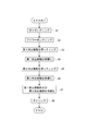
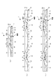
- 5 is a flowchart showing a manufacturing operation of a semiconductor device. It is explanatory drawing which showed the manufacturing operation of the semiconductor device. It is sectional drawing which showed typically the 1st modification (a) and 2nd modification (b) of a semiconductor device. It is sectional drawing which showed typically the 3rd modification (a) of a semiconductor device, the 4th modification (b), the 5th modification (c), and the 6th modification (d). It is sectional drawing which showed typically the 7th modification (a) of a semiconductor device, the 8th modification (b), and the 9th modification (c).
- This semiconductor device is a lead frame type semiconductor light receiving device (package) on which a light receiving element is mounted, and is used for, for example, a light receiving IC, an illuminance sensor, a color sensor, and the like.
- this semiconductor device achieves high light transmittance and high adhesion of the sealing resin by using two types of sealing resins.
- the light receiving side is defined as the front surface side
- the opposite side is defined as the back surface side. The description will be made with the front side of the semiconductor device as the upper side and the back side as the lower side.
- the semiconductor device 1 seals a lead frame 11, a light receiving element (photoelectric conversion element) 12 mounted on the lead frame 11, and the lead frame 11 (surface and frame gap 35).
- 1 sealing resin 13 and 2nd sealing resin 14 which seals the light receiving element 12 are provided.
- the first sealing resin 13 and the second sealing resin 14 are potted over the entire lead frame 11 from the surface side, and the interface between the first sealing resin 13 and the second sealing resin 14 Located in the middle height position.
- FIG. 1B illustration of the first sealing resin 13 and the second sealing resin 14 is omitted.
- the light receiving element 12 is an element that has a light receiving region 21 on its surface and converts received light into an electrical signal. Further, a plurality of contacts 22 (electrode pads) of the gold wire W are formed on the outer surface of the light receiving element 12. By the wire bonding, the plurality of contacts 22 and the plurality of lead portions 34 of the lead frame 11 are connected by the gold wire W, so that the light receiving element 12 and each lead portion 34 of the lead frame 11 are electrically connected.
- the lead frame 11 includes a frame portion 31, a mount portion 32 that is supported by the frame portion 31 and on which the light receiving element 12 is mounted, and a plurality of leads that are supported by the frame portion 31 and each have a contact 33 of a gold wire W. Part 34.
- the lead frame 11 is formed by subjecting a conductive flat plate made of copper to punching (die cutting or etching) to form a frame portion 31, a mount portion 32, and a lead portion 34.
- the extracted portion of the lead frame 11 is referred to as a frame gap 35.
- the lead frame 11 has a front surface (one surface on the front and back) as a mounting surface for the light receiving element 12 and a back surface (the other surface on the front and back) as a solder surface. That is, the light receiving element 12 is bonded to the surface of the mount portion 32.
- the lead frame 11 is subjected to a gold plating process (for example, Ni—Pd—Au or the like), and a predetermined region of each lead part 34 subjected to the gold plating process becomes a contact 33 of the gold wire W.
- a gold plating process for example, Ni—Pd—Au or the like
- 1st sealing resin 13 is comprised with the opaque epoxy resin (opaque epoxy resin material) which added the filler, and the glass transition temperature is over 120 degreeC.
- the first sealing resin 13 is made of a potting resin material, and is potted to fill the frame gap 35 of the lead frame 11 and cover the surface of the lead frame 11. That is, the first sealing resin 13 seals the entire surface of the lead frame 11 and the frame gap 35. Furthermore, the lower end surface of the first sealing resin 13 is flush with the back surface of the lead frame 11, and the upper end surface of the first sealing resin 13 is higher than the surface of the lead frame 11 and lower than the surface of the light receiving element 12. ing. That is, the first sealing resin 13 is molded so that the light receiving region 21 of the light receiving element 12 is exposed.
- the second sealing resin 14 is made of a transparent epoxy resin (transparent epoxy resin material) and has a transmittance of 90% or more.
- the second sealing resin 14 is made of a potting resin material and is potted so as to seal the light receiving element 12 and cover the surface of the first sealing resin 13. That is, the second sealing resin 14 seals the exposed portion (including the light receiving region 21) of the light receiving element 12 exposed from the first sealing resin 13. Therefore, the upper end surface of the second sealing resin 14 is higher than the surface of the light receiving element 12.
- the first sealing resin 13 and the second sealing resin 14 are formed after wire bonding of the light receiving element 12 to the lead frame 11.
- the “transmittance” here refers to the visible light transmittance when the received light is visible light, and refers to the ultraviolet transmittance when the received light is ultraviolet light.
- the manufacturing operation of the semiconductor device 1 will be described with reference to FIGS.
- a plurality of large-sized lead frames 11 are processed as they are in this state, and then divided (divided) into the respective semiconductor devices 1.
- the manufacturing operation is performed in a state where the lead frame 11 is subjected to the above plating process and the back tape T is adhered to the entire back surface (see FIG. 3A).
- the back tape T is a polyimide tape (heat resistant tape) and is also used as a positioning tape.
- die bonding of the light receiving element 12 is performed on the lead frame 11 (S1: die bonding step). That is, a die attach agent is applied to the surface of the mount portion 32 of the lead frame 11 (see FIG. 3B), and after the light receiving element 12 is disposed on the die attach agent, the die attach agent is cured (FIG. 3 ( c)). As a result, the light receiving element 12 is fixed (mounted) to the mount portion 32.
- wire bonding of the light receiving element 12 is performed on the lead frame 11 (S2: wire bonding step). That is, each contact 22 of the light receiving element 12 and each contact 33 of each lead portion 34 of the lead frame 11 are connected by the gold wire W, and both are electrically connected (see FIG. 3D).
- the first sealing resin 13 is potted (S3: first potting step). That is, the first sealing resin 13 is potted (entirely) over the entire area of the lead frame 11 including the frame gap 35, and is received up to the intermediate height position of the light receiving element 12 by receiving the back tape T (FIG. 3 ( e)). Thus, the first sealing resin 13 fills (seals) the frame gap 35 of the lead frame 11 and seals the entire surface of the lead frame 11. At this time, the light receiving region 21 of the light receiving element 12 is exposed from the first sealing resin 13.
- the potted first sealing resin 13 is temporarily cured (S4: first temporary curing step). Specifically, the first sealing resin 13 is cured by heating at 135 ° C. for 30 minutes. In addition, this temporary hardening is a thing of the grade which hardens the surface of the 1st sealing resin 13 so that it may not mix with the 2nd sealing resin 14 potted.
- the second sealing resin 14 is potted in a state where the first sealing resin 13 is temporarily cured (S5: second potting step). That is, the second sealing resin 14 is entirely potted on the light receiving element 12 and the first sealing resin 13 and deposited to a position higher than the light receiving region 21 (see FIG. 3F). Thereby, the second sealing resin 14 seals the light receiving region 21.
- the potted second sealing resin 14 is temporarily cured (S6: second temporary curing step). Specifically, like the first sealing resin 13, the second sealing resin 14 is thermally cured by heating at 135 ° C. for 30 minutes.
- the first resin molding step includes a first potting step, a first temporary curing step, and a main curing step
- the second resin molding step includes a second potting step, a second temporary curing step, and a main curing step. Has been.
- an existing potting device can be used by molding the two types of sealing resins 13 and 14 by potting, and molding can be performed with inexpensive equipment. Further, since it is not necessary to form the lead frame 11 as a substrate, the semiconductor device 1 can be easily manufactured without requiring deburring or the like. Further, by molding the two types of sealing resins 13 and 14, it is possible to use the sealing resins 13 and 14 suitable for the sealing of the lead frame 11 and the sealing of the light receiving region 21. That is, for the first sealing resin 13, a resin material can be freely selected without restriction (for example, light transmittance) related to light reception.
- a resin material can be freely selected for the second sealing resin 14 without any restrictions (for example, adhesion, thermal deformation, and heat dissipation) related to the sealing of the lead frame 11.
- any restrictions for example, adhesion, thermal deformation, and heat dissipation
- sufficient adhesion can be obtained by using suitable sealing resins 13 and 14.
- an opaque resin material as the first sealing resin 13
- a resin material having high adhesion to the lead frame 11 can be used.
- the opaque resin is arranged so as to surround the light receiving region 21 in a plan view. As a result, stray light can be prevented during light reception, and light reception accuracy can be improved.
- the heat deformability of the first sealing resin 13 can be suppressed.
- the first sealing resin 13 is molded so as to seal the entire surface of the lead frame 11, thereby potting the first sealing resin 13 over the entire area of the lead frame 11. . That is, since the first sealing resin 13 can be applied to the entire area of the lead frame 11, potting can be performed without requiring complicated device control. In addition, since the second sealing resin 14 is in close contact with the first sealing resin 13 without being in close contact with the lead frame 11, peeling of the second sealing resin 14 can be prevented.
- the solder surface of the semiconductor device 1 is not uneven. (Jointability) can be improved.
- the first sealing resin 13 is potted after wire bonding, it is not necessary to avoid the contact 33 of the gold wire W of the lead frame 11, so the first sealing resin 13 is molded. It can be done easily.
- the potted first sealing resin 13 is temporarily cured, and the second sealing resin 14 is potted in that state, so that the potted first sealing resin 13 and the second sealing resin 13 are sealed.
- the stop resin 14 can be fully cured as a unit. That is, since it is not necessary to perform the main curing with each of the first sealing resin 13 and the second sealing resin 14, it is possible to reduce the time in the manufacturing process.
- the 1st sealing resin 13 and the 2nd sealing resin 14 were comprised with the epoxy-type resin material, it does not restrict to this. That is, the first sealing resin 13 may be made of an epoxy resin material, the second sealing resin 14 may be made of a silicon resin material, or the first sealing resin 13 may be made of a silicon resin material. The second sealing resin 14 may be made of an epoxy resin material. Moreover, you may comprise the 1st sealing resin 13 and the 2nd sealing resin 14 with a silicon-type resin material.
- the first sealing resin 13 is formed after wire bonding.
- the first sealing resin 13 may be formed before wire bonding. In such a case, the first sealing resin 13 is molded while avoiding the contact 33 of each lead part 34.
- the first sealing resin 13 is deposited up to the intermediate height position of the light receiving element 12, but the first sealing resin 13 is disposed at least in the frame gap 35 of the lead frame 11.
- the present invention is not limited to this as long as it is configured to fill (close) and expose the light receiving region 21.
- the first sealing resin 13 is molded such that the frame gap 35 is filled (closed) and its upper end surface is lower than the surface of the lead frame 11. May be.
- the first sealing resin 13 may be deposited beyond the height of the light receiving region 21. In such a case, in order to expose the light receiving area 21, the light receiving area 21 is formed so as to avoid the light receiving area 21.
- the potted sealing resin 13 it is preferable to prevent the potted sealing resin 13 from flowing into the light receiving region 21 by utilizing the surface tension of the first sealing resin 13.
- a thin film (not shown) is formed in a portion other than the light receiving region 21 and the light receiving region 21 is made lower than the other portions. As a result, it is possible to prevent the first sealing resin 13 from flowing into the light receiving region 21 due to surface tension acting at the level difference between the thin film surface and the light receiving region 21 during molding.
- the present invention is applied to the semiconductor device 1 using the lead frame 11 having the mount portion 32, but the present invention is applied to the semiconductor device 1 using the lead frame 11 not having the mount portion 32. May be applied.
- the light receiving element 21 is bonded (fixed) on the lead portion 34, but instead of the die attach agent, the light receiving element 12 is bonded by the DAF tape 41 (see FIG. 5A),
- the structure (refer FIG.5 (b)) which adheres the light receiving element 12 with the adhesive agent 42 of an insulating paste can be considered.
- the first sealing resin 13 may be molded such that its upper end surface is lower than the surface of the lead frame 11 (FIG. 5 ( c) and (d)).
- the present invention is applied to the semiconductor device 1 (semiconductor light-receiving device) on which the light-receiving element 12 is mounted.
- the present invention may be applied to the semiconductor device 1 (semiconductor light emitting device) on which the conversion element 52 is mounted.
- the first sealing resin 13 is molded so as to expose the light emitting region 51 of the light emitting element 52, and the second sealing resin 14 seals the light emitting region 51 of the light emitting element 52.
- the first sealing resin 13 is made of an opaque resin material, so that the emitted light can have directivity (spot).
- the present invention may be applied to a two-chip type semiconductor device 1 in which the light receiving element 12 and the light emitting element 52 are mounted.
- the first sealing resin 13 is molded so as to expose the light receiving region 21 and the light emitting region 51
- the second sealing resin 14 seals the light receiving region 21 and the light emitting region 51.
- the first sealing resin 13 is deposited beyond the height of the light receiving region 21, and the light receiving region 21 is avoided.
- molds may be sufficient (refer FIG.6 (c)).
- the light emitting element 52 forms the light emitting region 51 at a position higher than the surface of the first sealing resin 13 to be molded. According to this configuration, since the light receiving region 21 is formed to be lower than the surface of the first sealing resin 13 and the first sealing resin 13 surrounds the light receiving region 21, the irradiation light from the light emitting region 52 is not emitted.
- the semiconductor device 1 can be manufactured more easily.
- the first sealing resin 13 is molded so as to fill the frame gap 35 and its upper end surface is lower than the surface of the lead frame 11, as in FIG. 4A. It may be configured to do so.
- the mounting structure of the light receiving element 21 and / or the light emitting element 51 may be the same mounting structure as that of FIGS. That is, even when the lead frame 11 having no mount is used, the light receiving element 21 and / or the light emitting element 51 are bonded (adhered) to the lead frame 11 by the DAF tape 41 or the adhesive 42 of the insulating paste. good.
- a configuration in which two or more light receiving elements 12 and / or light emitting elements 52 are mounted. May be.
Landscapes
- Led Device Packages (AREA)
- Structures Or Materials For Encapsulating Or Coating Semiconductor Devices Or Solid State Devices (AREA)
Abstract
本発明は、リードフレームの封止および受発光領域の封止のそれぞれに対し好適な封止樹脂を用いることができると共に、安価な設備で且つ容易に製造可能な半導体装置を提供することを課題としている。 本発明は、受光領域21を有した受光素子12と、受光素子12を表面に搭載し、裏面を半田面とするリードフレーム11と、ポッティング樹脂材料で構成され、少なくともリードフレーム11のフレーム間隙35に充填され、且つ受光領域21が露出するように成形された第1封止樹脂13と、第1封止樹脂13と異なるポッティング樹脂材料で構成され、ポッティングにより、少なくとも受光領域21を封止するように成形された第2封止樹脂14と、を備えたことを特徴とする。
Description
本発明は、受光素子や発光素子等の光電変換素子を搭載した半導体装置および半導体装置の製造方法に関するものである。
従来、この種の半導体装置として、リードフレームから製造された平坦回路基板と、平坦回路基板のダイパッドに搭載した光電変換素子と、光電変換素子を封止する透明樹脂と、を備えたものが記載されている(特許文献1参照)。この平坦回路基板は、リードフレームの除去部に、熱硬化性樹脂を充填して製造されている。これにより、安価で製品設計変更が容易であり、しかも熱伝導性に優れた平坦回路基板を提供することができる。
しかしながら、このような構成では、リードフレームを金型で挟んだ状態で熱硬化性樹脂を充填する薄型のインサート成形(トランスファー成形)により、回路基板を製造するため、金型が必要な上、半導体装置の製造工程全体が煩雑になってしまうという問題があった。すなわち、ダイボンディング工程、ワイヤーボンディング工程、および透明樹脂成形工程に加え、熱硬化性樹脂のインサート成形工程と、成形した熱硬化性樹脂のバリ取り工程とを実行して、リードフレームを基板化する必要がある。そのため、製造工程が複雑化してしまう。
これに対し、単一の透明樹脂(例えば透明エポキシ樹脂)によって、リードフレームおよび光電変換素子を一体で封止することも可能であるが、かかる場合、リードフレームを封止するのに適した樹脂材料を用いることができないため、密着性や熱変形性、放熱性等に問題が生じた。具体的には、リードフレームと透明樹脂とでは密着性が低くなるため、リードフレームの除去部内面と透明樹脂との間から搭載面側に半田が侵入し、光電変換素子等に不良を生じさせるという問題が生ずる。または、成形した透明樹脂が熱変形し、リードフレームと透明樹脂との間に間隙ができてしまうという問題が生ずる。
これに対し、単一の透明樹脂(例えば透明エポキシ樹脂)によって、リードフレームおよび光電変換素子を一体で封止することも可能であるが、かかる場合、リードフレームを封止するのに適した樹脂材料を用いることができないため、密着性や熱変形性、放熱性等に問題が生じた。具体的には、リードフレームと透明樹脂とでは密着性が低くなるため、リードフレームの除去部内面と透明樹脂との間から搭載面側に半田が侵入し、光電変換素子等に不良を生じさせるという問題が生ずる。または、成形した透明樹脂が熱変形し、リードフレームと透明樹脂との間に間隙ができてしまうという問題が生ずる。
本発明は、リードフレームの封止および受発光領域の封止のそれぞれに対し好適な封止樹脂を用いることができると共に、安価な設備で且つ容易に製造することができる半導体装置および半導体装置の製造方法を提供することを課題としている。
本発明の半導体装置は、受光領域および発光領域の少なくとも一方である受発光領域を有した光電変換素子と、光電変換素子を表裏一方の面に搭載し、表裏他方の面を半田面とするリードフレームと、ポッティング樹脂材料で構成され、少なくともリードフレームのフレーム間隙に充填され、且つ受発光領域が露出するように成形された第1封止樹脂と、第1封止樹脂と異なるポッティング樹脂材料で構成され、少なくとも受発光領域を封止するように成形された第2封止樹脂と、を備えたことを特徴とする。
本発明の半導体装置の製造方法は、受光領域および発光領域の少なくとも一方である受発光領域を有した光電変換素子と、光電変換素子を表裏一方の面に搭載し、表裏他方の面を半田面とするリードフレームと、材料が異なる第1封止樹脂および第2封止樹脂と、を備えた半導体装置の製造方法であって、光電変換素子を、リードフレームに搭載するダイボンディング工程と、ポッティングにより、第1封止樹脂を、少なくともリードフレームのフレーム間隙に充填され、且つ受発光領域が露出するように成形する第1樹脂成形工程と、ポッティングにより、第2封止樹脂を、受発光領域を封止するように成形する第2樹脂成形工程と、を実行することを特徴とする。
これらの構成によれば、ポッティングにより、リードフレーム封止用の第1封止樹脂と、受発光領域封止用の第2封止樹脂との2種の封止樹脂とを成形する。このように、2種の封止樹脂をポッティングにより成形することで、既存のポッティング装置を用いることができ、安価な設備で成形することができる。また、リードフレームを基板化する必要がないため、バリ取り等を必要とせず、半導体装置を容易に製造することができる。さらに、2種の封止樹脂を成形することで、リードフレームの封止および受発光領域の封止のそれぞれに対し好適な封止樹脂を用いることができる。すなわち、第1封止樹脂について、受発光に係る制約(例えば光透過性)なしに、自由に樹脂材料を選出することができる。一方、第2封止樹脂について、リードフレームの封止に係る制約(例えば密着性、熱変形性や放熱性)なしに、自由に樹脂材料を選出することができる。なお、第1封止樹脂上に、第2封止樹脂を成形するようにしても良い。
上記の半導体装置において、第1封止樹脂は、不透明樹脂材料で構成されており、第2封止樹脂は、透明樹脂材料で構成されていることが好ましい。
この構成によれば、第1封止樹脂として不透明樹脂材料を用いることで、リードフレームに対し密着性の高い樹脂材料を用いることができる。また、平面視において、受発光領域を囲うように不透明樹脂が配置される構成となる。その結果、受発光領域が受光領域である場合には、迷光を防止することができ、受光精度を向上することができる。一方、受発光領域が発光領域である場合には、発光した光に指向性を持たせる(スポットさせる)ことができる。なお、第1封止樹脂について、迷光防止や指向性を持たせるのに適した色(例えば黒色)の樹脂材料を用いるようにしても良い。
上記の半導体装置において、第1封止樹脂および第2封止樹脂は、エポキシ系樹脂材料で構成されていることが好ましい。
この構成によれば、両封止樹脂に、安価なエポキシ系樹脂材料を用いることで、コストダウンを図ることができる。
上記の半導体装置において、第1封止樹脂は、エポキシ系樹脂材料で構成されており、第2封止樹脂は、シリコン系樹脂材料で構成されていることが好ましい。
この構成によれば、第1封止樹脂に、密着性の高いエポキシ系樹脂材料を用い、第2封止樹脂に、光透過性の高いシリコン系樹脂材料を用いることで、リードフレームに対する封止の高い密着性と、受発光領域に対する封止の高い光透過性とを得ることができる。また、第1封止樹脂に、安価なエポキシ系樹脂材料を用いることで、コストダウンを図ることができる。一方で、第2封止樹脂に、耐熱性の高いシリコン系樹脂を用いることで、受発光領域の発熱による、第2封止樹脂の熱劣化を回避することができる。
上記の半導体装置において、第1封止樹脂は、シリコン系樹脂材料で構成されており、第2封止樹脂は、エポキシ系樹脂材料で構成されていることが好ましい。
リードフレーム表面を第2封止樹脂により封止する場合、第2封止樹脂に高いガスバリア性が求められるケースがある。例えば、リードフレーム表面に、内装メッキとして部分Agメッキを施すケースでは、ガスバリア性が悪いシリコン系樹脂材料を第2封止樹脂に用いると、空気中の硫黄ガスが銀と硫化反応してしまう。
これに対し、上記の構成によれば、エポキシ系樹脂材料を第2封止樹脂に用いることで、リードフレーム表面の部分Agメッキに対し、十分なガスバリア性を確保することができる。よって、空気中の硫黄ガスが銀と硫化反応してしまうのを防止することができる。
これに対し、上記の構成によれば、エポキシ系樹脂材料を第2封止樹脂に用いることで、リードフレーム表面の部分Agメッキに対し、十分なガスバリア性を確保することができる。よって、空気中の硫黄ガスが銀と硫化反応してしまうのを防止することができる。
上記の半導体装置において、第1封止樹脂および第2封止樹脂は、シリコン系樹脂材料で構成されていることが好ましい。
この構成によれば、両封止樹脂に、耐熱性の高いシリコン系樹脂材料を用いることで、両封止樹脂の熱変形や熱劣化を抑えることができる。特に、受発光領域の発熱による、第2封止樹脂の熱劣化を回避することができる。
上記の半導体装置において、第1封止樹脂は、ガラス転移温度が100℃超の樹脂材料で構成されていることが好ましい。
この構成によれば、第1封止樹脂の熱変形性を抑えることができる。なお、第1封止樹脂は、ガラス転移温度が120℃超の樹脂材料で構成されていることがさらに好ましい。
上記の半導体装置において、第1封止樹脂は、フィラーを添加した樹脂材料で構成されていることが好ましい。
この構成によれば、第1封止樹脂の熱変形性を抑え、且つ放熱性を向上することができる。
上記の半導体装置において、第1封止樹脂は、リードフレームの上記表裏一方の面全域を封止するように成形されることが好ましい。
この構成によれば、第1封止樹脂をリードフレームの全域にポッティングする構成となる。すなわち、第1封止樹脂をリードフレーム全域に塗布することができるため、複雑な装置制御を必要とせずに、ポッティングを行うことができる。また、第2封止樹脂を、リードフレームに密着させず、第1封止樹脂に密着させる構成となるため、第2封止樹脂の剥がれを防止することができる。
上記の半導体装置において、第1封止樹脂は、リードフレームの表裏他方の面と面一となるように成形されることが好ましい。
この構成によれば、半導体装置の半田面に凹凸が生じないため、半導体装置の実装性(接合性)を向上することができる。
上記の半導体装置において、光電変換素子をn(n≧2)個備え、n個の光電変換素子のうちのm(n>m≧1)個の光電変換素子は、受発光領域として、受光領域を有し、n個の光電変換素子のうちの(n-m)個の光電変換素子は、受発光領域として、発光領域を有することが好ましい。
この構成によれば、受光素子および発光素子をそれぞれ1個以上搭載した多チップ型の半導体装置を、安価な設備で且つ容易に製造することができる。なお、当該多チップ型の半導体装置としては、反射型光センサー等が想定される。
この場合、第1封止樹脂は、m個の光電変換素子の受光領域の高さを超えて堆積されると共に、受光領域を避けて成形され、(n-m)個の光電変換素子は、成形された第1封止樹脂の表面より高い位置に、発光領域を有していることが好ましい。
この構成によれば、受光領域が第1封止樹脂の表面のより低くなり且つ第1封止樹脂が受光領域を囲うように成形されるため、発光領域からの照射光が、第2封止樹脂の表面で反射して、受光領域に入射するのを好適に防止することができる。すなわち、受光領域と発光領域との間に、特段の遮光部材を設ける必要がないため、半導体装置をさらに容易に製造することができる。
上記の半導体装置において、第1封止樹脂は、リードフレームに対し光電変換素子のワイヤーボンディングを行った後に成形されることが好ましい。
上記の半導体装置の製造方法において、リードフレームに対し、搭載した光電変換素子のワイヤーボンディングを行うワイヤーボンディング工程と、を更に実行し、第1樹脂成形工程を、ワイヤーボンディング工程の後に実行することが好ましい。
ワイヤーボンディングの前に第1封止樹脂を成形する場合、リードフレーム側の金線の接点を避けて成形を行う必要がある。そのため、第1封止樹脂の成形が煩雑になってしまう。仮にフレーム間隙のみに第1封止樹脂を成形する場合であっても、フレーム間隙からはみ出さずに第1封止樹脂を成形するのは煩雑であり、同様の問題が生じる。
これに対し、上記構成によれば、リードフレームの金線の接点を避けて成形を行う必要がないため、第1封止樹脂の成形を容易に行うことができる。
これに対し、上記構成によれば、リードフレームの金線の接点を避けて成形を行う必要がないため、第1封止樹脂の成形を容易に行うことができる。
上記の半導体装置において、第1樹脂成形工程では、第1封止樹脂をポッティングする第1ポッティング工程を、実行し、第2樹脂成形工程では、第1ポッティング工程によりポッティングした第1封止樹脂が仮硬化した状態で、第2封止樹脂をポッティングする第2ポッティング工程を、実行することが好ましい。
この構成によれば、ポッティングした第1封止樹脂を仮硬化し、その状態で第2封止樹脂をポッティングすることで、ポッティングした第1封止樹脂および第2封止樹脂を、一体として本硬化することができる。すなわち、第1封止樹脂および第2封止樹脂のそれぞれで、本硬化を行う必要がないため、製造工程における時間短縮を行うことができる。
以下、添付の図面を参照して、本発明の一実施形態に係る半導体装置および半導体装置の製造方法について説明する。本実施形態では、本発明を適用した半導体装置を例示する。この半導体装置は、受光素子を搭載したリードフレームタイプの半導体受光装置(パッケージ)であり、例えば、受光ICや、照度センサー、カラーセンサー等に用いられる。特に、本半導体装置は、2種の封止樹脂を用いることで、高い光透過性と、封止樹脂の高い密着性とを実現している。なお、以下の説明では、半導体装置において、光を受光する側を表面側とし、その逆側を裏面側とする。また、半導体装置の表面側を上とし、裏面側を下として説明する。
図1に示すように、半導体装置1は、リードフレーム11と、リードフレーム11に搭載された受光素子(光電変換素子)12と、リードフレーム11(の表面およびフレーム間隙35)を封止する第1封止樹脂13と、受光素子12を封止する第2封止樹脂14と、を備えている。第1封止樹脂13および第2封止樹脂14は、表面側からリードフレーム11全域にポッティング成形されており、第1封止樹脂13および第2封止樹脂14の界面は、受光素子12の中間高さ位置に位置している。なお、図1(b)では、第1封止樹脂13および第2封止樹脂14の図示を省略している。
受光素子12は、その表面に受光領域21を有し、受光した光を電気信号に変換する素子である。また、受光素子12の表面外側には、金線Wの接点22(電極パッド)が複数形成されている。ワイヤーボンディングにより、当該複数の接点22とリードフレーム11の複数のリード部34とが金線Wで結線されることで、受光素子12とリードフレーム11の各リード部34とが電気的に接続される。
リードフレーム11は、枠部31と、枠部31に支持されると共に受光素子12が搭載されるマウント部32と、枠部31に支持されると共に金線Wの接点33をそれぞれ有する複数のリード部34と、を有している。リードフレーム11は、銅を材料とする導体平板に、抜き加工(型抜きまたはエッチング抜き)を施して、枠部31、マウント部32およびリード部34を形成したものである。なお、以下、リードフレーム11の当該抜き部分をフレーム間隙35と呼称する。
また、リードフレーム11は、表面(表裏一方の面)を受光素子12の搭載面とし、裏面(表裏他方の面)を半田面としている。すなわち、マウント部32の表面に、受光素子12がボンディングされる。リードフレーム11には、金メッキ処理(例えば、Ni-Pd-Au等)が施されており、この金メッキ処理が施された各リード部34の所定領域が、金線Wの接点33となる。
第1封止樹脂13は、フィラーを添加した不透明エポキシ樹脂(不透明のエポキシ系樹脂材料)で構成されており、ガラス転移温度が120℃超となっている。また、第1封止樹脂13は、ポッティング樹脂材料で構成されており、リードフレーム11のフレーム間隙35に充填され、且つリードフレーム11の表面を覆うように、ポッティング成形されている。すなわち、第1封止樹脂13は、リードフレーム11の表面全域およびフレーム間隙35を封止している。さらに、第1封止樹脂13の下端面は、リードフレーム11の裏面と面一となり、第1封止樹脂13の上端面は、リードフレーム11の表面より高く且つ受光素子12の表面より低くなっている。すなわち、第1封止樹脂13は、受光素子12の受光領域21が露出するように成形されている。
第2封止樹脂14は、透明エポキシ樹脂(透明のエポキシ系樹脂材料)で構成されており、透過率が90%以上となっている。また、第2封止樹脂14は、ポッティング樹脂材料で構成されており、受光素子12を封止し、且つ第1封止樹脂13の表面を覆うように、ポッティング成形されている。すなわち、第2封止樹脂14は、第1封止樹脂13から露出した受光素子12の露出部分(受光領域21を含む)を封止している。よって、第2封止樹脂14の上端面は、受光素子12の表面より高くなっている。なお、第1封止樹脂13および第2封止樹脂14は、リードフレーム11に対し受光素子12のワイヤーボンディングを行った後に成形される。また、ここにいう「透過率」とは、受光する光が可視光である場合には、可視光透過率を指し、受光する光が紫外線である場合には、紫外線透過率を指す。
次に図2および図3を参照して、半導体装置1の製造動作について説明する。本製造動作は、複数個取りの大判のリードフレーム11を、その状態のまま一体として加工した後、各半導体装置1に分断(分割)するものである。また、本製造動作は、リードフレーム11に上記メッキ処理が施され、且つ裏面全体にバックテープTが貼着された状態で行われる(図3(a)参照)。なお、このバックテープTは、ポリイミドテープ(耐熱テープ)であり、位置決めテープとしても用いられる。
図2に示すように、まず、リードフレーム11に対し、受光素子12のダイボンディングを行う(S1:ダイボンディング工程)。すなわち、リードフレーム11のマウント部32表面に、ダイアタッチ剤を塗布し(図3(b)参照)、ダイアタッチ剤上に受光素子12を配置した後、ダイアタッチ剤を硬化させる(図3(c)参照)。これにより、受光素子12がマウント部32に固着(搭載)される。
次に、リードフレーム11に対し、受光素子12のワイヤーボンディングを行う(S2:ワイヤーボンディング工程)。すなわち、受光素子12の各接点22と、リードフレーム11の各リード部34の接点33と、金線Wによりそれぞれ結線し、両者を電気的に接続する(図3(d)参照)。
ワイヤーボンディングが終了したら、第1封止樹脂13をポッティングする(S3:第1ポッティング工程)。すなわち、第1封止樹脂13を、フレーム間隙35を含むリードフレーム11全域に(全体的に)ポッティングし、バックテープTを受けとして、受光素子12の中間高さ位置まで堆積させる(図3(e)参照)。これにより、第1封止樹脂13が、リードフレーム11のフレーム間隙35を充填(封止)すると共に、リードフレーム11の表面全域を封止する。また、このとき、第1封止樹脂13から、受光素子12の受光領域21が露出した状態となる。
第1封止樹脂13のポッティングが終了したら、ポッティングした第1封止樹脂13の仮硬化を行う(S4:第1仮硬化工程)。具体的には、135℃で30分加熱して、第1封止樹脂13を熱硬化させる。なお、本仮硬化は、ポッティングされる第2封止樹脂14と混ざらないように、第1封止樹脂13の表面を硬化させる程度のものである。
その後、第1封止樹脂13が仮硬化した状態で、第2封止樹脂14をポッティングする(S5:第2ポッティング工程)。すなわち、第2封止樹脂14を、受光素子12および第1封止樹脂13上に全体的にポッティングし、受光領域21より高い位置まで堆積させる(図3(f)参照)。これにより、第2封止樹脂14が、受光領域21を封止する。
第2封止樹脂14のポッティング成形が終了したら、ポッティングした第2封止樹脂14の仮硬化を行う(S6:第2仮硬化工程)。具体的には、第1封止樹脂13と同様、135℃で30分加熱して、第2封止樹脂14を熱硬化させる。
その後、第1封止樹脂13および第2封止樹脂14の本硬化を行う(S7:本硬化工程)。具体的には、バックテープTを剥離した後、160℃で2時間加熱して、第1封止樹脂13および第2封止樹脂14を硬化させる(図3(g)参照)。なお、第1樹脂成形工程は、第1ポッティング工程、第1仮硬化工程および本硬化工程により構成され、第2樹脂成形工程は、第2ポッティング工程、第2仮硬化工程および本硬化工程により構成されている。
最後に、ダイシング(分断)を行い(S8:ダイシング工程)、複数の半導体装置1に得る(図3(h)参照)。これにより本動作を終了する。
以上のような構成によれば、2種の封止樹脂13、14をポッティングにより成形することで、既存のポッティング装置を用いることができ、安価な設備で成形することができる。また、リードフレーム11を基板化する必要がないため、バリ取り等を必要とせず、半導体装置1を容易に製造することができる。さらに、2種の封止樹脂13、14を成形することで、リードフレーム11の封止および受光領域21の封止のそれぞれに対し好適な封止樹脂13、14を用いることができる。すなわち、第1封止樹脂13について、受光に係る制約(例えば光透過性)なしに、自由に樹脂材料を選出することができる。一方、第2封止樹脂14について、リードフレーム11の封止に係る制約(例えば密着性、熱変形性や放熱性)なしに、自由に樹脂材料を選出することができる。特に、リードフレーム11にメッキ処理(金メッキ)が施されていたとしても、好適な封止樹脂13、14を用いることより、十分な密着性を得ることができる。
また、第1封止樹脂13として不透明樹脂材料を用いることで、リードフレーム11に対し密着性の高い樹脂材料を用いることができる。また、平面視において、受光領域21を囲うように不透明樹脂が配置される構成となる。その結果、受光に際し、迷光を防止することができ、受光精度を向上することができる。
さらに、両封止樹脂に、安価なエポキシ系樹脂材料を用いることで、コストダウンを図ることができる。
またさらに、第1封止樹脂13に、ガラス転移温度が100℃超(ひいては120℃超)の樹脂材料を用いることで、第1封止樹脂13の熱変形性を抑えることができる。
また、第1封止樹脂13に、フィラーを添加した樹脂材料を用いることで、第1封止樹脂13の熱変形性を抑え、且つ放熱性を向上することができる。
さらに、本実施形態において、第1封止樹脂13を、リードフレーム11の表面全域を封止するように成形することで、第1封止樹脂13をリードフレーム11の全域にポッティングする構成となる。すなわち、第1封止樹脂13をリードフレーム11全域に塗布することができるため、複雑な装置制御を必要とせずに、ポッティングを行うことができる。また、第2封止樹脂14を、リードフレーム11に密着させず、第1封止樹脂13に密着させる構成となるため、第2封止樹脂14の剥がれを防止することができる。
またさらに、第1封止樹脂13の下端面が、リードフレーム11の裏面と面一になるように成形させることで、半導体装置1の半田面に凹凸が生じないため、半導体装置1の実装性(接合性)を向上することができる。
また、第1封止樹脂13を、ワイヤーボンディングの後にポッティング成形することで、リードフレーム11の金線Wの接点33を避けて成形を行う必要がないため、第1封止樹脂13の成形を容易に行うことができる。
さらに、半導体装置1の製造動作において、ポッティングした第1封止樹脂13を仮硬化し、その状態で第2封止樹脂14をポッティングすることで、ポッティングした第1封止樹脂13および第2封止樹脂14を、一体として本硬化することができる。すなわち、第1封止樹脂13および第2封止樹脂14のそれぞれで、本硬化を行う必要がないため、製造工程における時間短縮を行うことができる。
なお、本実施形態においては、第1封止樹脂13および第2封止樹脂14を、エポキシ系樹脂材料で構成したが、これに限るものではない。すなわち、第1封止樹脂13を、エポキシ系樹脂材料で構成し、第2封止樹脂14を、シリコン系樹脂材料で構成しても良いし、第1封止樹脂13を、シリコン系樹脂材料で構成し、第2封止樹脂14を、エポキシ系樹脂材料で構成しても良い。また、第1封止樹脂13および第2封止樹脂14を、シリコン系樹脂材料で構成しても良い。
また、本実施形態においては、ワイヤーボンディングの後に第1封止樹脂13を成形する構成であったが、ワイヤーボンディングの前に第1封止樹脂13を成形する構成であっても良い。かかる場合、各リード部34の接点33を避けて、第1封止樹脂13を成形する。
さらに、本実施形態においては、第1封止樹脂13を、受光素子12の中間高さ位置まで堆積させる構成であったが、第1封止樹脂13を、少なくともリードフレーム11のフレーム間隙35を充填(閉塞)し且つ受光領域21が露出するように成形する構成であれば、これに限るものではない。例えば、図4(a)に示すように、第1封止樹脂13を、フレーム間隙35を充填(閉塞)し且つその上端面がリードフレーム11の表面より低くなるように、成形する構成であっても良い。また、例えば、図4(b)に示すように、第1封止樹脂13を、受光領域21の高さを超えて堆積させる構成であっても良い。かかる場合、受光領域21を露出させるべく、平面内で受光領域21を避けて成形する。このとき、第1封止樹脂13の表面張力を利用して、ポッティングした封止樹脂13が受光領域21に流れ込まないようにすることが好ましい。例えば、受光領域21の以外の部分に、薄膜(図示省略)を形成し、受光領域21を他の部分に比して低くしておく。これにより、成形に際し、薄膜表面と受光領域21との段差において、表面張力が作用し、第1封止樹脂13が受光領域21に流れ込むのを防止することができる。
またさらに、本実施形態においては、マウント部32を有したリードフレーム11を用いる半導体装置1に、本発明を適用したが、マウント部32を有しないリードフレーム11を用いる半導体装置1に、本発明を適用しても良い。かかる場合、受光素子21をリード部34上に接着(固着)する構成となるが、ダイアタッチ剤に代えて、DAFテープ41により受光素子12を接着する構成(図5(a)参照)や、絶縁ペーストの接着剤42により受光素子12を接着する構成(図5(b)参照)が考えられる。また当該両構成において、図4(a)と同様、第1封止樹脂13を、その上端面がリードフレーム11の表面より低くとなるように、成形する構成であっても良い(図5(c)および(d)参照)。
また、本実施形態においては、受光素子12を搭載した半導体装置1(半導体受光装置)に、本発明を適用したが、図6(a)に示すように、発光領域51を有する発光素子(光電変換素子)52を搭載した半導体装置1(半導体発光装置)に、本発明を適用しても良い。かかる場合、第1封止樹脂13は、発光素子52の発光領域51を露出するように成形され、第2封止樹脂14は、発光素子52の発光領域51を封止する。なお、かかる構成では、第1封止樹脂13を不透明樹脂材料により構成することで、発光した光に指向性を持たせる(スポットさせる)ことができる。
また、図6(b)に示すように、受光素子12および発光素子52を搭載した2チップ型の半導体装置1に本発明を適用しても良い。かかる場合、第1封止樹脂13は、受光領域21および発光領域51を露出するように成形され、第2封止樹脂14は、受光領域21および発光領域51を封止する。
さらに、図6(b)の構成の変形例として、図4(b)の構成と同様、第1封止樹脂13を、受光領域21の高さを超えて堆積させると共に、受光領域21を避けて成形する構成であっても良い(図6(c)参照)。かかる場合、発光素子52は、成形される第1封止樹脂13の表面より高い位置に、発光領域51を形成する。この構成によれば、受光領域21が第1封止樹脂13の表面のより低くなり且つ第1封止樹脂13が受光領域21を囲うように成形されるため、発光領域52からの照射光が、第2封止樹脂14の表面で反射して、受光領域21で受光されるのを好適に防止することができる。すなわち、受光領域21と発光領域51との間に、特段の遮光部材を設ける必要がないため、半導体装置1をさらに容易に製造することができる。
また、図6(b)の構成において、図4(a)と同様、第1封止樹脂13を、フレーム間隙35を充填し且つその上端面がリードフレーム11の表面より低くなるように、成形する構成であっても良い。さらに、図6(b)の構成において、受光素子21および/または発光素子51の搭載構造を、図5(a)ないし(d)と同様の搭載構造とする構成であっても良い。すなわち、マウント部を有しないリードフレーム11を用い、受光素子21および/または発光素子51を、DAFテープ41や絶縁ペーストの接着剤42により、リードフレーム11に接着(固着)する構成であっても良い。
さらに、2チップ型の半導体装置1に限らず、例えば、図6(b)および図6(c)の構成において、受光素子12および/または発光素子52を、それぞれ2個以上搭載した構成であっても良い。
1:半導体装置、 11:リードフレーム、 12:受光素子、 13:第1封止樹脂、 14:第2封止樹脂、 21:受光領域、 35:フレーム間隙、 51:発光領域、 52:発光素子
Claims (16)
- 受光領域および発光領域の少なくとも一方である受発光領域を有した光電変換素子と、
前記光電変換素子を表裏一方の面に搭載し、表裏他方の面を半田面とするリードフレームと、
ポッティング樹脂材料で構成され、少なくとも前記リードフレームのフレーム間隙に充填され、且つ前記受発光領域が露出するように成形された第1封止樹脂と、
前記第1封止樹脂と異なるポッティング樹脂材料で構成され、少なくとも前記受発光領域を封止するように成形された第2封止樹脂と、を備えたことを特徴とする半導体装置。 - 前記第1封止樹脂は、不透明樹脂材料で構成されており、
前記第2封止樹脂は、透明樹脂材料で構成されていることを特徴とする請求項1に記載の半導体装置。 - 前記第1封止樹脂および前記第2封止樹脂は、エポキシ系樹脂材料で構成されていることを特徴とする請求項1に記載の半導体装置。
- 前記第1封止樹脂は、エポキシ系樹脂材料で構成されており、
前記第2封止樹脂は、シリコン系樹脂材料で構成されていることを特徴とする請求項1に記載の半導体装置。 - 前記第1封止樹脂は、シリコン系樹脂材料で構成されており、
前記第2封止樹脂は、エポキシ系樹脂材料で構成されていることを特徴とする請求項1に記載の半導体装置。 - 前記第1封止樹脂および前記第2封止樹脂は、シリコン系樹脂材料で構成されていることを特徴とする請求項1に記載の半導体装置。
- 前記第1封止樹脂は、ガラス転移温度が100℃超の樹脂材料で構成されていることを特徴とする請求項1に記載の半導体装置。
- 前記第1封止樹脂は、フィラーを添加した樹脂材料で構成されていることを特徴とする請求項1に記載の半導体装置。
- 前記第1封止樹脂は、前記リードフレームの前記表裏一方の面全域を封止するように成形されることを特徴とする請求項1に記載の半導体装置。
- 前記第1封止樹脂は、前記リードフレームの前記表裏他方の面と面一となるように成形されることを特徴とする請求項1に記載の半導体装置。
- 前記第1封止樹脂は、前記リードフレームに対し前記光電変換素子のワイヤーボンディングを行った後に成形されることを特徴とする請求項1に記載の半導体装置。
- 前記光電変換素子を、n(n≧2)個備え、
前記n個の光電変換素子のうちのm(n>m≧1)個の光電変換素子は、前記受発光領域として、前記受光領域を有し、
前記n個の光電変換素子のうちの(n-m)個の光電変換素子は、前記受発光領域として、前記発光領域を有することを特徴とする請求項1に記載の半導体装置。 - 前記第1封止樹脂は、前記m個の光電変換素子の前記受光領域の高さを超えて堆積されると共に、前記受光領域を避けて成形され、
前記(n-m)個の光電変換素子は、成形された前記第1封止樹脂の表面より高い位置に、前記発光領域を有することを特徴とする請求項12に記載の半導体装置。 - 受光領域および発光領域の少なくとも一方である受発光領域を有した光電変換素子と、前記光電変換素子を表裏一方の面に搭載し、表裏他方の面を半田面とするリードフレームと、材料が異なる第1封止樹脂および第2封止樹脂と、を備えた半導体装置の製造方法であって、
前記光電変換素子を、前記リードフレームに搭載するダイボンディング工程と、
ポッティングにより、前記第1封止樹脂を、少なくとも前記リードフレームのフレーム間隙に充填され、且つ前記受発光領域が露出するように成形する第1樹脂成形工程と、
ポッティングにより、前記第2封止樹脂を、前記受発光領域を封止するように成形する第2樹脂成形工程と、を実行することを特徴とする半導体装置の製造方法。 - 前記リードフレームに対し、搭載した前記光電変換素子のワイヤーボンディングを行うワイヤーボンディング工程と、を更に実行し、
前記第1樹脂成形工程を、前記ワイヤーボンディング工程の後に実行することを特徴とする請求項14に記載の半導体装置の製造方法。 - 前記第1樹脂成形工程では、前記第1封止樹脂をポッティングする第1ポッティング工程を、実行し、
前記第2樹脂成形工程では、前記第1ポッティング工程によりポッティングした前記第1封止樹脂が仮硬化した状態で、前記第2封止樹脂をポッティングする第2ポッティング工程を、実行することを特徴とする請求項14に記載の半導体装置の製造方法。
Priority Applications (1)
| Application Number | Priority Date | Filing Date | Title |
|---|---|---|---|
| PCT/JP2012/005347 WO2014033768A1 (ja) | 2012-08-27 | 2012-08-27 | 半導体装置および半導体装置の製造方法 |
Applications Claiming Priority (1)
| Application Number | Priority Date | Filing Date | Title |
|---|---|---|---|
| PCT/JP2012/005347 WO2014033768A1 (ja) | 2012-08-27 | 2012-08-27 | 半導体装置および半導体装置の製造方法 |
Publications (1)
| Publication Number | Publication Date |
|---|---|
| WO2014033768A1 true WO2014033768A1 (ja) | 2014-03-06 |
Family
ID=50182621
Family Applications (1)
| Application Number | Title | Priority Date | Filing Date |
|---|---|---|---|
| PCT/JP2012/005347 Ceased WO2014033768A1 (ja) | 2012-08-27 | 2012-08-27 | 半導体装置および半導体装置の製造方法 |
Country Status (1)
| Country | Link |
|---|---|
| WO (1) | WO2014033768A1 (ja) |
Cited By (2)
| Publication number | Priority date | Publication date | Assignee | Title |
|---|---|---|---|---|
| WO2019035413A1 (ja) * | 2017-08-18 | 2019-02-21 | ナミックス株式会社 | 半導体装置 |
| CN114097097A (zh) * | 2019-07-10 | 2022-02-25 | 株式会社村田制作所 | 光学传感器以及具备该光学传感器的接近传感器 |
Citations (4)
| Publication number | Priority date | Publication date | Assignee | Title |
|---|---|---|---|---|
| JPH07283441A (ja) * | 1994-04-15 | 1995-10-27 | Toshiba Corp | 光半導体装置及びその製造方法 |
| JP2008041917A (ja) * | 2006-08-04 | 2008-02-21 | Nichia Chem Ind Ltd | 発光装置 |
| JP2009016664A (ja) * | 2007-07-06 | 2009-01-22 | Sharp Corp | 光半導体装置及びそれを用いた電子機器 |
| JP2010028009A (ja) * | 2008-07-24 | 2010-02-04 | Kato Denki Seisakusho:Kk | 金属・樹脂一体型平坦回路基板の製造方法、及び金属・樹脂一体型平坦回路基板 |
-
2012
- 2012-08-27 WO PCT/JP2012/005347 patent/WO2014033768A1/ja not_active Ceased
Patent Citations (4)
| Publication number | Priority date | Publication date | Assignee | Title |
|---|---|---|---|---|
| JPH07283441A (ja) * | 1994-04-15 | 1995-10-27 | Toshiba Corp | 光半導体装置及びその製造方法 |
| JP2008041917A (ja) * | 2006-08-04 | 2008-02-21 | Nichia Chem Ind Ltd | 発光装置 |
| JP2009016664A (ja) * | 2007-07-06 | 2009-01-22 | Sharp Corp | 光半導体装置及びそれを用いた電子機器 |
| JP2010028009A (ja) * | 2008-07-24 | 2010-02-04 | Kato Denki Seisakusho:Kk | 金属・樹脂一体型平坦回路基板の製造方法、及び金属・樹脂一体型平坦回路基板 |
Cited By (7)
| Publication number | Priority date | Publication date | Assignee | Title |
|---|---|---|---|---|
| WO2019035413A1 (ja) * | 2017-08-18 | 2019-02-21 | ナミックス株式会社 | 半導体装置 |
| JP2019036666A (ja) * | 2017-08-18 | 2019-03-07 | ナミックス株式会社 | 半導体装置 |
| CN110892525A (zh) * | 2017-08-18 | 2020-03-17 | 纳美仕有限公司 | 半导体装置 |
| KR20200040700A (ko) * | 2017-08-18 | 2020-04-20 | 나믹스 가부시끼가이샤 | 반도체 장치 |
| US11315846B2 (en) | 2017-08-18 | 2022-04-26 | Namics Corporation | Semiconductor device |
| KR102523694B1 (ko) * | 2017-08-18 | 2023-04-19 | 나믹스 가부시끼가이샤 | 반도체 장치 |
| CN114097097A (zh) * | 2019-07-10 | 2022-02-25 | 株式会社村田制作所 | 光学传感器以及具备该光学传感器的接近传感器 |
Similar Documents
| Publication | Publication Date | Title |
|---|---|---|
| US7659531B2 (en) | Optical coupler package | |
| JP5802695B2 (ja) | 半導体装置、半導体装置の製造方法 | |
| US20040201090A1 (en) | Electronic device with cavity and a method for producing the same | |
| KR101555300B1 (ko) | 외부 본딩 영역을 구비하는 반도체 파워 모듈 패키지 | |
| CN107342747B (zh) | 声表面波器件晶圆级薄型封装结构及其制造方法 | |
| KR102231769B1 (ko) | 고열전도를 위한 히트싱크 노출형 반도체 패키지 및 그 제조방법 | |
| TWI414028B (zh) | 注射封膠系統及其方法 | |
| US20150035133A1 (en) | Electronic modules and methods of making electronic modules | |
| US8841166B2 (en) | Manufacturing method of semiconductor device, and semiconductor device | |
| JP2015130457A (ja) | 半導体装置 | |
| CN103021890B (zh) | 一种qfn封装器件的制造方法 | |
| TWI681529B (zh) | 樹脂密封型半導體裝置及其製造方法 | |
| CN100442483C (zh) | 半导体光器件、其制造方法、引线框以及电子设备 | |
| US9305898B2 (en) | Semiconductor device with combined power and ground ring structure | |
| WO2014033768A1 (ja) | 半導体装置および半導体装置の製造方法 | |
| TWI452667B (zh) | 具有空腔結構之半導體封裝元件及其封裝方法 | |
| JP2012182207A (ja) | Led素子用リードフレームおよびその製造方法 | |
| CN103137498B (zh) | 半导体封装结构及其制作方法 | |
| JP2019201121A (ja) | プリモールド基板とその製造方法および中空型半導体装置とその製造方法 | |
| KR102219689B1 (ko) | 반도체 장치 및 그 제조 방법 | |
| JP7292241B2 (ja) | 半導体装置およびその製造方法 | |
| US9184149B2 (en) | Semiconductor device with an interlocking wire bond | |
| JP2007035779A (ja) | リードレス中空パッケージ及びその製造方法 | |
| CN101494210A (zh) | 导线架以及封装结构 | |
| CN109360815A (zh) | 一种新型半导体封装结构及其制造方法 |
Legal Events
| Date | Code | Title | Description |
|---|---|---|---|
| 121 | Ep: the epo has been informed by wipo that ep was designated in this application |
Ref document number: 12883685 Country of ref document: EP Kind code of ref document: A1 |
|
| NENP | Non-entry into the national phase |
Ref country code: DE |
|
| 122 | Ep: pct application non-entry in european phase |
Ref document number: 12883685 Country of ref document: EP Kind code of ref document: A1 |
|
| NENP | Non-entry into the national phase |
Ref country code: JP |