WO2014024796A1 - 半導体装置およびその製造方法 - Google Patents
半導体装置およびその製造方法 Download PDFInfo
- Publication number
- WO2014024796A1 WO2014024796A1 PCT/JP2013/071005 JP2013071005W WO2014024796A1 WO 2014024796 A1 WO2014024796 A1 WO 2014024796A1 JP 2013071005 W JP2013071005 W JP 2013071005W WO 2014024796 A1 WO2014024796 A1 WO 2014024796A1
- Authority
- WO
- WIPO (PCT)
- Prior art keywords
- protruding electrode
- bump
- semiconductor device
- semiconductor element
- substrate
- Prior art date
- Legal status (The legal status is an assumption and is not a legal conclusion. Google has not performed a legal analysis and makes no representation as to the accuracy of the status listed.)
- Ceased
Links
Images







Classifications
-
- H—ELECTRICITY
- H10—SEMICONDUCTOR DEVICES; ELECTRIC SOLID-STATE DEVICES NOT OTHERWISE PROVIDED FOR
- H10W—GENERIC PACKAGES, INTERCONNECTIONS, CONNECTORS OR OTHER CONSTRUCTIONAL DETAILS OF DEVICES COVERED BY CLASS H10
- H10W70/00—Package substrates; Interposers; Redistribution layers [RDL]
- H10W70/40—Leadframes
- H10W70/421—Shapes or dispositions
- H10W70/424—Cross-sectional shapes
- H10W70/427—Bent parts
-
- H—ELECTRICITY
- H10—SEMICONDUCTOR DEVICES; ELECTRIC SOLID-STATE DEVICES NOT OTHERWISE PROVIDED FOR
- H10W—GENERIC PACKAGES, INTERCONNECTIONS, CONNECTORS OR OTHER CONSTRUCTIONAL DETAILS OF DEVICES COVERED BY CLASS H10
- H10W70/00—Package substrates; Interposers; Redistribution layers [RDL]
- H10W70/40—Leadframes
- H10W70/464—Additional interconnections in combination with leadframes
- H10W70/465—Bumps or wires
-
- H—ELECTRICITY
- H10—SEMICONDUCTOR DEVICES; ELECTRIC SOLID-STATE DEVICES NOT OTHERWISE PROVIDED FOR
- H10W—GENERIC PACKAGES, INTERCONNECTIONS, CONNECTORS OR OTHER CONSTRUCTIONAL DETAILS OF DEVICES COVERED BY CLASS H10
- H10W72/00—Interconnections or connectors in packages
- H10W72/20—Bump connectors, e.g. solder bumps or copper pillars; Dummy bumps; Thermal bumps
-
- H—ELECTRICITY
- H10—SEMICONDUCTOR DEVICES; ELECTRIC SOLID-STATE DEVICES NOT OTHERWISE PROVIDED FOR
- H10W—GENERIC PACKAGES, INTERCONNECTIONS, CONNECTORS OR OTHER CONSTRUCTIONAL DETAILS OF DEVICES COVERED BY CLASS H10
- H10W90/00—Package configurations
-
- H—ELECTRICITY
- H10—SEMICONDUCTOR DEVICES; ELECTRIC SOLID-STATE DEVICES NOT OTHERWISE PROVIDED FOR
- H10W—GENERIC PACKAGES, INTERCONNECTIONS, CONNECTORS OR OTHER CONSTRUCTIONAL DETAILS OF DEVICES COVERED BY CLASS H10
- H10W90/00—Package configurations
- H10W90/701—Package configurations characterised by the relative positions of pads or connectors relative to package parts
-
- H—ELECTRICITY
- H10—SEMICONDUCTOR DEVICES; ELECTRIC SOLID-STATE DEVICES NOT OTHERWISE PROVIDED FOR
- H10W—GENERIC PACKAGES, INTERCONNECTIONS, CONNECTORS OR OTHER CONSTRUCTIONAL DETAILS OF DEVICES COVERED BY CLASS H10
- H10W90/00—Package configurations
- H10W90/811—Multiple chips on leadframes
-
- H—ELECTRICITY
- H10—SEMICONDUCTOR DEVICES; ELECTRIC SOLID-STATE DEVICES NOT OTHERWISE PROVIDED FOR
- H10W—GENERIC PACKAGES, INTERCONNECTIONS, CONNECTORS OR OTHER CONSTRUCTIONAL DETAILS OF DEVICES COVERED BY CLASS H10
- H10W72/00—Interconnections or connectors in packages
- H10W72/01—Manufacture or treatment
- H10W72/012—Manufacture or treatment of bump connectors, dummy bumps or thermal bumps
- H10W72/01221—Manufacture or treatment of bump connectors, dummy bumps or thermal bumps using local deposition
- H10W72/01225—Manufacture or treatment of bump connectors, dummy bumps or thermal bumps using local deposition in solid form, e.g. by using a powder or by stud bumping
-
- H—ELECTRICITY
- H10—SEMICONDUCTOR DEVICES; ELECTRIC SOLID-STATE DEVICES NOT OTHERWISE PROVIDED FOR
- H10W—GENERIC PACKAGES, INTERCONNECTIONS, CONNECTORS OR OTHER CONSTRUCTIONAL DETAILS OF DEVICES COVERED BY CLASS H10
- H10W72/00—Interconnections or connectors in packages
- H10W72/01—Manufacture or treatment
- H10W72/012—Manufacture or treatment of bump connectors, dummy bumps or thermal bumps
- H10W72/01231—Manufacture or treatment of bump connectors, dummy bumps or thermal bumps using blanket deposition
- H10W72/01233—Manufacture or treatment of bump connectors, dummy bumps or thermal bumps using blanket deposition in liquid form, e.g. spin coating, spray coating or immersion coating
- H10W72/01235—Manufacture or treatment of bump connectors, dummy bumps or thermal bumps using blanket deposition in liquid form, e.g. spin coating, spray coating or immersion coating by plating, e.g. electroless plating or electroplating
-
- H—ELECTRICITY
- H10—SEMICONDUCTOR DEVICES; ELECTRIC SOLID-STATE DEVICES NOT OTHERWISE PROVIDED FOR
- H10W—GENERIC PACKAGES, INTERCONNECTIONS, CONNECTORS OR OTHER CONSTRUCTIONAL DETAILS OF DEVICES COVERED BY CLASS H10
- H10W72/00—Interconnections or connectors in packages
- H10W72/01—Manufacture or treatment
- H10W72/012—Manufacture or treatment of bump connectors, dummy bumps or thermal bumps
- H10W72/01231—Manufacture or treatment of bump connectors, dummy bumps or thermal bumps using blanket deposition
- H10W72/01238—Manufacture or treatment of bump connectors, dummy bumps or thermal bumps using blanket deposition in gaseous form, e.g. by CVD or PVD
-
- H—ELECTRICITY
- H10—SEMICONDUCTOR DEVICES; ELECTRIC SOLID-STATE DEVICES NOT OTHERWISE PROVIDED FOR
- H10W—GENERIC PACKAGES, INTERCONNECTIONS, CONNECTORS OR OTHER CONSTRUCTIONAL DETAILS OF DEVICES COVERED BY CLASS H10
- H10W72/00—Interconnections or connectors in packages
- H10W72/01—Manufacture or treatment
- H10W72/012—Manufacture or treatment of bump connectors, dummy bumps or thermal bumps
- H10W72/01251—Changing the shapes of bumps
-
- H—ELECTRICITY
- H10—SEMICONDUCTOR DEVICES; ELECTRIC SOLID-STATE DEVICES NOT OTHERWISE PROVIDED FOR
- H10W—GENERIC PACKAGES, INTERCONNECTIONS, CONNECTORS OR OTHER CONSTRUCTIONAL DETAILS OF DEVICES COVERED BY CLASS H10
- H10W72/00—Interconnections or connectors in packages
- H10W72/01—Manufacture or treatment
- H10W72/012—Manufacture or treatment of bump connectors, dummy bumps or thermal bumps
- H10W72/01251—Changing the shapes of bumps
- H10W72/01255—Changing the shapes of bumps by using masks
-
- H—ELECTRICITY
- H10—SEMICONDUCTOR DEVICES; ELECTRIC SOLID-STATE DEVICES NOT OTHERWISE PROVIDED FOR
- H10W—GENERIC PACKAGES, INTERCONNECTIONS, CONNECTORS OR OTHER CONSTRUCTIONAL DETAILS OF DEVICES COVERED BY CLASS H10
- H10W72/00—Interconnections or connectors in packages
- H10W72/01—Manufacture or treatment
- H10W72/012—Manufacture or treatment of bump connectors, dummy bumps or thermal bumps
- H10W72/01251—Changing the shapes of bumps
- H10W72/01257—Changing the shapes of bumps by reflowing
-
- H—ELECTRICITY
- H10—SEMICONDUCTOR DEVICES; ELECTRIC SOLID-STATE DEVICES NOT OTHERWISE PROVIDED FOR
- H10W—GENERIC PACKAGES, INTERCONNECTIONS, CONNECTORS OR OTHER CONSTRUCTIONAL DETAILS OF DEVICES COVERED BY CLASS H10
- H10W72/00—Interconnections or connectors in packages
- H10W72/01—Manufacture or treatment
- H10W72/0198—Manufacture or treatment batch processes
-
- H—ELECTRICITY
- H10—SEMICONDUCTOR DEVICES; ELECTRIC SOLID-STATE DEVICES NOT OTHERWISE PROVIDED FOR
- H10W—GENERIC PACKAGES, INTERCONNECTIONS, CONNECTORS OR OTHER CONSTRUCTIONAL DETAILS OF DEVICES COVERED BY CLASS H10
- H10W72/00—Interconnections or connectors in packages
- H10W72/071—Connecting or disconnecting
- H10W72/072—Connecting or disconnecting of bump connectors
-
- H—ELECTRICITY
- H10—SEMICONDUCTOR DEVICES; ELECTRIC SOLID-STATE DEVICES NOT OTHERWISE PROVIDED FOR
- H10W—GENERIC PACKAGES, INTERCONNECTIONS, CONNECTORS OR OTHER CONSTRUCTIONAL DETAILS OF DEVICES COVERED BY CLASS H10
- H10W72/00—Interconnections or connectors in packages
- H10W72/071—Connecting or disconnecting
- H10W72/072—Connecting or disconnecting of bump connectors
- H10W72/07211—Treating the bond pad before connecting, e.g. by applying flux or cleaning
-
- H—ELECTRICITY
- H10—SEMICONDUCTOR DEVICES; ELECTRIC SOLID-STATE DEVICES NOT OTHERWISE PROVIDED FOR
- H10W—GENERIC PACKAGES, INTERCONNECTIONS, CONNECTORS OR OTHER CONSTRUCTIONAL DETAILS OF DEVICES COVERED BY CLASS H10
- H10W72/00—Interconnections or connectors in packages
- H10W72/071—Connecting or disconnecting
- H10W72/072—Connecting or disconnecting of bump connectors
- H10W72/07231—Techniques
-
- H—ELECTRICITY
- H10—SEMICONDUCTOR DEVICES; ELECTRIC SOLID-STATE DEVICES NOT OTHERWISE PROVIDED FOR
- H10W—GENERIC PACKAGES, INTERCONNECTIONS, CONNECTORS OR OTHER CONSTRUCTIONAL DETAILS OF DEVICES COVERED BY CLASS H10
- H10W72/00—Interconnections or connectors in packages
- H10W72/071—Connecting or disconnecting
- H10W72/072—Connecting or disconnecting of bump connectors
- H10W72/07231—Techniques
- H10W72/07232—Compression bonding, e.g. thermocompression bonding
-
- H—ELECTRICITY
- H10—SEMICONDUCTOR DEVICES; ELECTRIC SOLID-STATE DEVICES NOT OTHERWISE PROVIDED FOR
- H10W—GENERIC PACKAGES, INTERCONNECTIONS, CONNECTORS OR OTHER CONSTRUCTIONAL DETAILS OF DEVICES COVERED BY CLASS H10
- H10W72/00—Interconnections or connectors in packages
- H10W72/071—Connecting or disconnecting
- H10W72/072—Connecting or disconnecting of bump connectors
- H10W72/07231—Techniques
- H10W72/07236—Soldering or alloying
-
- H—ELECTRICITY
- H10—SEMICONDUCTOR DEVICES; ELECTRIC SOLID-STATE DEVICES NOT OTHERWISE PROVIDED FOR
- H10W—GENERIC PACKAGES, INTERCONNECTIONS, CONNECTORS OR OTHER CONSTRUCTIONAL DETAILS OF DEVICES COVERED BY CLASS H10
- H10W72/00—Interconnections or connectors in packages
- H10W72/071—Connecting or disconnecting
- H10W72/072—Connecting or disconnecting of bump connectors
- H10W72/07251—Connecting or disconnecting of bump connectors characterised by changes in properties of the bump connectors during connecting
- H10W72/07253—Connecting or disconnecting of bump connectors characterised by changes in properties of the bump connectors during connecting changes in shapes
-
- H—ELECTRICITY
- H10—SEMICONDUCTOR DEVICES; ELECTRIC SOLID-STATE DEVICES NOT OTHERWISE PROVIDED FOR
- H10W—GENERIC PACKAGES, INTERCONNECTIONS, CONNECTORS OR OTHER CONSTRUCTIONAL DETAILS OF DEVICES COVERED BY CLASS H10
- H10W72/00—Interconnections or connectors in packages
- H10W72/071—Connecting or disconnecting
- H10W72/072—Connecting or disconnecting of bump connectors
- H10W72/07251—Connecting or disconnecting of bump connectors characterised by changes in properties of the bump connectors during connecting
- H10W72/07254—Connecting or disconnecting of bump connectors characterised by changes in properties of the bump connectors during connecting changes in dispositions
-
- H—ELECTRICITY
- H10—SEMICONDUCTOR DEVICES; ELECTRIC SOLID-STATE DEVICES NOT OTHERWISE PROVIDED FOR
- H10W—GENERIC PACKAGES, INTERCONNECTIONS, CONNECTORS OR OTHER CONSTRUCTIONAL DETAILS OF DEVICES COVERED BY CLASS H10
- H10W72/00—Interconnections or connectors in packages
- H10W72/20—Bump connectors, e.g. solder bumps or copper pillars; Dummy bumps; Thermal bumps
- H10W72/221—Structures or relative sizes
- H10W72/222—Multilayered bumps, e.g. a coating on top and side surfaces of a bump core
-
- H—ELECTRICITY
- H10—SEMICONDUCTOR DEVICES; ELECTRIC SOLID-STATE DEVICES NOT OTHERWISE PROVIDED FOR
- H10W—GENERIC PACKAGES, INTERCONNECTIONS, CONNECTORS OR OTHER CONSTRUCTIONAL DETAILS OF DEVICES COVERED BY CLASS H10
- H10W72/00—Interconnections or connectors in packages
- H10W72/20—Bump connectors, e.g. solder bumps or copper pillars; Dummy bumps; Thermal bumps
- H10W72/231—Shapes
- H10W72/234—Cross-sectional shape, i.e. in side view
-
- H—ELECTRICITY
- H10—SEMICONDUCTOR DEVICES; ELECTRIC SOLID-STATE DEVICES NOT OTHERWISE PROVIDED FOR
- H10W—GENERIC PACKAGES, INTERCONNECTIONS, CONNECTORS OR OTHER CONSTRUCTIONAL DETAILS OF DEVICES COVERED BY CLASS H10
- H10W72/00—Interconnections or connectors in packages
- H10W72/20—Bump connectors, e.g. solder bumps or copper pillars; Dummy bumps; Thermal bumps
- H10W72/241—Dispositions, e.g. layouts
-
- H—ELECTRICITY
- H10—SEMICONDUCTOR DEVICES; ELECTRIC SOLID-STATE DEVICES NOT OTHERWISE PROVIDED FOR
- H10W—GENERIC PACKAGES, INTERCONNECTIONS, CONNECTORS OR OTHER CONSTRUCTIONAL DETAILS OF DEVICES COVERED BY CLASS H10
- H10W72/00—Interconnections or connectors in packages
- H10W72/20—Bump connectors, e.g. solder bumps or copper pillars; Dummy bumps; Thermal bumps
- H10W72/241—Dispositions, e.g. layouts
- H10W72/242—Dispositions, e.g. layouts relative to the surface, e.g. recessed, protruding
-
- H—ELECTRICITY
- H10—SEMICONDUCTOR DEVICES; ELECTRIC SOLID-STATE DEVICES NOT OTHERWISE PROVIDED FOR
- H10W—GENERIC PACKAGES, INTERCONNECTIONS, CONNECTORS OR OTHER CONSTRUCTIONAL DETAILS OF DEVICES COVERED BY CLASS H10
- H10W72/00—Interconnections or connectors in packages
- H10W72/20—Bump connectors, e.g. solder bumps or copper pillars; Dummy bumps; Thermal bumps
- H10W72/251—Materials
- H10W72/252—Materials comprising solid metals or solid metalloids, e.g. PbSn, Ag or Cu
-
- H—ELECTRICITY
- H10—SEMICONDUCTOR DEVICES; ELECTRIC SOLID-STATE DEVICES NOT OTHERWISE PROVIDED FOR
- H10W—GENERIC PACKAGES, INTERCONNECTIONS, CONNECTORS OR OTHER CONSTRUCTIONAL DETAILS OF DEVICES COVERED BY CLASS H10
- H10W72/00—Interconnections or connectors in packages
- H10W72/20—Bump connectors, e.g. solder bumps or copper pillars; Dummy bumps; Thermal bumps
- H10W72/251—Materials
- H10W72/255—Materials of outermost layers of multilayered bumps, e.g. material of a coating
-
- H—ELECTRICITY
- H10—SEMICONDUCTOR DEVICES; ELECTRIC SOLID-STATE DEVICES NOT OTHERWISE PROVIDED FOR
- H10W—GENERIC PACKAGES, INTERCONNECTIONS, CONNECTORS OR OTHER CONSTRUCTIONAL DETAILS OF DEVICES COVERED BY CLASS H10
- H10W72/00—Interconnections or connectors in packages
- H10W72/20—Bump connectors, e.g. solder bumps or copper pillars; Dummy bumps; Thermal bumps
- H10W72/29—Bond pads specially adapted therefor
-
- H—ELECTRICITY
- H10—SEMICONDUCTOR DEVICES; ELECTRIC SOLID-STATE DEVICES NOT OTHERWISE PROVIDED FOR
- H10W—GENERIC PACKAGES, INTERCONNECTIONS, CONNECTORS OR OTHER CONSTRUCTIONAL DETAILS OF DEVICES COVERED BY CLASS H10
- H10W72/00—Interconnections or connectors in packages
- H10W72/50—Bond wires
- H10W72/521—Structures or relative sizes of bond wires
- H10W72/522—Multilayered bond wires, e.g. having a coating concentric around a core
-
- H—ELECTRICITY
- H10—SEMICONDUCTOR DEVICES; ELECTRIC SOLID-STATE DEVICES NOT OTHERWISE PROVIDED FOR
- H10W—GENERIC PACKAGES, INTERCONNECTIONS, CONNECTORS OR OTHER CONSTRUCTIONAL DETAILS OF DEVICES COVERED BY CLASS H10
- H10W72/00—Interconnections or connectors in packages
- H10W72/50—Bond wires
- H10W72/551—Materials of bond wires
- H10W72/552—Materials of bond wires comprising metals or metalloids, e.g. silver
- H10W72/5525—Materials of bond wires comprising metals or metalloids, e.g. silver comprising copper [Cu]
-
- H—ELECTRICITY
- H10—SEMICONDUCTOR DEVICES; ELECTRIC SOLID-STATE DEVICES NOT OTHERWISE PROVIDED FOR
- H10W—GENERIC PACKAGES, INTERCONNECTIONS, CONNECTORS OR OTHER CONSTRUCTIONAL DETAILS OF DEVICES COVERED BY CLASS H10
- H10W72/00—Interconnections or connectors in packages
- H10W72/50—Bond wires
- H10W72/59—Bond pads specially adapted therefor
-
- H—ELECTRICITY
- H10—SEMICONDUCTOR DEVICES; ELECTRIC SOLID-STATE DEVICES NOT OTHERWISE PROVIDED FOR
- H10W—GENERIC PACKAGES, INTERCONNECTIONS, CONNECTORS OR OTHER CONSTRUCTIONAL DETAILS OF DEVICES COVERED BY CLASS H10
- H10W72/00—Interconnections or connectors in packages
- H10W72/851—Dispositions of multiple connectors or interconnections
- H10W72/853—On the same surface
- H10W72/859—Bump connectors and bond wires
-
- H—ELECTRICITY
- H10—SEMICONDUCTOR DEVICES; ELECTRIC SOLID-STATE DEVICES NOT OTHERWISE PROVIDED FOR
- H10W—GENERIC PACKAGES, INTERCONNECTIONS, CONNECTORS OR OTHER CONSTRUCTIONAL DETAILS OF DEVICES COVERED BY CLASS H10
- H10W72/00—Interconnections or connectors in packages
- H10W72/851—Dispositions of multiple connectors or interconnections
- H10W72/874—On different surfaces
- H10W72/884—Die-attach connectors and bond wires
-
- H—ELECTRICITY
- H10—SEMICONDUCTOR DEVICES; ELECTRIC SOLID-STATE DEVICES NOT OTHERWISE PROVIDED FOR
- H10W—GENERIC PACKAGES, INTERCONNECTIONS, CONNECTORS OR OTHER CONSTRUCTIONAL DETAILS OF DEVICES COVERED BY CLASS H10
- H10W74/00—Encapsulations, e.g. protective coatings
-
- H—ELECTRICITY
- H10—SEMICONDUCTOR DEVICES; ELECTRIC SOLID-STATE DEVICES NOT OTHERWISE PROVIDED FOR
- H10W—GENERIC PACKAGES, INTERCONNECTIONS, CONNECTORS OR OTHER CONSTRUCTIONAL DETAILS OF DEVICES COVERED BY CLASS H10
- H10W74/00—Encapsulations, e.g. protective coatings
- H10W74/10—Encapsulations, e.g. protective coatings characterised by their shape or disposition
- H10W74/111—Encapsulations, e.g. protective coatings characterised by their shape or disposition the semiconductor body being completely enclosed
-
- H—ELECTRICITY
- H10—SEMICONDUCTOR DEVICES; ELECTRIC SOLID-STATE DEVICES NOT OTHERWISE PROVIDED FOR
- H10W—GENERIC PACKAGES, INTERCONNECTIONS, CONNECTORS OR OTHER CONSTRUCTIONAL DETAILS OF DEVICES COVERED BY CLASS H10
- H10W74/00—Encapsulations, e.g. protective coatings
- H10W74/10—Encapsulations, e.g. protective coatings characterised by their shape or disposition
- H10W74/111—Encapsulations, e.g. protective coatings characterised by their shape or disposition the semiconductor body being completely enclosed
- H10W74/114—Encapsulations, e.g. protective coatings characterised by their shape or disposition the semiconductor body being completely enclosed by a substrate and the encapsulations
- H10W74/117—Encapsulations, e.g. protective coatings characterised by their shape or disposition the semiconductor body being completely enclosed by a substrate and the encapsulations the substrate having spherical bumps for external connection
-
- H—ELECTRICITY
- H10—SEMICONDUCTOR DEVICES; ELECTRIC SOLID-STATE DEVICES NOT OTHERWISE PROVIDED FOR
- H10W—GENERIC PACKAGES, INTERCONNECTIONS, CONNECTORS OR OTHER CONSTRUCTIONAL DETAILS OF DEVICES COVERED BY CLASS H10
- H10W74/00—Encapsulations, e.g. protective coatings
- H10W74/10—Encapsulations, e.g. protective coatings characterised by their shape or disposition
- H10W74/15—Encapsulations, e.g. protective coatings characterised by their shape or disposition on active surfaces of flip-chip devices, e.g. underfills
-
- H—ELECTRICITY
- H10—SEMICONDUCTOR DEVICES; ELECTRIC SOLID-STATE DEVICES NOT OTHERWISE PROVIDED FOR
- H10W—GENERIC PACKAGES, INTERCONNECTIONS, CONNECTORS OR OTHER CONSTRUCTIONAL DETAILS OF DEVICES COVERED BY CLASS H10
- H10W90/00—Package configurations
- H10W90/20—Configurations of stacked chips
- H10W90/28—Configurations of stacked chips the stacked chips having different sizes, e.g. chip stacks having a pyramidal shape
-
- H—ELECTRICITY
- H10—SEMICONDUCTOR DEVICES; ELECTRIC SOLID-STATE DEVICES NOT OTHERWISE PROVIDED FOR
- H10W—GENERIC PACKAGES, INTERCONNECTIONS, CONNECTORS OR OTHER CONSTRUCTIONAL DETAILS OF DEVICES COVERED BY CLASS H10
- H10W90/00—Package configurations
- H10W90/701—Package configurations characterised by the relative positions of pads or connectors relative to package parts
- H10W90/721—Package configurations characterised by the relative positions of pads or connectors relative to package parts of bump connectors
-
- H—ELECTRICITY
- H10—SEMICONDUCTOR DEVICES; ELECTRIC SOLID-STATE DEVICES NOT OTHERWISE PROVIDED FOR
- H10W—GENERIC PACKAGES, INTERCONNECTIONS, CONNECTORS OR OTHER CONSTRUCTIONAL DETAILS OF DEVICES COVERED BY CLASS H10
- H10W90/00—Package configurations
- H10W90/701—Package configurations characterised by the relative positions of pads or connectors relative to package parts
- H10W90/721—Package configurations characterised by the relative positions of pads or connectors relative to package parts of bump connectors
- H10W90/722—Package configurations characterised by the relative positions of pads or connectors relative to package parts of bump connectors between stacked chips
-
- H—ELECTRICITY
- H10—SEMICONDUCTOR DEVICES; ELECTRIC SOLID-STATE DEVICES NOT OTHERWISE PROVIDED FOR
- H10W—GENERIC PACKAGES, INTERCONNECTIONS, CONNECTORS OR OTHER CONSTRUCTIONAL DETAILS OF DEVICES COVERED BY CLASS H10
- H10W90/00—Package configurations
- H10W90/701—Package configurations characterised by the relative positions of pads or connectors relative to package parts
- H10W90/721—Package configurations characterised by the relative positions of pads or connectors relative to package parts of bump connectors
- H10W90/724—Package configurations characterised by the relative positions of pads or connectors relative to package parts of bump connectors between a chip and a stacked insulating package substrate, interposer or RDL
-
- H—ELECTRICITY
- H10—SEMICONDUCTOR DEVICES; ELECTRIC SOLID-STATE DEVICES NOT OTHERWISE PROVIDED FOR
- H10W—GENERIC PACKAGES, INTERCONNECTIONS, CONNECTORS OR OTHER CONSTRUCTIONAL DETAILS OF DEVICES COVERED BY CLASS H10
- H10W90/00—Package configurations
- H10W90/701—Package configurations characterised by the relative positions of pads or connectors relative to package parts
- H10W90/721—Package configurations characterised by the relative positions of pads or connectors relative to package parts of bump connectors
- H10W90/726—Package configurations characterised by the relative positions of pads or connectors relative to package parts of bump connectors between a chip and a stacked lead frame, conducting package substrate or heat sink
-
- H—ELECTRICITY
- H10—SEMICONDUCTOR DEVICES; ELECTRIC SOLID-STATE DEVICES NOT OTHERWISE PROVIDED FOR
- H10W—GENERIC PACKAGES, INTERCONNECTIONS, CONNECTORS OR OTHER CONSTRUCTIONAL DETAILS OF DEVICES COVERED BY CLASS H10
- H10W90/00—Package configurations
- H10W90/701—Package configurations characterised by the relative positions of pads or connectors relative to package parts
- H10W90/731—Package configurations characterised by the relative positions of pads or connectors relative to package parts of die-attach connectors
- H10W90/734—Package configurations characterised by the relative positions of pads or connectors relative to package parts of die-attach connectors between a chip and a stacked insulating package substrate, interposer or RDL
-
- H—ELECTRICITY
- H10—SEMICONDUCTOR DEVICES; ELECTRIC SOLID-STATE DEVICES NOT OTHERWISE PROVIDED FOR
- H10W—GENERIC PACKAGES, INTERCONNECTIONS, CONNECTORS OR OTHER CONSTRUCTIONAL DETAILS OF DEVICES COVERED BY CLASS H10
- H10W90/00—Package configurations
- H10W90/701—Package configurations characterised by the relative positions of pads or connectors relative to package parts
- H10W90/751—Package configurations characterised by the relative positions of pads or connectors relative to package parts of bond wires
- H10W90/754—Package configurations characterised by the relative positions of pads or connectors relative to package parts of bond wires between a chip and a stacked insulating package substrate, interposer or RDL
-
- H—ELECTRICITY
- H10—SEMICONDUCTOR DEVICES; ELECTRIC SOLID-STATE DEVICES NOT OTHERWISE PROVIDED FOR
- H10W—GENERIC PACKAGES, INTERCONNECTIONS, CONNECTORS OR OTHER CONSTRUCTIONAL DETAILS OF DEVICES COVERED BY CLASS H10
- H10W90/00—Package configurations
- H10W90/701—Package configurations characterised by the relative positions of pads or connectors relative to package parts
- H10W90/751—Package configurations characterised by the relative positions of pads or connectors relative to package parts of bond wires
- H10W90/756—Package configurations characterised by the relative positions of pads or connectors relative to package parts of bond wires between a chip and a stacked lead frame, conducting package substrate or heat sink
Definitions
- the present invention relates to a semiconductor device using flip chip technology and a method for manufacturing the same.
- bumps or posts are formed on the electrode pads of the semiconductor element or the substrate terminals of the mounting substrate, respectively, facing each other, facing each other, and electrically joined.
- a bonding method using solder or an anisotropic conductive sheet between bumps or posts, or a bonding method using ultrasonic thermocompression bonding using the same type of metal for bumps or posts is known. It has been.
- Patent Documents 1 to 3 are examples of bonding using a conventional method.
- solder when using solder to join bumps and posts, it requires many processes and materials, such as solder application on bumps and posts, flux application, reflow, and flux removal. It takes time and money.
- electrical conduction cannot be obtained due to remelting of the solder joint due to heat such as a short circuit between adjacent terminals due to a narrow pitch solder bridge or reflow applied during assembly by the user.
- the new surface is difficult to be exposed at the interface of each metal only by heat and load, and joining is difficult.
- As a countermeasure when joining the same kind of metals it is possible to easily expose the new surface by using ultrasonic waves, and even the same kind of metals can be easily joined.
- damage such as shape change or peeling due to the amplitude of the ultrasonic waves is conceivable.
- the present invention has been made to solve the above problems, and an object of the present invention is to provide a semiconductor device capable of highly reliable electrical bonding and a method for manufacturing the same.
- a semiconductor device provides A first electronic component having a first protruding electrode; A second electronic component having a second protruding electrode connected to the first protruding electrode, The first protruding electrode and the second protruding electrode are made of different metal materials, The first protruding electrode is harder than the second protruding electrode, The tip of the first protruding electrode on the second protruding electrode side is embedded in the second protruding electrode.
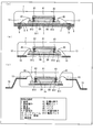
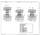
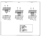
- (A)-(d) is sectional drawing which shows the mounting structure of the semiconductor device of this invention. It is sectional drawing which shows the Example of joining between the connection terminals of this invention. It is sectional drawing which shows the Example of joining between the connection terminals of this invention. It is sectional drawing which shows the Example of joining between the connection terminals of this invention. It is sectional drawing which shows the Example of joining between the connection terminals of this invention. It is sectional drawing which shows the Example of joining between the connection terminals of this invention. It is sectional drawing which shows the Example of joining between the connection terminals of this invention. It is sectional drawing which shows the Example of joining between the connection terminals of this invention. It is sectional drawing which shows the Example of joining between the connection terminals of this invention. (A)-(c) is sectional drawing which shows the modification of the mounting structure of the semiconductor device of this invention.
- FIG. 1A is a sectional view showing a mounting structure of a semiconductor device according to the present invention.
- each component has at least one connection terminal (electrode pad A3 and substrate terminal 4) on the surface thereof. is doing.
- Each component uses a plurality of connection terminals (electrode pads A3 and substrate terminals 4) included in each component to electrically join the semiconductor element A1 and the substrate 2 together.
- the electrical bonding is performed by bumps A5 and B6 made of different metals, and a resin 7 is formed so as to cover the surface side of the substrate 2.
- An external terminal 9 that is electrically connected to the electrical junction via the substrate terminal 4 and the through hole 8 is formed on the back side of the substrate 2.
- soldering since soldering is not required, the problem of soldering can be avoided. Specifically, many processes, materials, and time costs, such as solder application, flux application, reflow, and flux removal, which are required when joining using solder can be suppressed. In addition, it is possible to avoid a problem that electrical conduction cannot be obtained due to remelting of the solder joint due to heat such as a short circuit between adjacent terminals due to a solder bridge with a narrow pitch and reflow applied during assembly by the user.
- FIG. 1B is a cross-sectional view showing a mounting structure of a semiconductor device according to the present invention.
- each component has at least one connection terminal (electrode pad A3 and substrate terminal 4) on the surface thereof. ing.
- Each component uses a plurality of connection terminals (electrode pads A3 and substrate terminals 4) included in each component to electrically join the semiconductor element A1 and the substrate 2 together.
- the bumps A5 and B6 made of metals having different hardnesses are joined, and the resin 7 is formed so as to be filled between the semiconductor element A1 and the substrate 2.
- an external terminal 9 electrically connected to the electrical junction via the substrate terminal 4 and the through hole 8 is formed on the back surface side of the substrate 2.
- FIG. 1 (b) is different from FIG. 1 (a) in that the resin is coated only between the semiconductor and the substrate.
- the amount of resin used is reduced, leading to a reduction in manufacturing cost of the semiconductor device.
- FIG. 1C is a cross-sectional view showing a mounting structure of a semiconductor device according to the present invention.
- connection terminal (electrode pad A3 and lead frame (lead) 10) is provided on the surface of each component. )have.
- Each component uses a plurality of connection terminals (electrode pad A3 and lead frame (lead) 10) that each component has to electrically join the semiconductor element A1 and the lead frame 10 together.
- the electrical bonding is a semiconductor device in which a resin 7 is formed so as to cover the surface side of the lead frame 10 by bonding with bumps A5 and B6 made of metals of different hardness.
- the difference between (c) in FIG. 1 and (a) in FIG. 1 is the difference in the components.
- the lead frame 10 instead of the substrate 2 of the first embodiment, the lead frame 10 itself serves as an external terminal.
- substrate 2 in (a) of FIG. 1 become unnecessary.
- the number of manufacturing steps of the semiconductor device is reduced, leading to a reduction in manufacturing cost of the semiconductor device.
- FIG. 1D is a cross-sectional view showing a mounting structure of a semiconductor device according to the present invention.
- FIG. 1 (d) and FIG. 1 (c) are different in the form of the lead frame. Since the shape of the lead frame is not particular, the lead frame can be arranged where necessary.
- connection terminals of the present invention Furthermore, examples of joining between the connection terminals of the present invention will be described below.
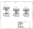
- FIG. 2A is a cross-sectional view of bonding between connection terminals according to the present invention.
- FIG. 2A is an example of bonding between the semiconductor element A1 and the semiconductor element B11 (or the substrate 2).
- a bump A5 of hard metal is formed on the electrode pad A3 of the semiconductor element A1 on the wafer after grinding with a wire bonding apparatus and a bump bonding apparatus.
- a soft metal bump B6 is formed on the electrode pad B12 (or substrate terminal 4) of the semiconductor element B11 (or substrate 2) by a plating method and a vapor deposition method. Flip chip joining each other. As a result, the bump A5 is convex and the bump B6 is concave as in the cross section of FIG.
- a capillary 34 (a wire 31 is inserted) provided in the wire bonding apparatus is used.
- the ball portion 33 is formed on the wire 31 protruding from the tip of the capillary 34 using spark discharge or the like.
- the formed ball portion 33 is pressed against the electrode pad 32a using the capillary 34 and joined to the electrode pad 32a by ultrasonic welding or the like.
- the bump 35 is formed by cutting the wire near the base of the joined ball.
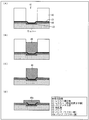
- a resist opening 41 is formed on the wafer in order to form bumps by plating.
- the resist opening 41 is formed by opening the resist 42 on a wiring terminal portion called a pad 45 connected to a circuit in the chip.
- a barrier metal layer 43 (a metal film for preventing the diffusion of bump metal and having conductivity) is formed under the resist 42, and a protective film 44 is formed under the barrier metal layer 43. Is formed. Electroplating by electrolysis is performed by energizing through the barrier metal layer 43 from the edge of the wafer [(B) of FIG. 6]. Since only the resist opening 41 is in contact with the plating solution, the bump 46 is formed following the resist opening 41.
- the wafer is transferred to the next process apparatus, and resist stripping and barrier metal etching (removing unnecessary barrier metal layers other than the bumps by etching) are performed (FIG. 6). (C)]. Thereafter, the wafer is heated in a reflow furnace to make a bump 46a from the bump 46 (FIG. 6D).
- the stud bump can be formed by forming a bump using a wire bonding apparatus, and the plated bump can be formed by forming a bump using a plating method.
- semiconductor devices are similarly required to reduce manufacturing costs.
- the following factors can be considered as a cost increase of the manufacturing method.
- the bump forming position can be individually adjusted with respect to the electrode pad and the substrate terminal. Therefore, it is possible to form bumps with high positional accuracy, and it is possible to detect the non-formation and non-attachment of bumps. Further, the same effects as described above can be obtained even when bumps are formed on a semiconductor chip divided into individual pieces from a wafer. Further, when bumps are formed on the ground wafer, the following advantages are obtained. First, since the position of the conductor element is constant, position detection is short and position correction is easy. One is short bump formation time because the semiconductor device is not individually conveyed. First, after grinding, the bump formation conditions are restricted, but if bonding is possible, the bumps will not be damaged thereafter.
- bumps when bumps are formed on an unground wafer, bumps can be formed at a high temperature because a sheet for holding a thin ground wafer is not required.
- problems such as the presence of bubbles when the protective sheet is applied to the bump forming surface, and the bump dropout when removing the sheet.
- the tip portion of the bump has a pointed shape, it can be easily embedded in the other protruding electrode and can be more reliably bonded.
- flip chip bonding that enables highly reliable electric bonding can be performed by forming bumps on a wafer after grinding at least one bump by a wire bonding apparatus and a bump bonding apparatus.
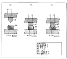
- FIG. 2B is a cross-sectional view of bonding between connection terminals according to the present invention.
- FIG. 2B is an example of bonding between the semiconductor element A1 and the semiconductor element B11 (or the substrate 2).
- a hard metal bump A5 is formed on the electrode pad A3 of the semiconductor element A1 by a wire bonding apparatus and a bump bonding apparatus.
- a soft metal bump B6 is formed on the electrode pad B12 (or substrate terminal 4) of the semiconductor element B11 (or substrate 2) by a wire bonding apparatus and a bump bonding apparatus, and they are flip-chip bonded to face each other.
- the bump A5 has a convex shape and the bump B6 has a concave shape as shown in the cross section of FIG.
- the difference from FIG. 2A is that all the bumps are formed by the wire bonding apparatus and the bump bonding apparatus.
- the following problems cost increase
- the cost is increased due to transport damage to the joints between the bumps, the electrode pads, and the substrate terminals.
- bump formation is performed by outsourcing, bumps are formed on all semiconductor elements in the wafer, so that the cost of bumps formed on defective semiconductor elements is added to non-defective semiconductor elements. Cost is up.
- bumps are formed on the wafer instead of individually, when the position shift occurs due to some manufacturing abnormality, the cost increases when the position shift occurs in the entire wafer. .
- this is an increase in cost when introducing inspections for detecting these.
- the problems (cost increase) due to the bump formation in the above plating method and vapor deposition method can be avoided by performing all the above bump formation with a wire bonding apparatus and a bump bonding apparatus.
- FIG. 2C is a cross-sectional view of bonding between connection terminals according to the present invention.
- FIG. 2C shows an example of bonding between the semiconductor element A1 and the semiconductor element B11 (or the substrate 2).
- the difference from FIG. 2B is that leveling is performed on the soft bump B6 in FIG. 2B to form a flat portion facing the bump A5.
- FIG. 2D is a cross-sectional view of bonding between connection terminals according to the present invention.
- FIG. 2D is an example of bonding between the semiconductor element A1 and the semiconductor element B11 (or the substrate 2).
- a hard metal bump A5 is formed on the electrode pad A3 of the semiconductor element A1 by a wire bonding apparatus and a bump bonding apparatus.
- a hard metal bump A5 is also formed on the electrode pad B12 (or substrate terminal 4) of the semiconductor element B11 (or substrate 2) by a wire bonding apparatus and a bump bonding apparatus.
- a soft metal bump B6 is formed on the bump A5 on the electrode pad B12 (or the substrate terminal 4). Flip chip joining each other. As a result, the bump A5 is convex and the bump B6 is concave as in the cross section of FIG. 2D (c).
- a hard metal bump A5 is applied to both the electrode pad A3 of the semiconductor element A1 and the electrode pad B12 (or the substrate terminal 4 of the substrate 2) of the semiconductor element B11 located opposite thereto.
- a bump bonding apparatus A soft metal bump B6 is formed on the bump A5 on the opposing electrode pad B12 (or the substrate terminal 4 of the substrate 2) to perform flip chip bonding.
- FIG. 2E is a cross-sectional view of bonding between connection terminals according to the present invention.
- FIG. 2E shows an example of bonding between the semiconductor element A1 and the semiconductor element B11 (or the substrate 2).
- leveling is performed on the soft bump B6 of FIG. 2D to form a flat portion facing the bump A5 on the electrode pad A3 of the semiconductor element A1.
- FIG. 2F is a cross-sectional view of the connection between the connection terminals according to the present invention.
- FIG. 2F is an example of bonding between the semiconductor element A1 and the semiconductor element B11 (or the substrate 2).
- a hard metal bump A5 is formed on the electrode pad A3 of the semiconductor element A1 by a wire bonding apparatus and a bump bonding apparatus.
- the electrode pad B12 (or substrate terminal 4) of the semiconductor element B11 (or substrate 2) has a thickness corresponding to the soft metal bump B6. Flip chip joining each other. As a result, the bump A5 is convex and the electrode pad B12 (or the substrate terminal 4) is concave as in the cross section of FIG. 2F (c).
- the electrode pads of the semiconductor elements located opposite to each other or the substrate terminals 4 of the substrate 2 have a thickness corresponding to the soft metal bumps B6, and the bumps and the electrode pads or the substrate terminals of the substrate 2 This is the point where 4 is directly joined.
- FIG. 2G is a cross-sectional view of bonding between connection terminals according to the present invention.
- FIG. 2G is an example of joining of the semiconductor element A1 and the lead frame 10.
- a hard metal bump A5 is formed on the electrode pad A3 of the semiconductor element A1 by a wire bonding apparatus and a bump bonding apparatus.
- a soft metal bump B6 is formed on the lead frame 10 by a plating method and a vapor deposition method. Flip chip joining each other.
- the bump A5 is convex and the bump B6 is concave as in the cross section of FIG.
- the constituent elements are the semiconductor element A 1 and the lead frame 10.
- the hard metal bump A5, the soft metal bump B6, and the upper and lower configurations are not limited to the above embodiment.
- the metal structure of the bump is preferably a structure using gold, silver, or copper, and these metals are well-known facts that have good compatibility with each other and are available as general materials. It is a material that is easy to use and has a long history of use. Furthermore, a desirable configuration using these metals is to form one with copper. This is because the material cost is low and it is the hardest characteristic among them. The other is generally used in joining semiconductor devices, and it is desirable to use gold which is the softest of these. Also, if the cost is lower than gold or the environment such as anti-oxidation required for using copper is not prepared, the hardness differs by selecting silver that is harder than gold and softer than copper. Bump configuration can be joined.
- a copper wire metal-coated with palladium or the like is used, and the bump is formed in an environment using an inert gas.
- the bump surface is prevented from being oxidized, process management and material management are facilitated, and reliability in bonding is also increased. Further, the bonding reliability can be improved by performing a plasma treatment or the like to clean and activate the bump surface.
- FIG. 3A is a sectional view showing a modification of the mounting structure of the semiconductor device according to the present invention.
- 3A includes three components (semiconductor element A1, semiconductor element B11, and substrate 2), and at least one connection terminal (electrode pad A3 and electrode pad B12) is provided on the surface of each component. And substrate terminal 4).
- the semiconductor element A1 and the semiconductor element B11 are electrically joined by using a plurality of connection terminals (electrode pad A3 and electrode pad B12) each has.
- the bumps A5 and B6 made of metals having different hardnesses are joined.
- the substrate 2 and the semiconductor element B11 are electrically joined. This electrical connection is performed by wire wiring 13.
- the resin 7 is formed so as to cover the front surface side of the substrate 2, and the external terminal 9 electrically connected to the semiconductor element B 11 through the wire wiring 13, the substrate terminal 4 and the through hole 8 is connected to the back surface of the substrate 2.
- This is a semiconductor device formed on the side.
- the difference from (a) in FIG. 1 is that there are three components.
- the bonding of the wire wiring 13 and electrically bonding the three components of the semiconductor element A1, the semiconductor element B11, and the substrate 2 it is possible to deal with more complicated circuits and reduce the circuit area.
- FIG. 3B is a cross-sectional view showing a modification of the mounting structure of the semiconductor device according to the present invention.
- 3B includes three components (semiconductor element A1, semiconductor element B11, and lead frame 10), and at least one connection terminal (electrode pad A3 and electrode pad) is provided on the surface of each component. B12 and lead frame 10).
- connection terminals electrode pad A3 and electrode pad B12
- each has the semiconductor element A1 and the semiconductor element B11 fixed to the reinforcing plate 14 are electrically joined.
- the bumps A5 and B6 made of metals having different hardnesses are joined.
- the semiconductor element B11 fixed to the reinforcing plate 14 and the lead frame 10 are electrically joined. This electrical bonding is performed by wire wiring 13.
- the semiconductor device is formed with a resin 7 so as to cover the surface side of the lead frame 10.
- a lead frame 10 is used in place of the substrate 2 in FIG. Although the reinforcing plate 14 is required, since the lead frame 10 itself serves as an external terminal, a through-hole and an external terminal that are necessary for attaching the external terminal to the substrate are not necessary, and the number of processes is reduced. Decrease, leading to cost reduction.
- FIG. 3C is a cross-sectional view showing a modification of the mounting structure of the semiconductor device according to the present invention.
- FIG. 3 (c) and FIG. 3 (b) are different in the form of the lead frame of the second modification of the above embodiment. Since the shape of the lead frame is not particular, the lead frame can be arranged where necessary.
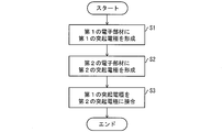
- FIG. 7 is a flowchart showing the process.
- a first protruding electrode is formed on a first electronic member (step S1). At this time, the first protruding electrode is formed using a wire bonding apparatus and a bump bonding apparatus.
- a second protruding electrode is formed on the second electronic member (step S2).
- the second protruding electrode is formed by using a wire bonding apparatus and a bump bonding apparatus, or a plating method and a vapor deposition method.
- the first protruding electrode is embedded (bonded) in the second protruding electrode (step S3).
- a load is applied and crimped.
- metal can be joined by thermocompression by applying heat.
- the first electronic component indicates a substrate or a semiconductor element mounted on the substrate
- the second electronic component indicates a semiconductor element. Further, it is desirable to use copper for the first protruding electrode and gold for the second protruding electrode.
- connection terminals For reference, an embodiment of joining between connection terminals in the prior art will be described below.
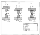
- FIG. 4A is a cross-sectional view of joining between connection terminals according to the prior art.
- FIG. 4A shows an example of bonding between the semiconductor element A1 and the semiconductor element B11 (or the substrate 2).
- a post 15 is formed on the electrode pad A3 of the semiconductor element A1, and solder 16 is applied to the tip of the post 15.
- a metal layer or bump B6 is formed on the electrode pad B12 (or substrate terminal 4) of the semiconductor element B11 (or substrate 2) by a plating method and a vapor deposition method, and a flux 17 is applied to the surface.
- Each of them is flip-chip mounted face-to-face, the solder 16 is melted by reflow, and the post 15 and the metal layer or bump B6 are solder-melt bonded.
- the post 15 and the metal layer or bump B6 sandwich the solder 16 as shown in the cross section of FIG.
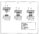
- FIG. 4B is a cross-sectional view of joining between connection terminals according to the prior art.
- FIG. 4B is an example of bonding between the semiconductor element A1 and the semiconductor element B11 (or the substrate 2).
- a post 15 is formed on the electrode pad A3 of the semiconductor element A1 and on the electrode pad B12 (or substrate terminal 4) of the semiconductor element B11 (or substrate 2), and solder 16 is applied to the tip of the post 15.
- the flux 17 is applied to the surface of the semiconductor element B11 (or the substrate 2), each of them is face-to-face flip-chip mounted, the solder 16 is melted by reflow, and the posts 15 are solder-bonded. As a result, the solder 16 is sandwiched between the posts 15 as shown in the cross section of FIG. 4B (c).
- FIG. 4C is a cross-sectional view of joining between connection terminals according to the prior art.
- FIG. 4C shows an example of bonding between the semiconductor element A1 and the semiconductor element B11 (or the substrate 2).
- a bump A5 is formed on the electrode pad A3 of the semiconductor element A1 by a wire bonding apparatus and a bump bonding apparatus, and solder (solder bump) 16 is formed on the electrode pad B12 (or substrate terminal 4) of the semiconductor element B11 (or substrate 2).
- Flux 17 is applied to the surface of the semiconductor element B11 (or substrate 2), each of them is face-to-face flip-chip mounted, solder (solder bump) 16 is melted by reflow, and the bump A5 and electrode pad B12 (or substrate terminal) 4) and solder fusion bonding.
- the bump A5 has a convex shape and the solder (solder bump) 16 has a concave shape as shown in FIG.
- solder is used for joining.
- many processes and materials such as solder application on bumps and posts, flux application, reflow, and flux removal are required, which takes time and cost.
- electrical conduction cannot be obtained due to remelting of the solder joint due to heat such as a short circuit between adjacent terminals due to a narrow pitch solder bridge or reflow applied during assembly by the user.
- FIG. 4D is a cross-sectional view of bonding between connection terminals according to the prior art.
- FIG. 4D shows an example of bonding between the semiconductor element A1 and the semiconductor element B11 (or the substrate 2).
- a bump A5 is formed on the electrode pad A3 of the semiconductor element A1 by a wire bonding apparatus and a bump bonding apparatus.
- Flip chip mounting is carried out on the electrode pad B12 (or substrate terminal 4) of the semiconductor element B11 (or substrate 2) facing each other, and the bump A5 and the electrode pad B12 (or substrate terminal 4) are bonded by ultrasonic thermocompression bonding. Join metal.
- the bump A5 and the electrode pad B12 (or the substrate terminal 4) are fused as shown in the cross section of FIG.
- the main difference from the present invention is that ultrasonic waves are used for bonding.
- ultrasonic waves are used for bonding, there is a concern that damage such as a change in the shape of the bump or peeling due to the amplitude of the ultrasonic waves may occur.
- a semiconductor device includes a first electronic component having a first protruding electrode and a second protruding electrode connected to the first protruding electrode.
- the first protruding electrode and the second protruding electrode are made of different metal materials, and the first protruding electrode is harder than the second protruding electrode, and the first protruding electrode The tip of the protruding electrode on the second protruding electrode side is embedded in the second protruding electrode.
- the hardness of the metal is different, the first protruding electrode is embedded in the second protruding electrode, and the first protruding electrode and the second protruding electrode
- the interface in the junction cross-section with the protruding electrode is uneven. Due to the unevenness of the joint surfaces, friction due to sliding occurs at the interface between the protruding electrodes, and the new surface is easily exposed. Therefore, the joining which does not use the ultrasonic wave used for exposing the new surface is possible, and the problem of joining by the ultrasonic wave can be avoided. Specifically, it is possible to avoid damage such as a change in the shape of the bump or peeling due to the amplitude of the ultrasonic wave, which is considered when bonding is performed using ultrasonic waves.
- the first protruding electrode and the second protruding electrode are directly joined.
- the problem of joining by solder can be avoided. Specifically, many processes, materials, time, and costs, such as solder application, flux application, reflow, and flux removal, which are required when joining using solder can be suppressed. In addition, it is possible to avoid a problem that electrical conduction cannot be obtained due to remelting of the solder joint due to heat such as a short circuit between adjacent terminals due to a solder bridge with a narrow pitch and reflow applied during assembly by the user.
- the tip portion of the first protruding electrode has a pointed shape.
- the tip portion of the first protruding electrode since the tip portion of the first protruding electrode has a pointed shape, it can be easily embedded in the second protruding electrode as compared with the rounded tip shape, and can be more reliably joined. Can do.
- the first protruding electrode is a stud bump.
- the first protruding electrode is a stud bump
- a sharply shaped bump can be formed, and it can be easily embedded in the second protruding electrode and can be more reliably bonded.
- bumps can be directly formed on the electrode pads individually for each semiconductor element, and the bump formation position can be determined and corrected only by position information. As a result, bumps can be formed only on non-defective products among the semiconductor elements installed in the wafer, and an increase in cost that occurs when formed on defective products can be prevented. Further, it can be formed on the same production line as that for flip chip bonding, and transport damage can be avoided.
- the first protruding electrode is copper
- a copper wire that is metal-coated with palladium or the like and performing bump formation in an environment using an inert gas oxidation of copper can be suppressed, process control and Material management becomes easy, flip chip bonding is possible in a fresher state, and bonding reliability is increased.
- the second protruding electrode is a stud bump or a plated bump.
- the second protruding electrode is a plated bump
- batch bump formation is possible on a wafer basis, and the bump can be formed in the shortest time, thereby reducing the time.
- the soft metal bump since flat bumps can be easily formed, when a hard metal bump is pressed against a soft metal bump, the soft metal bump has a wider and flat surface, so that the positional deviation during flip chip bonding is reduced. Even when this occurs, the cross-sectional shape tends to be uneven, and a stable joint state can be secured.
- the length of the second protruding electrode is equal to the first protrusion. It is preferable that it is larger than the length of the said front-end
- the first bump electrode and the second bump electrode positioned opposite to each other are directly bonded to each other, so that the step of forming the bump positioned opposite to the first bump electrode can be omitted. Therefore, the process can be shortened, leading to cost reduction.
- the first electronic component is a substrate or a semiconductor element mounted on the substrate
- the first protruding electrode is a copper bump
- the second electronic component Is a semiconductor element
- the second protruding electrode is preferably a gold bump.
- copper and gold are metals that have good compatibility with each other in crimp bonding, are easily available as general materials, have a good track record of use, and have high reliability in connection use.
- a desirable configuration using copper and gold one is formed as a hard copper bump of copper as described above, and the other is formed as a soft bump of gold. This makes it possible to form metal bumps with high reliability and low material costs in joining semiconductor devices.
- heat is applied in the bonding, if heat is applied to the substrate made of resin, gas or reactant may be generated. Therefore, heat is applied not to the substrate but to the semiconductor element. By forming copper bumps on the substrate side where no heat is applied, copper oxidation can be prevented.
- the first protruding electrode is partially covered with a metal material different from the metal material constituting the first protruding electrode.
- the copper bump formation of the first protruding electrode is performed in an environment using an inert gas using a copper wire that is metal-coated with a different metal (a metal that is difficult to oxidize) (eg, palladium).
- a different metal eg, palladium
- the second protruding electrode has a structure in which two kinds of metal materials are stacked.
- the first electronic component and the second electronic component are joined using the three bumps.
- a method of manufacturing a semiconductor device is a method of manufacturing the semiconductor device, wherein the first protruding electrode is formed of copper on the first electronic component by a bonding apparatus using a wire; Forming the second protruding electrode with gold by a bonding apparatus using a wire or a plating method on the second electronic component, and applying the heat to the second electronic component, the first protruding electrode Embedded in the second protruding electrode.
- the first protruding electrode formed on the first electronic component and the second protruding electrode formed on the second electronic component are directly joined without using solder, ultrasonic waves, or the like.
- a semiconductor device can be manufactured.
- At least one of the first electronic component and the second electronic component is a semiconductor element, and the first or second protruding electrode on the semiconductor element. Is preferably performed on a semiconductor chip divided into individual pieces from a wafer.
- the bump forming position can be individually adjusted with respect to the electrode pad and the substrate terminal. Accordingly, bumps with high positional accuracy can be formed. Furthermore, when forming in the form of a wafer, the following problems can be considered. If it is before grinding, the bumps are damaged during grinding and when the surface protection sheet after grinding is peeled off. After grinding, a protective sheet for holding a thin wafer is interposed between the chip and the stage, so that there is a restriction in bump formation. Further, in common before and after grinding, there is a restriction when mounting a semiconductor element on a substrate or a reinforcing plate of a semiconductor device formed with three components. Therefore, the above problem can be avoided by forming the bumps on the semiconductor chips divided into individual pieces from the wafer instead of forming the bumps in the form of a wafer as in the above manufacturing method.
- the step of forming the first protruding electrode is preferably performed in an environment filled with an inert gas.
- the bump surface is prevented from being oxidized, process management and material management are facilitated, and a semiconductor device having high reliability in bonding can be manufactured.
- the surfaces of the first and second protruding electrodes are It is preferable to clean.
- the above manufacturing method by performing cleaning using plasma processing or the like, the surfaces of the first and second protruding electrodes are cleaned and activated, and a semiconductor device with high bonding reliability can be manufactured.
- the present invention can be used for a semiconductor device using a flip chip technique and a manufacturing method thereof.
Landscapes
- Wire Bonding (AREA)
- Engineering & Computer Science (AREA)
- Manufacturing & Machinery (AREA)
Abstract
Description
第1の突起電極を有する第1の電子部品と、
上記第1の突起電極と接続された第2の突起電極を有する第2の電子部品とを備え、
上記第1の突起電極と上記第2の突起電極とは、互いに異なる金属材料からなり、
上記第1の突起電極は、上記第2の突起電極より硬く、
上記第1の突起電極の上記第2の突起電極側の先端部分が上記第2の突起電極に埋め込まれていることを特徴とする。
図1の(a)に基づき、本発明の一実施形態である半導体装置の実装構造について説明する。
図1の(b)に基づき、本発明の実施形態である半導体装置の別の実装構造について説明する。
図1の(c)に基づき、本発明の実施形態である半導体装置の別の実装構造について説明する。
図1の(d)に基づき、本発明の実施形態である半導体装置の別の実装構造について説明する。
図2Aに基づき、本発明の実施形態に係る接続端子間の接合について説明する。
図2Bに基づき、本発明の実施形態に係る接続端子間の接合について説明する。
図2Cに基づき、本発明の実施形態に係る接続端子間の接合について説明する。
図2Dに基づき、本発明の実施形態に係る接続端子間の接合について説明する。
図2Eに基づき、本発明の実施形態に係る接続端子間の接合について説明する。
図2Fに基づき、本発明の実施形態に係る接続端子間の接合について説明する。
図2Gに基づき、本発明の実施形態に係る接続端子間の接合について説明する。
図3の(a)に基づき、本発明の半導体装置の実装構造の実施形態の変形について説明する。
図3の(b)に基づき、本発明の半導体装置の実装構造の実施形態の変形について説明する。
図3の(c)に基づき、本発明の半導体装置の実装構造の実施形態の変形について説明する。
次に、図7に基づき、半導体装置の製造方法について説明する。図7はその工程を示すフローチャートである。
図4Aに基づき、従来技術の接続端子間の接合について説明する。
図4Bに基づき、従来技術の接続端子間の接合について説明する。
図4Cに基づき、従来技術の接続端子間の接合について説明する。
図4Dに基づき、従来技術の接続端子間の接合について説明する。
2 基板
A3 電極パッド
4 基板端子
A5 バンプ
B6 バンプ
7 樹脂
8 貫通孔
9 外部端子
10 リードフレーム
B11 半導体素子
B12 電極パッド
13 ワイヤー配線
14 補強板
15 ポスト
16 半田
17 フラックス
31 ワイヤー
32a 電極パッド
33 ボール部
34 キャピラリー
35 バンプ
41 レジスト開口部
42 レジスト(感光性高分子膜)
43 バリアメタル層
44 保護膜
45 パッド
46 バンプ(リフロー前)
46a バンプ(リフロー後)
Claims (13)
- 第1の突起電極を有する第1の電子部品と、
上記第1の突起電極と接続された第2の突起電極を有する第2の電子部品と
を備え、
上記第1の突起電極と上記第2の突起電極とは、互いに異なる金属材料からなり、
上記第1の突起電極は、上記第2の突起電極より硬く、
上記第1の突起電極の上記第2の突起電極側の先端部分が上記第2の突起電極に埋め込まれていることを特徴とする半導体装置。 - 上記第1の突起電極と上記第2の突起電極は、直接的に接合していることを特徴とする請求項1に記載の半導体装置。
- 上記第1の突起電極の上記先端部分は、尖頭形状を有することを特徴とする請求項1または2に記載の半導体装置。
- 上記第1の突起電極は、スタッドバンプであることを特徴とする請求項1から3のいずれか1項に記載の半導体装置。
- 上記第2の突起電極は、スタッドバンプまたはメッキバンプであることを特徴とする請求項1から4のいずれか1項に記載の半導体装置。
- 上記第1の突起電極の上記先端部分が上記第2の突起電極に埋め込まれた方向において、上記第2の突起電極の長さは、上記第1の突起電極の上記先端部分の長さよりも大きいことを特徴とする請求項1から5のいずれか1項に記載の半導体装置。
- 上記第1の電子部品は、基板または基板上に搭載された半導体素子であり、
上記第1の突起電極は、銅バンプであり、
上記第2の電子部品は、半導体素子であり、
上記第2の突起電極は、金バンプあることを特徴とする請求項1から6のいずれか1項に記載の半導体装置。 - 上記第1の突起電極は、自身を構成する金属材料とは異なる金属材料で部分的に被覆されていることを特徴とする請求項7に記載の半導体装置。
- 上記第2の突起電極は、2種類の金属材料を積み重ねた構造を有することを特徴とする請求項1から8のいずれか1項に記載の半導体装置。
- 請求項1に記載の半導体装置の製造方法であって、
上記第1の電子部品に、ワイヤーを用いたボンディング装置によって上記第1の突起電極を銅で形成する工程と、
上記第2の電子部品に、ワイヤーを用いたボンディング装置またはメッキ工法によって上記第2の突起電極を金で形成する工程と、
上記第2の電子部品に熱を加えながら、上記第1の突起電極の上記先端部分を上記第2の突起電極に埋め込む工程とを含むことを特徴とする半導体装置の製造方法。 - 上記第1の電子部品および上記第2の電子部品の少なくとも一方は、半導体素子であり、
上記半導体素子への上記第1または第2の突起電極の形成は、ウェハーから個片に分割された半導体チップに対して行なわれることを特徴とする請求項10に記載の半導体装置の製造方法。 - 上記第1の突起電極を形成する工程は、不活性ガスが充填された環境において行なわれることを特徴とする請求項10または11に記載の半導体装置の製造方法。
- 上記第1の突起電極の上記先端部分を上記第2の突起電極に埋め込む工程の前処理として、上記第1および第2の突起電極の表面を洗浄化することを特徴とする請求項10から12のいずれか1項に記載の半導体装置の製造方法。
Priority Applications (3)
| Application Number | Priority Date | Filing Date | Title |
|---|---|---|---|
| JP2014529471A JPWO2014024796A1 (ja) | 2012-08-08 | 2013-08-02 | 半導体装置およびその製造方法 |
| US14/420,049 US20150200176A1 (en) | 2012-08-08 | 2013-08-02 | Semiconductor device and method for producing same |
| CN201380041465.5A CN104541366A (zh) | 2012-08-08 | 2013-08-02 | 半导体装置及其制造方法 |
Applications Claiming Priority (2)
| Application Number | Priority Date | Filing Date | Title |
|---|---|---|---|
| JP2012-176417 | 2012-08-08 | ||
| JP2012176417 | 2012-08-08 |
Publications (1)
| Publication Number | Publication Date |
|---|---|
| WO2014024796A1 true WO2014024796A1 (ja) | 2014-02-13 |
Family
ID=50068025
Family Applications (1)
| Application Number | Title | Priority Date | Filing Date |
|---|---|---|---|
| PCT/JP2013/071005 Ceased WO2014024796A1 (ja) | 2012-08-08 | 2013-08-02 | 半導体装置およびその製造方法 |
Country Status (5)
| Country | Link |
|---|---|
| US (1) | US20150200176A1 (ja) |
| JP (1) | JPWO2014024796A1 (ja) |
| CN (1) | CN104541366A (ja) |
| TW (1) | TW201411793A (ja) |
| WO (1) | WO2014024796A1 (ja) |
Cited By (3)
| Publication number | Priority date | Publication date | Assignee | Title |
|---|---|---|---|---|
| WO2016143687A1 (ja) * | 2015-03-06 | 2016-09-15 | 三菱重工業株式会社 | 接合方法、および、接合体 |
| KR20170005774A (ko) * | 2014-12-29 | 2017-01-16 | 스태츠 칩팩 피티이. 엘티디. | 인터포저 지지 구조 메커니즘을 갖는 집적 회로 패키징 시스템 및 그 제조 방법 |
| EP3163609B1 (en) * | 2014-07-29 | 2024-09-11 | Huawei Technologies Co., Ltd. | Chip integration method |
Families Citing this family (2)
| Publication number | Priority date | Publication date | Assignee | Title |
|---|---|---|---|---|
| JP6215755B2 (ja) * | 2014-04-14 | 2017-10-18 | ルネサスエレクトロニクス株式会社 | 半導体装置 |
| DE112016002608T5 (de) * | 2015-06-11 | 2018-03-08 | Mitsubishi Electric Corporation | Verfahren zur Herstellung einer Leistungs-Halbleitervorrichtung und Leistungs-Halbleitervorrichtung |
Citations (2)
| Publication number | Priority date | Publication date | Assignee | Title |
|---|---|---|---|---|
| JPH08213425A (ja) * | 1995-02-03 | 1996-08-20 | Matsushita Electron Corp | 半導体装置およびその製造方法 |
| JP2000216198A (ja) * | 1999-01-26 | 2000-08-04 | Matsushita Electric Ind Co Ltd | 半導体装置およびその製造方法 |
Family Cites Families (5)
| Publication number | Priority date | Publication date | Assignee | Title |
|---|---|---|---|---|
| US5046657A (en) * | 1988-02-09 | 1991-09-10 | National Semiconductor Corporation | Tape automated bonding of bumped tape on bumped die |
| US20030001286A1 (en) * | 2000-01-28 | 2003-01-02 | Ryoichi Kajiwara | Semiconductor package and flip chip bonding method therein |
| JP3778276B2 (ja) * | 2002-01-21 | 2006-05-24 | セイコーエプソン株式会社 | 半導体装置の製造方法 |
| JP2005174981A (ja) * | 2003-12-08 | 2005-06-30 | Olympus Corp | 電子部品の製造方法及び電子部品 |
| JP2008277647A (ja) * | 2007-05-02 | 2008-11-13 | Epson Imaging Devices Corp | 実装構造体及び電子機器 |
-
2013
- 2013-08-02 JP JP2014529471A patent/JPWO2014024796A1/ja active Pending
- 2013-08-02 US US14/420,049 patent/US20150200176A1/en not_active Abandoned
- 2013-08-02 CN CN201380041465.5A patent/CN104541366A/zh active Pending
- 2013-08-02 WO PCT/JP2013/071005 patent/WO2014024796A1/ja not_active Ceased
- 2013-08-07 TW TW102128377A patent/TW201411793A/zh unknown
Patent Citations (2)
| Publication number | Priority date | Publication date | Assignee | Title |
|---|---|---|---|---|
| JPH08213425A (ja) * | 1995-02-03 | 1996-08-20 | Matsushita Electron Corp | 半導体装置およびその製造方法 |
| JP2000216198A (ja) * | 1999-01-26 | 2000-08-04 | Matsushita Electric Ind Co Ltd | 半導体装置およびその製造方法 |
Cited By (4)
| Publication number | Priority date | Publication date | Assignee | Title |
|---|---|---|---|---|
| EP3163609B1 (en) * | 2014-07-29 | 2024-09-11 | Huawei Technologies Co., Ltd. | Chip integration method |
| KR20170005774A (ko) * | 2014-12-29 | 2017-01-16 | 스태츠 칩팩 피티이. 엘티디. | 인터포저 지지 구조 메커니즘을 갖는 집적 회로 패키징 시스템 및 그 제조 방법 |
| KR102561718B1 (ko) | 2014-12-29 | 2023-07-31 | 스태츠 칩팩 피티이. 엘티디. | 인터포저 지지 구조 메커니즘을 갖는 집적 회로 패키징 시스템 및 그 제조 방법 |
| WO2016143687A1 (ja) * | 2015-03-06 | 2016-09-15 | 三菱重工業株式会社 | 接合方法、および、接合体 |
Also Published As
| Publication number | Publication date |
|---|---|
| CN104541366A (zh) | 2015-04-22 |
| JPWO2014024796A1 (ja) | 2016-07-25 |
| TW201411793A (zh) | 2014-03-16 |
| US20150200176A1 (en) | 2015-07-16 |
Similar Documents
| Publication | Publication Date | Title |
|---|---|---|
| KR100531393B1 (ko) | 반도체 장치 및 그 제조 방법 | |
| KR101594220B1 (ko) | 전자 부품, 전자 장치의 제조 방법 및 전자 장치 | |
| TWI493672B (zh) | 半導體裝置、電子裝置及半導體裝置之製造方法 | |
| KR20030051159A (ko) | 반도체장치 | |
| US20100207279A1 (en) | Semiconductor package with ribbon with metal layers | |
| WO2014024796A1 (ja) | 半導体装置およびその製造方法 | |
| US20190254164A1 (en) | Circuit board, method of manufacturing circuit board, and electronic device | |
| JP5919641B2 (ja) | 半導体装置およびその製造方法並びに電子装置 | |
| JP5113793B2 (ja) | 半導体装置およびその製造方法 | |
| CN101211885A (zh) | 钎焊接合部、电子部件、半导体器件和电子部件的制造方法 | |
| JP2010123676A (ja) | 半導体装置の製造方法、半導体装置 | |
| JP4759041B2 (ja) | 電子部品内蔵型多層基板 | |
| JP2001060760A (ja) | 回路電極およびその形成方法 | |
| JP3279470B2 (ja) | 半導体装置およびその製造方法 | |
| JP2005123463A (ja) | 半導体装置及びその製造方法、半導体装置モジュール、回路基板並びに電子機器 | |
| TWI605740B (zh) | 基體之接合方法 | |
| US20080212301A1 (en) | Electronic part mounting board and method of mounting the same | |
| US7944051B2 (en) | Semiconductor device having external connection terminals and method of manufacturing the same | |
| TWI527177B (zh) | 晶片構件與晶片封裝體 | |
| JP2020031081A (ja) | 半導体装置 | |
| US20100148364A1 (en) | Semiconductor device and method for producing semiconductor device | |
| KR101156183B1 (ko) | 범프 간 직접 접합방법 및 이를 이용한 반도체 패키지 | |
| JP6379650B2 (ja) | 半導体装置の製造方法 | |
| KR20150062544A (ko) | 인쇄회로기판 및 이를 포함하는 칩 패키지 | |
| JP2014110355A (ja) | 半導体装置 |
Legal Events
| Date | Code | Title | Description |
|---|---|---|---|
| 121 | Ep: the epo has been informed by wipo that ep was designated in this application |
Ref document number: 13828321 Country of ref document: EP Kind code of ref document: A1 |
|
| ENP | Entry into the national phase |
Ref document number: 2014529471 Country of ref document: JP Kind code of ref document: A |
|
| WWE | Wipo information: entry into national phase |
Ref document number: 14420049 Country of ref document: US |
|
| NENP | Non-entry into the national phase |
Ref country code: DE |
|
| 122 | Ep: pct application non-entry in european phase |
Ref document number: 13828321 Country of ref document: EP Kind code of ref document: A1 |