WO2014024623A1 - 密着イメージセンサ、密着イメージセンサ用出力補正装置及び密着イメージセンサ用出力補正方法 - Google Patents
密着イメージセンサ、密着イメージセンサ用出力補正装置及び密着イメージセンサ用出力補正方法 Download PDFInfo
- Publication number
- WO2014024623A1 WO2014024623A1 PCT/JP2013/068833 JP2013068833W WO2014024623A1 WO 2014024623 A1 WO2014024623 A1 WO 2014024623A1 JP 2013068833 W JP2013068833 W JP 2013068833W WO 2014024623 A1 WO2014024623 A1 WO 2014024623A1
- Authority
- WO
- WIPO (PCT)
- Prior art keywords
- light
- unit
- correction
- image sensor
- reference data
- Prior art date
- Legal status (The legal status is an assumption and is not a legal conclusion. Google has not performed a legal analysis and makes no representation as to the accuracy of the status listed.)
- Ceased
Links
Images







Classifications
-
- H—ELECTRICITY
- H04—ELECTRIC COMMUNICATION TECHNIQUE
- H04N—PICTORIAL COMMUNICATION, e.g. TELEVISION
- H04N1/00—Scanning, transmission or reproduction of documents or the like, e.g. facsimile transmission; Details thereof
- H04N1/40—Picture signal circuits
- H04N1/401—Compensating positionally unequal response of the pick-up or reproducing head
-
- H—ELECTRICITY
- H04—ELECTRIC COMMUNICATION TECHNIQUE
- H04N—PICTORIAL COMMUNICATION, e.g. TELEVISION
- H04N1/00—Scanning, transmission or reproduction of documents or the like, e.g. facsimile transmission; Details thereof
- H04N1/024—Details of scanning heads ; Means for illuminating the original
- H04N1/028—Details of scanning heads ; Means for illuminating the original for picture information pick-up
- H04N1/02815—Means for illuminating the original, not specific to a particular type of pick-up head
- H04N1/0282—Using a single or a few point light sources, e.g. a laser diode
- H04N1/02835—Using a single or a few point light sources, e.g. a laser diode in combination with a light guide, e.g. optical fibre, glass plate
-
- H—ELECTRICITY
- H04—ELECTRIC COMMUNICATION TECHNIQUE
- H04N—PICTORIAL COMMUNICATION, e.g. TELEVISION
- H04N1/00—Scanning, transmission or reproduction of documents or the like, e.g. facsimile transmission; Details thereof
- H04N1/024—Details of scanning heads ; Means for illuminating the original
- H04N1/028—Details of scanning heads ; Means for illuminating the original for picture information pick-up
- H04N1/02815—Means for illuminating the original, not specific to a particular type of pick-up head
- H04N1/0288—Means for illuminating the original, not specific to a particular type of pick-up head using a two-dimensional light source, e.g. two-dimensional LED array
-
- H—ELECTRICITY
- H04—ELECTRIC COMMUNICATION TECHNIQUE
- H04N—PICTORIAL COMMUNICATION, e.g. TELEVISION
- H04N1/00—Scanning, transmission or reproduction of documents or the like, e.g. facsimile transmission; Details thereof
- H04N1/024—Details of scanning heads ; Means for illuminating the original
- H04N1/028—Details of scanning heads ; Means for illuminating the original for picture information pick-up
- H04N1/02815—Means for illuminating the original, not specific to a particular type of pick-up head
- H04N1/02885—Means for compensating spatially uneven illumination, e.g. an aperture arrangement
-
- H—ELECTRICITY
- H04—ELECTRIC COMMUNICATION TECHNIQUE
- H04N—PICTORIAL COMMUNICATION, e.g. TELEVISION
- H04N1/00—Scanning, transmission or reproduction of documents or the like, e.g. facsimile transmission; Details thereof
- H04N1/024—Details of scanning heads ; Means for illuminating the original
- H04N1/028—Details of scanning heads ; Means for illuminating the original for picture information pick-up
- H04N1/02815—Means for illuminating the original, not specific to a particular type of pick-up head
- H04N1/02895—Additional elements in the illumination means or cooperating with the illumination means, e.g. filters
-
- H—ELECTRICITY
- H04—ELECTRIC COMMUNICATION TECHNIQUE
- H04N—PICTORIAL COMMUNICATION, e.g. TELEVISION
- H04N1/00—Scanning, transmission or reproduction of documents or the like, e.g. facsimile transmission; Details thereof
- H04N1/024—Details of scanning heads ; Means for illuminating the original
- H04N1/028—Details of scanning heads ; Means for illuminating the original for picture information pick-up
- H04N1/03—Details of scanning heads ; Means for illuminating the original for picture information pick-up with photodetectors arranged in a substantially linear array
- H04N1/031—Details of scanning heads ; Means for illuminating the original for picture information pick-up with photodetectors arranged in a substantially linear array the photodetectors having a one-to-one and optically positive correspondence with the scanned picture elements, e.g. linear contact sensors
- H04N1/0318—Integral pick-up heads, i.e. self-contained heads whose basic elements are a light-source, a lens array and a photodetector array which are supported by a single-piece frame
-
- H—ELECTRICITY
- H04—ELECTRIC COMMUNICATION TECHNIQUE
- H04N—PICTORIAL COMMUNICATION, e.g. TELEVISION
- H04N1/00—Scanning, transmission or reproduction of documents or the like, e.g. facsimile transmission; Details thereof
- H04N1/40—Picture signal circuits
- H04N1/40056—Circuits for driving or energising particular reading heads or original illumination means
-
- H—ELECTRICITY
- H04—ELECTRIC COMMUNICATION TECHNIQUE
- H04N—PICTORIAL COMMUNICATION, e.g. TELEVISION
- H04N2201/00—Indexing scheme relating to scanning, transmission or reproduction of documents or the like, and to details thereof
- H04N2201/024—Indexing scheme relating to scanning, transmission or reproduction of documents or the like, and to details thereof deleted
- H04N2201/028—Indexing scheme relating to scanning, transmission or reproduction of documents or the like, and to details thereof deleted for picture information pick-up
- H04N2201/03—Indexing scheme relating to scanning, transmission or reproduction of documents or the like, and to details thereof deleted for picture information pick-up deleted
- H04N2201/031—Indexing scheme relating to scanning, transmission or reproduction of documents or the like, and to details thereof deleted for picture information pick-up deleted deleted
- H04N2201/03104—Integral pick-up heads, i.e. self-contained heads whose basic elements are a light source, a lens and a photodetector supported by a single-piece frame
- H04N2201/03108—Components of integral heads
- H04N2201/03112—Light source
-
- H—ELECTRICITY
- H04—ELECTRIC COMMUNICATION TECHNIQUE
- H04N—PICTORIAL COMMUNICATION, e.g. TELEVISION
- H04N2201/00—Indexing scheme relating to scanning, transmission or reproduction of documents or the like, and to details thereof
- H04N2201/024—Indexing scheme relating to scanning, transmission or reproduction of documents or the like, and to details thereof deleted
- H04N2201/028—Indexing scheme relating to scanning, transmission or reproduction of documents or the like, and to details thereof deleted for picture information pick-up
- H04N2201/03—Indexing scheme relating to scanning, transmission or reproduction of documents or the like, and to details thereof deleted for picture information pick-up deleted
- H04N2201/031—Indexing scheme relating to scanning, transmission or reproduction of documents or the like, and to details thereof deleted for picture information pick-up deleted deleted
- H04N2201/03104—Integral pick-up heads, i.e. self-contained heads whose basic elements are a light source, a lens and a photodetector supported by a single-piece frame
- H04N2201/03108—Components of integral heads
- H04N2201/03125—Light guide upstream of the scanned picture elements
-
- H—ELECTRICITY
- H04—ELECTRIC COMMUNICATION TECHNIQUE
- H04N—PICTORIAL COMMUNICATION, e.g. TELEVISION
- H04N2201/00—Indexing scheme relating to scanning, transmission or reproduction of documents or the like, and to details thereof
- H04N2201/024—Indexing scheme relating to scanning, transmission or reproduction of documents or the like, and to details thereof deleted
- H04N2201/028—Indexing scheme relating to scanning, transmission or reproduction of documents or the like, and to details thereof deleted for picture information pick-up
- H04N2201/03—Indexing scheme relating to scanning, transmission or reproduction of documents or the like, and to details thereof deleted for picture information pick-up deleted
- H04N2201/031—Indexing scheme relating to scanning, transmission or reproduction of documents or the like, and to details thereof deleted for picture information pick-up deleted deleted
- H04N2201/03104—Integral pick-up heads, i.e. self-contained heads whose basic elements are a light source, a lens and a photodetector supported by a single-piece frame
- H04N2201/03108—Components of integral heads
- H04N2201/03133—Window, i.e. a transparent member mounted in the frame
-
- H—ELECTRICITY
- H04—ELECTRIC COMMUNICATION TECHNIQUE
- H04N—PICTORIAL COMMUNICATION, e.g. TELEVISION
- H04N2201/00—Indexing scheme relating to scanning, transmission or reproduction of documents or the like, and to details thereof
- H04N2201/024—Indexing scheme relating to scanning, transmission or reproduction of documents or the like, and to details thereof deleted
- H04N2201/028—Indexing scheme relating to scanning, transmission or reproduction of documents or the like, and to details thereof deleted for picture information pick-up
- H04N2201/03—Indexing scheme relating to scanning, transmission or reproduction of documents or the like, and to details thereof deleted for picture information pick-up deleted
- H04N2201/031—Indexing scheme relating to scanning, transmission or reproduction of documents or the like, and to details thereof deleted for picture information pick-up deleted deleted
- H04N2201/03104—Integral pick-up heads, i.e. self-contained heads whose basic elements are a light source, a lens and a photodetector supported by a single-piece frame
- H04N2201/03108—Components of integral heads
- H04N2201/03141—Photodetector lens
-
- H—ELECTRICITY
- H04—ELECTRIC COMMUNICATION TECHNIQUE
- H04N—PICTORIAL COMMUNICATION, e.g. TELEVISION
- H04N2201/00—Indexing scheme relating to scanning, transmission or reproduction of documents or the like, and to details thereof
- H04N2201/024—Indexing scheme relating to scanning, transmission or reproduction of documents or the like, and to details thereof deleted
- H04N2201/028—Indexing scheme relating to scanning, transmission or reproduction of documents or the like, and to details thereof deleted for picture information pick-up
- H04N2201/03—Indexing scheme relating to scanning, transmission or reproduction of documents or the like, and to details thereof deleted for picture information pick-up deleted
- H04N2201/031—Indexing scheme relating to scanning, transmission or reproduction of documents or the like, and to details thereof deleted for picture information pick-up deleted deleted
- H04N2201/03104—Integral pick-up heads, i.e. self-contained heads whose basic elements are a light source, a lens and a photodetector supported by a single-piece frame
- H04N2201/03108—Components of integral heads
- H04N2201/03145—Photodetector
Definitions
- the present invention relates to a contact image sensor, a contact image sensor output correction device, and a contact image sensor output correction method.
- the contact image sensor irradiates the original M with light from a light source, converts the reflected light from the original M into an electrical signal by a light receiving element, reads an image represented on the original M, and uses the result as image data. Output.
- the amount of light emitted from the light source may vary due to various factors. For example, due to the temperature characteristics of the light source, the amount of light from the light source may vary depending on the environmental temperature. In addition, the amount of light from the light source may fluctuate due to time-dependent factors such as the passage of a period of several seconds to several hours when it is short and several days to several years when it is long.
- the bright output that is the output from the contact image sensor when the document M is white is corrected.
- image data output from a light receiving element in response to reflected light from a platen roller described in Patent Document 1 or a white reference tape described in Patent Document 2 is used as reference data, and the reference data and predetermined standard data The bright output can be corrected by comparing.
- the light receiving element receives the reflected light from the platen roller when the document M is placed. Since no light can be received, reference data cannot be acquired. Therefore, the bright output cannot be corrected while the document M is being placed. Since the amount of light from the light source may fluctuate in a short time due to environmental temperature, factors over time, etc., the bright output may become unstable.
- the white reference tape is provided at a location where the original M on the platen glass does not pass.
- the linear expansion coefficients of white reference tape and platen glass are often different. Therefore, when the output of the light receiving element corresponding to the reflected light from the white reference tape is used as the reference data, the accuracy of the reference data may be deteriorated due to fluctuations in the environmental temperature. Further, the accuracy of the reference data may be deteriorated due to the presence or absence of the document M and the density of the image represented on the document M. With the reference data with poor accuracy, the bright output cannot be corrected accurately, and as a result, the bright output may become unstable.
- the present invention has been made to solve the above-described problems, and an object thereof is to provide a contact image sensor that can obtain a stable bright output.
- a contact image sensor includes: A light source that emits light for irradiating the reading object; A light guide having a first emission part that propagates light emitted from the light source and emits light to the reading target, and a second emission part that is different from the first emission part and emits light to the outside.
- a correction light-receiving unit that is provided in a region that receives direct light of light emitted from the second light-emitting unit and outputs reference data corresponding to the direct light;
- a light receiving unit for reading that generates image data indicating an image to be read by photoelectrically converting light emitted from the first light emitting unit and reflected by the target to be read; Comparing predetermined reference data with reference data output from the correction light receiving unit, and based on the comparison result, image data generated by the reading light receiving unit when the reading target is white indicates And a correction unit that performs processing for correcting the bright output.
- the reference data for correcting the bright output is in accordance with the direct light emitted from the light guide. Therefore, it is possible to correct the bright output based on the reference data that accurately reflects the amount of light emitted from the light source. Therefore, a stable bright output can be obtained.
- FIG. 2 is a plan view of the contact image sensor according to Embodiment 1.
- FIG. 3 is a cross-sectional view of the contact image sensor according to the first embodiment when viewed from the main scanning direction.
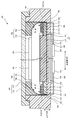
- FIG. 3 is a cross-sectional view of the contact image sensor according to the first embodiment when viewed from the sub-scanning direction. It is a figure which expands and shows the edge part vicinity of the light guide in FIG. 2 is a diagram illustrating a functional configuration of a control unit according to Embodiment 1.
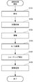
- FIG. 3 is a flowchart showing a flow of reading processing according to the first embodiment.
- FIG. 4 is a flowchart showing a flow of output correction processing according to the first embodiment. It is sectional drawing which looked at the contact
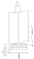
- FIG. 10 is a perspective view showing the vicinity of an end portion of a light guide according to a sixth embodiment.
- the contact image sensor according to the first embodiment of the present invention is a device that reads an image of an original M as a reading target.
- a reading target For example, a facsimile, a copier, a scanner, a multifunction peripheral, a financial terminal, an industrial inspection device, or the like.
- the reading target is not limited to the original M, and may be, for example, a mark sheet, a banknote, a check, or other securities.
- the contact image sensor irradiates light to a linear reading unit extending in the main scanning direction which is predetermined as a place where the document M is brought into close contact. As a result, linear light is irradiated onto the original M that is in close contact with the reading unit.
- the contact image sensor receives reflected light from the document M, and reads an image of a linear portion of the document M irradiated with light.
- the contact image sensor reads the image on the reading surface of the document M by sequentially reading the image of the linear portion of the document M while the contact image sensor and the document M move relatively in the sub-scanning direction.
- the sub-scanning direction is a direction that intersects the main scanning direction, and is a direction perpendicular to the main scanning direction in the present embodiment.
- the contact image sensor 100 includes a frame 101, a transmissive body 102, a lens body 103, two light guides 104, four light source units 105, and four corrections.
- a light receiving unit 106, a holding body 107, a sensor body 108, and a control unit 109 are provided.
- the frame 101 is composed of a rectangular bottom having a main scanning direction as a longitudinal direction and a sub-scanning direction as a short direction, and a side wall extending upward from the outer edge thereof, and an open top.
- a black resin for example, a black resin.
- the bottom of the frame 101 has an opening extending in the longitudinal direction at the center in the short direction.
- a transmission body 102 is attached to the upper part of the frame 101 so as to close the upper part thereof.
- a sensor body 108 is attached to the outside of the bottom of the frame 101.
- the lens body 103, the light guide body 104, the light source unit 105, the correction light receiving unit 106, and the holding body 107 are accommodated in a space that is generally sealed by the frame 101, the transmission body 102, and the lens body 103.
- the location where the control unit 109 is attached may be determined as appropriate, in this embodiment, the control unit 109 is attached to the lower surface of the sensor body 108.
- the transmissive member 102 is a member that transmits light irradiated to the document M arranged in close contact with the reading unit 110 and light reflected by the document M, and includes a transmissive unit 111 and a holding frame 112.
- the transmission unit 111 has a linear reading unit 110 extending in the main scanning direction on the outer surface, and is made of, for example, a resin such as acrylic or polycarbonate, glass, or the like. It is a translucent, desirably a transparent flat plate.
- the holding frame 112 is, for example, a resin frame that surrounds and holds the periphery of the transmission part 111. As shown in FIG. 3, which is a cross-sectional view of the contact image sensor 100 viewed from the main scanning direction, and FIG. 4, which is a cross-sectional view of the contact image sensor 100 viewed from the sub-scanning direction. Is attached in close contact with the upper portion of the frame 101. Thereby, the holding frame 112 closes the upper part of the frame 101 so that dust or the like does not enter.
- the lens body 103 is a member that converges the light reflected from the document M onto the sensor body 108, and extends in the main scanning direction as shown in FIG.
- the lens body 103 has a plurality of rod lenses arranged in the longitudinal direction. Each rod lens is disposed above the opening at the bottom of the frame 101 as shown in FIG.
- Each of the light guides 104 is an elongated cylindrical member that propagates light incident on the light guide body 104 in the longitudinal direction.
- Each of the light guides 104 includes an incident part 113, a first emission part 114, and a second emission part 115, as shown in FIG. 5 in which the vicinity of the end of the light guide 104 in FIGS. 3 and 4 is enlarged.
- a light diffusion layer 116 is provided.
- the incident portion 113 is a portion that allows light emitted from the light source portion 105 to enter the inside of the outer surface of the light guide 104.
- the first emitting unit 114 is a part of the outer surface of the light guide 104 that emits light to the document M.
- the second emission unit 115 is a part of the outer surface of each light guide 104 from which light to the correction light receiving unit 106 is emitted.
- the light diffusing layer 116 is a portion that reflects and diffuses the light propagating through the light guide 104.
- the light diffusing layer 116 is coated with a light reflective material such as a white pigment, and the surface of the light guide 104 is roughened and serrated. The prism shape processing or pyramid emboss shape processing is used.
- the incident portion 113 and the second emitting portion 115 are formed at each end portion of each light guide body 104.
- the first emission part 114 and the light diffusion layer 116 are part of the outer peripheral surface extending in the main scanning direction, and are formed substantially symmetrically via the long axis of the light guide 104.
- Each of the light source units 105 is a member that emits light for irradiating the document M, and includes four LED (Light Emitting Diode) chips 117, an LED substrate 118, a heat conductive sheet 119, and a heat dissipation plate 120. Have.
- LED Light Emitting Diode
- Each LED chip 117 is a light source that emits visible light (red, blue, green, yellow), ultraviolet light having a wavelength of about 365 nm, infrared light having a wavelength of about 700 to 1000 nm, and the like.
- Four LED chips 117 form one set, and light emitted from one set of LED chips 117 enters from the incident portion 113 of one light guide 104.
- the two light source sections 105 have one LED board 118 in common. Therefore, eight LED chips 117 as light sources that emit light are mounted on the surface of the LED substrate 118.
- the LED chip 117 may be directly mounted on the LED substrate 118 or may be provided as a package mounted on the LED substrate 118.
- the heat conductive sheet 119 and the heat sink 120 are provided on the back surface of the LED substrate 118.
- the heat conductive sheet 119 and the heat dissipation plate 120 can dissipate heat generated in the LED chip 117 to the outside, and the LED chip 117 can emit light efficiently.
- Each of the correction light receiving units 106 is configured by a photodiode having light receiving sensitivity to light emitted from the LED chip 117, and outputs an electrical signal corresponding to the amount of received light.
- One correction light receiving unit 106 is provided in association with one set of LED chips 117. Therefore, in the present embodiment, two correction light receiving portions 106 are mounted on the surface of one LED substrate 118.
- the correction light receiving unit 106 may be directly mounted on the LED board 118 or may be provided as a package mounted on the LED board 118 together with the LED chip 117.
- the holding body 107 is a member for fixing the two light guide bodies 104 and the light source section 105 provided with the correction light receiving section 106 in the frame 101, and includes two support sections 121 and two holder sections 122.
- Each of the two support parts 121 is provided so as to support the longitudinal direction of one light guide 104 in the main scanning direction and to cover the outer peripheral surface of the light guide 104 excluding the first emission part 114.
- Each of the holder parts 122 has two holes into which the end parts of the light guide 104 are fitted. Protrusions are provided on the outer peripheral surface in the vicinity of each end of each light guide 104. When each end fits into a hole in the holder part 122, each protrusion engages with the hole. As a result, the movement of each light guide 104 in the main scanning direction and the rotation around the major axis in the frame 101 are restricted.
- Each of the support parts 121 supports one light guide 104, one end of the two light guides 104 fits in each of the holes of one holder part 122, and each of the holes of the other holder part 122
- the two light guides 104 and the holding body 107 are fixed in the frame 101 with the other ends of the two light guides 104 fitted.
- the two light guides 104 are fixed parallel to each other with the holding body 107 facing the longitudinal direction in the main scanning direction, and are arranged symmetrically via the lens body 103.
- the light guide so that the light propagating through the interior, reflected by the light diffusion layer 116 and diffused is emitted from the first emitting unit 114 to the reading unit 110, that is, toward the document M.
- Each of 104 is arranged.
- the light diffusion layer 116 may be formed on each support portion 121 instead of each light guide 104 or together with each light guide 104.
- the LED substrate 118 is attached to each of the holder portions 122 with the surface thereof facing the end portion of the light guide body 104.
- a set of four LED chips 117 and one correction light-receiving unit 106 are arranged to face each other at the ends of the two light guides 104.
- one of the LED chips 117 is disposed at the center of the light guide 104, and the other three LEDs are arranged at the same distance from the center above and to the left and right.
- a chip 117 is arranged.
- the correction light receiving unit 106 is located away from the transmission unit 111, that is, below the center of the light guide 104, in order to make it difficult to receive light entering from the outside of the contact image sensor 100 through the transmission unit 111 described in detail later. Placed in.
- a sensor body (reading light receiving unit) 108 receives reflected light from the document M through the lens body 103 and performs photoelectric conversion to generate and output image data indicating the read image. Since the image data handled by the sensor body 108 is analog data, it is hereinafter referred to as analog image data. As shown in FIGS. 3 and 4, the sensor body 108 includes a sensor substrate 123, a plurality of reading conversion units 124, and an amplification unit 125.
- the sensor substrate 123 is a rectangular substrate having the same size as the bottom of the frame 101, and the upper surface thereof is disposed to face the outer surface of the bottom of the frame 101, and is fixed to the frame 101 by, for example, screwing or the like. .
- the reading conversion unit 124 includes a plurality of photodiodes, capacitors, and the like, has light receiving sensitivity with respect to light emitted from the LED chip 117, generates an electrical signal corresponding to each received light, and is obtained by photoelectric conversion. Output as analog image data. More specifically, the reading conversion unit 124 generates an electromotive force according to the received light, and generates an electric signal corresponding to the received light by photoelectric conversion that converts light energy into an electric signal.
- a plurality of reading conversion units 124 are arranged on the upper surface of the sensor substrate 123 in the main scanning direction. When the sensor substrate 123 is fixed to the frame 101, the reading conversion unit 124 is positioned in the opening at the bottom of the frame 101 or below the opening.
- the amplifying unit 125 is composed of, for example, a circuit provided on the sensor substrate 123, amplifies the electric signal generated by the reading conversion unit 124, and outputs the amplified electric signal.
- the amplification unit 125 outputs the generated electrical signal as amplified analog image data.
- the control unit 109 transmits / receives various signals (data) to / from the reading conversion unit 124, the light source unit 105, the correction light receiving unit 106, and the like, thereby correcting bright output, and image data indicating an image of the document M. Execute processing to output.
- the image data output from the control unit 109 is digital data.
- image data that is digital data is referred to as digital image data.
- the bright output is the content (each pixel value or the like) indicated by the image data generated by the contact image sensor 100 when a white reading target is read.
- the reading target is white.
- the image data generated by the reading unit 110 indicates the content.
- the control unit 109 is configured from an electric circuit, a microcomputer, a flash memory, or the like, or a combination thereof. As shown in FIG. 6, the control unit 109 functionally includes an LED driving unit 126, a correction A / D (Analog / Digital) conversion unit 127, a storage unit 128, and a comparison correction unit (correction unit) 129. A synchronization control unit 130, a reading A / D conversion unit 131, a shading correction unit 132, and an image processing unit 133.
- a synchronization control unit 130 a reading A / D conversion unit 131, a shading correction unit 132, and an image processing unit 133.
- the LED drive unit 126 causes the LED chip 117 to emit light while controlling the amount of light by controlling, for example, the magnitude of the current flowing through the LED chip 117 and the time during which the current flows through the LED chip 117.
- the correction A / D conversion unit 127 converts the electrical signal that is analog data output from the correction light receiving unit 106 into reference data that is digital data.
- the storage unit 128 stores reference data indicating a bright output reference.
- the reference data is stored in the storage unit 128 when the contact image sensor 100 is shipped, for example, when the contact image sensor 100 is operated for the first time.
- the reference data for example, the amount of light received from the LED chip 117 by the correction light receiving unit 106 at the time of storage is set.
- the comparison correction unit 129 compares the reference data generated by the correction A / D conversion unit 127 with the standard data in the storage unit 128. Then, the comparison / correction unit 129 causes the LED driving unit 126 to change the time during which the current flows to the LED chip 117 and the magnitude of the current so that the content of the reference data satisfies the standard indicated by the standard data. Thereby, since the light quantity of the light which LED chip 117 emits is changed, a bright output can be corrected. Specifically, for example, the bright output is corrected so that each value indicated by the reference data is equal to the value indicated by the reference data.
- the comparison correction unit 129 may correct the bright output based on the reference data of the analog data and the standard data corresponding to the reference data.
- the synchronization control unit 130 outputs a synchronization signal for synchronizing the light emission of the LED chip 117 and one or both of the photoelectric conversion of the reading conversion unit 124 and the A / D conversion of the correction A / D conversion unit 127 to the LED.
- the data is output to the drive unit 126 and one or both of the reading conversion unit 124 and the correction A / D conversion unit 127.
- the reading A / D converter 131 converts the analog image data amplified by the amplifier 125 of the sensor body 108 into digital data, thereby generating digital image data.
- the shading correction unit 132 obtains digital image data from the reading A / D conversion unit 131 and performs shading correction to generate digital image data that has been subjected to shading correction.
- the image processing unit 133 acquires the digital image data subjected to the shading correction by the shading correction unit 132, performs predetermined image processing, and generates and outputs the image data.
- the image processing unit 133 compares the generated image data with the determination data stored in advance so that the reading target is the inspection standard. It may be determined whether or not it is suitable.
- the determination data indicates a criterion for determining whether or not the reading target meets the inspection standard. Then, the image processing unit 133 may output data indicating the determination result.
- the image processing unit 133 may identify a mark selected on the mark sheet and output data indicating the identified result. Specifically, for example, the image processing unit 133 identifies the mark selected on the mark sheet by specifying the position of the mark selected on the mark sheet from the generated image data and collating it with the previously stored identification data. To do.
- the identification data indicates, for example, a position where each mark (number, alphabet, symbol, etc.) is indicated on the mark sheet.
- the contact image sensor 100 performs a general reading process as shown in FIG. 7 in response to a reading synchronization signal from the synchronization control unit 130 in a state where the document M is in close contact with the reading unit 110.
- the contact image sensor 100 reads an image on the reading surface of the document M by repeatedly executing the reading process while moving relative to the document M in the sub-scanning direction while the document M is in close contact with the reading unit 110. Then, image data indicating the image is generated and output.
- the LED driving unit 126 when the LED driving unit 126 receives the reading synchronization signal from the synchronization control unit 130, the LED driving unit 126 causes the LED chip 117 to emit light (step S101). At this time, the LED driving unit 126 controls the amount of light emitted from the LED chip 117 by controlling the current flowing through the LED chip 117 and the time during which the current flows through the LED chip 117 to a predetermined size and time length. To control.
- the light emitted from the LED chip 117 enters the light guide 104 from the end of the light guide 104 facing the LED chip 117.
- the light that has entered the light guide 104 propagates in the main scanning direction in the light guide 104 while being totally reflected.
- a part of the light scattered and reflected by the light diffusion layer 116 is emitted from the first emission part 114.
- the support portion 121 of the holding body 107 is provided so as to cover the outer peripheral surface of the light guide body 104 excluding the first emission portion 114 as described above. Therefore, the light leaking from the outer peripheral surface other than the first emitting portion 114 to the outside of the light guide 104 without being totally reflected inside the light guide 104 is reflected by the support portion 121. Therefore, the extraction efficiency of light emitted to the document M to be read can be improved by the support portion 121 that covers the outer peripheral surface of the light guide body 104 excluding the first emission portion 114.
- the light emitted from the first emission unit 114 irradiates the document M that is in close contact with the reading unit 110 via the transmission unit 111 and is reflected by the document M.
- the light reflected by the document M passes through the lens body 103 via the transmission unit 111.
- the light that has passed through the lens body 103 is converged and received by each light receiving unit of the reading conversion unit 124.
- Each of the reading conversion units 124 performs photoelectric conversion to generate an electrical signal corresponding to the received light (step S102).
- Each of the reading conversion units 124 outputs analog image data obtained by photoelectric conversion.
- the analog image data output from the plurality of reading conversion units 124 included in the sensor body 108 indicates an image of a linear portion of the document M that is in close contact with the reading unit 110.
- the amplification unit 125 amplifies the electrical signal output from each of the reading conversion units 124, that is, the analog image data obtained by photoelectric conversion (step S103).
- the amplifying unit 125 outputs the amplified analog image data.
- the reading A / D conversion unit 131 converts the amplified analog image data into digital image data (step S104).
- the reading A / D converter 131 outputs digital image data obtained by the conversion.
- the shading correction unit 132 performs predetermined shading correction processing on the digital image data output from the reading A / D conversion unit 131 (step S105).
- the shading correction unit 132 outputs digital image data subjected to shading correction.
- the image processing unit 133 performs predetermined image processing on the digital image data subjected to the shading correction by the shading correction unit 132 (step S106).
- the image processing unit 133 outputs digital image data subjected to image processing.
- the image processing unit 133 ends the reading process.
- read data, digital conversion data, shading correction data, and image data indicating an image appearing on the linear portion of the document M that is in close contact with the reading unit 110 are sequentially generated.
- the contact image sensor 100 repeatedly performs the reading process while moving relatively to the document M in the sub-scanning direction in a state where the document M is in close contact with the reading unit 110, thereby displaying an image on the reading surface of the document M. Image data can be obtained.
- the contact image sensor 100 executes an output correction process shown in FIG.
- the output correction process is a process for correcting the bright output, and is executed in response to the output correction synchronization signal from the synchronization control unit 130.
- This synchronization signal for output correction may be, for example, common to the above-described synchronization signal for reading, may be output when the contact image sensor 100 is activated, and is output in response to an operation on an operation unit (not shown). May be.
- the LED driving unit 126 when receiving the output correction synchronization signal from the synchronization control unit 130, the LED driving unit 126 causes the LED chip 117 to emit light (step S111). At this time, the LED drive unit 126 controls the amount of light emitted from the LED chip 117 in the same manner as the light emission process in step S101.
- step S111 and step S101 are the same processing.
- the light emitted from the LED chip 117 opposed to one end of the light guide 104 propagates through the light guide 104 and is received by the correction light receiving unit 106 opposed to the other end of the light guide 104.
- the correction light receiving unit 106 performs photoelectric conversion to generate an electrical signal corresponding to the received light (step S112).
- the correction light receiving unit 106 outputs an electrical signal that is analog data generated by photoelectric conversion.
- the correction A / D conversion unit 127 When receiving the synchronization signal from the synchronization control unit 130, the correction A / D conversion unit 127 generates reference data by performing A / D conversion into an electrical signal that is analog data acquired from the correction light receiving unit 106 at that time. (Step S113).
- This reference data is digital data indicating the amount of light received from the LED chip 117 by the correction light receiving unit 106 when receiving the synchronization signal from the synchronization control unit 130.
- the comparison correction unit 129 acquires the reference data from the correction A / D conversion unit 127 and reads the reference data from the storage unit 128 (step S114).
- the comparison and correction unit 129 compares the reference data with the standard data (step S115).
- the comparison correction unit 129 determines whether or not the bright output needs to be corrected based on the comparison result (step S116). For example, when the values indicated by the reference data and the reference data are the same, the comparison correction unit 129 determines that the bright output correction is not necessary (step S116; No), and ends the output correction process.
- the comparison correction unit 129 determines that the bright output needs to be corrected (step S116; Yes).
- the comparison correction unit 129 controls the LED driving unit 126 so that the values indicated by the reference data and the standard data are the same. Specifically, the comparison correction unit 129 adjusts the amount of light from the LED chip 117 by causing the LED driving unit 126 to change the magnitude of the current flowing through the LED chip 117 and the time during which the current flows through the LED chip 117. . Thereby, the comparison correction unit 129 corrects the bright output (step S117) and ends the output correction process.
- the correction light receiving unit 106 directly receives the light propagated through the light guide 104.
- the bright output is corrected based on the reference data corresponding to the direct light received by the correction light receiving unit 106. Therefore, the output correction process can be executed at any time, for example, depending on the light emitted in the reading process, regardless of the presence or absence of the document M. Therefore, not only the long-term deterioration of the LED chip 117 but also the light output can be corrected even when the amount of light from the LED chip 117 changes due to environmental temperature, short-term factors, etc. it can. Therefore, a stable bright output can be obtained.
- the correction light receiving unit 106 receives direct light that has propagated through the light guide 104 rather than indirect light that is emitted from the light guide 104 and reflected by a member such as a platen roller or a white reference tape. Therefore, it is possible to obtain reference data that accurately reflects the amount of light emitted from the LED chip 117 without being affected by deterioration or contamination of intervening members. Therefore, a stable bright output can be obtained.
- the image data output from the sensor body 108 may fluctuate transiently.
- the bright output is corrected based on the reference data corresponding to the direct light received by the correction light receiving unit 106, and therefore, the image data output from the sensor body 108 may be subjected to a transient change. rare. Accordingly, it is possible to correct the bright output even during warm-up after power-on and obtain a stable bright output.
- the image quality of the read image By obtaining stable bright output, the image quality of the read image, the accuracy of discrimination in inspection, the accuracy of identifying the mark selected on the mark sheet, etc. are improved according to the application of the device in which the contact image sensor 100 is mounted. It becomes possible to make it.
- the correction light-receiving unit 106 is not directly irradiated with the external light transmitted through the transmissive body 102 or the reflected light from the original M, and the external light or the reflected light is received by the correction light-receiving unit 106. At least through the light guide 104. Therefore, it is possible to reduce the influence of external light or reflected light on the light received by the correction light receiving unit 106. As a result, the accuracy of the reference data can be improved, and a stable bright output can be obtained.
- the correction light receiving unit 106 directly receives the light propagated through the light guide 104. Therefore, by adopting the correction light-receiving unit 106 having sensitivity to ultraviolet light, it is possible to obtain an accurate ultraviolet light reference output even when the LED chip 117 emits ultraviolet light. Therefore, a stable bright output can be obtained even with ultraviolet light. Similarly, a stable bright output can be obtained even with infrared light.
- the bright output is corrected by causing the LED driving unit 126 to control the amount of light emitted from the LED chip 117.
- the LED driving unit 126 is provided in a general contact image sensor 100. Therefore, in order to correct the bright output, it is possible to suppress an increase in the number of parts, and it is possible to obtain a stable bright output with a simple configuration.
- Embodiment 2 FIG. In the contact image sensor according to the present embodiment, the arrangement of the light source unit and the correction light receiving unit is different from that of the contact image sensor 100 according to the first embodiment.
- the contact image sensor 200 has one end of the light guide 104 as shown in FIG. 9 which is a cross-sectional view seen from the main scanning direction and FIG. 10 which is a cross-sectional view seen from the sub-scanning direction.
- the light source unit 205 includes four LED chips 217 provided on the LED substrate, and each LED chip 217 is formed from the center of one end of the light guide 104.
- the light guide 104 is disposed at an equidistant position in the vertical and horizontal directions so as to face one end of the light guide 104.
- the contact image sensor 200 operates in the same manner as in the first embodiment.
- the light emitted from the light source unit 205 enters from one end (incident unit 213) of the light guide 104 and propagates through the light guide 104.
- a part of the light propagating through the light guide 104 is emitted from the other end (second emission part 215) of the light guide 104 and directly received by the correction light receiving part 206.
- the correction light receiving unit 206 generates an electrical signal corresponding to the received light, and corrects the bright output based on reference data generated from the electrical signal. Therefore, as in the first embodiment, it is possible to obtain a stable bright output.
- the LED substrate 218 having the LED chip 217 is disposed at one end of each light guide 104, and the correction light receiving unit 206 is disposed, for example, together with the substrate at the other end. Since the heat generation from the correction light receiving unit 206 is relatively small, it is not necessary to provide the heat conductive sheet 119 or the heat radiating plate 120 on the substrate of the correction light receiving unit 206. Therefore, the number of components constituting the contact image sensor 200 can be reduced, and the contact image sensor 200 can be made compact.
- Embodiment 3 In the contact image sensor according to the present embodiment, the arrangement of the correction light receiving units is different from that of the contact image sensor 200 according to the second embodiment.
- the LED chip 217 of the light source unit 205 similar to that of the second embodiment is disposed at one end of each light guide 104.
- a hole 334 extending downward from the second emitting portion 315 formed on the outer peripheral surface near the other end of each light guide 104 to the upper surface of the sensor substrate 123 is formed in the support portion 121 and the frame 101. Is provided.
- the contact image sensor 300 operates in the same manner as in the first embodiment.
- light emitted from the light source unit 205 enters from one end (incident part) of the light guide 104 and propagates through the light guide 104 as in the second embodiment.
- a part of the light propagating through the light guide 104 is emitted downward from a part of the outer peripheral surface in the vicinity of the other end of the light guide 104 (second emission part 315), and directly by the correction light receiving part 306. Is received.
- the correction light receiving unit 306 generates an electrical signal corresponding to the received light, and corrects the bright output based on reference data generated from the electrical signal. Therefore, as in the first embodiment, it is possible to obtain a stable bright output.
- the correction light receiving unit 306 is disposed in the vicinity of each end portion of each light guide 104, but the distance from the transmissive member 102 is that of the correction light receiving unit 306 in the first embodiment. It is farther than the correction light receiving unit 106 according to the above. Therefore, it is possible to further reduce the influence of the external light or the reflected light from the document M on the light received by the correction light receiving unit 306. As a result, the accuracy of the reference data can be improved, and a stable bright output can be obtained.
- Embodiment 4 FIG.
- the shape of the light guide and the arrangement of the correction light receiving unit are different from those of the contact image sensor 100 according to the first embodiment.
- the light guide 404 is a member extending in the main scanning direction, and extends from the center toward both ends. It becomes thinner gradually.
- a V-shaped notch 435 is provided at the upper center.
- the cross section of the light guide body 404 viewed from the main scanning direction is, for example, an isosceles trapezoidal shape having a wide lower part.
- a second emitting portion 415 is provided on the lower surface of the body 404.
- the light diffusing layer 416 is provided on the lower surface of the light guide body 404 excluding the second emitting portion 415.
- the light source unit 405 is disposed in the vicinity of each end of the light guide 404, and the LED chip of the light source 405 faces each end of the light guide 404.
- the correction light receiving unit 406 is the center of the light guide 404 in the main scanning direction, and is disposed so as to face or be in contact with the lower surface.
- the contact image sensor 400 operates in the same manner as in the first embodiment. Accordingly, light emitted from the light source unit 405 is incident from each end portion (incident unit 413) of the light guide 404 and propagates through the light guide 404 toward the center. A part of the light propagated to the vicinity of the center of the light guide 404 is reflected downward by the V-shaped cutout, and is emitted from the lower surface (second emission part 415) near the center of the light guide 404, Light is received by the correction light receiving unit 406. Then, the correction light receiving unit 406 generates an electrical signal corresponding to the received light, and corrects the bright output based on reference data generated from the electrical signal. Therefore, as in the first embodiment, it is possible to obtain a stable bright output.
- Embodiment 5 FIG.
- the shape of the light guide and the arrangement of the light source unit and the correction light receiving unit are different from those of the contact image sensor 100 according to Embodiment 1.
- FIG. 13 shows a view of the contact image sensor 500 according to the present embodiment as viewed from the main scanning direction.
- Each of the light guides 504 is a member having the same cross-sectional shape and extending in the main scanning direction, and integrally includes a front stage portion 536 located on the center side of the frame 101 and a rear stage portion 537 located on the side wall side of the frame 101. Have.
- the front stage 536 has an end perpendicular to the main scanning direction, and a first emission part 514 is provided on the upper part.
- the rear stage portion 537 has an end portion that forms an acute angle with the surface where the rear stage portion 537 and the front stage portion 536 are joined, as shown in FIG.
- a light diffusion layer 516 is provided below the front stage part 536 and the rear stage part 537, and a first emission part 514 is provided above the front stage part 536.
- the LED chip 517 of the light source unit 505 and the correction light receiving unit 506 are opposed to each end of the front stage 536 and the rear stage 537.
- the correction light receiving unit 506 is provided on the LED substrate 518 included in the light source unit 505 as in the first embodiment.
- the contact image sensor 500 operates in the same manner as in the first embodiment. Accordingly, light emitted from the light source unit 505 is incident from one end (incident unit 513) of the front stage 536 of the light guide 504 and propagates through the light guide 504. Part of the light propagating through the light guide 504 is emitted downward from the other end (second emission part 515) of the rear stage part 537 of the light guide 504, and is directly received by the correction light receiving part 506. The Then, the correction light receiving unit 506 generates an electrical signal corresponding to the received light, and corrects the bright output based on reference data generated from the electrical signal. Therefore, as in the first embodiment, it is possible to obtain a stable bright output.
- Embodiment 6 FIG.
- the shape of the light guide and the arrangement of the light source unit and the correction light receiving unit are different from those of the contact image sensor 100 according to Embodiment 1.
- the light guide 604 has an isosceles trapezoidal cross section in which the width in the sub scanning direction becomes narrower from the upper side to the lower side, and extends in the main scanning direction. It is a member.
- a light diffusion layer 616 is provided below the light guide 604, and a first light emitting portion 614 is provided above the light guide 604.
- the end portion of the light guide 604 has a pair of inclined surfaces, and these inclined surfaces are provided symmetrically via a plane that faces up and down parallel to the main scanning direction.
- the light source unit 605 includes an LED substrate 618 and an LED chip 617 provided on the LED substrate 618 as shown in FIG. 17 which is an enlarged view of the vicinity of the end of the light guide 604 as viewed from above.
- the LED chip 617 is disposed to face one of the inclined surfaces of the light guide 604.
- the correction light receiving unit 606 is provided on the LED substrate 618 and is disposed to face the other inclined surface of the light guide 604.
- the end portion of the light guide 604 has a plurality of pairs of inclined surfaces that are symmetric via a plurality of different surfaces.
- a correction light receiving unit 606 is provided on one of the inclined surfaces, and each of the other inclined surfaces.
- the LED chip 617 may be opposed.
- the contact image sensor 600 operates in the same manner as in the first embodiment. Accordingly, light emitted from the light source unit 605 is incident from one of the inclined surfaces (incident unit 613) provided at one end of the light guide 604 and propagates through the light guide 604. Part of the light propagating through the light guide 604 is emitted from the other inclined surface (second emission part 615) provided at the other end of the light guide 604, and directly by the correction light receiving part 606. Received light. Then, the correction light receiving unit 606 generates an electrical signal corresponding to the received light, and corrects the bright output based on reference data generated from the electrical signal. Therefore, as in the first embodiment, it is possible to obtain a stable bright output.
- Embodiment 7 FIG.
- the shape of the light guide and the arrangement of the light source unit and the correction light receiving unit are different from those of the contact image sensor 100 according to Embodiment 1.
- FIG. 18 is an enlarged view of the light guide end portion 739 when the contact image sensor 700 is viewed from the sub-scanning direction.
- the light guide end portion 739 is a portion located in the vicinity of the end portion of the light guide 704 and has an extending portion 740 extending in the main scanning direction.
- the extending part 740 has an extending end part facing downward and an inclined surface having a shape obtained by extruding a part of an elliptical contour in the sub-scanning direction.
- the light source unit 705 and the correction light receiving unit 706 are opposed to the extending end.
- the LED chip 717 of the light source unit 705 is provided on the LED substrate 718, and the correction light receiving unit 706 is also provided on the LED substrate 718.
- the contact image sensor 700 operates in the same manner as in the first embodiment. Accordingly, light emitted from the light source unit 705 is incident from one of the extending end portions (incident unit 713) of the light guide 704 and propagates through the light guide 704. Part of the light propagating through the light guide 704 is emitted from the other of the extending end portions of the light guide 704 (second emission part 715) and is directly received by the correction light receiving part 706.
- the correction light receiving unit 706 generates an electrical signal corresponding to the received light, and corrects the bright output based on reference data generated from the electrical signal. Therefore, as in the first embodiment, it is possible to obtain a stable bright output.
- Embodiment 8 FIG.
- the bright output is corrected by adjusting the amount of light from the LED chip 117.
- the amplification unit corrects the bright output by adjusting the output level from the sensor body.
- the contact image sensor according to the present embodiment has substantially the same configuration as that of the contact image sensor 100 according to the first embodiment.
- the configuration of the control unit 809 of the contact image sensor according to the present embodiment is different from the control unit 109 according to the first embodiment.
- the control unit 809 according to the present embodiment includes a comparison correction unit 829 instead of the comparison correction unit 129 according to the first embodiment.
- the comparison correction unit 829 causes the amplification unit 125 to change the output level so that the content of the reference data satisfies the standard indicated by the standard data. As a result, the content of the analog image data output from the sensor body 108 is changed, so that the bright output can be corrected.
- the contact image sensor according to the present embodiment executes the same reading process and output correction process as in the first embodiment.
- the comparison correction unit 829 adjusts the content of the analog image data by causing the amplification unit 125 to change the output level.
- the bright output is corrected by causing the amplification unit 125 to control the output level.
- the amplifying unit 125 is provided in a general contact image sensor. For this reason, it is possible to suppress an increase in the number of parts for correcting the bright output, and it is possible to obtain a stable bright output with a simple configuration.
Landscapes
- Engineering & Computer Science (AREA)
- Multimedia (AREA)
- Signal Processing (AREA)
- Physics & Mathematics (AREA)
- Optics & Photonics (AREA)
- Facsimile Scanning Arrangements (AREA)
- Facsimile Heads (AREA)
- Image Input (AREA)
Priority Applications (3)
| Application Number | Priority Date | Filing Date | Title |
|---|---|---|---|
| CN201380042516.6A CN104541495B (zh) | 2012-08-10 | 2013-07-10 | 接触式图像传感器、接触式图像传感器用输出校正装置以及接触式图像传感器用输出校正方法 |
| US14/418,185 US9516193B2 (en) | 2012-08-10 | 2013-07-10 | Contact image sensor, output correction device for contact image sensor, and output correction method for contact image sensor |
| EP13828729.7A EP2884729B1 (en) | 2012-08-10 | 2013-07-10 | Contact image sensor |
Applications Claiming Priority (2)
| Application Number | Priority Date | Filing Date | Title |
|---|---|---|---|
| JP2012-178137 | 2012-08-10 | ||
| JP2012178137A JP6291707B2 (ja) | 2012-08-10 | 2012-08-10 | 密着イメージセンサ、密着イメージセンサ用出力補正装置及び密着イメージセンサ用出力補正方法 |
Publications (1)
| Publication Number | Publication Date |
|---|---|
| WO2014024623A1 true WO2014024623A1 (ja) | 2014-02-13 |
Family
ID=50067863
Family Applications (1)
| Application Number | Title | Priority Date | Filing Date |
|---|---|---|---|
| PCT/JP2013/068833 Ceased WO2014024623A1 (ja) | 2012-08-10 | 2013-07-10 | 密着イメージセンサ、密着イメージセンサ用出力補正装置及び密着イメージセンサ用出力補正方法 |
Country Status (5)
| Country | Link |
|---|---|
| US (1) | US9516193B2 (https=) |
| EP (1) | EP2884729B1 (https=) |
| JP (1) | JP6291707B2 (https=) |
| CN (1) | CN104541495B (https=) |
| WO (1) | WO2014024623A1 (https=) |
Families Citing this family (43)
| Publication number | Priority date | Publication date | Assignee | Title |
|---|---|---|---|---|
| US9335604B2 (en) | 2013-12-11 | 2016-05-10 | Milan Momcilo Popovich | Holographic waveguide display |
| US11726332B2 (en) | 2009-04-27 | 2023-08-15 | Digilens Inc. | Diffractive projection apparatus |
| WO2016020630A2 (en) | 2014-08-08 | 2016-02-11 | Milan Momcilo Popovich | Waveguide laser illuminator incorporating a despeckler |
| EP2748670B1 (en) | 2011-08-24 | 2015-11-18 | Rockwell Collins, Inc. | Wearable data display |
| US20150010265A1 (en) | 2012-01-06 | 2015-01-08 | Milan, Momcilo POPOVICH | Contact image sensor using switchable bragg gratings |
| EP2842003B1 (en) | 2012-04-25 | 2019-02-27 | Rockwell Collins, Inc. | Holographic wide angle display |
| US9933684B2 (en) | 2012-11-16 | 2018-04-03 | Rockwell Collins, Inc. | Transparent waveguide display providing upper and lower fields of view having a specific light output aperture configuration |
| US9727772B2 (en) | 2013-07-31 | 2017-08-08 | Digilens, Inc. | Method and apparatus for contact image sensing |
| JP2015136043A (ja) * | 2014-01-17 | 2015-07-27 | 株式会社東芝 | 画像読取装置 |
| JP6359898B2 (ja) * | 2014-07-03 | 2018-07-18 | シャープ株式会社 | 照明装置、画像読取装置及びそれを備えた画像形成装置 |
| WO2016042283A1 (en) | 2014-09-19 | 2016-03-24 | Milan Momcilo Popovich | Method and apparatus for generating input images for holographic waveguide displays |
| JP2016100633A (ja) * | 2014-11-18 | 2016-05-30 | キヤノン・コンポーネンツ株式会社 | 照明装置、イメージセンサユニット、画像読取装置および紙葉類識別装置 |
| US10437064B2 (en) | 2015-01-12 | 2019-10-08 | Digilens Inc. | Environmentally isolated waveguide display |
| CN105872279B (zh) * | 2015-02-10 | 2018-11-09 | 佳能元件股份有限公司 | 图像传感器单元、纸张识别装置、图像读取以及形成装置 |
| US9632226B2 (en) | 2015-02-12 | 2017-04-25 | Digilens Inc. | Waveguide grating device |
| JP6100815B2 (ja) | 2015-02-18 | 2017-03-22 | 株式会社Pfu | 光源ユニット |
| US10591756B2 (en) * | 2015-03-31 | 2020-03-17 | Digilens Inc. | Method and apparatus for contact image sensing |
| JP1553848S (https=) * | 2015-06-18 | 2016-07-11 | ||
| JP1553413S (https=) * | 2015-06-18 | 2016-07-11 | ||
| JP1553412S (https=) * | 2015-06-18 | 2016-07-11 | ||
| JP1553847S (https=) * | 2015-06-18 | 2016-07-11 | ||
| JP1553414S (https=) * | 2015-06-18 | 2016-07-11 | ||
| JP1553417S (https=) * | 2015-06-18 | 2016-07-11 | ||
| JP1553846S (https=) * | 2015-06-18 | 2016-07-11 | ||
| JP1553845S (https=) * | 2015-06-18 | 2016-07-11 | ||
| WO2017060665A1 (en) | 2015-10-05 | 2017-04-13 | Milan Momcilo Popovich | Waveguide display |
| JP6895451B2 (ja) | 2016-03-24 | 2021-06-30 | ディジレンズ インコーポレイテッド | 偏光選択ホログラフィー導波管デバイスを提供するための方法および装置 |
| EP3548939A4 (en) | 2016-12-02 | 2020-11-25 | DigiLens Inc. | UNIFORM OUTPUT LIGHTING WAVEGUIDE DEVICE |
| US10545346B2 (en) | 2017-01-05 | 2020-01-28 | Digilens Inc. | Wearable heads up displays |
| CN107426511A (zh) * | 2017-05-17 | 2017-12-01 | 威海华菱光电股份有限公司 | 图像传感器及具有其的图像传感扫描系统 |
| JP7404243B2 (ja) | 2018-01-08 | 2023-12-25 | ディジレンズ インコーポレイテッド | 導波管セル内のホログラフィック格子の高スループット記録のためのシステムおよび方法 |
| JP7456929B2 (ja) | 2018-01-08 | 2024-03-27 | ディジレンズ インコーポレイテッド | 導波管セルを製造するためのシステムおよび方法 |
| CN114721242B (zh) | 2018-01-08 | 2025-08-15 | 迪吉伦斯公司 | 用于制造光学波导的方法 |
| WO2020149956A1 (en) | 2019-01-14 | 2020-07-23 | Digilens Inc. | Holographic waveguide display with light control layer |
| US20200247017A1 (en) | 2019-02-05 | 2020-08-06 | Digilens Inc. | Methods for Compensating for Optical Surface Nonuniformity |
| US20220283377A1 (en) | 2019-02-15 | 2022-09-08 | Digilens Inc. | Wide Angle Waveguide Display |
| JP2022525165A (ja) | 2019-03-12 | 2022-05-11 | ディジレンズ インコーポレイテッド | ホログラフィック導波管バックライトおよび関連する製造方法 |
| EP3980825A4 (en) | 2019-06-07 | 2023-05-03 | Digilens Inc. | WAVEGUIDES WITH TRANSMITTING AND REFLECTING GRIDS AND RELATED MANUFACTURING PROCESSES |
| JP2022546413A (ja) | 2019-08-29 | 2022-11-04 | ディジレンズ インコーポレイテッド | 真空回折格子および製造方法 |
| JP7461172B2 (ja) * | 2020-03-02 | 2024-04-03 | グローリー株式会社 | イメージセンサ用照明装置 |
| WO2022150841A1 (en) | 2021-01-07 | 2022-07-14 | Digilens Inc. | Grating structures for color waveguides |
| KR20230153459A (ko) | 2021-03-05 | 2023-11-06 | 디지렌즈 인코포레이티드. | 진공 주기적 구조체 및 제조 방법 |
| JP7775658B2 (ja) * | 2021-11-15 | 2025-11-26 | 株式会社リコー | 画像読取装置、および画像形成装置 |
Citations (8)
| Publication number | Priority date | Publication date | Assignee | Title |
|---|---|---|---|---|
| JPS545323A (en) * | 1977-06-14 | 1979-01-16 | Ricoh Co Ltd | Compensating unit for light source output variation |
| JPH0654189A (ja) | 1992-07-29 | 1994-02-25 | Ricoh Co Ltd | 密着型イメージセンサの出力補正装置 |
| JPH0779341A (ja) | 1993-09-08 | 1995-03-20 | Fuji Xerox Co Ltd | シェーディング補正制御方法及び装置 |
| JP2005072696A (ja) * | 2003-08-28 | 2005-03-17 | Kyocera Mita Corp | 原稿読取装置 |
| JP2011029033A (ja) * | 2009-07-27 | 2011-02-10 | Panasonic Electric Works Co Ltd | 照明装置 |
| JP2011223389A (ja) * | 2010-04-12 | 2011-11-04 | Mitsubishi Electric Corp | 照明装置および画像読取装置 |
| JP2011234019A (ja) * | 2010-04-26 | 2011-11-17 | Konica Minolta Business Technologies Inc | 画像読取装置 |
| JP2012178137A (ja) | 2011-02-02 | 2012-09-13 | Hitachi Solutions Ltd | セキュリティポリシー管理サーバ、セキュリティ監視システム |
Family Cites Families (5)
| Publication number | Priority date | Publication date | Assignee | Title |
|---|---|---|---|---|
| JP3999315B2 (ja) * | 1997-08-29 | 2007-10-31 | ローム株式会社 | イメージセンサ基板、およびこれを用いたイメージセンサ |
| CN1128534C (zh) * | 2001-12-28 | 2003-11-19 | 清华紫光股份有限公司 | 接触式图像传感器扫描仪校正方法 |
| KR101428482B1 (ko) * | 2007-09-18 | 2014-08-11 | 삼성전자 주식회사 | 화상형성장치 및 그 제어방법 |
| JP5740920B2 (ja) * | 2010-11-05 | 2015-07-01 | 富士ゼロックス株式会社 | 画像読取装置及び画像形成装置 |
| TW201227014A (en) * | 2010-12-31 | 2012-07-01 | Asia Tech Image Inc | Light guide and high uniformity and high brightness light source module |
-
2012
- 2012-08-10 JP JP2012178137A patent/JP6291707B2/ja active Active
-
2013
- 2013-07-10 WO PCT/JP2013/068833 patent/WO2014024623A1/ja not_active Ceased
- 2013-07-10 US US14/418,185 patent/US9516193B2/en active Active
- 2013-07-10 EP EP13828729.7A patent/EP2884729B1/en active Active
- 2013-07-10 CN CN201380042516.6A patent/CN104541495B/zh active Active
Patent Citations (8)
| Publication number | Priority date | Publication date | Assignee | Title |
|---|---|---|---|---|
| JPS545323A (en) * | 1977-06-14 | 1979-01-16 | Ricoh Co Ltd | Compensating unit for light source output variation |
| JPH0654189A (ja) | 1992-07-29 | 1994-02-25 | Ricoh Co Ltd | 密着型イメージセンサの出力補正装置 |
| JPH0779341A (ja) | 1993-09-08 | 1995-03-20 | Fuji Xerox Co Ltd | シェーディング補正制御方法及び装置 |
| JP2005072696A (ja) * | 2003-08-28 | 2005-03-17 | Kyocera Mita Corp | 原稿読取装置 |
| JP2011029033A (ja) * | 2009-07-27 | 2011-02-10 | Panasonic Electric Works Co Ltd | 照明装置 |
| JP2011223389A (ja) * | 2010-04-12 | 2011-11-04 | Mitsubishi Electric Corp | 照明装置および画像読取装置 |
| JP2011234019A (ja) * | 2010-04-26 | 2011-11-17 | Konica Minolta Business Technologies Inc | 画像読取装置 |
| JP2012178137A (ja) | 2011-02-02 | 2012-09-13 | Hitachi Solutions Ltd | セキュリティポリシー管理サーバ、セキュリティ監視システム |
Also Published As
| Publication number | Publication date |
|---|---|
| EP2884729B1 (en) | 2019-06-19 |
| JP6291707B2 (ja) | 2018-03-14 |
| EP2884729A4 (en) | 2016-04-27 |
| CN104541495B (zh) | 2017-11-24 |
| CN104541495A (zh) | 2015-04-22 |
| US9516193B2 (en) | 2016-12-06 |
| EP2884729A1 (en) | 2015-06-17 |
| JP2014036405A (ja) | 2014-02-24 |
| US20150156372A1 (en) | 2015-06-04 |
Similar Documents
| Publication | Publication Date | Title |
|---|---|---|
| JP6291707B2 (ja) | 密着イメージセンサ、密着イメージセンサ用出力補正装置及び密着イメージセンサ用出力補正方法 | |
| JP5244952B2 (ja) | イメージセンサユニット、及び、画像読取装置 | |
| US10536603B2 (en) | Light guide and image reading apparatus | |
| JPWO2013022060A1 (ja) | イメージセンサユニット及びこれを用いた画像読取装置 | |
| JP2002101274A (ja) | 光源装置、画像読取装置及び画像読取方法 | |
| KR20070029087A (ko) | 콘택트 이미지 센서가 구비하는 수광 소자 어레이 기판의위치 조정 방법, 콘택트 이미지 센서의 제조방법 및 콘택트이미지 센서 | |
| KR20030067592A (ko) | 조명장치 및 화상판독장치 | |
| JP6579863B2 (ja) | 読取装置および透過光源ユニット | |
| JP2016225888A (ja) | 照明装置、画像読取装置および画像形成装置 | |
| US11509776B2 (en) | Apparatus and method for detecting foreign substance based on a difference in reading level of reflected light in a first wavelength range and a second wavelength range | |
| JP5126279B2 (ja) | 画像読取装置 | |
| JP5100584B2 (ja) | 照明系及びそれを用いた画像読取装置 | |
| JP5161610B2 (ja) | イメージセンサモジュール | |
| JP2009037073A (ja) | 光源装置および原稿読み取り装置 | |
| CN117041438A (zh) | 红外线裁切光学模块及使用其的扫描仪 | |
| US7206102B2 (en) | Image reading apparatus with partially shielded light-receiving elements | |
| JP4417368B2 (ja) | イメージセンサ | |
| WO2013015305A1 (ja) | 画像読取装置 | |
| JP2013012891A (ja) | 画像読取装置 | |
| JP4864029B2 (ja) | 原稿読取装置 | |
| JP2008301353A (ja) | 原稿読取装置 | |
| JP5000535B2 (ja) | イメージセンサモジュール | |
| JP6415336B2 (ja) | 画像読取装置、それを備えた画像形成装置及び画像読取方法 | |
| JP2016158067A (ja) | 照明装置、画像読取装置及び画像形成装置 | |
| JP2008016998A (ja) | 光学式読み取り装置とその補正方法 |
Legal Events
| Date | Code | Title | Description |
|---|---|---|---|
| 121 | Ep: the epo has been informed by wipo that ep was designated in this application |
Ref document number: 13828729 Country of ref document: EP Kind code of ref document: A1 |
|
| WWE | Wipo information: entry into national phase |
Ref document number: 14418185 Country of ref document: US |
|
| NENP | Non-entry into the national phase |
Ref country code: DE |
|
| WWE | Wipo information: entry into national phase |
Ref document number: 2013828729 Country of ref document: EP |