WO2014017299A1 - 液晶ポリマーと接合させるための表面を有する金属材料、金属-液晶ポリマー複合体及びその製造方法、並びに、電子部品 - Google Patents
液晶ポリマーと接合させるための表面を有する金属材料、金属-液晶ポリマー複合体及びその製造方法、並びに、電子部品 Download PDFInfo
- Publication number
- WO2014017299A1 WO2014017299A1 PCT/JP2013/068890 JP2013068890W WO2014017299A1 WO 2014017299 A1 WO2014017299 A1 WO 2014017299A1 JP 2013068890 W JP2013068890 W JP 2013068890W WO 2014017299 A1 WO2014017299 A1 WO 2014017299A1
- Authority
- WO
- WIPO (PCT)
- Prior art keywords
- liquid crystal
- crystal polymer
- metal material
- coupling agent
- metal
- Prior art date
- Legal status (The legal status is an assumption and is not a legal conclusion. Google has not performed a legal analysis and makes no representation as to the accuracy of the status listed.)
- Ceased
Links
Images

Classifications
-
- C—CHEMISTRY; METALLURGY
- C23—COATING METALLIC MATERIAL; COATING MATERIAL WITH METALLIC MATERIAL; CHEMICAL SURFACE TREATMENT; DIFFUSION TREATMENT OF METALLIC MATERIAL; COATING BY VACUUM EVAPORATION, BY SPUTTERING, BY ION IMPLANTATION OR BY CHEMICAL VAPOUR DEPOSITION, IN GENERAL; INHIBITING CORROSION OF METALLIC MATERIAL OR INCRUSTATION IN GENERAL
- C23C—COATING METALLIC MATERIAL; COATING MATERIAL WITH METALLIC MATERIAL; SURFACE TREATMENT OF METALLIC MATERIAL BY DIFFUSION INTO THE SURFACE, BY CHEMICAL CONVERSION OR SUBSTITUTION; COATING BY VACUUM EVAPORATION, BY SPUTTERING, BY ION IMPLANTATION OR BY CHEMICAL VAPOUR DEPOSITION, IN GENERAL
- C23C26/00—Coating not provided for in groups C23C2/00 - C23C24/00
-
- H—ELECTRICITY
- H01—ELECTRIC ELEMENTS
- H01G—CAPACITORS; CAPACITORS, RECTIFIERS, DETECTORS, SWITCHING DEVICES, LIGHT-SENSITIVE OR TEMPERATURE-SENSITIVE DEVICES OF THE ELECTROLYTIC TYPE
- H01G4/00—Fixed capacitors; Processes of their manufacture
- H01G4/002—Details
- H01G4/224—Housing; Encapsulation
-
- H—ELECTRICITY
- H01—ELECTRIC ELEMENTS
- H01G—CAPACITORS; CAPACITORS, RECTIFIERS, DETECTORS, SWITCHING DEVICES, LIGHT-SENSITIVE OR TEMPERATURE-SENSITIVE DEVICES OF THE ELECTROLYTIC TYPE
- H01G9/00—Electrolytic capacitors, rectifiers, detectors, switching devices, light-sensitive or temperature-sensitive devices; Processes of their manufacture
- H01G9/004—Details
- H01G9/08—Housing; Encapsulation
-
- H—ELECTRICITY
- H01—ELECTRIC ELEMENTS
- H01G—CAPACITORS; CAPACITORS, RECTIFIERS, DETECTORS, SWITCHING DEVICES, LIGHT-SENSITIVE OR TEMPERATURE-SENSITIVE DEVICES OF THE ELECTROLYTIC TYPE
- H01G9/00—Electrolytic capacitors, rectifiers, detectors, switching devices, light-sensitive or temperature-sensitive devices; Processes of their manufacture
- H01G9/004—Details
- H01G9/08—Housing; Encapsulation
- H01G9/10—Sealing, e.g. of lead-in wires
-
- H—ELECTRICITY
- H10—SEMICONDUCTOR DEVICES; ELECTRIC SOLID-STATE DEVICES NOT OTHERWISE PROVIDED FOR
- H10H—INORGANIC LIGHT-EMITTING SEMICONDUCTOR DEVICES HAVING POTENTIAL BARRIERS
- H10H20/00—Individual inorganic light-emitting semiconductor devices having potential barriers, e.g. light-emitting diodes [LED]
- H10H20/80—Constructional details
- H10H20/85—Packages
- H10H20/852—Encapsulations
- H10H20/854—Encapsulations characterised by their material, e.g. epoxy or silicone resins
-
- H—ELECTRICITY
- H10—SEMICONDUCTOR DEVICES; ELECTRIC SOLID-STATE DEVICES NOT OTHERWISE PROVIDED FOR
- H10W—GENERIC PACKAGES, INTERCONNECTIONS, CONNECTORS OR OTHER CONSTRUCTIONAL DETAILS OF DEVICES COVERED BY CLASS H10
- H10W72/00—Interconnections or connectors in packages
-
- H—ELECTRICITY
- H10—SEMICONDUCTOR DEVICES; ELECTRIC SOLID-STATE DEVICES NOT OTHERWISE PROVIDED FOR
- H10W—GENERIC PACKAGES, INTERCONNECTIONS, CONNECTORS OR OTHER CONSTRUCTIONAL DETAILS OF DEVICES COVERED BY CLASS H10
- H10W40/00—Arrangements for thermal protection or thermal control
- H10W40/70—Fillings or auxiliary members in containers or in encapsulations for thermal protection or control
- H10W40/77—Auxiliary members characterised by their shape
- H10W40/778—Auxiliary members characterised by their shape in encapsulations
-
- H—ELECTRICITY
- H10—SEMICONDUCTOR DEVICES; ELECTRIC SOLID-STATE DEVICES NOT OTHERWISE PROVIDED FOR
- H10W—GENERIC PACKAGES, INTERCONNECTIONS, CONNECTORS OR OTHER CONSTRUCTIONAL DETAILS OF DEVICES COVERED BY CLASS H10
- H10W72/00—Interconnections or connectors in packages
- H10W72/071—Connecting or disconnecting
- H10W72/075—Connecting or disconnecting of bond wires
- H10W72/07551—Connecting or disconnecting of bond wires characterised by changes in properties of the bond wires during the connecting
- H10W72/07554—Connecting or disconnecting of bond wires characterised by changes in properties of the bond wires during the connecting changes in dispositions
-
- H—ELECTRICITY
- H10—SEMICONDUCTOR DEVICES; ELECTRIC SOLID-STATE DEVICES NOT OTHERWISE PROVIDED FOR
- H10W—GENERIC PACKAGES, INTERCONNECTIONS, CONNECTORS OR OTHER CONSTRUCTIONAL DETAILS OF DEVICES COVERED BY CLASS H10
- H10W72/00—Interconnections or connectors in packages
- H10W72/50—Bond wires
- H10W72/541—Dispositions of bond wires
- H10W72/547—Dispositions of multiple bond wires
-
- H—ELECTRICITY
- H10—SEMICONDUCTOR DEVICES; ELECTRIC SOLID-STATE DEVICES NOT OTHERWISE PROVIDED FOR
- H10W—GENERIC PACKAGES, INTERCONNECTIONS, CONNECTORS OR OTHER CONSTRUCTIONAL DETAILS OF DEVICES COVERED BY CLASS H10
- H10W90/00—Package configurations
- H10W90/701—Package configurations characterised by the relative positions of pads or connectors relative to package parts
- H10W90/731—Package configurations characterised by the relative positions of pads or connectors relative to package parts of die-attach connectors
- H10W90/736—Package configurations characterised by the relative positions of pads or connectors relative to package parts of die-attach connectors between a chip and a stacked lead frame, conducting package substrate or heat sink
-
- H—ELECTRICITY
- H10—SEMICONDUCTOR DEVICES; ELECTRIC SOLID-STATE DEVICES NOT OTHERWISE PROVIDED FOR
- H10W—GENERIC PACKAGES, INTERCONNECTIONS, CONNECTORS OR OTHER CONSTRUCTIONAL DETAILS OF DEVICES COVERED BY CLASS H10
- H10W90/00—Package configurations
- H10W90/701—Package configurations characterised by the relative positions of pads or connectors relative to package parts
- H10W90/751—Package configurations characterised by the relative positions of pads or connectors relative to package parts of bond wires
- H10W90/756—Package configurations characterised by the relative positions of pads or connectors relative to package parts of bond wires between a chip and a stacked lead frame, conducting package substrate or heat sink
Definitions
- the present invention relates to a metal material having a surface for bonding with a liquid crystal polymer, a metal-liquid crystal polymer composite, a method for producing the same, and an electronic component.
- LEDs have been widely used from the viewpoint of energy saving and cost reduction.
- white plating mainly containing Ag is applied to the electrode on which the element is mounted.
- alloy plating including In and Sn has been developed instead of pure Ag plating.
- a body case formed for sealing the LED element with a sealing material is formed by injection molding high heat-resistant nylon.
- the resin for the body case include aromatic polyamide Amodel (registered trademark). Signals handled by electronic devices are often in a high frequency band.
- a tantalum capacitor is used as a power supply smoothing or noise removing bypass capacitor.
- This tantalum capacitor is configured by covering a capacitor terminal covered with a cathode terminal, an anode terminal, and an Ag paste with an epoxy resin.
- tantalum oxide having a high dielectric constant is used as a dielectric.
- niobium capacitors using niobium oxide having a dielectric constant higher than that of tantalum oxide as a dielectric have attracted attention.
- Patent Document 1 discloses a surface treatment technique for an LED lead frame that is excellent in manufacturability in addition to high reflectivity.
- Patent Document 2 discloses a tantalum capacitor using an epoxy resin as a sealant, and
- Patent Document 3 discloses a niobium capacitor.
- JP 2012-89638 A Japanese Patent No. 3700771 Japanese Patent No. 4817468
- Aromatic polyamides represented by Amodel used in LED case bodies are inferior in fluidity and have a problem in case body injection molding.
- the present inventor has found that when the aromatic polyamide is replaced with a liquid crystal polymer, the fluidity is increased, so that the injection molding of the case body is facilitated.
- the liquid crystal polymer itself is white, it becomes possible to emit the white light of the LED element more efficiently together with the white electrode.
- the epoxy resin used for the cover of the tantalum capacitor must be mixed with a curing agent, so a resin preparation step is necessary. However, if this epoxy resin is a liquid crystal polymer, the preparation step can be omitted. It becomes possible.
- the present invention has been made to solve the above problems, and provides a metal material having a surface bonded to a liquid crystal polymer with good adhesion, a metal-liquid crystal polymer composite, a method for producing the same, and an electronic component The task is to do.
- the surface treatment of electrodes and terminals is often optimized in accordance with various characteristics such as reflectivity and sulfidation resistance. Therefore, as a result of intensive studies, the inventor has focused on treating the metal side with a coupling agent as a means for improving the adhesion with the liquid crystal polymer while taking advantage of these surface treatments.
- the main components of the coupling agent include Si, Ti, Zr, Al, Sn, and Ce, but Si and Ti are desirable from the viewpoint of stability.
- Si and Ti are desirable from the viewpoint of stability.
- the present invention completed on the basis of the above knowledge is, in one aspect, a metal material having a surface to be bonded to a liquid crystal polymer, and an EDS (within the outermost layer of 10 nm on the surface obtained by STEM (scanning electron microscope)).
- a metal material having a surface to be bonded to a liquid crystal polymer, and an EDS (within the outermost layer of 10 nm on the surface obtained by STEM (scanning electron microscope)).
- EDS electron microscope
- it is a metal material in which any one of Si, Ti, Al, Zr, Sn, Mg, and Ce has a thickness of 1 nm or more.
- the metal material according to the present invention has a concentration profile of EDS (energy dispersive X-ray analysis) within 10 nm of the outermost layer on the surface obtained by STEM (scanning electron microscope), in which Si, Ti, Al, The thickness of any one of Zr, Sn, Mg, and Ce is 1.5 nm or more.
- EDS energy dispersive X-ray analysis
- the metal material according to the present invention is any one of Cu, Al, Cr, Ag, Ni, In, and Sn below Si, Ti, Al, Zr, Sn, Mg, and Ce on the surface. It has one or more metal or oxide layers.
- the present invention is a metal-liquid crystal polymer composite in which a liquid crystal polymer is bonded to the surface of the metal material of the present invention.
- a silane coupling agent containing nitrogen in the molecule a titanate coupling agent, an aluminate coupling agent, a zirconia coupling agent, a magnesium coupling agent, a tin coupling agent, a cerium cup
- a metal-liquid crystal polymer composite in which a metal material is subjected to a surface treatment with one of ring agents, and a liquid crystal polymer is bonded to the treated surface of the metal material by pressure bonding or injection molding.
- the present invention is an electronic component including the metal-liquid crystal polymer composite of the present invention.
- the electronic component according to the present invention is a lead frame in which the metal material is white-plated, and the surface of the metal material to be bonded to the liquid crystal polymer is a molecule of nitrogen on the white-plated surface of the lead frame.
- the lead frame is used as a case electrode, an LED chip is mounted on the case electrode, and the chip is covered with a case body made of the liquid crystal polymer. It is an LED package configured by filling a body with a sealing resin containing a phosphor.
- the metal material is a cathode terminal, an anode terminal, and a part or all of a capacitor body whose outermost layer is covered with a metal paste, the cathode terminal, It is a capacitor of any one of aluminum, tantalum and niobium, wherein the anode terminal and the capacitor body are covered with a liquid crystal polymer.
- the liquid crystal polymer has a difference in thermal expansion coefficient of ⁇ 10 ppm / ° C. from the metal material.
- the present invention it is possible to provide a metal material having a surface bonded to a liquid crystal polymer with good adhesion, a metal-liquid crystal polymer composite, a method for producing the same, and an electronic component. Further, according to the present invention, since the adhesion between the LCP and the metal material can be secured without performing the roughening treatment used for improving the adhesion between the copper foil and the insulating substrate, it is also advantageous from the viewpoint of the manufacturing process. There is.
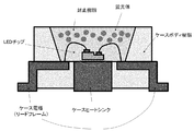
- the cross-sectional schematic diagram of the LED package of this invention is shown.
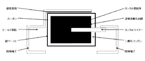
- the cross-sectional schematic diagram of the tantalum capacitor of this invention is shown.
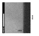
- the TEM image of the outermost layer of Example 4 is shown.
- concentration profile of EDS in the outermost surface layer of 10 nm of the said surface obtained by STEM of Example 4 is shown.
- the metal material according to the present invention is a metal material having a surface for bonding with a liquid crystal polymer, and EDS (energy dispersive X-ray analysis) within 10 nm of the outermost layer of the surface obtained by STEM (scanning electron microscope).
- EDS energy dispersive X-ray analysis
- the thickness of any one of Si, Ti, Al, Zr, Sn, Mg, and Ce is 1 nm or more.
- the metal material according to the present invention is not particularly limited as long as it has such a surface.
- the metal material may have any of the following configurations (1) to (5).
- Metal substrate + Metal substrate oxide layer + Coupling agent layer (2) Metal substrate + Plating layer + Coupling agent layer (3) Metal substrate + Plating layer + Plating layer oxide layer + Coupling agent layer (4) Metal substrate + Metal substrate oxide layer + Plating layer + Coupling agent layer (5) Metal substrate + Metal substrate oxide layer + Plating layer + Plating layer oxide layer + Coupling agent layer
- a plating layer and / or a coupling agent layer may be directly formed on the metal substrate as in the configurations shown in (1) to (5). After the oxide layer is formed by oxidation of the metal substrate, a plating layer and / or a coupling agent layer may be formed. In addition, a coupling agent layer may be formed directly on the plating layer, or after the oxide layer is formed by oxidation of the plating layer, the coupling agent layer may be formed.
- metal base material For example, copper, titanium, a copper alloy, or a titanium alloy etc. are mentioned. Among these, copper or a copper alloy has the advantages of high conductivity, excellent spreadability, and good spring characteristics.
- the silver layer, silver alloy layer with white Ni, Sn, In, etc. like silver, the multilayer structure of Ag layer and another metal layer, or an alloy layer etc. are mentioned, for example. It is done.
- the coupling agent layer is a silane coupling agent containing nitrogen in the molecule, titanate coupling agent, aluminate coupling agent, zirconia coupling agent, magnesium coupling agent, tin coupling agent, cerium coupling agent, etc. It is formed by surface treatment on a metal material.
- the metal material of the present invention has a surface for bonding with a liquid crystal polymer, and in the concentration profile of EDS within the outermost layer of 10 nm of the surface obtained by STEM, Si, Ti, Al, Zr, Sn, Mg, Ce
- the thickness of any layer is 1 nm or more.
- the thickness in the present invention is a width that is half of the maximum value of the concentration profile of EDS. According to such a configuration, sufficient adhesion between the metal material and the LCP is ensured. Although the cause of the improvement in adhesion is not clear, it is estimated that a small amount of Si, Ti, Al, Zr, Sn, Mg, Ce is present on the surface layer of the metal material, so that the bond with LCP is strengthened. .
- Si, Ti, Al, Zr, Sn, Mg, and Ce are preferably central elements of the coupling agent.
- the present inventors have found that more of these elements can be present on the surface of a metal material if the coupling agent contains N.
- the coupling agent containing N for example, in the case of a silane coupling agent, an aminosilane coupling agent, an isocyanate coupling agent, a ureidosilane coupling agent, and an imidazolesilane coupling agent.
- an aminosilane coupling agent that is inexpensive and easy to procure is preferable.
- the coupling agent Since the coupling agent has only a few layers on the surface of the metal material, it does not impair the properties such as high reflectivity and sulfidation resistance already imparted to the metal material by plating. When a layer of Si, Ti, Al, Zr, Sn, Mg, and Ce is formed on the surface of a metal material by wet or dry surface treatment, there is a high possibility that characteristics already imparted to the metal material are impaired. Further, according to the present invention, since the adhesion between the LCP and the metal material can be secured without performing the roughening treatment used for improving the adhesion between the copper foil and the insulating substrate, it is also advantageous from the viewpoint of the manufacturing process. There is.
- the background member is desirably white so that more light is reflected and brightened, that is, in order to increase the reflectance.
- the lead frame material is plated with silver to increase the reflectivity. Since the lead frame material is required to have sulfidation resistance in addition to the reflectance, the surface of the metal material is optimized from various viewpoints such as alloying the plating layer or multilayering. By performing silane treatment on the already optimized surface in this way, the metal material of the present invention can be produced, and the adhesion to the liquid crystal polymer is improved while maintaining the properties imparted to the metal material. be able to. Moreover, in the EDS concentration profile within 10 nm of the outermost surface layer obtained by STEM, the thickness of any one of Si, Ti, Al, Zr, Sn, Mg, and Ce is preferably 1.5 nm or more. .
- the metal material according to the present invention includes one or more metals selected from Cu, Al, Cr, Ag, Ni, In, and Sn below Si, Ti, Al, Zr, Sn, Mg, and Ce on the surface. It preferably has an oxide layer. According to such a configuration, sufficient adhesion between the metal material and the LCP is ensured.
- Si, Ti, Al, Zr, Sn, Mg, and Ce are preferably central elements of the coupling agent.
- N is preferably a functional group of the coupling agent.
- the coupling agent containing N for example, in the case of a silane coupling agent, an aminosilane coupling agent, an isocyanate coupling agent, a ureidosilane coupling agent, and an imidazolesilane coupling agent.
- an aminosilane coupling agent that is inexpensive and easy to procure is preferable. Since the coupling agent has only a few layers on the surface of the metal material, it does not impair the properties such as high reflectivity and sulfidation resistance already imparted to the metal material by plating. Further, according to the present invention, since the adhesion between the LCP and the metal material can be secured without performing the roughening treatment used for improving the adhesion between the copper foil and the insulating substrate, it is also advantageous from the viewpoint of the manufacturing process. There is.
- the metal-liquid crystal polymer composite of the present invention is constituted by bonding a liquid crystal polymer to the surface of the metal material of the present invention.
- the liquid crystal polymer is an aromatic polyester-based resin based on parahydroxybenzoic acid or the like and linearly ester-bonded with various components. It exhibits liquid crystal-like properties in which molecular straight chains are regularly arranged in the molten state.
- an inorganic filler may be dispersed.
- the liquid crystal polymer usually does not have good adhesion to a metal material, but surprisingly, when a destructive test is performed by joining with a metal material having a characteristic surface of the present invention, the liquid crystal polymer / The more the fracture occurs inside the liquid crystal polymer, not at the metal interface, the better the adhesion of the liquid crystal polymer / metal interface.
- Metal-liquid crystal polymer composite is a silane coupling agent, titanate coupling agent, aluminate coupling agent, zirconia coupling agent, magnesium coupling agent, tin coupling agent, cerium coupling agent containing nitrogen in the molecule.
- the metal material of the present invention is subjected to a surface treatment, and a liquid crystal polymer is bonded to the treated surface of the metal material by pressure bonding or injection molding.
- the electronic component of the present invention is not particularly limited as long as it includes the metal-liquid crystal polymer composite of the present invention, and examples thereof include an LED package and a capacitor.
- the case where the electronic component of the present invention is an LED package will be described.
- FIG. 1 the cross-sectional schematic diagram of the LED package of this invention is shown.
- the LED package is a lead frame in which the metal material of the present invention is white-plated, and the surface of the metal material to be bonded to the liquid crystal polymer is treated with a coupling agent having nitrogen in the molecule on the white-plated surface of the lead frame.
- the lead frame is used as a case electrode, the LED chip is mounted on the case electrode, the chip is covered with a case body made of a liquid crystal polymer, and a sealing resin containing a phosphor is contained in the case body. It is configured by filling. With such a configuration, in the LED package of the present invention, the lead frame is bonded to the liquid crystal polymer with good adhesion.
- the electronic component of the present invention is a capacitor of any one of aluminum, tantalum and niobium.
- the case where the electronic component of the present invention is a tantalum capacitor will be described.
- FIG. 2 shows a schematic cross-sectional view of the tantalum capacitor of the present invention.
- the tantalum capacitor is a part or all of a capacitor body in which the metal material of the present invention is covered with a cathode terminal, an anode terminal, and an outermost layer with a metal paste, and the cathode terminal, the anode terminal, and the capacitor body are liquid crystals. Consists of covered with polymer. With such a configuration, in the tantalum capacitor of the present invention, the cathode terminal, the anode terminal, and the capacitor body are bonded to the liquid crystal polymer with good adhesion.
- the liquid crystal polymer preferably has a difference in coefficient of thermal expansion of ⁇ 10 ppm / ° C. from the metal material. According to such a configuration, when heat is applied to the metal-liquid crystal polymer composite in which the metal material and the liquid crystal polymer are joined, the difference in thermal expansion coefficient between the two is small. It is suppressed.
- the difference in thermal expansion coefficient between the liquid crystal polymer and the metal material is more preferably ⁇ 5 ppm / ° C.
- Example 1 Examples 4 to 6, 9 to 11] (Silane solution adjustment) Collect 10 mL each of N- (2-aminoethyl) -3-aminopropyltrimethoxysilane, 3-aminopropyltriethoxysilane, 3-isocyanatopropyltriethoxysilane, and 3-ureidopropyltriethoxysilane (Momentive). Pure water was added to prepare 1 L aqueous solution.
- a liquid crystal polymer film (Kexar CT-Z manufactured by Kuraray Co., Ltd.) was laminated on the surface-treated surface (laminated up to 295 ° C. at a rate of 7 ° C./min and held at 295 ° C. for 1 hour) to prepare a metal-resin laminate. .
- the resin side of this laminate was peeled off, and the peel strength was measured according to the 180 ° peeling method (JIS C 6471 8.1).
- the thickness (nm) of the surface treatment layer of the surface-treated plate material was analyzed by EDS under the following conditions.
- Example 2 Examples 1 and 2] 10 mL of N- (2-aminoethyl) -3-aminopropyltrimethoxysilane (made by Momentive) was sampled, pure water was added, pH was adjusted with acetic acid, and 1 L aqueous solution of two types of pH was prepared. Using this silane solution, a 1 ⁇ m thick Ag-plated copper plate was subjected to surface treatment according to the procedure of Example 1, and various evaluations were performed.
- Example 3 Examples 7 and 8] 10 mL of N- (2-aminoethyl) -3-aminopropyltrimethoxysilane (manufactured by Momentive) was collected and 1 L of an aqueous solution was prepared by adding pure water. Using this, surface treatment was performed on the copper plate and the aluminum plate in the procedure of Example 1, and various evaluations were performed.
- Example 4 Titanate coupling agent having an amino group 10 mL of Preneact KR44 (manufactured by Ajinomoto Fine Techno Co., Ltd.) was collected, and 1 L of an aqueous solution was prepared by adding pure water. Surface treatment was performed on a 1 ⁇ m thick Ag-plated copper plate in the procedure of Example 1, and various evaluations were performed.
- Preneact KR44 manufactured by Ajinomoto Fine Techno Co., Ltd.
- Example 5 Comparative Example 1
- 10 mL of 3-glycidoxypropyltriethoxysilane manufactured by Momentive
- pure water was added
- the pH was adjusted to 3 with acetic acid
- a 1 L aqueous solution was prepared.
- surface treatment was performed on a 1 ⁇ m thick Ag-plated copper plate in the procedure of Example 1, and various evaluations were performed.
- Example 6 Comparative Example 2
- 10 mL of vinyltriethoxysilane manufactured by Momentive
- pure water was added to prepare a 1 L aqueous solution.
- surface treatment was performed on a 1 ⁇ m thick Ag-plated copper plate in the procedure of Example 1, and various evaluations were performed.
- Example 7 Comparative Example 3
- 10 g of 1,2,3-benzotriazole manufactured by Nacalai Tesque
- pure water was added to prepare a 1 L aqueous solution.
- surface treatment was performed on a 1 ⁇ m thick Ag-plated copper plate in the procedure of Example 1, and various evaluations were performed.
- Example 8 Comparative Example 4
- Various evaluations were performed according to the procedure of Example 1 using a 1 ⁇ m-thick Ag-plated copper plate. Table 1 shows test conditions and evaluation results of Examples and Comparative Examples.
- the adhesion surface with the resin is roughened, the physical effect is secured by the anchor effect, and the adhesion between the copper foil and the resin is further improved by the interaction between the silane coupling agent and the resin.
- the roughening treatment is not performed at a thickness (0.3 nm) of Comparative Examples 1 and 2 formed by the conventional silane treatment. It can be seen from the result of 1 that it cannot be handled.
- aminosilane has a feature that a thick layer of about 1 nm can be formed by silane treatment. In the present invention, such characteristics affect the good adhesion to the liquid crystal polymer.
- the coupling agent containing an amino group, a ureido group and an isocyanate group is not the same coupling agent used in the examples. However, it is estimated that it adheres in an amount sufficient to give the same effect to the surface of the metal material.
- FIG. 3 the TEM image of the outermost layer of Example 4 is shown.
- FIG. 4 shows a concentration profile of EDS within 10 nm of the outermost surface layer obtained by the STEM of Example 4.
Landscapes
- Engineering & Computer Science (AREA)
- Power Engineering (AREA)
- Chemical & Material Sciences (AREA)
- Microelectronics & Electronic Packaging (AREA)
- Organic Chemistry (AREA)
- Chemical Kinetics & Catalysis (AREA)
- Materials Engineering (AREA)
- Mechanical Engineering (AREA)
- Metallurgy (AREA)
- Manufacturing & Machinery (AREA)
- Led Device Packages (AREA)
- Laminated Bodies (AREA)
- Other Surface Treatments For Metallic Materials (AREA)
- Structures Or Materials For Encapsulating Or Coating Semiconductor Devices Or Solid State Devices (AREA)
- Conductive Materials (AREA)
Abstract
液晶ポリマーと良好な密着力で接合する表面を有する金属材料、金属-液晶ポリマー複合体及びその製造方法、並びに、電子部品を提供する。液晶ポリマーと接合させるための表面を有する金属材料であり、STEMで得られる前記表面の最表層10nm以内におけるEDS(エネルギー分散型X線分析)の濃度プロファイルにおいて、Si、Ti、Al、Zr、Sn、Mg、Ceのいずれかの層の厚みが1nm以上である金属材料。
Description
本発明は、液晶ポリマーと接合させるための表面を有する金属材料、金属-液晶ポリマー複合体及びその製造方法、並びに、電子部品に関する。
近年、省エネ、低コスト化の観点からLEDの普及が進行している。LEDの発光素子から放たれる光を最大限利用するために、素子を搭載する電極にはAgを主成分とした白色めっきが施されている。耐硫化性や低コスト化の観点から純AgめっきではなくInやSnをはじめとした合金めっきが開発されている。
また、LED素子を封止材で封止するために形成されるボディケースは高耐熱性のナイロンを射出成形して形成される。このボディケース用の樹脂としては例えば芳香族ポリアミドのアモデル(登録商標)がある。
また、電子機器で取り扱う信号は高周波数帯であることが多く、例えば、タンタルコンデンサは電源平滑用やノイズ除去のバイパスコンデンサとして用いられる。このタンタルコンデンサは陰極端子、陽極端子、及び、Agペーストで覆われたコンデンサ本体をエポキシ樹脂で覆うことで構成されている。タンタルコンデンサでは誘電率が高い酸化タンタルが誘電体として用いられている。さらに、最近では酸化タンタルよりも誘電率が高い酸化ニオブを誘電体としたニオブコンデンサが注目を集めている。
また、LED素子を封止材で封止するために形成されるボディケースは高耐熱性のナイロンを射出成形して形成される。このボディケース用の樹脂としては例えば芳香族ポリアミドのアモデル(登録商標)がある。
また、電子機器で取り扱う信号は高周波数帯であることが多く、例えば、タンタルコンデンサは電源平滑用やノイズ除去のバイパスコンデンサとして用いられる。このタンタルコンデンサは陰極端子、陽極端子、及び、Agペーストで覆われたコンデンサ本体をエポキシ樹脂で覆うことで構成されている。タンタルコンデンサでは誘電率が高い酸化タンタルが誘電体として用いられている。さらに、最近では酸化タンタルよりも誘電率が高い酸化ニオブを誘電体としたニオブコンデンサが注目を集めている。
このような技術として、例えば、特許文献1には、高反射率に加え、製造性に優れたLED用リードフレームの表面処理技術が開示されている。また、特許文献2にはエポキシ樹脂を封止剤としたタンタルコンデンサが、特許文献3にはニオブコンデンサが開示されている。
LEDのケースボディで使用されるアモデルに代表される芳香族ポリアミドは、流動性に劣り、ケースボディの射出成形に問題があった。これに対し、本発明者は、芳香族ポリアミドを液晶ポリマーに代えると流動性が増すため、ケースボディの射出成形が容易になることを見出した。また、液晶ポリマー自体が白いので、白色の電極とあわせてよりLED素子の白色光をより効率よく放つことが可能となる。
また、タンタルコンデンサのカバーに使用されているエポキシ樹脂は硬化剤を混ぜ合わせなければならないので、樹脂の調合工程が必要であるが、このエポキシ樹脂を液晶ポリマーとすれば、調合工程を省くことが可能となる。
一方、Agめっきをはじめとした白色めっきをした電極に液晶ポリマーを射出成形すると、電極表面と液晶ポリマーの密着性が低いためか、隙間ができてしまい、このようなケースボディに封止樹脂を充填しても隙間から封止樹脂が漏れてしまう問題を発見した。
本発明は上記の課題を解決するためになされたものであり、液晶ポリマーと良好な密着力で接合する表面を有する金属材料、金属-液晶ポリマー複合体及びその製造方法、並びに、電子部品を提供することを課題とする。
また、タンタルコンデンサのカバーに使用されているエポキシ樹脂は硬化剤を混ぜ合わせなければならないので、樹脂の調合工程が必要であるが、このエポキシ樹脂を液晶ポリマーとすれば、調合工程を省くことが可能となる。
一方、Agめっきをはじめとした白色めっきをした電極に液晶ポリマーを射出成形すると、電極表面と液晶ポリマーの密着性が低いためか、隙間ができてしまい、このようなケースボディに封止樹脂を充填しても隙間から封止樹脂が漏れてしまう問題を発見した。
本発明は上記の課題を解決するためになされたものであり、液晶ポリマーと良好な密着力で接合する表面を有する金属材料、金属-液晶ポリマー複合体及びその製造方法、並びに、電子部品を提供することを課題とする。
電極、端子の表面処理は、反射率、耐硫化性等、様々な特性に合わせて最適化されていることが多い。そこで、本発明者は、鋭意検討の結果、これらの表面処理を生かしつつ、液晶ポリマーとの密着力を向上させる手段として、金属側をカップリング剤処理することに着目した。
カップリング剤の主成分元素としてはSi、Ti、Zr、Al、Sn、Ceがあるが、安定性の観点から、Si、Tiが望ましい。また、分子内に窒素を含む官能基を有していると、金属材料の、液晶ポリマーとの密着力が向上することを見出した。
カップリング剤の主成分元素としてはSi、Ti、Zr、Al、Sn、Ceがあるが、安定性の観点から、Si、Tiが望ましい。また、分子内に窒素を含む官能基を有していると、金属材料の、液晶ポリマーとの密着力が向上することを見出した。
以上の知見を基礎として完成した本発明は一側面において、液晶ポリマーと接合させるための表面を有する金属材料であり、STEM(走査型電子顕微鏡)で得られる前記表面の最表層10nm以内におけるEDS(エネルギー分散型X線分析)の濃度プロファイルにおいて、Si、Ti、Al、Zr、Sn、Mg、Ceのいずれかの層の厚みが1nm以上である金属材料である。
本発明に係る金属材料は一実施形態において、STEM(走査型電子顕微鏡)で得られる前記表面の最表層10nm以内におけるEDS(エネルギー分散型X線分析)の濃度プロファイルにおいて、Si、Ti、Al、Zr、Sn、Mg、Ceのいずれかの層の厚みが1.5nm以上である。
本発明に係る金属材料は別の一実施形態において、前記表面のSi、Ti、Al、Zr、Sn、Mg、Ceの下方に、Cu、Al、Cr、Ag、Ni、In、Snのいずれか1種以上の金属又はその酸化物の層を有する。
本発明は別の一側面において、本発明の金属材料の前記表面に液晶ポリマーが接合されてなる金属-液晶ポリマー複合体である。
本発明は更に別の一側面において、窒素を分子内に含有するシランカップリング剤、チタネートカップリング剤、アルミネートカップリング剤、ジルコニアカップリング剤、マグネシウムカップリング剤、スズカップリング剤、セリウムカップリング剤のいずれかで金属材料に表面処理を施し、前記金属材料の処理面に液晶ポリマーを圧着又は射出成形で接合させる、金属-液晶ポリマー複合体の製造方法である。
本発明は更に別の一側面において、本発明の金属-液晶ポリマー複合体を備えた電子部品である。
本発明に係る電子部品は一実施形態において、前記金属材料が白色めっきをしたリードフレームであり、液晶ポリマーと接合させるための前記金属材料の表面が、前記リードフレームの白色めっき表面に窒素を分子内に有するカップリング剤処理で形成されており、前記リードフレームをケース電極とし、前記ケース電極上にLEDチップが実装され、前記チップが周辺を前記液晶ポリマーからなるケースボディで覆われ、前記ケースボディ内に蛍光体を含有する封止樹脂が充填されることで構成されたLEDパッケージである。
本発明に係る電子部品は別の一実施形態において、前記金属材料が陰極端子、陽極端子、及び、最表層が金属ペーストで覆われたコンデンサ本体の一部または全部であり、前記陰極端子、前記陽極端子、及び、前記コンデンサ本体が液晶ポリマーで覆われて構成された、アルミ、タンタル及びニオブのうちいずれかのコデンサである。
本発明に係る電子部品は更に別の一実施形態において、前記液晶ポリマーは、前記金属材料との熱膨張係数の差が±10ppm/℃である。
本発明によれば、液晶ポリマーと良好な密着力で接合する表面を有する金属材料、金属-液晶ポリマー複合体及びその製造方法、並びに、電子部品を提供することができる。また、本発明によれば、銅箔と絶縁基板との密着力向上に利用される粗面化処理を行うことなく、LCPと金属材料の密着力を確保できるので、製造工程の観点からもメリットがある。
(金属材料)
本発明に係る金属材料は、液晶ポリマーと接合させるための表面を有する金属材料であり、STEM(走査型電子顕微鏡)で得られる前記表面の最表層10nm以内におけるEDS(エネルギー分散型X線分析)の濃度プロファイルにおいて、Si、Ti、Al、Zr、Sn、Mg、Ceのいずれかの層の厚みが1nm以上である。本発明に係る金属材料はこのような表面を有していれば特に限定されないが、例えば、以下の(1)~(5)で示す構成のいずれかであってもよい。
(1)金属基材+金属基材の酸化物層+カップリング剤層
(2)金属基材+めっき層+カップリング剤層
(3)金属基材+めっき層+めっき層の酸化物層+カップリング剤層
(4)金属基材+金属基材の酸化物層+めっき層+カップリング剤層
(5)金属基材+金属基材の酸化物層+めっき層+めっき層の酸化物層+カップリング剤層
本発明に係る金属材料は、液晶ポリマーと接合させるための表面を有する金属材料であり、STEM(走査型電子顕微鏡)で得られる前記表面の最表層10nm以内におけるEDS(エネルギー分散型X線分析)の濃度プロファイルにおいて、Si、Ti、Al、Zr、Sn、Mg、Ceのいずれかの層の厚みが1nm以上である。本発明に係る金属材料はこのような表面を有していれば特に限定されないが、例えば、以下の(1)~(5)で示す構成のいずれかであってもよい。
(1)金属基材+金属基材の酸化物層+カップリング剤層
(2)金属基材+めっき層+カップリング剤層
(3)金属基材+めっき層+めっき層の酸化物層+カップリング剤層
(4)金属基材+金属基材の酸化物層+めっき層+カップリング剤層
(5)金属基材+金属基材の酸化物層+めっき層+めっき層の酸化物層+カップリング剤層
すなわち、本発明に係る金属材料は、(1)~(5)で示す構成のように、金属基材上には、直接、めっき層及び/又はカップリング剤層が形成されていてもよく、金属基材の酸化により酸化物層が形成された後に、めっき層及び/又はカップリング剤層が形成されていてもよい。また、めっき層上には、直接カップリング剤層が形成されていてもよく、めっき層の酸化により酸化物層が形成された後に、カップリング剤層が形成されていてもよい。
金属基材としては、特に限定されないが、例えば、銅、チタン、銅合金又はチタン合金等が挙げられる。このうち、銅又は銅合金は、導電性が高い、展延性に富む、及び、ばね特性が良好という利点を有する。
めっき層としては、特に限定されないが、例えば、銀層、銀と同じく白色のNiやSnやIn等との銀合金層、Ag層と別の金属層または合金層との複層構造等が挙げられる。
カップリング剤層は、窒素を分子内に含有するシランカップリング剤、チタネートカップリング剤、アルミネートカップリング剤、ジルコニアカップリング剤、マグネシウムカップリング剤、スズカップリング剤、セリウムカップリング剤等で金属材料に表面処理することで形成される。
本発明の金属材料は、液晶ポリマーと接合させるための表面を有しSTEMで得られる前記表面の最表層10nm以内におけるEDSの濃度プロファイルにおいて、Si、Ti、Al、Zr、Sn、Mg、Ceのいずれかの層の厚みが1nm以上である。本発明における厚みとは、EDSの濃度プロファイルの最大値の半分となる幅である。
このような構成によれば、金属材料とLCPとの密着力が十分に確保される。密着性が向上する要因は明らかではないが、少量のSi、Ti、Al、Zr、Sn、Mg、Ceが金属材料の表層に存在することで、LCPとの結合が強まっていると推定される。Si、Ti、Al、Zr、Sn、Mg、Ceはカップリング剤の中心元素であるのが好ましい。特に、Nを含有するカップリング剤であれば、より多くのこれらの元素が金属材料表面に存在できることを本発明者は見出した。Nを含有するカップリング剤としては、例えばシランカップリング剤であれば、アミノシランカップリング剤、イソシアネートカップリング剤、ウレイドシランカップリング剤、イミダゾールシランカップリング剤である。特に安価で調達が容易なアミノシランカップリング剤が好ましい。カップリング剤であれば金属材料表面には高々数層しか存在しないので、すでにめっきで金属材料に付与された高反射率、耐硫化性等の特性を損なうことはない。Si、Ti、Al、Zr、Sn、Mg、Ceの層を湿式または乾式の表面処理で金属材料表面に形成すると、すでに金属材料に付与されている特性を損なう可能性が高い。また、本発明によれば、銅箔と絶縁基板との密着力向上に利用される粗面化処理を行うことなく、LCPと金属材料の密着力を確保できるので、製造工程の観点からもメリットがある。
例えば、LEDのリードフレーム材用の金属材料の場合、より多くの光が反射して明るくなるように、すなわち反射率を高くするために、背景の部材は白いことが望ましい。リードフレーム材ではこの反射率を上げるために銀系のめっきが施される。このリードフレーム材は反射率に加えて耐硫化性も求められるため、めっき層を合金化する、或いは複層化する等、種々の観点から金属材料表面が最適化されている。このように既に最適化された表面にシラン処理を行うことで、本発明の金属材料を作製することができ、金属材料に付与された特性を維持したまま、液晶ポリマーとの密着力を向上させることができる。
また、STEMで得られる前記表面の最表層10nm以内におけるEDSの濃度プロファイルにおいて、Si、Ti、Al、Zr、Sn、Mg、Ceのいずれかの層の厚みが1.5nm以上であるのが好ましい。
このような構成によれば、金属材料とLCPとの密着力が十分に確保される。密着性が向上する要因は明らかではないが、少量のSi、Ti、Al、Zr、Sn、Mg、Ceが金属材料の表層に存在することで、LCPとの結合が強まっていると推定される。Si、Ti、Al、Zr、Sn、Mg、Ceはカップリング剤の中心元素であるのが好ましい。特に、Nを含有するカップリング剤であれば、より多くのこれらの元素が金属材料表面に存在できることを本発明者は見出した。Nを含有するカップリング剤としては、例えばシランカップリング剤であれば、アミノシランカップリング剤、イソシアネートカップリング剤、ウレイドシランカップリング剤、イミダゾールシランカップリング剤である。特に安価で調達が容易なアミノシランカップリング剤が好ましい。カップリング剤であれば金属材料表面には高々数層しか存在しないので、すでにめっきで金属材料に付与された高反射率、耐硫化性等の特性を損なうことはない。Si、Ti、Al、Zr、Sn、Mg、Ceの層を湿式または乾式の表面処理で金属材料表面に形成すると、すでに金属材料に付与されている特性を損なう可能性が高い。また、本発明によれば、銅箔と絶縁基板との密着力向上に利用される粗面化処理を行うことなく、LCPと金属材料の密着力を確保できるので、製造工程の観点からもメリットがある。
例えば、LEDのリードフレーム材用の金属材料の場合、より多くの光が反射して明るくなるように、すなわち反射率を高くするために、背景の部材は白いことが望ましい。リードフレーム材ではこの反射率を上げるために銀系のめっきが施される。このリードフレーム材は反射率に加えて耐硫化性も求められるため、めっき層を合金化する、或いは複層化する等、種々の観点から金属材料表面が最適化されている。このように既に最適化された表面にシラン処理を行うことで、本発明の金属材料を作製することができ、金属材料に付与された特性を維持したまま、液晶ポリマーとの密着力を向上させることができる。
また、STEMで得られる前記表面の最表層10nm以内におけるEDSの濃度プロファイルにおいて、Si、Ti、Al、Zr、Sn、Mg、Ceのいずれかの層の厚みが1.5nm以上であるのが好ましい。
本発明の金属材料は、前記表面のSi、Ti、Al、Zr、Sn、Mg、Ceの下方に、Cu、Al、Cr、Ag、Ni、In、Snのいずれか1種以上の金属又はその酸化物の層を有するのが好ましい。
このような構成によれば、金属材料とLCPとの密着力が十分に確保される。Si、Ti、Al、Zr、Sn、Mg、Ceはカップリング剤の中心元素であるのが好ましい。Nはカップリング剤の官能基であるのが好ましい。Nを含有するカップリング剤としては、例えばシランカップリング剤であれば、アミノシランカップリング剤、イソシアネートカップリング剤、ウレイドシランカップリング剤、イミダゾールシランカップリング剤である。特に安価で調達が容易なアミノシランカップリング剤が好ましい。カップリング剤であれば金属材料表面には高々数層しか存在しないので、すでにめっきで金属材料に付与された高反射率、耐硫化性等の特性を損なうことはない。また、本発明によれば、銅箔と絶縁基板との密着力向上に利用される粗面化処理を行うことなく、LCPと金属材料の密着力を確保できるので、製造工程の観点からもメリットがある。
このような構成によれば、金属材料とLCPとの密着力が十分に確保される。Si、Ti、Al、Zr、Sn、Mg、Ceはカップリング剤の中心元素であるのが好ましい。Nはカップリング剤の官能基であるのが好ましい。Nを含有するカップリング剤としては、例えばシランカップリング剤であれば、アミノシランカップリング剤、イソシアネートカップリング剤、ウレイドシランカップリング剤、イミダゾールシランカップリング剤である。特に安価で調達が容易なアミノシランカップリング剤が好ましい。カップリング剤であれば金属材料表面には高々数層しか存在しないので、すでにめっきで金属材料に付与された高反射率、耐硫化性等の特性を損なうことはない。また、本発明によれば、銅箔と絶縁基板との密着力向上に利用される粗面化処理を行うことなく、LCPと金属材料の密着力を確保できるので、製造工程の観点からもメリットがある。
(金属-液晶ポリマー複合体)
本発明の金属-液晶ポリマー複合体は、本発明の金属材料の前記表面に液晶ポリマーが接合されて構成されている。液晶ポリマーは、パラヒドロキシ安息香酸などを基本とし、各種の成分と直鎖状にエステル結合させた芳香族ポリエステル系樹脂である。溶融状態で分子の直鎖が規則正しく並んだ液晶様性質を示す。諸特性、例えば熱膨張係数を制御するために、無機フィラーを分散させることがある。
液晶ポリマーは、通常、金属材料との密着性が良くないが、本発明の特徴的な表面を有する金属材料と接合させることで、破壊試験を行った場合等、驚くべきことに、液晶ポリマー/金属界面の破壊ではなく、液晶ポリマーの内部で破壊が起きるほど、液晶ポリマー/金属界面の密着力が向上する。
本発明の金属-液晶ポリマー複合体は、本発明の金属材料の前記表面に液晶ポリマーが接合されて構成されている。液晶ポリマーは、パラヒドロキシ安息香酸などを基本とし、各種の成分と直鎖状にエステル結合させた芳香族ポリエステル系樹脂である。溶融状態で分子の直鎖が規則正しく並んだ液晶様性質を示す。諸特性、例えば熱膨張係数を制御するために、無機フィラーを分散させることがある。
液晶ポリマーは、通常、金属材料との密着性が良くないが、本発明の特徴的な表面を有する金属材料と接合させることで、破壊試験を行った場合等、驚くべきことに、液晶ポリマー/金属界面の破壊ではなく、液晶ポリマーの内部で破壊が起きるほど、液晶ポリマー/金属界面の密着力が向上する。
金属-液晶ポリマー複合体は、窒素を分子内に含有するシランカップリング剤、チタネートカップリング剤、アルミネートカップリング剤、ジルコニアカップリング剤、マグネシウムカップリング剤、スズカップリング剤、セリウムカップリング剤のいずれかで本発明の金属材料に表面処理を施し、金属材料の前記処理面に液晶ポリマーを圧着又は射出成形で接合させることで作製することができる。
(電子部品)
本発明の電子部品は、本発明の金属-液晶ポリマー複合体を備えていればよく、特に限定されないが、LEDパッケージやコンデンサ等が挙げられる。
本発明の電子部品がLEDパッケージである場合について説明する。図1に、本発明のLEDパッケージの断面模式図を示す。当該LEDパッケージは、本発明の金属材料が白色めっきをしたリードフレームであり、液晶ポリマーと接合させるための金属材料の表面が、リードフレームの白色めっき表面に窒素を分子内に有するカップリング剤処理で形成されており、リードフレームをケース電極とし、ケース電極上にLEDチップが実装され、チップが周辺を液晶ポリマーからなるケースボディで覆われ、ケースボディ内に蛍光体を含有する封止樹脂が充填されることで構成されている。このような構成により、本発明のLEDパッケージは、リードフレームが液晶ポリマーと良好な密着力で接合されている。
本発明の電子部品は、本発明の金属-液晶ポリマー複合体を備えていればよく、特に限定されないが、LEDパッケージやコンデンサ等が挙げられる。
本発明の電子部品がLEDパッケージである場合について説明する。図1に、本発明のLEDパッケージの断面模式図を示す。当該LEDパッケージは、本発明の金属材料が白色めっきをしたリードフレームであり、液晶ポリマーと接合させるための金属材料の表面が、リードフレームの白色めっき表面に窒素を分子内に有するカップリング剤処理で形成されており、リードフレームをケース電極とし、ケース電極上にLEDチップが実装され、チップが周辺を液晶ポリマーからなるケースボディで覆われ、ケースボディ内に蛍光体を含有する封止樹脂が充填されることで構成されている。このような構成により、本発明のLEDパッケージは、リードフレームが液晶ポリマーと良好な密着力で接合されている。
本発明の電子部品は、アルミ、タンタル及びニオブのうちいずれかのコンデンサである。ここで、本発明の電子部品がタンタルコンデンサである場合について説明する。図2に、本発明のタンタルコンデンサの断面模式図を示す。当該タンタルコンデンサは、本発明の金属材料が陰極端子、陽極端子、及び、最表層が金属ペーストで覆われたコンデンサ本体の一部または全部であり、陰極端子、陽極端子、及び、コンデンサ本体が液晶ポリマーで覆われて構成されている。このような構成により、本発明のタンタルコンデンサは、陰極端子、陽極端子、及び、コンデンサ本体が液晶ポリマーと良好な密着力で接合されている。
本発明の電子部品において、液晶ポリマーは、金属材料との熱膨張係数の差が±10ppm/℃であるのが好ましい。このような構成によれば、金属材料と液晶ポリマーとが接合した金属-液晶ポリマー複合体に熱が加わった際、両者の熱膨張係数の差が小さいため、膨張による複合体の損傷が良好に抑制される。液晶ポリマーと金属材料との熱膨張係数の差は、より好ましくは±5ppm/℃である。
以下、本発明の実施例を示すが、これらは本発明をより良く理解するために提供するものであり、本発明が限定されることを意図するものではない。
〔例1:実施例4~6、9~11〕
(シラン溶液調整)
N-(2-アミノエチル)-3-アミノプロピルトリメトキシシラン、3-アミノプロピルトリエトキシシラン、3-イソシアネートプロピルトリエトキシシラン、3-ウレイドプロピルトリエトキシシラン(モメンティブ社製)をそれぞれ10mL採取し、純水を加えてそれぞれ1Lの水溶液を調整した。
(シラン溶液調整)
N-(2-アミノエチル)-3-アミノプロピルトリメトキシシラン、3-アミノプロピルトリエトキシシラン、3-イソシアネートプロピルトリエトキシシラン、3-ウレイドプロピルトリエトキシシラン(モメンティブ社製)をそれぞれ10mL採取し、純水を加えてそれぞれ1Lの水溶液を調整した。
(めっき板材へのシラン処理)
厚み0.1mmの銅板に1μmの厚みのAg、Ni、クロメートめっきをした。これらめっき銅板それぞれをアルカリ脱脂(NaOH:100g/L、30秒)、酸洗(H2SO4:10wt%、30秒)した後、上記シラン溶液に30秒浸漬させ、水洗し、乾燥させた。
厚み0.1mmの銅板に1μmの厚みのAg、Ni、クロメートめっきをした。これらめっき銅板それぞれをアルカリ脱脂(NaOH:100g/L、30秒)、酸洗(H2SO4:10wt%、30秒)した後、上記シラン溶液に30秒浸漬させ、水洗し、乾燥させた。
(液晶ポリマーとの密着力)
表面処理面に液晶ポリマーフィルム(クラレ社製 べクスターCT-Z)をラミネートで貼り合せ(295℃まで7℃/minで昇温、295℃で1時間保持)、金属-樹脂積層体を作製した。この積層体の樹脂側を引き剥がし、ピール強度を180°剥離法(JIS C 6471 8.1)に準拠して測定した。剥離後の金属側をSTEMで観察し、樹脂(LCP)が金属面に残っていれば「剥離はLCP内部」、金属面に残っていなければ「剥離はLCP表面」と判断した。
表面処理面に液晶ポリマーフィルム(クラレ社製 べクスターCT-Z)をラミネートで貼り合せ(295℃まで7℃/minで昇温、295℃で1時間保持)、金属-樹脂積層体を作製した。この積層体の樹脂側を引き剥がし、ピール強度を180°剥離法(JIS C 6471 8.1)に準拠して測定した。剥離後の金属側をSTEMで観察し、樹脂(LCP)が金属面に残っていれば「剥離はLCP内部」、金属面に残っていなければ「剥離はLCP表面」と判断した。
(めっき板材の表面分析〔STEMとEDSによる厚み算出〕)
表面処理された板材の表面処理層の厚み(nm)を、EDSによって、次の条件で分析した。
装置:STEM
断面TEM像倍率:4000000倍(400万倍)
特性X線
照射電子のビーム径:1nm
走査距離:100nm(銅粉の断面を走査)の5点平均
厚み定義:特性X線の深さ方向濃度プロファイルの最大値の50%となる領域。
表面処理された板材の表面処理層の厚み(nm)を、EDSによって、次の条件で分析した。
装置:STEM
断面TEM像倍率:4000000倍(400万倍)
特性X線
照射電子のビーム径:1nm
走査距離:100nm(銅粉の断面を走査)の5点平均
厚み定義:特性X線の深さ方向濃度プロファイルの最大値の50%となる領域。
(レッドインクテスト〔金属材料上に隙間なく液晶ポリマーの型が形成できているかの確認〕)
竪型射出成形機VH40(山城社製)を用いて表面処理をした板材上に液晶ポリマー(JX日鉱日石エネルギー社製 ザイダー)を、最高温度340℃、金型温度100℃、射出速度200mm/sで箱型に射出成形した。液晶ポリマーで形成された型内部に赤インク(ライオン事務器社製 スタンプインキ 赤)を垂らして、1日後、6日後にインクが型の外に漏れているかどうかを確認した。全くインクが漏れていない場合は「なし」、型の縁がにじんだ程度であれば「軽度のにじみ」、漏れていた場合は「あり」と判定した。
竪型射出成形機VH40(山城社製)を用いて表面処理をした板材上に液晶ポリマー(JX日鉱日石エネルギー社製 ザイダー)を、最高温度340℃、金型温度100℃、射出速度200mm/sで箱型に射出成形した。液晶ポリマーで形成された型内部に赤インク(ライオン事務器社製 スタンプインキ 赤)を垂らして、1日後、6日後にインクが型の外に漏れているかどうかを確認した。全くインクが漏れていない場合は「なし」、型の縁がにじんだ程度であれば「軽度のにじみ」、漏れていた場合は「あり」と判定した。
〔例2:実施例1、2〕
N-(2-アミノエチル)-3-アミノプロピルトリメトキシシラン(モメンティブ社製)を10mL採取し、純水を加えて、酢酸でpHを調整し、2種類のpHの1Lの水溶液を調整した。このシラン溶液を用いて厚み1μmのAgめっきをした銅板に例1の手順で表面処理を施し、各種評価を行った。
N-(2-アミノエチル)-3-アミノプロピルトリメトキシシラン(モメンティブ社製)を10mL採取し、純水を加えて、酢酸でpHを調整し、2種類のpHの1Lの水溶液を調整した。このシラン溶液を用いて厚み1μmのAgめっきをした銅板に例1の手順で表面処理を施し、各種評価を行った。
〔例3:実施例7、8〕
N-(2-アミノエチル)-3-アミノプロピルトリメトキシシラン(モメンティブ社製)を10mL採取し、純水を加えて1Lの水溶液を調整した。これを用いて、例1の手順で銅板、アルミ板に表面処理を施し、各種評価を行った。
N-(2-アミノエチル)-3-アミノプロピルトリメトキシシラン(モメンティブ社製)を10mL採取し、純水を加えて1Lの水溶液を調整した。これを用いて、例1の手順で銅板、アルミ板に表面処理を施し、各種評価を行った。
〔例4:実施例3〕
アミノ基を有するチタネートカップリング剤 プレンアクトKR44(味の素ファインテクノ社製)を10mL採取し、純水を加えて1Lの水溶液を調整した。例1の手順で1μm厚のAgめっきをした銅板に表面処理を施し、各種評価を行った。
アミノ基を有するチタネートカップリング剤 プレンアクトKR44(味の素ファインテクノ社製)を10mL採取し、純水を加えて1Lの水溶液を調整した。例1の手順で1μm厚のAgめっきをした銅板に表面処理を施し、各種評価を行った。
〔例5:比較例1〕
3-グリシドキシプロピルトリエトキシシラン(モメンティブ社製)を10mL採取し、純水を加えて、酢酸でpHを3に調整し、1Lの水溶液を調整した。これを用いて、例1の手順で1μm厚のAgめっきをした銅板に表面処理を施し、各種評価を行った。
3-グリシドキシプロピルトリエトキシシラン(モメンティブ社製)を10mL採取し、純水を加えて、酢酸でpHを3に調整し、1Lの水溶液を調整した。これを用いて、例1の手順で1μm厚のAgめっきをした銅板に表面処理を施し、各種評価を行った。
〔例6:比較例2〕
ビニルトリエトキシシラン(モメンティブ社製)を10mL採取し、純水を加えて、1Lの水溶液を調整した。これを用いて、例1の手順で1μm厚のAgめっきをした銅板に表面処理を施し、各種評価を行った。
ビニルトリエトキシシラン(モメンティブ社製)を10mL採取し、純水を加えて、1Lの水溶液を調整した。これを用いて、例1の手順で1μm厚のAgめっきをした銅板に表面処理を施し、各種評価を行った。
〔例7:比較例3〕
1,2,3-ベンゾトリアゾール(ナカライテスク社製)を10g採取し、純水を加えて、1Lの水溶液を調整した。これを用いて、例1の手順で1μm厚のAgめっきをした銅板に表面処理を施し、各種評価を行った。
1,2,3-ベンゾトリアゾール(ナカライテスク社製)を10g採取し、純水を加えて、1Lの水溶液を調整した。これを用いて、例1の手順で1μm厚のAgめっきをした銅板に表面処理を施し、各種評価を行った。
〔例8:比較例4〕
1μm厚のAgめっきをした銅板を用いて例1の手順で各種評価を行った。
実施例及び比較例の試験条件及び評価結果を表1に示す。
1μm厚のAgめっきをした銅板を用いて例1の手順で各種評価を行った。
実施例及び比較例の試験条件及び評価結果を表1に示す。
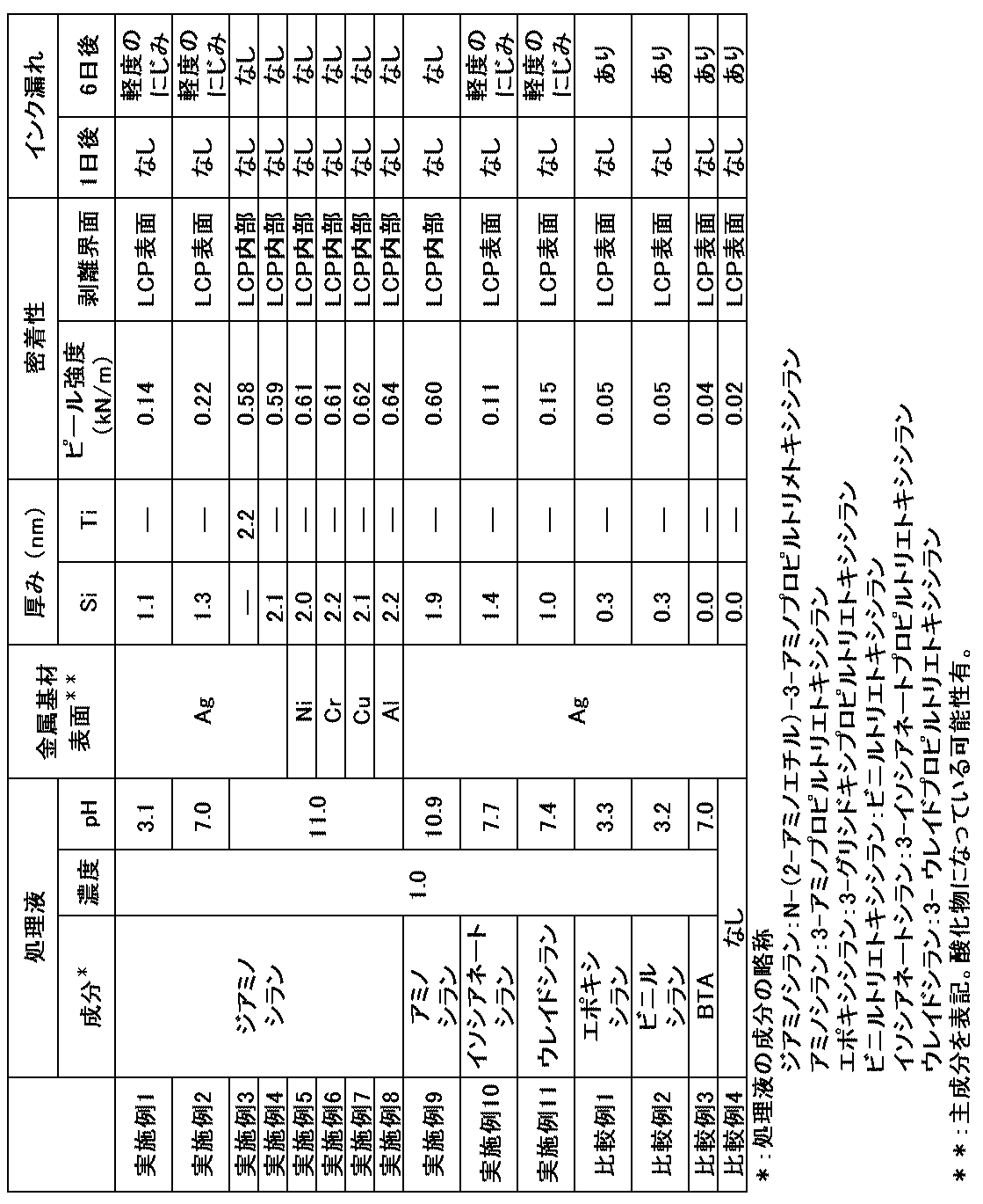
実施例1~11は、いずれも金属材料と液晶ポリマーとの密着力が良好であり、金属材料上に隙間なく液晶ポリマーの型が形成できていた。
比較例1~4は、STEMで得られる前記表面の最表層10nm以内におけるEDSの濃度プロファイルにおいて、Si、Ti、Al、Zr、Sn、Mg、Ceの層の厚みが1nm未満であったため、液晶ポリマーとの密着力が不良であり、金属材料と液晶ポリマーとの間に隙間が生じ、6日後にインク漏れが生じた。
プリント配線板の分野では、比較例1及び2程度の厚み(0.3nm)でも、ポリイミドをはじめとした液晶ポリマー以外の樹脂基板(絶縁基板)との密着性が改善される事例はあった。プリント配線板の分野では樹脂との密着面を粗化し、アンカー効果で物理的な効果を確保した上で、シランカップリング剤と樹脂との相互作用で銅箔と樹脂との密着力をさらに向上させる。しかしながら、本発明に係る液晶ポリマーとの接着性に関しては、従来のシラン処理で形成される比較例1及び2程度の厚み(0.3nm)では粗化処理をしていないこともあって、表1の結果から対応できないことがわかる。
また、アミノシランはそれ以外のシランと違って、シラン処理にしては厚い1nm前後の厚みの層を形成できるという特徴を有している。本発明ではこのような特徴が液晶ポリマーとの良好な接着性に影響を与えている。
さらに、実施例1~11で用いたカップリング剤とその評価結果から、アミノ基、ウレイド基、イソシアネート基を含むカップリング剤であれば、実施例で用いたものと同一のカップリング剤でなくても金属材料表面に同様の効果を与えるのに十分な量で付着すると推定される。
図3に、実施例4の最表層のTEM像を示す。図4に、実施例4のSTEMで得られる前記表面の最表層10nm以内におけるEDSの濃度プロファイルを示す。
以上のように本発明で形成される表面処理層は極薄なので、金属材料に既にめっき等で付与されている特性は維持されていると推定される。
比較例1~4は、STEMで得られる前記表面の最表層10nm以内におけるEDSの濃度プロファイルにおいて、Si、Ti、Al、Zr、Sn、Mg、Ceの層の厚みが1nm未満であったため、液晶ポリマーとの密着力が不良であり、金属材料と液晶ポリマーとの間に隙間が生じ、6日後にインク漏れが生じた。
プリント配線板の分野では、比較例1及び2程度の厚み(0.3nm)でも、ポリイミドをはじめとした液晶ポリマー以外の樹脂基板(絶縁基板)との密着性が改善される事例はあった。プリント配線板の分野では樹脂との密着面を粗化し、アンカー効果で物理的な効果を確保した上で、シランカップリング剤と樹脂との相互作用で銅箔と樹脂との密着力をさらに向上させる。しかしながら、本発明に係る液晶ポリマーとの接着性に関しては、従来のシラン処理で形成される比較例1及び2程度の厚み(0.3nm)では粗化処理をしていないこともあって、表1の結果から対応できないことがわかる。
また、アミノシランはそれ以外のシランと違って、シラン処理にしては厚い1nm前後の厚みの層を形成できるという特徴を有している。本発明ではこのような特徴が液晶ポリマーとの良好な接着性に影響を与えている。
さらに、実施例1~11で用いたカップリング剤とその評価結果から、アミノ基、ウレイド基、イソシアネート基を含むカップリング剤であれば、実施例で用いたものと同一のカップリング剤でなくても金属材料表面に同様の効果を与えるのに十分な量で付着すると推定される。
図3に、実施例4の最表層のTEM像を示す。図4に、実施例4のSTEMで得られる前記表面の最表層10nm以内におけるEDSの濃度プロファイルを示す。
以上のように本発明で形成される表面処理層は極薄なので、金属材料に既にめっき等で付与されている特性は維持されていると推定される。
Claims (9)
- 液晶ポリマーと接合させるための表面を有する金属材料であり、
STEMで得られる前記表面の最表層10nm以内におけるEDS(エネルギー分散型X線分析)の濃度プロファイルにおいて、Si、Ti、Al、Zr、Sn、Mg、Ceのいずれかの層の厚みが1nm以上である金属材料。 - STEMで得られる前記表面の最表層10nm以内におけるEDS(エネルギー分散型X線分析)の濃度プロファイルにおいて、Si、Ti、Al、Zr、Sn、Mg、Ceのいずれかの層の厚みが1.5nm以上である請求項1に記載の金属材料。
- 前記表面のSi、Ti、Al、Zr、Sn、Mg、Ceの下方に、Cu、Al、Cr、Ag、Ni、In、Snのいずれか1種以上の金属又はその酸化物の層を有する請求項1又は2に記載の金属材料。
- 請求項1~3のいずれかに記載の金属材料の前記表面に液晶ポリマーが接合されてなる金属-液晶ポリマー複合体。
- 窒素を分子内に含有するシランカップリング剤、チタネートカップリング剤、アルミネートカップリング剤、ジルコニアカップリング剤、マグネシウムカップリング剤、スズカップリング剤、セリウムカップリング剤のいずれかで金属材料に表面処理を施し、前記金属材料の処理面に液晶ポリマーを圧着又は射出成形で接合させる、金属-液晶ポリマー複合体の製造方法。
- 請求項4に記載の金属-液晶ポリマー複合体を備えた電子部品。
- 前記金属材料が白色めっきをしたリードフレームであり、
液晶ポリマーと接合させるための前記金属材料の表面が、前記リードフレームの白色めっき表面に窒素を分子内に有するカップリング剤処理で形成されており、
前記リードフレームをケース電極とし、前記ケース電極上にLEDチップが実装され、前記チップが周辺を前記液晶ポリマーからなるケースボディで覆われ、前記ケースボディ内に蛍光体を含有する封止樹脂が充填されることで構成されたLEDパッケージである請求項6に記載の電子部品。 - 前記金属材料が陰極端子、陽極端子、及び、最表層が金属ペーストで覆われたコンデンサ本体の一部または全部であり、
前記陰極端子、前記陽極端子、及び、前記コンデンサ本体が液晶ポリマーで覆われて構成された、アルミ、タンタル及びニオブのうちいずれかのコンデンサである請求項6に記載の電子部品。 - 前記液晶ポリマーは、前記金属材料との熱膨張係数の差が±10ppm/℃である請求項6~8のいずれかに記載の電子部品。
Priority Applications (2)
| Application Number | Priority Date | Filing Date | Title |
|---|---|---|---|
| KR1020157004621A KR101792925B1 (ko) | 2012-07-25 | 2013-07-10 | 액정 폴리머와 접합시키기 위한 표면을 갖는 금속 재료, 금속-액정 폴리머 복합체 및 그 제조 방법, 그리고 전자 부품 |
| CN201380038989.9A CN104471110A (zh) | 2012-07-25 | 2013-07-10 | 具有用于与液晶聚合物接合的表面的金属材料、金属-液晶聚合物复合体及其制造方法、以及电子部件 |
Applications Claiming Priority (2)
| Application Number | Priority Date | Filing Date | Title |
|---|---|---|---|
| JP2012164699A JP6134485B2 (ja) | 2012-07-25 | 2012-07-25 | 液晶ポリマーと接合させるための表面を有する金属材料、金属−液晶ポリマー複合体及びその製造方法、並びに、電子部品 |
| JP2012-164699 | 2012-07-25 |
Publications (1)
| Publication Number | Publication Date |
|---|---|
| WO2014017299A1 true WO2014017299A1 (ja) | 2014-01-30 |
Family
ID=49997115
Family Applications (1)
| Application Number | Title | Priority Date | Filing Date |
|---|---|---|---|
| PCT/JP2013/068890 Ceased WO2014017299A1 (ja) | 2012-07-25 | 2013-07-10 | 液晶ポリマーと接合させるための表面を有する金属材料、金属-液晶ポリマー複合体及びその製造方法、並びに、電子部品 |
Country Status (5)
| Country | Link |
|---|---|
| JP (1) | JP6134485B2 (ja) |
| KR (1) | KR101792925B1 (ja) |
| CN (2) | CN104471110A (ja) |
| TW (1) | TWI599477B (ja) |
| WO (1) | WO2014017299A1 (ja) |
Families Citing this family (3)
| Publication number | Priority date | Publication date | Assignee | Title |
|---|---|---|---|---|
| WO2017130721A1 (ja) | 2016-01-27 | 2017-08-03 | 株式会社新技術研究所 | 表面改質ポリエステル系樹脂を含む銅または銅合金物品および製造方法 |
| JP6511614B2 (ja) | 2017-08-02 | 2019-05-15 | 株式会社新技術研究所 | 金属と樹脂の複合材 |
| USD873801S1 (en) | 2017-12-05 | 2020-01-28 | Bose Corporation | Remote control |
Citations (5)
| Publication number | Priority date | Publication date | Assignee | Title |
|---|---|---|---|---|
| JPH0467612A (ja) * | 1990-07-07 | 1992-03-03 | Nippon Chemicon Corp | 固体コンデンサの外装方法 |
| JP2001237591A (ja) * | 2000-02-25 | 2001-08-31 | Sony Corp | 電磁波シールド材料及びその製造方法 |
| JP2010013738A (ja) * | 2004-02-06 | 2010-01-21 | Furukawa Electric Co Ltd:The | 表面処理銅箔及びその製造方法 |
| JP2010199166A (ja) * | 2009-02-24 | 2010-09-09 | Panasonic Corp | 光半導体装置用リードフレームおよび光半導体装置用リードフレームの製造方法 |
| JP2010287588A (ja) * | 2009-06-09 | 2010-12-24 | Nec Tokin Corp | 固体電解コンデンサ |
Family Cites Families (5)
| Publication number | Priority date | Publication date | Assignee | Title |
|---|---|---|---|---|
| CN101890829B (zh) * | 1999-09-16 | 2013-03-27 | 日矿材料美国有限公司 | 活性铜箔和其制备方法 |
| CN100538944C (zh) * | 2001-04-12 | 2009-09-09 | 昭和电工株式会社 | 铌电容器的制备方法 |
| JP2006245303A (ja) * | 2005-03-03 | 2006-09-14 | Nikko Kinzoku Kk | 銅箔の表面処理方法 |
| CN102165105B (zh) * | 2008-07-22 | 2014-01-29 | 古河电气工业株式会社 | 柔性镀铜层压板 |
| JP2012041626A (ja) * | 2010-08-23 | 2012-03-01 | Furukawa Electric Co Ltd:The | 銅張積層基板とその製造方法 |
-
2012
- 2012-07-25 JP JP2012164699A patent/JP6134485B2/ja active Active
-
2013
- 2013-07-04 TW TW102124039A patent/TWI599477B/zh active
- 2013-07-10 CN CN201380038989.9A patent/CN104471110A/zh active Pending
- 2013-07-10 WO PCT/JP2013/068890 patent/WO2014017299A1/ja not_active Ceased
- 2013-07-10 KR KR1020157004621A patent/KR101792925B1/ko active Active
- 2013-07-10 CN CN201810722491.9A patent/CN108998793A/zh active Pending
Patent Citations (5)
| Publication number | Priority date | Publication date | Assignee | Title |
|---|---|---|---|---|
| JPH0467612A (ja) * | 1990-07-07 | 1992-03-03 | Nippon Chemicon Corp | 固体コンデンサの外装方法 |
| JP2001237591A (ja) * | 2000-02-25 | 2001-08-31 | Sony Corp | 電磁波シールド材料及びその製造方法 |
| JP2010013738A (ja) * | 2004-02-06 | 2010-01-21 | Furukawa Electric Co Ltd:The | 表面処理銅箔及びその製造方法 |
| JP2010199166A (ja) * | 2009-02-24 | 2010-09-09 | Panasonic Corp | 光半導体装置用リードフレームおよび光半導体装置用リードフレームの製造方法 |
| JP2010287588A (ja) * | 2009-06-09 | 2010-12-24 | Nec Tokin Corp | 固体電解コンデンサ |
Also Published As
| Publication number | Publication date |
|---|---|
| CN104471110A (zh) | 2015-03-25 |
| TW201412516A (zh) | 2014-04-01 |
| KR101792925B1 (ko) | 2017-11-02 |
| TWI599477B (zh) | 2017-09-21 |
| JP2014025095A (ja) | 2014-02-06 |
| KR20150036748A (ko) | 2015-04-07 |
| CN108998793A (zh) | 2018-12-14 |
| JP6134485B2 (ja) | 2017-05-24 |
Similar Documents
| Publication | Publication Date | Title |
|---|---|---|
| JP5809361B2 (ja) | 表面処理銅箔及び表面処理銅箔を用いて得られる銅張積層板 | |
| JP5869976B2 (ja) | 金属−液晶ポリマー複合体の製造方法 | |
| JPH03502024A (ja) | 半導体パッケージ | |
| JP5666384B2 (ja) | 支持体付極薄銅箔とその製造方法 | |
| CN1953868B (zh) | 无铬的防晦暗粘合促进处理组合物 | |
| KR20170048351A (ko) | 리드 프레임 및 그 제조방법 | |
| TWI651825B (zh) | 導線架、導線架封裝體、及其等之製造方法 | |
| JP6134485B2 (ja) | 液晶ポリマーと接合させるための表面を有する金属材料、金属−液晶ポリマー複合体及びその製造方法、並びに、電子部品 | |
| US9653385B1 (en) | Lead frame | |
| US9520347B2 (en) | Lead frame construct for lead-free solder connections | |
| JP5145092B2 (ja) | プリント配線基板用アルミニウム材及びその製造方法 | |
| KR101992507B1 (ko) | 전해 구리 합금박 및 캐리어박 부착 전해 구리 합금박 | |
| CN102783255B (zh) | 印刷电路基板用铜箔及印刷电路基板用覆铜层压板 | |
| JP2014025099A (ja) | 液晶ポリマーと接合させるための表面を有する金属材料、金属−液晶ポリマー複合体及びその製造方法、並びに、電子部品 | |
| CN107018624A (zh) | 表面处理铜箔 | |
| JP6756847B2 (ja) | リードフレーム構造体、リードフレーム、表面実装電子部品、およびこれらの製造方法 | |
| CN1899002A (zh) | 印刷电路板、其制造方法以及电路装置 | |
| JP2014027042A (ja) | 液晶ポリマーと接合させるための表面を有する金属材料、金属−液晶ポリマー複合体及びその製造方法、並びに、電子部品 | |
| WO2020079904A1 (ja) | 導電性材料、成型品及び電子部品 | |
| TW201005125A (en) | Composite material for electrical/electronic component and electrical/electronic component using the same | |
| JP2014025095A5 (ja) | ||
| KR101663695B1 (ko) | 리드프레임, 이를 이용한 반도체 패키지 및 그 제조방법 | |
| JPH11163210A (ja) | 表面処理金属材料およびその製造方法 | |
| JP2015065427A (ja) | パワーモジュール用金属配線付基板の製造方法及びパワーモジュールの製造方法 | |
| JP4046642B2 (ja) | ウイスカの発生を防止した電子部品用金属材料 |
Legal Events
| Date | Code | Title | Description |
|---|---|---|---|
| 121 | Ep: the epo has been informed by wipo that ep was designated in this application |
Ref document number: 13822207 Country of ref document: EP Kind code of ref document: A1 |
|
| NENP | Non-entry into the national phase |
Ref country code: DE |
|
| ENP | Entry into the national phase |
Ref document number: 20157004621 Country of ref document: KR Kind code of ref document: A |
|
| 122 | Ep: pct application non-entry in european phase |
Ref document number: 13822207 Country of ref document: EP Kind code of ref document: A1 |