WO2014013941A1 - 半導体装置の製造方法 - Google Patents
半導体装置の製造方法 Download PDFInfo
- Publication number
- WO2014013941A1 WO2014013941A1 PCT/JP2013/069058 JP2013069058W WO2014013941A1 WO 2014013941 A1 WO2014013941 A1 WO 2014013941A1 JP 2013069058 W JP2013069058 W JP 2013069058W WO 2014013941 A1 WO2014013941 A1 WO 2014013941A1
- Authority
- WO
- WIPO (PCT)
- Prior art keywords
- film
- conductive film
- semiconductor device
- manufacturing
- forming
- Prior art date
- Legal status (The legal status is an assumption and is not a legal conclusion. Google has not performed a legal analysis and makes no representation as to the accuracy of the status listed.)
- Ceased
Links
Images






Classifications
-
- H—ELECTRICITY
- H10—SEMICONDUCTOR DEVICES; ELECTRIC SOLID-STATE DEVICES NOT OTHERWISE PROVIDED FOR
- H10W—GENERIC PACKAGES, INTERCONNECTIONS, CONNECTORS OR OTHER CONSTRUCTIONAL DETAILS OF DEVICES COVERED BY CLASS H10
- H10W20/00—Interconnections in chips, wafers or substrates
- H10W20/01—Manufacture or treatment
- H10W20/031—Manufacture or treatment of conductive parts of the interconnections
- H10W20/032—Manufacture or treatment of conductive parts of the interconnections of conductive barrier, adhesion or liner layers
- H10W20/033—Manufacture or treatment of conductive parts of the interconnections of conductive barrier, adhesion or liner layers in openings in dielectrics
-
- H—ELECTRICITY
- H10—SEMICONDUCTOR DEVICES; ELECTRIC SOLID-STATE DEVICES NOT OTHERWISE PROVIDED FOR
- H10P—GENERIC PROCESSES OR APPARATUS FOR THE MANUFACTURE OR TREATMENT OF DEVICES COVERED BY CLASS H10
- H10P14/00—Formation of materials, e.g. in the shape of layers or pillars
- H10P14/40—Formation of materials, e.g. in the shape of layers or pillars of conductive or resistive materials
- H10P14/42—Formation of materials, e.g. in the shape of layers or pillars of conductive or resistive materials using a gas or vapour
- H10P14/43—Chemical deposition, e.g. chemical vapour deposition [CVD]
- H10P14/432—Chemical deposition, e.g. chemical vapour deposition [CVD] using selective deposition
-
- H—ELECTRICITY
- H10—SEMICONDUCTOR DEVICES; ELECTRIC SOLID-STATE DEVICES NOT OTHERWISE PROVIDED FOR
- H10W—GENERIC PACKAGES, INTERCONNECTIONS, CONNECTORS OR OTHER CONSTRUCTIONAL DETAILS OF DEVICES COVERED BY CLASS H10
- H10W20/00—Interconnections in chips, wafers or substrates
- H10W20/01—Manufacture or treatment
- H10W20/031—Manufacture or treatment of conductive parts of the interconnections
- H10W20/032—Manufacture or treatment of conductive parts of the interconnections of conductive barrier, adhesion or liner layers
- H10W20/033—Manufacture or treatment of conductive parts of the interconnections of conductive barrier, adhesion or liner layers in openings in dielectrics
- H10W20/034—Manufacture or treatment of conductive parts of the interconnections of conductive barrier, adhesion or liner layers in openings in dielectrics bottomless barrier, adhesion or liner layers
-
- H—ELECTRICITY
- H10—SEMICONDUCTOR DEVICES; ELECTRIC SOLID-STATE DEVICES NOT OTHERWISE PROVIDED FOR
- H10W—GENERIC PACKAGES, INTERCONNECTIONS, CONNECTORS OR OTHER CONSTRUCTIONAL DETAILS OF DEVICES COVERED BY CLASS H10
- H10W20/00—Interconnections in chips, wafers or substrates
- H10W20/01—Manufacture or treatment
- H10W20/031—Manufacture or treatment of conductive parts of the interconnections
- H10W20/032—Manufacture or treatment of conductive parts of the interconnections of conductive barrier, adhesion or liner layers
- H10W20/047—Manufacture or treatment of conductive parts of the interconnections of conductive barrier, adhesion or liner layers by introducing additional elements therein
-
- H—ELECTRICITY
- H10—SEMICONDUCTOR DEVICES; ELECTRIC SOLID-STATE DEVICES NOT OTHERWISE PROVIDED FOR
- H10W—GENERIC PACKAGES, INTERCONNECTIONS, CONNECTORS OR OTHER CONSTRUCTIONAL DETAILS OF DEVICES COVERED BY CLASS H10
- H10W20/00—Interconnections in chips, wafers or substrates
- H10W20/01—Manufacture or treatment
- H10W20/031—Manufacture or treatment of conductive parts of the interconnections
- H10W20/032—Manufacture or treatment of conductive parts of the interconnections of conductive barrier, adhesion or liner layers
- H10W20/047—Manufacture or treatment of conductive parts of the interconnections of conductive barrier, adhesion or liner layers by introducing additional elements therein
- H10W20/048—Manufacture or treatment of conductive parts of the interconnections of conductive barrier, adhesion or liner layers by introducing additional elements therein by using plasmas or gaseous environments, e.g. by nitriding
-
- H—ELECTRICITY
- H10—SEMICONDUCTOR DEVICES; ELECTRIC SOLID-STATE DEVICES NOT OTHERWISE PROVIDED FOR
- H10W—GENERIC PACKAGES, INTERCONNECTIONS, CONNECTORS OR OTHER CONSTRUCTIONAL DETAILS OF DEVICES COVERED BY CLASS H10
- H10W20/00—Interconnections in chips, wafers or substrates
- H10W20/01—Manufacture or treatment
- H10W20/031—Manufacture or treatment of conductive parts of the interconnections
- H10W20/032—Manufacture or treatment of conductive parts of the interconnections of conductive barrier, adhesion or liner layers
- H10W20/052—Manufacture or treatment of conductive parts of the interconnections of conductive barrier, adhesion or liner layers by treatments not introducing additional elements therein
- H10W20/0526—Manufacture or treatment of conductive parts of the interconnections of conductive barrier, adhesion or liner layers by treatments not introducing additional elements therein by thermal treatment thereof
-
- H—ELECTRICITY
- H10—SEMICONDUCTOR DEVICES; ELECTRIC SOLID-STATE DEVICES NOT OTHERWISE PROVIDED FOR
- H10W—GENERIC PACKAGES, INTERCONNECTIONS, CONNECTORS OR OTHER CONSTRUCTIONAL DETAILS OF DEVICES COVERED BY CLASS H10
- H10W20/00—Interconnections in chips, wafers or substrates
- H10W20/01—Manufacture or treatment
- H10W20/031—Manufacture or treatment of conductive parts of the interconnections
- H10W20/032—Manufacture or treatment of conductive parts of the interconnections of conductive barrier, adhesion or liner layers
- H10W20/055—Manufacture or treatment of conductive parts of the interconnections of conductive barrier, adhesion or liner layers by formation methods other than physical vapour deposition [PVD], chemical vapour deposition [CVD] or liquid deposition
-
- H—ELECTRICITY
- H10—SEMICONDUCTOR DEVICES; ELECTRIC SOLID-STATE DEVICES NOT OTHERWISE PROVIDED FOR
- H10W—GENERIC PACKAGES, INTERCONNECTIONS, CONNECTORS OR OTHER CONSTRUCTIONAL DETAILS OF DEVICES COVERED BY CLASS H10
- H10W20/00—Interconnections in chips, wafers or substrates
- H10W20/01—Manufacture or treatment
- H10W20/031—Manufacture or treatment of conductive parts of the interconnections
- H10W20/032—Manufacture or treatment of conductive parts of the interconnections of conductive barrier, adhesion or liner layers
- H10W20/055—Manufacture or treatment of conductive parts of the interconnections of conductive barrier, adhesion or liner layers by formation methods other than physical vapour deposition [PVD], chemical vapour deposition [CVD] or liquid deposition
- H10W20/0552—Manufacture or treatment of conductive parts of the interconnections of conductive barrier, adhesion or liner layers by formation methods other than physical vapour deposition [PVD], chemical vapour deposition [CVD] or liquid deposition by diffusing metallic dopants to react with dielectrics
-
- H—ELECTRICITY
- H10—SEMICONDUCTOR DEVICES; ELECTRIC SOLID-STATE DEVICES NOT OTHERWISE PROVIDED FOR
- H10W—GENERIC PACKAGES, INTERCONNECTIONS, CONNECTORS OR OTHER CONSTRUCTIONAL DETAILS OF DEVICES COVERED BY CLASS H10
- H10W20/00—Interconnections in chips, wafers or substrates
- H10W20/01—Manufacture or treatment
- H10W20/071—Manufacture or treatment of dielectric parts thereof
- H10W20/074—Manufacture or treatment of dielectric parts thereof of dielectric parts comprising thin functional dielectric layers, e.g. dielectric etch-stop, barrier, capping or liner layers
- H10W20/076—Manufacture or treatment of dielectric parts thereof of dielectric parts comprising thin functional dielectric layers, e.g. dielectric etch-stop, barrier, capping or liner layers in via holes or trenches
-
- H—ELECTRICITY
- H10—SEMICONDUCTOR DEVICES; ELECTRIC SOLID-STATE DEVICES NOT OTHERWISE PROVIDED FOR
- H10W—GENERIC PACKAGES, INTERCONNECTIONS, CONNECTORS OR OTHER CONSTRUCTIONAL DETAILS OF DEVICES COVERED BY CLASS H10
- H10W20/00—Interconnections in chips, wafers or substrates
- H10W20/01—Manufacture or treatment
- H10W20/071—Manufacture or treatment of dielectric parts thereof
- H10W20/081—Manufacture or treatment of dielectric parts thereof by forming openings in the dielectric parts
-
- H—ELECTRICITY
- H10—SEMICONDUCTOR DEVICES; ELECTRIC SOLID-STATE DEVICES NOT OTHERWISE PROVIDED FOR
- H10W—GENERIC PACKAGES, INTERCONNECTIONS, CONNECTORS OR OTHER CONSTRUCTIONAL DETAILS OF DEVICES COVERED BY CLASS H10
- H10W20/00—Interconnections in chips, wafers or substrates
- H10W20/01—Manufacture or treatment
- H10W20/071—Manufacture or treatment of dielectric parts thereof
- H10W20/093—Manufacture or treatment of dielectric parts thereof by modifying materials of the dielectric parts
- H10W20/094—Manufacture or treatment of dielectric parts thereof by modifying materials of the dielectric parts by transforming insulators into conductors
-
- H—ELECTRICITY
- H10—SEMICONDUCTOR DEVICES; ELECTRIC SOLID-STATE DEVICES NOT OTHERWISE PROVIDED FOR
- H10W—GENERIC PACKAGES, INTERCONNECTIONS, CONNECTORS OR OTHER CONSTRUCTIONAL DETAILS OF DEVICES COVERED BY CLASS H10
- H10W20/00—Interconnections in chips, wafers or substrates
- H10W20/40—Interconnections external to wafers or substrates, e.g. back-end-of-line [BEOL] metallisations or vias connecting to gate electrodes
- H10W20/41—Interconnections external to wafers or substrates, e.g. back-end-of-line [BEOL] metallisations or vias connecting to gate electrodes characterised by their conductive parts
- H10W20/425—Barrier, adhesion or liner layers
-
- H—ELECTRICITY
- H10—SEMICONDUCTOR DEVICES; ELECTRIC SOLID-STATE DEVICES NOT OTHERWISE PROVIDED FOR
- H10W—GENERIC PACKAGES, INTERCONNECTIONS, CONNECTORS OR OTHER CONSTRUCTIONAL DETAILS OF DEVICES COVERED BY CLASS H10
- H10W20/00—Interconnections in chips, wafers or substrates
- H10W20/40—Interconnections external to wafers or substrates, e.g. back-end-of-line [BEOL] metallisations or vias connecting to gate electrodes
- H10W20/45—Interconnections external to wafers or substrates, e.g. back-end-of-line [BEOL] metallisations or vias connecting to gate electrodes characterised by their insulating parts
- H10W20/47—Interconnections external to wafers or substrates, e.g. back-end-of-line [BEOL] metallisations or vias connecting to gate electrodes characterised by their insulating parts comprising two or more dielectric layers having different properties, e.g. different dielectric constants
Definitions
- the present invention relates to a method for manufacturing a semiconductor device.
- a multilayer wiring structure in which wiring is embedded is employed.
- Cu (copper) having a low electromigration and a low resistance is used as a material for the metal wiring.
- Such a multilayer wiring structure is formed by the following procedure. First, a recess such as a trench is formed by removing the interlayer insulating film in a predetermined region until the wiring provided under the interlayer insulating film is exposed. Next, a barrier film is formed in the recess in order to prevent copper from diffusing into the interlayer insulating film or the like. Thereafter, a copper-containing film is embedded on the barrier film in the recess.
- Ta tantalum
- TaN tantalum nitride
- a technique using a MnOx (manganese oxide) film capable of obtaining a thin and highly uniform film is disclosed.
- MnOx manganese oxide
- Ru ruthenium
- the MnOx film is formed by the atomic layer deposition (ALD) method
- the MnOx film is formed by the reaction of the Mn precursor and H 2 O. It is also formed on the bottom surface of the recess where Cu is exposed.
- Thermal CVD thermally Even when a Mn film is formed by a chemical vapor deposition (plasma enhanced chemical vapor deposition) method or a plasma enhanced chemical vapor deposition (plasma enhanced chemical vapor deposition) method, it is formed if the natural oxide film (CuOx) on the Cu surface remains without being removed. Due to the reaction between the metal Mn and the CuOx, a MnOx film is also formed on the bottom surface of the concave portion where the Cu is exposed.
- the MnOx film thus formed has a higher resistance than a metal such as Cu, sufficient conduction is obtained through the MnOx film even if a buried electrode made of Cu is formed on the MnOx film. There was a problem that it could not be conducted, and the conduction was poor.
- the present invention has been made in view of the above, and a recess such as a trench is formed in an insulating film, a metal oxide film such as a MnOx film is formed in the recess, and a conductive film such as Cu is further formed thereon.
- An object of the present invention is to provide a method for manufacturing a semiconductor device with a high yield, in which sufficient conduction can be obtained and a desired characteristic can be obtained.
- a method for manufacturing a semiconductor device comprising: a hydrogen radical treatment step of irradiating atomic hydrogen to a second conductive film forming step of forming a second conductive film inside the recess.
- Annealing in a reducing atmosphere or inert gas atmosphere after the annealing step, a wet etching step of removing the metal oxide film formed on the first conductive film, and after the wet etching step, And a second conductive film forming step of forming a second conductive film inside the recess.
- a method of manufacturing a semiconductor device is provided.
- a semiconductor is formed such that a recess such as a trench is formed in an insulating film, a metal oxide film such as a MnOx film is formed in the recess, and a conductive film such as Cu is further formed thereon.
- a recess such as a trench is formed in an insulating film
- a metal oxide film such as a MnOx film is formed in the recess
- a conductive film such as Cu is further formed thereon.
- manganese oxide includes MnO, Mn 3 O 4 , Mn 2 O 3 , MnO 2, and the like depending on the valence, and unless otherwise noted, these are all expressed as MnOx.
- MnOx when manganese oxide is represented by MnOx, x is a value of 1 or more and 2 or less.
- Mn silicate there are Mn 2 SiO 4 and Mn 7 SiO 12 in addition to MnSiO 3. Unless otherwise noted, these are represented by MnSixOy. When Mn silicate is represented by MnSixOy, x and y are positive numbers.
- the hydrogen radical treatment means a treatment in which atomic hydrogen is generated by remote plasma, plasma, a heating filament, etc., and the generated atomic hydrogen is irradiated onto a predetermined surface such as a substrate. .
- the object of the step of silicate formation by reacting with the underlying SiO 2 by annealing is:
- MnSiO 3 is formed by O 2 annealing.
- MnSiO 3 is formed by inert gas annealing.
- Mn 3 O 4 Mn 2 O 3 , MnO 2 , hydrogen, CO, amine or an analog thereof (NR 1 R 2 R 3 ), hydrazine or an analog thereof (N 2 R 4 R 5 R 6 R 7 MnSiO 3 is formed by annealing in a reducing atmosphere using a reducing gas such as (wherein R 1 to R 7 are hydrogen (H) or hydrocarbon). It is based on the knowledge that.
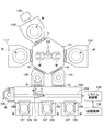
- FIG. 1 shows a processing system which is a semiconductor device manufacturing apparatus in the present embodiment.
- This processing system has four processing apparatuses 111, 112, 113, 114, a substantially hexagonal common transfer chamber 121, a first load lock chamber 122 and a second load lock chamber 123 having a load lock function, and an elongated introduction.
- a gate valve G is provided between each of the four processing devices 111 to 114 and the substantially hexagonal common transfer chamber 121.
- Gate valves G are also provided between the common transfer chamber 121 and the first load lock chamber 122 and the second load lock chamber 123, respectively. Gate valves G are also provided between the first load lock chamber 122 and the second load lock chamber 123 and the introduction-side transfer chamber 124. Each gate valve G can be opened and closed. When the gate valve G is opened, the wafer W can be moved between apparatuses. For example, three introduction ports 125 are connected to the introduction-side transfer chamber 124 via an opening / closing door 126, and a cassette container 127 in which a plurality of wafers W are stored is accommodated in the introduction port 125. In addition, an orienter 128 is provided in the introduction-side transfer chamber 124, and the wafer W is positioned.
- a transfer mechanism 131 having a pickup that can bend and stretch in order to transfer the wafer W is provided in the transfer chamber 121.
- the introduction-side transfer chamber 124 is provided with an introduction-side transfer mechanism 132 having a pickup that can bend and stretch to transfer the wafer W.
- the introduction-side transport mechanism 132 is supported in a slidable state on a guide rail 133 provided in the introduction-side transport chamber 124.
- the wafer W is, for example, a silicon wafer or the like, and is stored in the cassette container 127.
- the wafer W is transferred from the introduction port 125 to the first load lock chamber 122 or the second load lock chamber 123 by the introduction side transfer mechanism 132.
- the wafer W transferred to the first load lock chamber 122 or the second load lock chamber 123 is transferred to the four processing apparatuses 111 to 114 by the transfer mechanism 131 provided in the common transfer chamber 121.
- the wafer W is also transferred by the transfer mechanism 131 when the wafer W is moved between the four processing apparatuses 111 to 114. By moving between the processing apparatuses 111 to 114 in this way, the processing on the wafer W is performed in each of the processing apparatuses 111 to 114.
- Such control of the transfer and processing of the wafer W is performed by the system control unit 134 (control unit), and a program or the like for performing system control is stored in the storage medium 136.
- the system control unit 134 is an arbitrary combination of hardware and software, mainly a CPU of a computer, a memory, a program loaded in the memory, a storage unit such as a hard disk for storing the program, and a network connection interface. It is realized by. It will be understood by those skilled in the art that there are various modifications to the implementation method and apparatus.
- the first processing apparatus 111 is for forming a MnOx film, and has a gas supply system for supplying a film forming source gas to the processing space.
- the second processing apparatus 112 is for performing a hydrogen radical process, an inert gas annealing process, or a reducing atmosphere annealing process, and includes a gas supply system that supplies necessary gas to the processing space.
- the third processing apparatus 113 is for forming a Ru film, and includes a gas supply system that supplies a film forming source gas to the processing space.
- the fourth processing apparatus 114 is for forming a metal film such as a Cu film, and includes a gas supply system that supplies a film forming source gas to the processing space.
- a remote plasma generator 120 for generating atomic hydrogen is connected to the second processing apparatus 112, and atomic hydrogen generated by passing hydrogen through the remote plasma generator 120 is transferred to the wafer W.
- Irradiation can perform hydrogen radical treatment.
- a plasma generation unit may be provided inside the second processing apparatus 112, or a heating filament is provided for heating.
- the structure of generating atomic hydrogen may be used.
- a reducing atmosphere annealing process is performed by supplying hydrogen into the chamber of the second processing apparatus 112 and heating it.
- the wafer W may be pre-processed (for example, degas) in the first processing apparatus 111 or the like.
- the oxidizing atmosphere annealing process can be performed by the third processing apparatus 113, for example.
- the processing performed in the first processing device 111, the second processing device 112, and the third processing device 113 can be performed by one processing device 116.
- the processing apparatus 116 to which the remote plasma generation unit 120 is connected is connected to the common transfer chamber 121 via the gate valve G.
- a processing apparatus 117 for performing pretreatment (for example, degassing) of the wafer W may be provided as shown in FIG.
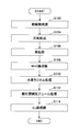
- the method for manufacturing a semiconductor device in the present embodiment is a method for manufacturing a semiconductor device having a multilayer wiring structure, and forms a wiring between layers. Is omitted.
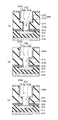
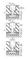
- an insulating film to be an interlayer insulating film is formed (insulating film forming step). Specifically, first, as shown in FIG. 4A, a first conductive film (wiring layer) 212 made of copper or the like is formed on the surface of an insulating film 211 formed on a substrate 210 such as a silicon substrate. Prepare the configuration. This configuration can be formed by a procedure similar to that of a second conductive film (Cu film) 230 (and Mn silicate film 222b and the like) described later.
- a diffusion prevention film 213 such as SiCN and an insulating film 214 made of SiO 2 or the like serving as an interlayer insulating film are stacked on this structure (insulating film forming step).
- the insulating film 211 and the insulating film 214 can be formed using TEOS containing silicon oxide or Low-k.
- the first conductive film 212 is connected to a transistor (not shown) formed on the surface of the substrate 210 and other wiring.
- the diffusion prevention film 213 may contain not only the above-described SiCN but also SiC or SiN as a main component.
- the insulating film 211 and the insulating film 214 are not limited to the above-described TEOS, but may be composed mainly of SiOC or SiOCH as Low-k.
- a Cu diffusion barrier film is formed between the insulating film 211 and the first conductive film 212, but the description is omitted here.
- a recess 215 (opening) is formed in the insulating film 214 and the diffusion prevention film 213 (recess formation step). Specifically, as shown in FIG. 4C, predetermined regions of the insulating film 214 and the diffusion prevention film 213 are removed by etching or the like until the surface of the first conductive film 212 is exposed, thereby forming a recess 215. .
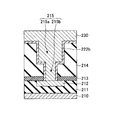
- the recess 215 includes an elongated groove (trench) 215a and a via hole 215b formed in a part of the bottom of the groove 215a. The first bottom 215c of the via hole 215b The conductive film 212 is exposed.
- Such a recess 215 is formed by, for example, applying a photoresist to the surface of the insulating film 214, exposing the exposure device by exposure, RIE (Reactive). It can be formed by repeating an etching process such as Ion Etching.
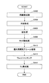
- step 106 degas processing, cleaning processing, or the like is performed as preprocessing. Thereby, the inside of the recess 215 is cleaned.
- cleaning treatment include H 2 annealing treatment, H 2 plasma treatment, Ar plasma treatment, and dry cleaning treatment using an organic acid.
- the degas treatment by heating is performed in an inert gas atmosphere such as N 2 , Ar, and He under the conditions of wafer temperature: 250 to 400 ° C., pressure: 13 to 2670 Pa, treatment time: 30 to 300 seconds,
- the wafer temperature is 300 ° C.
- the pressure is 1330 Pa
- the processing time is 120 seconds.
- the removal of natural copper oxide by H 2 annealing treatment may be performed in an H 2 atmosphere (in this case, an inert gas such as N 2 , Ar, or He may be added.
- the H 2 concentration is 1 to 100 vol%).
- processing time 30 to 300 seconds, preferably, for example, forming gas (3% H 2 + 97% Ar) atmosphere, wafer temperature : 300 ° C., pressure: 1330 Pa, treatment time: 120 seconds.
- the metal oxide film can be a film containing Mn such as a MnOx film.
- the metal oxide film can be formed by an ALD method. Specifically, as shown in FIG. 5A, the substrate 210 is heated to 100 to 250 ° C., for example, 130 ° C., and an Mn precursor such as (EtCp) 2 Mn and H 2 O are alternately supplied. As a result, the MnOx film 220 is formed. Thereby, the MnOx film 220 is formed on the bottom 215c of the via hole 215b, the side surface 215d of the recess 215, and the like.
- the MnOx film 220 that is formed on the bottom 215c of the via hole 215b is referred to as the MnOx film 221 and the MnOx film 222 that is formed on the side surface 215d of the recess 215 is described.
- the MnOx film 220 is also formed on the upper surface of the insulating film 214, the MnOx film 220 formed in this manner is assumed to change in the same manner as the MnOx film 222.
- the MnOx film may be formed not only by the above-described ALD method but also by a thermal CVD method or a plasma CVD method.
- the substrate 210 is heated to 150 to 400 ° C., for example, 200 ° C., and a Mn precursor of (EtCp) 2 is supplied to form a MnOx film.
- a MnOx film is formed on the side surface 215d of the recess 215 and the like.
- the natural oxide film (CuOx) on the Cu surface cannot be completely removed, a MnOx film is formed on the bottom surface of the recess where Cu is exposed by the reaction between the Mn precursor and the CuOx. .
- a cyclopentadienyl manganese compound such as bis (alkylcyclopentadienyl) manganese represented by the general formula Mn (RC 5 H 4 ) 2 .
- Carbonyl manganese compounds such as decacarbonyl 2 manganese (Mn 2 (CO) 10 ) and methylcyclopentadienyl tricarbonyl manganese ((CH 3 C 5 H 4 ) Mn (CO) 3 ).
- a beta diketone manganese compound such as bis (dipivaloylmethanato) manganese (Mn (C 11 H 19 O 2 ) 2 ).
- Amidinates such as bis (N, N′-dialkylacetamidinate) manganese represented by the general formula Mn (R 1 N—CR 3 —NR 2 ) 2 disclosed in US Publication No. US2009 / 0263965A1 Manganese compounds.
- R, R 1 , R 2 and R 3 are alkyl groups described by —C n H 2n + 1 (n is an integer of 0 or more), and Z is —C n H 2n — (n is 0 And an alkylene group described by the above integer).
- (EtCp) 2 Mn [ Mn (C 2 H 5 C 5 H 4 ) 2 ] because it is liquid at room temperature, has a sufficient vapor pressure for bubbling supply, and has high thermal stability. Is preferably used.
- reaction gas other than H 2 O examples include oxygen-containing gases, such as N 2 O, NO 2 , NO, O 2 , O 3 , H 2 O 2 , CO, CO 2 , alcohol, Aldehydes, carboxylic acids, carboxylic anhydrides, esters, organic acid ammonium salts, organic acid amine salts, organic acid amides, and organic acid hydrazides can be used. Moreover, you may use combining these some oxygen containing gas. Note that liquids at room temperature are supplied into the processing chamber in a gas or vapor state by heating and vaporizing.
- this oxide film may be formed of other metal oxides, and more preferably Mg, Al, Ca, One or more elements selected from Ti, V, Cr, Mn, Fe, Co, Ni, Ge, Sr, Y, Zr, Nb, Mo, Rh, Pd, Sn, Ba, Hf, Ta and Ir You may form by what contains these oxides. Among these, it can form silicate, can be dissolved in Cu, has a large diffusion coefficient for Cu (high diffusion rate in Cu), and dissolves in acids that have no oxidizing power (weak). Mn is the most preferable from the viewpoint of being able to.
- step 110 hydrogen radical treatment is performed (hydrogen radical treatment step). Specifically, atomic hydrogen is generated by remote plasma, plasma, a heating filament, or the like, and the generated atomic hydrogen is irradiated on the surface of the MnOx film 220.
- atomic hydrogen is generated by the remote plasma generated in the remote plasma generation unit 120 shown in FIGS. 1 and 2, and the MnOx 220 is formed on the substrate 210 using the generated atomic hydrogen. Irradiate the surface.
- heat treatment is preferably performed together.
- the substrate 210 is heated to 300 ° C.
- the hydrogen radical treatment is performed in a gas atmosphere of H 2 : 10% and Ar: 90% at a treatment pressure of 40 Pa, an input power of 2.5 kW, and a substrate heating temperature of 300 ° C. For seconds.
- the MnOx film 222 formed on the side surface 215d of the recess 215 in the MnOx film 220 is reduced to become the Mn film 222a.
- the MnOx film 221 formed on the bottom 215c of the via hole 215b is reduced, and the reduced Mn diffuses into the first conductive film 212 made of copper or the like, so that the MnOx film 221 disappears. Therefore, the first conductive film 212 made of copper or the like is exposed at the bottom 215c of the via hole 215b.
- the heating temperature of the substrate 210 is preferably room temperature to 450 ° C., more preferably 200 ° C. to 400 ° C., and further preferably about 300 ° C.
- the H 2 concentration in Ar is preferably 1 to 20%, more preferably 3 to 15%, and further preferably H 2 : 10% and Ar: 90%.
- the processing pressure is preferably 10 to 500 Pa, more preferably 20 to 100 Pa, and further preferably 40 Pa.
- the input power is preferably 1 to 5 kW, more preferably 1.5 to 3 kW, and further preferably 2.5 kW.
- the treatment time is preferably 5 to 300 seconds, more preferably 10 to 100 seconds, and further preferably 60 seconds.
- a degas step may be performed between the MnOx film 220 in step 108 and the hydrogen radical treatment in step 110.
- annealing is performed in an oxidizing atmosphere (annealing process).
- the substrate heating temperature is 200 to 500 ° C., more preferably 250 to 350, for 30 to 1800 seconds under conditions of a processing pressure of 13 to 2670 Pa.
- Annealing is performed at a temperature of ° C.
- the oxygen-containing gas other than O 2 for example, H 2 O, N 2 O, NO 2 , NO, O 3 , H 2 O 2 , CO, and CO 2 can be used.
- an oxygen-containing gas such as H 2 O
- the oxygen-containing gas is externally contained.
- annealing may be performed while supplying an inert gas.
- the oxygen-containing gas can be supplied from the gas supply system of the processing apparatus to the wafer processing space, and components contained in the substrate can be degassed and used as the oxygen-containing gas.
- the MnOx film 222 formed on the side surface 215d and the like of the recess 215 in the MnOx film 220 by the hydrogen radical treatment in step 110 is all reduced to become the Mn film 222a.
- the MnOx film 222 may not be reduced to become the Mn film 222a.
- MnOx film 222 only the upper layer side of the MnOx film 222 that is exposed and not in contact with the insulating film 214 is reduced by the hydrogen radical treatment to become the Mn film (222a), while the lower layer in contact with the insulating film 214 It is conceivable that the side does not receive the reducing action of hydrogen radicals, and reacts with silicon oxide in the insulating film 214 by heat during the hydrogen radical treatment to form a Mn silicate (MnSixOy) film (222b). In such a case, the formation of the Mn silicate has already been completed, and as a final structure, the Mn silicate film 222b is formed between the insulating film 214 and the second conductive film 230. Therefore, it is possible to omit the oxidizing atmosphere annealing process in step 112 (S112).
- the reduced Mn film 222a formed on the side surface 215d and the like of the recess 215 becomes the silicon oxide in the insulating film 214 forming the side surface 215d and the like of the recess 215.
- Mn silicate (MnSixOy) film 222b To form a Mn silicate (MnSixOy) film 222b.
- the reaction in which the Mn film 222a is silicated to become the Mn silicate film 222b will be described in more detail based on the following. Specifically, by annealing the wafer W in an oxidizing atmosphere, the Mn film 222a reacts with the SiO 2 component contained in the base to be silicated, and the chemical reaction formula is referred to for the mechanism that becomes the Mn silicate layer 222b. While explaining.
- a chemical reaction formula between metal manganese (Mn) and silicon dioxide (SiO 2 ) is shown below.
- Each chemical reaction formula shows an equilibrium state at 300K.
- the amount of heat on the right side is the amount of heat (kJ) per mol of manganese (Mn), and represents the amount of Gibbs free energy change (hereinafter referred to as Gr change amount ( ⁇ Gr)).
- Gr change amount ⁇ Gr
- Gibbs' free energy tries to decrease spontaneously. Therefore, it is known that a chemical reaction in which the Gr change amount is negative occurs spontaneously, and a chemical reaction in which the Gr change amount is positive does not occur spontaneously.
- thermodynamic calculation a commercially available thermodynamic database was used.
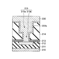
- the second conductive film 230 is formed (second conductive film forming step).
- the second conductive film is typically a metal film such as Cu.
- the second conductive film 230 such as Cu is formed by any one of CVD method, ALD method, PVD method, electrolytic plating method, electroless plating method, and supercritical CO 2 method. Form.
- the method for forming the second conductive film 230 may be a combination of the above methods.
- Cu is deposited by electrolytic plating to form second conductive film 230 by Cu.
- planarization is performed by CMP (Chemical Mechanical Polishing) or the like as necessary to remove the second conductive film 230 and the Mn silicate film 222b exposed from the recess 215.
- CMP Chemical Mechanical Polishing
- the formation of the MnOx film 220 in Step 108, the hydrogen radical treatment in Step 110, and the oxidizing atmosphere annealing treatment in Step 112 may be performed in the same chamber (processing apparatus), or different chambers ( Processing apparatus). From the viewpoint of safety, it is preferable that the hydrogen radical process in step 110 and the oxidizing atmosphere annealing process in step 112 are performed in different chambers (processing apparatuses). In the case where the hydrogen radical treatment in step 110 and the oxidizing atmosphere annealing treatment in step 112 are performed in the same chamber (processing apparatus), H is considered in consideration of reactivity with hydrogen as an oxygen-containing gas used in the oxidizing atmosphere annealing treatment. It is preferable to use 2 O or CO 2 . As a method for supplying the oxygen-containing gas, the oxygen-containing gas can be supplied from the gas supply system of the processing apparatus to the wafer processing space, and components contained in the substrate can be degassed and used as the oxygen-containing gas.
- the manufacturing method in the present embodiment since Mn silicate film 222b is formed between insulating film 214 and second conductive film 230, Cu or the like contained in second conductive film 230 is contained in insulating film 214. And O 2 or H 2 O contained in the insulating film 214 can be prevented from diffusing into the second conductive film 230.
- the second conductive film 230 is in direct contact with copper or the like forming the first conductive film 212, sufficient conduction can be obtained and occurrence of poor conduction can be suppressed.
- the Cu multilayer wiring can be miniaturized, and a high-speed and reliable electronic device can be obtained though it is small by increasing the speed and miniaturization of the semiconductor device (device).
- the method for manufacturing a semiconductor device in the present embodiment is a method for manufacturing a semiconductor device having a multilayer wiring structure, and forms a wiring between layers. Is omitted.
- the semiconductor device manufacturing apparatus of the first embodiment can be used.
- MnSiO 3 is formed by reducing atmosphere annealing using a reducing gas (where R 1 to R 7 are hydrogen (H) or hydrocarbon) or inert gas annealing using an inert gas. Different from the first embodiment.
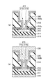
- Steps 202 to 208 the configuration shown in FIG. 9A is prepared by the same processing procedure (Steps 202 to 208) as Steps 102 to 108 (FIG. 3) in the first embodiment.
- Various materials can be the same as those described in the first embodiment.
- step 210 an annealing process using an inert gas or a reducing gas is performed (annealing process).
- hydrogen, CO, amine, or the like NR 1
- an inert gas such as helium (He), argon (Ar), neon (Ne), or nitrogen (N 2 ).
- R 2 R 3 ), hydrazine or an analog thereof N 2 R 4 R 5 R 6 R 7 ) or the like is performed in a reducing atmosphere annealing process in an atmosphere to which a reducing gas is added.
- R 1 to R 7 are hydrogen (H) or hydrocarbon.
- Examples of the analog of amine (NH 3 ) include methylamine (CH 3 NH 2 ), ethylamine (C 2 H 5 NH 2 ), dimethylamine ((CH 3 ) 2 NH), and trimethylamine ((CH 3 ) 3 N) and the like.
- Examples of analogs of hydrazine (N 2 H 4 ) include methyl hydrazine (CH 3 NNH 3 ), dimethyl hydrazine ((CH 3 ) 2 NNH 2 ), and trimethylhydrazine ((CH 3 ) 3 NNH). .
- a substrate heating temperature of 200 to 450 ° C. is more preferable for 30 to 1800 seconds in a gas atmosphere of H 2 : 3% and Ar: 97% under a processing pressure of 13 to 2670 Pa. Is annealed to 250 to 350 ° C.
- the reducing atmosphere annealing treatment step is described, but the inert gas annealing treatment step may be performed instead of this reducing atmosphere annealing treatment step only when MnOx is made of only MnO. Good.
- the MnOx film 222 formed on the side surface 215d and the like of the recess 215 reacts with the silicon oxide in the insulating film 214 forming the side surface 215d and the like of the recess 215. Then, a Mn silicate (MnSixOy) film 222b is formed. Note that since the MnOx film 221 formed on the bottom 215c of the via hole 215b is formed on the first conductive film 212 such as Cu, the MnOx film 221 is not changed into a silicate and is not changed. Absent. The MnOx film 222 formed on the diffusion prevention film 213 is hardly silicated and remains MnOx. However, the diffusion prevention film 213 is made of SiCN or the like and has a diffusion prevention function. It doesn't matter if it isn't.
- the reaction in which the MnOx film 222 is silicated to become the Mn silicate film 222b will be described in more detail based on the following. Specifically, the mechanism in which the MnOx film 222 reacts with the SiO 2 component contained in the base to be silicate by annealing in a reducing atmosphere to form the Mn silicate layer 222b will be described with reference to a chemical reaction formula. To do.
- a chemical reaction formula between manganese oxide (MnO and Mn 2 O 3 ) and silicon dioxide (SiO 2 ) is shown below.
- Each chemical reaction formula shows an equilibrium state at 300K.
- the amount of heat on the right side is the amount of heat (kJ) per mol of manganese (Mn), and the amount of Gibbs free energy change (hereinafter referred to as Gr change amount ( ⁇ Gr)) is represented by two significant digits.
- Gr change amount ⁇ Gr
- Gibbs' free energy tries to decrease spontaneously. Therefore, it is known that a chemical reaction in which the Gr change amount is negative occurs spontaneously, and a chemical reaction in which the Gr change amount is positive does not occur spontaneously.
- thermodynamic calculation a commercially available thermodynamic database was used.
- Mn 2 O 3 can be converted to MnO by introducing hydrogen from the chemical reaction formula shown in (7) above. Further, from the chemical reaction formula shown in (1) above, MnO can be silicated to become Mn silicate (MnSixOy). Therefore, by introducing hydrogen, Mn 2 O 3 is silicated to form Mn. It can be silicate (MnSixOy).
- MnO can be silicated by annealing.
- B2 Mn 2 O 3 + 2SiO 2 + 0.5NH 3 ⁇ 2MnSiO 3 + 0.25N 2 O + 0.75H 2 O-12 ( ⁇ Gr (kJ / Mn-mol))
- B3 Mn 2 O 3 + SiO 2 + 0.5NH 3 ⁇ Mn 2 SiO 4 + 0.25N 2 O + 0.75H 2 O-16 ( ⁇ Gr (kJ / Mn-mol))
- N 2 H 4 is introduced as a reducing gas are shown.
- step 212 hydrogen radical treatment is performed (hydrogen radical treatment step). Since the procedure of the hydrogen radical treatment is the same as that in the first embodiment, detailed description thereof is omitted.
- the MnOx film 221 formed on the bottom 215c of the via hole 215b is reduced, and the reduced Mn diffuses into the first conductive film 212 made of copper or the like. Therefore, the MnOx film 221 disappears. Therefore, the first conductive film 212 made of copper or the like is exposed at the bottom 215c of the via hole 215b.
- the Mn silicate film 222b formed on the side surface 215d of the recess 215 is considered to be hardly changed because it is relatively stable as a substance.
- step 214 As shown in FIG. 10, a second conductive film 230 such as Cu is formed (second conductive film forming step). Since the procedure for forming the second conductive film is the same as that in the first embodiment, detailed description thereof is omitted.
- planarization is performed by CMP or the like as necessary, and the second conductive film 230 and the Mn silicate film 222b exposed from the recess 215 are removed.
- the formation of the MnOx film 220 in Step 208, the inert gas annealing process or the reducing atmosphere annealing process in Step 210, and the hydrogen radical process in Step 212 may be performed in the same chamber (processing apparatus). Moreover, you may carry out by each different chamber (processing apparatus). In step 208, the film formation process in step 208 and the annealing process step in step 210 can be performed simultaneously by forming a film in a state where hydrogen is mixed.
- the manufacturing method in the present embodiment since Mn silicate film 222b is formed between insulating film 214 and second conductive film 230, Cu or the like contained in second conductive film 230 is contained in insulating film 214. And O 2 or H 2 O contained in the insulating film 214 can be prevented from diffusing into the second conductive film 230.
- the second conductive film 230 is in direct contact with copper or the like forming the first conductive film 212, sufficient conduction can be obtained and occurrence of poor conduction can be suppressed.
- the Cu multilayer wiring can be miniaturized, and a high-speed and reliable electronic device can be obtained though it is small by increasing the speed and miniaturization of the semiconductor device (device).
- the contents other than the above are the same as in the first embodiment.
- a third conductive film that functions as an adhesion layer for improving the adhesion between the Mn silicate (MnSixOy) film 222b and the second conductive film 230 is formed.
- the lattice constant of Ru (002) is 2.14 angstroms
- the lattice constant of Cu (111) is 2.09 angstroms. Since Ru has a close lattice constant with Cu and good wettability with each other, high adhesion and good embedding of the second conductive film 230 such as Cu into the recess 215 can be expected.
- the method for manufacturing a semiconductor device in the present embodiment is a method for manufacturing a semiconductor device having a multilayer wiring structure, and forms a wiring between layers. Is omitted.
- the semiconductor device manufacturing apparatus of the first embodiment can be used.
- the configuration shown in FIG. 13B is prepared by processing procedures (steps 302 to 310) similar to steps 102 to 110 (FIG. 3) in the first embodiment.
- steps 302 to 310 similar to steps 102 to 110 (FIG. 3) in the first embodiment.
- Various materials can be the same as those described in the first embodiment.
- the third conductive film (Ru film) 240 is formed (third conductive film forming step). Specifically, as shown in FIG. 13C, the substrate 210 is heated to about 200 ° C. using an organometallic raw material containing Ru (eg, Ru carbonyl), and the third conductive film 240 is formed by CVD. Film.
- the third conductive film 240 is a metal material and is formed on the inner surface of the recess 215 including the bottom surface 215c of the via hole 215b. That is, the third conductive film 240 is formed on the surfaces of the first conductive film 212 and the Mn film 222a exposed in the recess 215. On the bottom surface 215c of the via hole 215b, the Mn film 222a is not formed on the exposed surface of the first conductive film 212 as described above. A third conductive film 240 is formed.
- annealing is performed in an oxidizing atmosphere (annealing process).
- the substrate heating temperature is 200 to 500 ° C., more preferably 250 to 350, for 30 to 1800 seconds under conditions of a processing pressure of 13 to 2670 Pa.
- Annealing is performed at a temperature of ° C.
- the oxygen-containing gas other than O 2 for example, H 2 O, N 2 O, NO 2 , NO, O 3 , H 2 O 2 , CO, and CO 2 can be used.
- an oxygen-containing gas such as H 2 O
- the oxygen-containing gas is externally contained.
- annealing may be performed while supplying an inert gas.
- the oxygen-containing gas can be supplied from the gas supply system of the processing apparatus to the wafer processing space, and components contained in the substrate can be degassed and used as the oxygen-containing gas.
- the reduced Mn film 222a formed on the side surface 215d and the like of the concave portion 215 becomes the silicon oxide in the insulating film 214 forming the side surface 215d and the like of the concave portion 215.
- Mn silicate (MnSixOy) film 222b To form a Mn silicate (MnSixOy) film 222b.
- a predetermined degree of vacuum or a predetermined oxygen partial pressure be maintained between the hydrogen radical treatment in step 310 and the formation of the third conductive film 240 in step 312.
- the pressure is maintained at 1 ⁇ 10 ⁇ 4 Pa or less. Therefore, the hydrogen radical treatment in step 310 and the formation of the third conductive film 240 in step 312 are performed in the same chamber as shown in FIG. 2, or the hydrogen radical treatment as shown in FIG.
- the chamber for performing radical treatment and the chamber for forming the third conductive film 240 are connected by a common transfer chamber 121 capable of maintaining a predetermined degree of vacuum, and the wafer W is moved through the common transfer chamber 121. It is preferable that it can be made.
- a cooling process may be provided between the hydrogen radical treatment in step 310 and the formation of the third conductive film 240 in step 312 to cool the substrate 210 to the Ru film formation temperature or lower, for example, room temperature.
- the film thickness of the third conductive film 240 to be formed is 0.5 to 5 nm, and the film formation of the third conductive film 240 may be performed by the ALD method in addition to the CVD method.
- metal materials other than Ru for example, Fe, Co, Ni, Rh, Pd, Os, Ir, and Pt It may contain 1 or 2 or more elements chosen from these. Furthermore, it may contain one or more elements selected from platinum group elements. These are excellent in adhesiveness with Cu and have the same function as the seed Cu layer because they conduct electricity.
- step 316 As shown in FIG. 14B, a second conductive film 230 such as Cu is formed (second conductive film forming step). Since the procedure for forming the second conductive film is the same as that in the first embodiment, detailed description thereof is omitted.
- planarization is performed by CMP or the like as necessary, and the second conductive film 230 and the Mn silicate film 222b exposed from the recess 215 are removed.
- the formation of the MnOx film 220 in Step 308 and the hydrogen radical treatment in Step 310 may be performed in the same chamber (processing apparatus) or in different chambers (processing apparatuses). .
- the third conductive film 240 and the Mn silicate film 222b are formed between the insulating film 214 and the second conductive film 230, Cu contained in the second conductive film 230 is formed. And the like can be prevented from diffusing into the insulating film 214, and O 2 and H 2 O contained in the insulating film 214 can be prevented from diffusing into the second conductive film 230.
- the second conductive film 230 is in contact with the first conductive film 212 through the third conductive film 240, which is a highly conductive metal material, sufficient conduction can be obtained and the occurrence of poor conduction. Can be suppressed.
- the wettability with the second conductive film 230 (Cu) is improved by interposing the third conductive film 240, the adhesion is improved and the embedding property of the second conductive film 230 (Cu) is improved. It can be expected to improve.
- the Cu multilayer wiring can be miniaturized, and a high-speed and reliable electronic device can be obtained though it is small by increasing the speed and miniaturization of the semiconductor device (device).
- the step of forming the third conductive film 240 in Step 312 is replaced with the hydrogen radical in Step 212. What is necessary is just to insert between a processing process and the film-forming process of Cu film
- This embodiment is different from the second embodiment in that the MnOx film 221 formed on the bottom of the recess 215 is selectively removed by wet etching.
- the method for manufacturing a semiconductor device in the present embodiment is a method for manufacturing a semiconductor device having a multilayer wiring structure, and forms a wiring between layers. Is omitted. In this embodiment, a part of the semiconductor device manufacturing apparatus in the first embodiment can be used.
- the configuration shown in FIG. 17A is prepared by the same processing procedure (steps 402 to 408) as steps 102 to 108 (FIG. 3) in the first embodiment.
- steps 402 to 408 steps 102 to 108
- Various materials can be the same as those described in the first embodiment.
- step 410 an inert gas, a hydrogen-containing gas, or a reducing atmosphere annealing process is performed (inert gas annealing process or reducing atmosphere annealing process). Since this procedure is the same as that of the second embodiment (step 210 (S210)), detailed description thereof is omitted.
- the MnOx film 222 formed on the side surface 215d and the like of the recess 215 reacts with the silicon oxide in the insulating film 214 forming the side surface 215d and the like of the recess 215.
- a Mn silicate (MnSixOy) film 222b is formed. Since the MnOx film 221 formed on the bottom 215c of the via hole 215b is formed on the first conductive film 212 such as Cu, it is not silicated and changes as it is in the MnOx film 221. There is no.
- the MnOx film 222 formed on the diffusion prevention film 213 is hardly silicated and remains MnOx.
- the diffusion prevention film 213 is made of SiCN or the like and has a diffusion prevention function. It doesn't matter if it isn't.
- step 412 wet etching using hydrochloric acid is performed. Specifically, by immersing an inert gas annealing process or a reducing atmosphere annealing process in hydrochloric acid or the like, the first conductive film 212 such as Cu is formed on the first conductive film 212 as shown in FIG. The formed MnOx film 221 is removed by dissolving with hydrochloric acid. At this time, since the Mn silicate film 222b formed on the side surface 215d of the recess 215 is silicated, it is not attacked by hydrochloric acid and is not removed.
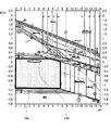
- FIG. 19 shows the relationship between the pH value and the potential of the standard hydrogen electrode.
- a range 19A in which Mn is dissolved but Cu is not dissolved Mn is ionized but Cu is not ionized (a range of about ⁇ 1.2 V to 0.1 V in the figure)).
- Mn is ionized but Cu is not ionized
- a range 19B in which Mn is dissolved but Cu and MnSiO 3 are not dissolved in the present embodiment, wet etching is performed under conditions in the range 19B (about ⁇ 0.1 V or more and 0.1 V or less). As a result, as shown in FIG.
- the recess 215 overlying the first conductive film 212 such as Cu without removing the Mn silicate film 222b formed on the side surface 215d of the recess 215 and the like.
- the MnOx film 221 formed on the bottom surface 215c can be removed.
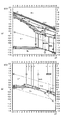
- FIG. 19 shows the relationship between the pH value in Mn shown in FIG. 20A and the potential of the standard hydrogen electrode, and the pH value in Cu shown in FIG. 20B and the potential of the standard hydrogen electrode. It is obtained by superimposing the above relationship.
- the horizontal axis indicates the pH value
- the vertical axis indicates the potential of the standard hydrogen electrode.
- hydrochloric acid was used was demonstrated in description in this Embodiment, you may use an acetic acid, a citric acid, etc.
- step 414 a second conductive film 230 such as Cu is formed (second conductive film formation step). Since the procedure for forming the second conductive film is the same as that in the first embodiment, detailed description thereof is omitted.
- planarization is performed by CMP or the like as necessary, and the second conductive film 230 and the Mn silicate film 222b exposed from the recess 215 are removed.
- the formation of the MnOx film 220 in step 408 and the inert gas annealing process or reducing atmosphere annealing process in step 410 may be performed in the same chamber (processing apparatus), or different chambers (processing apparatus). Apparatus).
- the film formation process in step 408 and the annealing process step in step 410 can be performed simultaneously by forming a film in a state where hydrogen is mixed.
- a cluster tool may be formed by connecting a chamber (processing apparatus) for performing wet etching to the common transfer chamber 121.
- Mn silicate film 222b is formed between insulating film 214 and second conductive film 230, Cu or the like contained in second conductive film 230 is contained in insulating film 214. And O 2 or H 2 O contained in the insulating film 214 can be prevented from diffusing into the second conductive film 230.
- the second conductive film 230 is in direct contact with copper or the like forming the first conductive film 212, sufficient conduction can be obtained and occurrence of poor conduction can be suppressed.
- the MnOx film 221 formed in advance on the bottom surface 215c of the recess 215 is removed by wet etching, and Mn does not diffuse in the first conductive film 212, so that the wiring resistance is further increased. Can be lowered.
- the Cu multilayer wiring can be miniaturized, and a high-speed and reliable electronic device can be obtained though it is small by increasing the speed and miniaturization of the semiconductor device (device).
- the contents other than those described above are the same as those in the first or second embodiment.
- the present invention is not limited to the formation of the MnOx film described above, but also when the metal Mn film is formed by a film forming means such as a thermal ALD method, a thermal CVD method, a plasma ALD method, or a plasma CVD method. May be applicable.
- a Mn film is formed by heating the substrate 210 to 200 to 400 ° C., for example, 300 ° C., and supplying a Mn precursor such as the above-mentioned amidoaminoalkane manganese compound.
- a Mn film is usually formed on the bottom 215c of the via hole 215b, the side surface 215d of the recess 215, and the like.
- the MnOx film is formed on the bottom surface of the recess where Cu is exposed due to the reaction between the formed metal Mn and the CuOx. May be formed.
- the MnOx deposited on Cu is reduced by hydrogen radical treatment that irradiates the substrate with atomic hydrogen, and is removed by diffusing into Cu (the first lower conductive film) and disappearing. Is possible.
- the Cu film (second conductive film) in step 114 (S114) is formed after the oxidizing atmosphere annealing process in step 112 (S112) in FIG. 3 is performed. Indicated.
- Mn is also formed by performing the oxidation atmosphere annealing process similar to step 112 (S112) after the Cu film (second conductive film) similar to that in step 114 (S114) is formed. It can be silicated to obtain MnSixOy. The same applies to other embodiments.
- the annealing treatment in the oxidizing atmosphere in Step 314 (S314) is performed.
- the Ru film (third conductive film) in Step 312 (S312) may be formed after the oxidation atmosphere annealing process in Step 314 (S314).
- the oxidizing atmosphere annealing process in step 314 (S314) may be performed after the Cu film (second conductive film) is formed in step 316 (S316).
- the processing of each embodiment may be appropriately combined.
- the Ru film (third conductive film) can be formed in step 312 (S312) of FIG. 11 described in the third embodiment.
- the film formation process of the Ru film (third conductive film 240) in step 312 is performed between the hydrogen radical treatment process in step 212 and the film formation process of the Cu film (second conductive film 230) in step 214. Insert it.
- the present invention also includes the following forms (Item 1) to (Item 27).
- (Item 1) An insulating film is formed on the surface of the substrate, and an oxide film forming step of forming an oxide film made of a metal oxide in an opening (concave portion) formed in the insulating film; A hydrogen radical treatment step of irradiating atomic hydrogen after the oxide film deposition step; After the oxide film forming step, an oxygen annealing treatment step of heating in a state where oxygen is supplied; After performing the hydrogen radical treatment step and the oxygen annealing treatment step, an electrode formation step of forming an electrode made of metal inside the opening,
- a method for manufacturing a semiconductor device comprising: (Item 2) An insulating film is formed on the substrate surface, and an oxide film forming step of forming an oxide film made of a metal oxide in the opening formed in the insulating film; A hydrogen radical treatment step of irradiating atomic hydrogen after the oxide film deposition step; An electrode forming step of forming an electrode made of metal in the opening after
- An insulating film is formed on the substrate surface, and an oxide film forming step of forming an oxide film made of a metal oxide in the opening formed in the insulating film; After the oxide film formation step, a hydrogen annealing treatment step of heating in a state of supplying hydrogen, A hydrogen radical treatment step of irradiating atomic hydrogen after the hydrogen annealing treatment step; After performing the hydrogen annealing treatment step and the hydrogen radical treatment step, an electrode formation step of forming an electrode made of a metal inside the opening;
- a method for manufacturing a semiconductor device comprising: (Item 5) 5.
- An insulating film is formed on the substrate surface, and an oxide film forming step of forming an oxide film made of a metal oxide in the opening formed in the insulating film; After the oxide film formation step, a hydrogen annealing treatment step of heating in a state of supplying hydrogen, After the hydrogen annealing treatment step, a wet etching step of removing the oxide film on the bottom surface of the opening by wet etching, After performing the wet etching step, an electrode forming step of forming an electrode made of metal inside the opening,
- a method for manufacturing a semiconductor device comprising: (Item 8) 8.
- Item 9 Item 8. The method for manufacturing a semiconductor device according to Item 7, wherein the wet etching is performed using a neutral or acidic chemical solution.
- Item 10 Item 10. The method for manufacturing a semiconductor device according to Item 9, wherein an oxidation-reduction potential of the chemical solution is 0.1 V or less.
- Item 11 Item 10. The method for manufacturing a semiconductor device according to Item 9, wherein an oxidation-reduction potential of the chemical solution is ⁇ 1.2 V or more and 0.1 V or less. (Item 12) 12.
- the oxide film includes Mg, Al, Ca, Ti, V, Cr, Mn, Fe, Co, Ni, Ge, Sr, Y, Zr, Nb, Mo, Rh, Pd, Sn, Ba, Hf, Ta, and Ir. 13.
- the method for manufacturing a semiconductor device according to any one of items 1 to 12, wherein the semiconductor device is formed of an oxide containing an oxide of one or more elements selected from the above. (Item 14) 14. The method of manufacturing a semiconductor device according to any one of items 1 to 13, wherein the oxide film includes an oxide of Mn.
- a metal film (conductive film) deposition step is performed, and after the metal film deposition step is performed, an electrode formation step Which performs Items 1 to 14, wherein the metal film is formed of one or more elements selected from Fe, Co, Ni, Ru, Rh, Pd, Os, Ir, and Pt.
- a method for manufacturing a semiconductor device according to any one of the above. (Item 16) 16. The semiconductor device according to any one of items 4, 7, and 15, wherein an inert gas treatment step of heating in a state where an inert gas is supplied is performed instead of the hydrogen annealing treatment step. Production method.
- a film containing Mn is formed, Item 17.
- (Item 18) 18.
- the electrode was formed by one or more methods selected from a thermal CVD method, a thermal ALD method, a plasma CVD method, a plasma ALD method, a PVD method, an electrolytic plating method, an electroless plating method, and a supercritical CO2 method. 19.
- the semiconductor device manufacturing apparatus according to Item 21, wherein the oxide film is formed by ALD.
- Item 23 Item 23.
- Item 24 Having one or more chambers, In any of the chambers, a metal film is formed by thermal CVD or plasma CVD, In any one of the chambers, a hydrogen radical treatment that irradiates atomic hydrogen is performed. In any of the chambers, an annealing process is performed by heating in a state where hydrogen, oxygen, or an inert gas is supplied, An apparatus for manufacturing a semiconductor device, wherein an electrode made of a metal is formed in any of the chambers. (Item 25) Item 25.
- the semiconductor device manufacturing apparatus wherein the metal film is a film containing Mn.
- Item 26 26.
- the semiconductor device according to item 21 or 25, wherein the hydrogen radical treatment and the annealing treatment for heating in a state where hydrogen, oxygen, or an inert gas is supplied are performed in the same chamber.
- Item 27 Item 21 or 26, wherein the oxide film formation, the hydrogen radical treatment, and the annealing treatment in which the hydrogen, oxygen, or inert gas is supplied are performed in the same chamber.
Landscapes
- Chemical & Material Sciences (AREA)
- Internal Circuitry In Semiconductor Integrated Circuit Devices (AREA)
- General Chemical & Material Sciences (AREA)
- Chemical Kinetics & Catalysis (AREA)
- Engineering & Computer Science (AREA)
- Materials Engineering (AREA)
- Mechanical Engineering (AREA)
- Metallurgy (AREA)
- Organic Chemistry (AREA)
- Inorganic Chemistry (AREA)
- Chemical Vapour Deposition (AREA)
Abstract
Description
Chemical Vapor Deposition)法やプラズマCVD(Plasma Enhanced Chemical Vapor Deposition)法によりMn膜を成膜する場合においても、Cu表面の自然酸化膜(CuOx)が除去しきれずに残っている場合には、形成された金属Mnと前記CuOxとの反応により、Cuが露出している凹部の底面にもMnOx膜が形成される。このように形成されたMnOx膜は、Cuなどの金属に比べて高抵抗であるため、MnOx膜の上にCuからなる埋め込み電極を形成しても、MnOx膜を介しては十分な導通を得ることができず、導通不良となってしまうという問題点があった。
Mnの場合は、O2アニールによりMnSiO3が形成される。
MnOの場合は、不活性ガスアニールによりMnSiO3が形成される。
Mn3O4、Mn2O3、MnO2の場合は、水素、CO、アミン又はその類似物(NR1R2R3)、ヒドラジン又はその類似物(N2R4R5R6R7)等の還元ガス(ここで、R1~R7は、水素(H)又は炭化水素である。)を用いた還元雰囲気アニールによりMnSiO3が形成される。
という知見に基づくものである。
(半導体装置の製造装置)
本実施の形態における半導体装置の製造装置について説明する。尚、ウエハWとは、基板または膜が成膜された基板を意味する。図1は、本実施の形態における半導体装置の製造装置である処理システムを示す。この処理システムは、4つの処理装置111、112、113、114と、略六角形状の共通搬送室121と、ロードロック機能を有する第1ロードロック室122及び第2ロードロック室123と、細長い導入側搬送室124とを有する。4つの処理装置111~114と略六角形状の共通搬送室121との間には各々ゲートバルブGが設けられている。共通搬送室121と第1ロードロック室122及び第2ロードロック室123との間にも各々ゲートバルブGが設けられている。第1ロードロック室122及び第2ロードロック室123と導入側搬送室124との間にも各々ゲートバルブGが設けられている。各々のゲートバルブGは開閉可能であり、ゲートバルブGが開くことにより装置間等においてウエハWを移動させることができる。導入側搬送室124には、例えば、3つの導入ポート125が開閉ドア126を介し接続されており、導入ポート125には複数のウエハWが収納されたカセット容器127が納められている。また、導入側搬送室124には、オリエンタ128が設けられており、ウエハWの位置決め等がなされる。
次に、図3及び図4~図6に基づき本実施の形態における半導体装置の製造方法について説明する。本実施の形態における半導体装置の製造方法は、多層配線構造を有する半導体装置の製造方法であって、層間における配線を形成するものであるため、形成されている半導体素子及び半導体素子の形成方法については省略されている。
Ion Etching)等によるエッチングの工程を繰り返すことにより形成することができる。
・一般式Mn(RC5H4)2で表されるビス(アルキルシクロペンタジエニル)マンガンのようなシクロペンタジエニル系マンガン化合物。
・デカカルボニル2マンガン(Mn2(CO)10)やメチルシクロペンタジエニルトリカルボニルマンガン((CH3C5H4)Mn(CO)3)のようなカルボニル系マンガン化合物。
・ビス(ジピバロイルメタナト)マンガン(Mn(C11H19O2)2)のようなベータジケトン系マンガン化合物。
・米国公報 US2009/0263965A1号に開示されている一般式Mn(R1N-CR3-NR2)2で表されるビス(N,N'-ジアルキルアセトアミジネート)マンガンのようなアミジネート系マンガン化合物。
・国際公開第2012/060428号に開示されている一般式Mn(R1N-Z-NR2 2)2で表されるビス(N,N'-1-アルキルアミド-2-ジアルキルアミノアルカン)マンガンのようなアミドアミノアルカン系マンガン化合物。
上記の(A)に示される化学反応式では、左辺と右辺の酸素量が釣り合っておらず反応式として成り立たない。よって、左辺から右辺への反応が進み得ないこと、つまり、シリケート化される可能性が無いことがわかる。このことから、Mnについては、単なる熱処理だけではシリケート化が起こらないため、Mnとして残存する。
上記の(B)に示される化学反応式より、Mnの場合、酸素が供給されることで左辺から右辺への反応が進み得ること、つまり、シリケート化される可能性がある。このことから、酸素の導入により、Mnがシリケート化されて、MnSixOyとなり得る。尚、上記のシリケート化反応は、O2以外に、H2OやCO2でも反応が進み得ることを熱力学計算で確認している。
次に、図7及び図8~図10に基づき第2の実施の形態について説明する。本実施の形態における半導体装置の製造方法は、多層配線構造を有する半導体装置の製造方法であって、層間における配線を形成するものであるため、形成されている半導体素子及び半導体素子の形成方法については省略されている。尚、本実施の形態は、第1の実施の形態における半導体装置の製造装置を用いることができる。
(2) 2Mn2O3+4SiO2→4MnSiO3+O2+57(ΔGr(kJ/Mn-mol))
(3) 2Mn2O3+2SiO2→2Mn2SiO4+O2+53(ΔGr(kJ/Mn-mol))
上記における(1)に示される化学反応式より、MnOの場合、左辺から右辺への反応が進み得ること、つまり、シリケート化される可能性がある。また、上記における(2)、(3)に示される化学反応式より、左辺から右辺への反応が進み得ないこと、つまり、シリケート化される可能性が無いことがわかる。このことから、Mn2O3については、単なる熱処理だけではシリケート化が起こらないため、Mn2O3として残存する。
(5) Mn2O3+SiO2+H2→Mn2SiO4+H2O-62(ΔGr(kJ/Mn-mol))
上記における(4)、(5)に示される化学反応式より、水素(H)を導入した場合、Mn2O3であっても、左辺から右辺への反応が進み得ること、つまり、シリケート化される可能性が有る。このことから、水素の導入により、Mn2O3が、シリケート化されて、MnSixOyとなり得る。
(7) Mn2O3+H2→2MnO+H2O-37(ΔGr(kJ/Mn-mol))
上記における(6)に示される化学反応式より、水素を導入しない場合には、Mn2O3はMnOとはなり得ない。また、上記における(2)、(3)に示される化学反応式より、Mn2O3は水素なしではシリケート化され得ないことから、水素を導入しない場合、Mn2O3が、シリケート化されてMnシリケート(MnSixOy)となる可能性はない。
(a1) Mn2O3+CO→2MnO+CO2-51(ΔGr(kJ/Mn-mol))
なお、上記式(1)に示すように、MnOはアニールによりシリケート化可能である。
(a2) Mn2O3+2SiO2+CO→2MnSiO3+CO2-72(ΔGr(kJ/Mn-mol))
(a3) Mn2O3+SiO2+CO→Mn2SiO4+CO2-76(ΔGr(kJ/Mn-mol))
続いて、還元ガスとしてNH3を導入した場合の化学反応式を示す。
(b1) Mn2O3+0.5NH3→2MnO+0.25N2O+0.75H2O+9.0(ΔGr(kJ/Mn-mol))
ここで、500K以上であれば、ΔGrはマイナスとなる。さらに、上記式(1)に示すように、MnOはアニールによりシリケート化可能である。
(b2) Mn2O3+2SiO2+0.5NH3→2MnSiO3+0.25N2O+0.75H2O-12(ΔGr(kJ/Mn-mol))
(b3) Mn2O3+SiO2+0.5NH3→Mn2SiO4+0.25N2O+0.75H2O-16(ΔGr(kJ/Mn-mol))
続いて、還元ガスとしてN2H4を導入した場合の化学反応式を示す。
(c1) Mn2O3+2SiO2+0.33N2H4→2MnSiO3+0.33N2O+0.67H2O-29(ΔGr(kJ/Mn-mol))
(c2) Mn2O3+SiO2+0.33N2H4→Mn2SiO4+0.33N2O+0.67H2O-33(ΔGr(kJ/Mn-mol))
このように、上記における(a2)、(a3)、(b2)、(b3)、(c1)、(c2)、に示される化学反応式より、還元ガスとしてCO又はNH3、N2H4を導入した場合でも、Mn2O3がシリケート化されてMnシリケート(MnSixOy)となり得ることが分かる。
本実施の形態において、Mnシリケート(MnSixOy)膜222bと第2導電膜230との間に、これらの密着性を良好にするための密着層として機能する第3導電膜(Ru膜)を形成する点で、第1の実施の形態と異なる。Ru(002)の格子定数は2.14オングストロームであり、Cu(111)の格子定数は、2.09オングストロームである。RuはCuとの格子定数が近くお互いの濡れ性が良好であることから、高い密着性と、凹部215へのCu等の第2導電膜230の良好な埋め込み性が期待できる。
ここで、O2以外の酸素含有ガスとしては、例えば、H2O、N2O、NO2、NO、O3、H2O2、CO、CO2を用いることができる。
本実施の形態において、凹部215の底部に形成されたMnOx膜221をウェットエッチングにより選択的に除去する点で、第2の実施の形態と異なる。
前述のMnOx膜の成膜に限らず、熱ALD法、熱CVD法やプラズマALD法、プラズマCVD法等の成膜手段により金属Mn膜の成膜をおこなった場合にも本発明の内容の一部を適用できる場合がある。例えば、基板210を200~400℃、例えば、300℃に加熱して、前述のアミドアミノアルカン系マンガン化合物等のMnプリカーサを供給することによりMn膜を成膜する。これにより、通常はビアホール215bの底部215c及び凹部215の側面215d等にMn膜が形成される。しかし、Cu表面の自然酸化膜(CuOx)が除去しきれずに残っている場合には、形成された金属Mnと前記CuOxとの反応により、Cuが露出している凹部の底面にはMnOx膜が形成される場合がある。その際には、基板に原子状水素を照射する水素ラジカル処理により、Cuの上に堆積しているMnOxを還元すると共にCu(下層の第1導電膜)中に拡散させて消滅させることにより除去することが可能である。
尚、本発明の実施に係る形態について説明したが、上記内容は、発明の内容を限定するものではない。
(項目1)
基板表面に絶縁膜が形成されており、前記絶縁膜に形成された開口部(凹部)の内部に金属酸化物からなる酸化膜を成膜する酸化膜の成膜工程と、
前記酸化膜の成膜工程の後に、原子状水素を照射する水素ラジカル処理工程と、
前記酸化膜の成膜工程の後に、酸素を供給した状態で加熱する酸素アニール処理工程と、
前記水素ラジカル処理工程及び前記酸素アニール処理工程を行なった後、前記開口部の内部に金属からなる電極を形成する電極形成工程と、
を有することを特徴とする半導体装置の製造方法。
(項目2)
基板表面に絶縁膜が形成されており、前記絶縁膜に形成された開口部の内部に金属酸化物からなる酸化膜を成膜する酸化膜の成膜工程と、
前記酸化膜の成膜工程の後に、原子状水素を照射する水素ラジカル処理工程と、
前記酸化膜の成膜工程の後に、前記開口部の内部に金属からなる電極を形成する電極形成工程と、
前記電極形成工程の後に、酸素を供給した状態で加熱する酸素アニール処理工程と、
を有することを特徴とする半導体装置の製造方法。
(項目3)
前記水素ラジカル処理工程の後に、前記酸素アニール処理工程を行なうことを特徴とする項目1または2に記載の半導体装置の製造方法。
(項目4)
基板表面に絶縁膜が形成されており、前記絶縁膜に形成された開口部の内部に金属酸化物からなる酸化膜を成膜する酸化膜の成膜工程と、
前記酸化膜の成膜工程の後に、水素を供給した状態で加熱する水素アニール処理工程と、
前記水素アニール処理工程の後に、原子状水素を照射する水素ラジカル処理工程と、
前記水素アニール処理工程及び前記水素ラジカル処理工程を行なった後、前記開口部の内部に金属からなる電極を形成する電極形成工程と、
を有することを特徴とする半導体装置の製造方法。
(項目5)
前記水素ラジカル処理は、前記基板を加熱した状態で行なわれることを特徴とする項目1から4のいずれかに記載の半導体装置の製造方法。
(項目6)
前記原子状水素はリモートプラズマにより発生されたものであることを特徴とする項目1から5のいずれかに記載の半導体装置の製造方法。
(項目7)
基板表面に絶縁膜が形成されており、前記絶縁膜に形成された開口部の内部に金属酸化物からなる酸化膜を成膜する酸化膜の成膜工程と、
前記酸化膜の成膜工程の後に、水素を供給した状態で加熱する水素アニール処理工程と、
前記水素アニール処理工程の後に、ウェットエッチングにより、開口部の底面における酸化膜を除去するウェットエッチング工程と、
前記ウェットエッチング工程を行なった後、前記開口部の内部に金属からなる電極を形成する電極形成工程と、
を有することを特徴とする半導体装置の製造方法。
(項目8)
前記ウェットエッチングは、塩酸、酢酸及びクエン酸のうちのいずれかを含むエッチング液を用いたものであることを特徴とする項目7に記載の半導体装置の製造方法。
(項目9)
前記ウェットエッチングは、中性もしくは酸性の薬液を用いておこなわれることを特徴とする項目7に記載の半導体装置の製造方法。
(項目10)
前記薬液の酸化還元電位は、0.1V以下であることを特徴とする項目9に記載の半導体装置の製造方法。
(項目11)
前記薬液の酸化還元電位は、-1.2V以上0.1V以下であることを特徴とする項目9に記載の半導体装置の製造方法。
(項目12)
前記酸化膜は、ALDにより成膜されたものであることを特徴とする項目1から11のいずれかに記載の半導体装置の製造方法。
(項目13)
前記酸化膜は、Mg、Al、Ca、Ti、V、Cr、Mn、Fe、Co、Ni、Ge、Sr、Y、Zr、Nb、Mo、Rh、Pd、Sn、Ba、Hf、Ta及びIrのうちから選ばれる1または2以上の元素の酸化物を含むものにより形成されていることを特徴とする項目1から12のいずれかに記載の半導体装置の製造方法。
(項目14)
前記酸化膜は、Mnの酸化物を含むものであることを特徴とする項目1から13のいずれかに記載の半導体装置の製造方法。
(項目15)
前記水素ラジカル処理工程と、前記水素アニール処理工程または前記酸素アニール処理工程を行なった後に、金属膜(導電膜)の成膜工程を行ない、前記金属膜の成膜工程を行なった後に電極形成工程を行なうものであって、
前記金属膜は、Fe、Co、Ni、Ru、Rh、Pd、Os、Ir及びPtのうちから選ばれる1または2以上の元素を含むものにより形成されていることを特徴とする項目1から14のいずれかに記載の半導体装置の製造方法。
(項目16)
前記水素アニール処理工程に代えて、不活性ガスを供給した状態で加熱をする不活性ガス処理工程を行うものであることを特徴とする項目4、7、15のいずれかに記載の半導体装置の製造方法。
(項目17)
前記酸化膜の成膜工程に代えて、Mnを含む膜を形成するものであって、
前記Mnを含む膜は熱CVDまたはプラズマCVDにより成膜されるものであることを特徴とする項目1から16のいずれかに記載の半導体装置の製造方法。
(項目18)
前記電極は、銅または銅を含む材料により形成されていることを特徴とする項目1から17のいずれかに記載の半導体装置の製造方法。
(項目19)
前記電極は、熱CVD法、熱ALD法、プラズマCVD法、プラズマALD法、PVD法、電解メッキ法、無電解メッキ法、超臨界CO2法から選ばれる1または2以上の方法により成膜されたものであることを特徴とする項目1から18のいずれかに記載の半導体装置の製造方法。
(項目20)
項目1から19のいずれかに記載の半導体装置の製造方法によって形成された膜構造を有することを特徴とする半導体装置。
(項目21)
1または2以上のチャンバーを有し、
前記チャンバーのいずれかにおいて、金属酸化物からなる酸化膜を成膜するものであり、
前記チャンバーのいずれかにおいて、原子状水素を照射する水素ラジカル処理を行なうものであり、
前記チャンバーのいずれかにおいて、水素又は酸素又は不活性ガスを供給した状態で加熱するアニール処理を行なうものであり、
前記チャンバーのいずれかにおいて、金属からなる電極を形成するものであることを特徴とする半導体装置の製造装置。
(項目22)
前記酸化膜の成膜は、ALDにより成膜されるものであることを特徴とする項目21に記載の半導体装置の製造装置。
(項目23)
前記酸化物はMnの酸化物であることを特徴とする項目21または22に記載の半導体装置の製造装置。
(項目24)
1または2以上のチャンバーを有し、
前記チャンバーのいずれかにおいて、熱CVDもしくはプラズマCVDにより、金属膜を成膜するものであり、
前記チャンバーのいずれかにおいて、原子状水素を照射する水素ラジカル処理を行なうものであり、
前記チャンバーのいずれかにおいて、水素又は酸素又は不活性ガスを供給した状態で加熱するアニール処理を行なうものであり、
前記チャンバーのいずれかにおいて、金属からなる電極を形成するものであることを特徴とする半導体装置の製造装置。
(項目25)
前記金属膜は、Mnを含む膜であることを特徴とする項目24に記載の半導体装置の製造装置。
(項目26)
前記水素ラジカル処理と前記水素又は酸素又は不活性ガスを供給した状態で加熱するアニール処理は、同一チャンバーで行なわれるものであることを特徴とする項目21または25に記載の半導体装置。
(項目27)
前記酸化膜の成膜、前記水素ラジカル処理、前記水素又は酸素又は不活性ガスを供給した状態で加熱するアニール処理は、同一チャンバーで行なわれるものであることを特徴とする項目21または26に記載の半導体装置。
112 第2の処理装置
113 第3の処理装置
114 第4の処理装置
120 リモートプラズマ発生部
121 共通搬送室
122 第1ロードロック室
123 第2ロードロック室
124 導入側搬送室
125 導入ポート
126 開閉ドア
127 カセット容器
128 オリエンタ
131 搬送機構
132 導入側搬送機構
133 案内レール
210 基板
211 絶縁膜
212 第1導電膜(配線層)
213 拡散防止膜
214 絶縁膜
215 凹部(開口部)
215a 溝
215b ホール
215c 底面
215d 側面
220 MnOx膜
221 MnOx膜(底面に形成される)
222 MnOx膜(側面に形成される)
222a Mn膜
222b Mnシリケート(MnSixOy)膜
230 第2導電膜(Cu膜、金属膜)
240 第3導電膜(Ru膜)
Claims (17)
- 第1導電膜が形成された基板上に絶縁膜を形成する絶縁膜形成工程と、
前記絶縁膜に凹部を形成し、凹部の一部に前記第1導電膜を露出させる凹部形成工程と、
前記凹部形成工程の後、前記絶縁膜と前記第1導電膜を覆うように金属酸化膜を形成する金属酸化膜形成工程と、
前記金属酸化膜形成工程の後に、前記基板に原子状水素を照射する水素ラジカル処理工程と、
前記凹部の内部に第2導電膜を形成する第2導電膜形成工程と、
を有することを特徴とする半導体装置の製造方法。 - 第1導電膜が形成された基板上に絶縁膜を形成する絶縁膜形成工程と、
前記絶縁膜に凹部を形成し、凹部の一部に前記第1導電膜を露出させる凹部形成工程と、
前記凹部形成工程の後、前記絶縁膜と前記第1導電膜を覆うように金属酸化膜を形成する金属酸化膜形成工程と、
前記金属酸化膜形成工程の後に、前記基板を還元雰囲気または不活性ガス雰囲気で加熱するアニール工程と、
前記アニール工程の後に、前記基板に原子状水素を照射する水素ラジカル処理工程と、
前記水素ラジカル処理工程の後に、前記凹部の内部に第2導電膜を形成する2導電膜形成工程と、
を有することを特徴とする半導体装置の製造方法。 - 第1導電膜が形成された基板上に絶縁膜を形成する絶縁膜形成工程と、
前記絶縁膜に凹部を形成し、凹部の一部に前記第1導電膜を露出させる凹部形成工程と、
前記凹部形成工程の後、前記絶縁膜と前記第1導電膜を覆うように金属酸化膜を形成する金属酸化膜形成工程と、
前記金属酸化膜形成工程の後に、前記基板を還元雰囲気または不活性ガス雰囲気で加熱するアニール工程と、
前記アニール工程の後に、前記第1導電膜上に形成された金属酸化膜を除去するウェットエッチング工程と、
前記ウェットエッチング工程の後に、前記凹部の内部に第2導電膜を形成する2導電膜形成工程と、
を有することを特徴とする半導体装置の製造方法。 - 前記第2導電膜を形成する前に第3導電膜を形成する第3導電膜形成工程をさらに含み、
前記第3導電膜は、Fe、Co、Ni、Ru、Rh、Pd、Os、Ir及びPtから選ばれる1または2以上の元素を含むことを特徴とする請求項1~3のいずれか一項に記載の半導体装置の製造方法。 - 前記水素ラジカル処理工程を行うことにより、前記第1導電膜上に堆積した前記金属酸化膜を還元すると共に、前記金属酸化膜を構成する金属を前記第1導電膜中に拡散させて除去することを特徴とする請求項1または2に記載の半導体装置の製造方法。
- 前記水素ラジカル処理工程の後に前記基板を酸化雰囲気で加熱するアニール工程を有することを特徴とする請求項1に記載の半導体装置の製造方法。
- 前記アニール工程を行うことにより、前記金属酸化膜を構成する金属の金属シリケート膜が形成されることを特徴とする請求項2、3、6のいずれか1項に記載の半導体装置の製造方法。
- 前記金属酸化膜は、Mg、Al、Ca、Ti、V、Cr、Mn、Fe、Co、Ni、Ge、Sr、Y、Zr、Nb、Mo、Rh、Pd、Sn、Ba、Hf、Ta及びIrのうちから選ばれる1または2以上の元素の酸化物を含むことを特徴とする請求項1~7のいずれか一項に記載の半導体装置の製造方法。
- 前記金属酸化膜は、Mnの酸化物を含むことを特徴とする請求項1~8のいずれか一項に記載の半導体装置の製造方法。
- 前記金属酸化膜は、ALDにより形成されることを特徴とする請求項1~9のいずれか一項に記載の半導体装置の製造方法。
- 前記第1導電膜および第2導電膜は、銅または銅を含む材料からなることを特徴とする請求項1~10のいずれか一項に記載の半導体装置の製造方法。
- 前記第1導電膜および第2導電膜は、熱CVD法、熱ALD法、プラズマCVD法、プラズマALD法、PVD法、電解メッキ法、無電解メッキ法、超臨界CO2法から選ばれる1または2以上の方法により形成されることを特徴とする請求項1~11のいずれか一項に記載の半導体装置の製造方法。
- 前記水素ラジカル処理は、前記基板を加熱した状態で行なわれることを特徴とする請求項1~2、4~12のいずれか一項に記載の半導体装置の製造方法。
- 前記原子状水素はリモートプラズマにより生成されることを特徴とする請求項1~2、4~13のいずれか一項に記載の半導体装置の製造方法。
- 前記ウェットエッチングは、中性もしくは酸性のエッチング液を用い行われることを特徴とする請求項3に記載の半導体装置の製造方法。
- 前記ウェットエッチングは、塩酸、酢酸及びクエン酸のうちのいずれかを含むエッチング液を用いて行われることを特徴とする請求項3に記載の半導体装置の製造方法。
- 前記エッチング液の酸化還元電位は、-1.2V以上0.1V以下であることを特徴とする請求項15または16に記載の半導体装置の製造方法。
Priority Applications (3)
| Application Number | Priority Date | Filing Date | Title |
|---|---|---|---|
| KR1020157001172A KR101692170B1 (ko) | 2012-07-18 | 2013-07-11 | 반도체 장치의 제조 방법 |
| JP2014525806A JPWO2014013941A1 (ja) | 2012-07-18 | 2013-07-11 | 半導体装置の製造方法 |
| US14/598,788 US20150126027A1 (en) | 2012-07-18 | 2015-01-16 | Method for manufacturing semiconductor device |
Applications Claiming Priority (2)
| Application Number | Priority Date | Filing Date | Title |
|---|---|---|---|
| JP2012159652 | 2012-07-18 | ||
| JP2012-159652 | 2012-07-18 |
Related Child Applications (1)
| Application Number | Title | Priority Date | Filing Date |
|---|---|---|---|
| US14/598,788 Continuation US20150126027A1 (en) | 2012-07-18 | 2015-01-16 | Method for manufacturing semiconductor device |
Publications (1)
| Publication Number | Publication Date |
|---|---|
| WO2014013941A1 true WO2014013941A1 (ja) | 2014-01-23 |
Family
ID=49948770
Family Applications (1)
| Application Number | Title | Priority Date | Filing Date |
|---|---|---|---|
| PCT/JP2013/069058 Ceased WO2014013941A1 (ja) | 2012-07-18 | 2013-07-11 | 半導体装置の製造方法 |
Country Status (5)
| Country | Link |
|---|---|
| US (1) | US20150126027A1 (ja) |
| JP (1) | JPWO2014013941A1 (ja) |
| KR (1) | KR101692170B1 (ja) |
| TW (1) | TW201417212A (ja) |
| WO (1) | WO2014013941A1 (ja) |
Cited By (8)
| Publication number | Priority date | Publication date | Assignee | Title |
|---|---|---|---|---|
| WO2015130549A3 (en) * | 2014-02-28 | 2015-11-12 | Qualcomm Incorporated | Selective conductive barrier layer formation |
| JP2016174141A (ja) * | 2015-03-16 | 2016-09-29 | 東京エレクトロン株式会社 | Cu配線の製造方法 |
| JP2017092101A (ja) * | 2015-11-04 | 2017-05-25 | 東京エレクトロン株式会社 | パターン形成方法 |
| US10096548B2 (en) | 2015-03-16 | 2018-10-09 | Tokyo Electron Limited | Method of manufacturing Cu wiring |
| TWI719590B (zh) * | 2018-08-17 | 2021-02-21 | 美商生命技術公司 | 形成離子感測器之方法 |
| JP2023515750A (ja) * | 2020-05-05 | 2023-04-14 | アプライド マテリアルズ インコーポレイテッド | 選択的金属間隙充填のためのマルチステップ前洗浄 |
| WO2024195035A1 (ja) * | 2023-03-22 | 2024-09-26 | 株式会社Kokusai Electric | 基板処理方法、半導体装置の製造方法、プログラム、および基板処理装置 |
| JP2024541413A (ja) * | 2021-11-22 | 2024-11-08 | アプライド マテリアルズ インコーポレイテッド | 電荷トラップカットを有するnandセル構造 |
Families Citing this family (15)
| Publication number | Priority date | Publication date | Assignee | Title |
|---|---|---|---|---|
| JP5353109B2 (ja) * | 2008-08-15 | 2013-11-27 | 富士通セミコンダクター株式会社 | 半導体装置の製造方法 |
| US20160126134A1 (en) * | 2014-10-29 | 2016-05-05 | Applied Materials, Inc. | Systems and methods for removing contamination from seed layer surface |
| WO2017090161A1 (ja) * | 2015-11-26 | 2017-06-01 | 近藤 和夫 | 酸性銅めっき液、酸性銅めっき物および半導体デバイスの製造方法 |
| JP2018157188A (ja) * | 2017-03-15 | 2018-10-04 | 東京エレクトロン株式会社 | 被加工物を処理する方法 |
| US10297496B2 (en) * | 2017-03-15 | 2019-05-21 | Tokyo Electron Limited | Method for processing target objection |
| US10354883B2 (en) * | 2017-10-03 | 2019-07-16 | Mattson Technology, Inc. | Surface treatment of silicon or silicon germanium surfaces using organic radicals |
| US11387111B2 (en) | 2018-04-13 | 2022-07-12 | Mattson Technology, Inc. | Processing of workpieces with reactive species generated using alkyl halide |
| US11164725B2 (en) | 2018-06-11 | 2021-11-02 | Beijing E-town Semiconductor Technology Co., Ltd. | Generation of hydrogen reactive species for processing of workpieces |
| WO2020037259A1 (en) * | 2018-08-17 | 2020-02-20 | Life Technologies Corporation | Method of forming ion sensors |
| CN112313777B (zh) | 2018-10-15 | 2024-08-27 | 玛特森技术公司 | 用于使用臭氧选择性亲水表面处理的方法 |
| CN112335017B (zh) | 2018-11-16 | 2024-06-18 | 玛特森技术公司 | 腔室上光以通过减少化学成分改善刻蚀均匀性 |
| US10403492B1 (en) | 2018-12-11 | 2019-09-03 | Mattson Technology, Inc. | Integration of materials removal and surface treatment in semiconductor device fabrication |
| US11164742B2 (en) | 2019-04-30 | 2021-11-02 | Beijing E-town Semiconductor Technology Co., Ltd. | Selective deposition using methylation treatment |
| CN111029299A (zh) * | 2019-12-18 | 2020-04-17 | 华虹半导体(无锡)有限公司 | 金属互连结构的形成方法 |
| US20230260834A1 (en) * | 2020-07-01 | 2023-08-17 | Lam Research Corporation | Metal oxide diffusion barriers |
Citations (11)
| Publication number | Priority date | Publication date | Assignee | Title |
|---|---|---|---|---|
| JP2005277390A (ja) * | 2004-02-27 | 2005-10-06 | Handotai Rikougaku Kenkyu Center:Kk | 半導体装置及びその製造方法 |
| JP2007109687A (ja) * | 2005-10-11 | 2007-04-26 | Sony Corp | 半導体装置の製造方法 |
| JP2007250907A (ja) * | 2006-03-16 | 2007-09-27 | Renesas Technology Corp | 半導体装置およびその製造方法 |
| JP2008124275A (ja) * | 2006-11-13 | 2008-05-29 | Fujitsu Ltd | 半導体装置の製造方法 |
| JP2009010043A (ja) * | 2007-06-26 | 2009-01-15 | Tokyo Electron Ltd | 基板処理方法,基板処理装置,記録媒体 |
| JP2009016782A (ja) * | 2007-06-04 | 2009-01-22 | Tokyo Electron Ltd | 成膜方法及び成膜装置 |
| JP2009147137A (ja) * | 2007-12-14 | 2009-07-02 | Toshiba Corp | 半導体装置およびその製造方法 |
| JP2009212232A (ja) * | 2008-03-03 | 2009-09-17 | Tokyo Electron Ltd | 半導体装置の製造方法、半導体製造装置及び記憶媒体 |
| JP2010040771A (ja) * | 2008-08-05 | 2010-02-18 | Rohm Co Ltd | 半導体装置の製造方法 |
| JP2011071210A (ja) * | 2009-09-24 | 2011-04-07 | Tokyo Electron Ltd | 金属酸化膜の成膜方法、酸化マンガン膜の成膜方法及びコンピュータ読み取り可能な記憶媒体 |
| WO2012173067A1 (ja) * | 2011-06-16 | 2012-12-20 | 東京エレクトロン株式会社 | 半導体装置の製造方法、半導体装置、半導体装置の製造装置及び記憶媒体 |
Family Cites Families (7)
| Publication number | Priority date | Publication date | Assignee | Title |
|---|---|---|---|---|
| US2009263A (en) | 1935-07-23 | Gimbal system fob gyroscopes | ||
| KR20070071045A (ko) * | 2005-12-29 | 2007-07-04 | 매그나칩 반도체 유한회사 | 반도체 소자의 금속배선 형성방법 및 이를 이용한 반도체소자 제조방법 |
| JP2008300568A (ja) | 2007-05-30 | 2008-12-11 | Tokyo Electron Ltd | 半導体装置の製造方法、半導体製造装置及び記憶媒体 |
| JP5417754B2 (ja) * | 2008-07-11 | 2014-02-19 | 東京エレクトロン株式会社 | 成膜方法及び処理システム |
| US8425987B2 (en) | 2008-12-31 | 2013-04-23 | Intel Corporation | Surface charge enhanced atomic layer deposition of pure metallic films |
| KR20100090015A (ko) * | 2009-02-05 | 2010-08-13 | 엘지디스플레이 주식회사 | 태양전지 및 그 제조방법 |
| EP2636674B1 (en) | 2010-11-02 | 2016-04-06 | Ube Industries, Ltd. | (amide amino alkane) metal compound and method of producing metal-containing thin film using said metal compound |
-
2013
- 2013-07-11 WO PCT/JP2013/069058 patent/WO2014013941A1/ja not_active Ceased
- 2013-07-11 KR KR1020157001172A patent/KR101692170B1/ko not_active Expired - Fee Related
- 2013-07-11 JP JP2014525806A patent/JPWO2014013941A1/ja not_active Ceased
- 2013-07-17 TW TW102125527A patent/TW201417212A/zh unknown
-
2015
- 2015-01-16 US US14/598,788 patent/US20150126027A1/en not_active Abandoned
Patent Citations (11)
| Publication number | Priority date | Publication date | Assignee | Title |
|---|---|---|---|---|
| JP2005277390A (ja) * | 2004-02-27 | 2005-10-06 | Handotai Rikougaku Kenkyu Center:Kk | 半導体装置及びその製造方法 |
| JP2007109687A (ja) * | 2005-10-11 | 2007-04-26 | Sony Corp | 半導体装置の製造方法 |
| JP2007250907A (ja) * | 2006-03-16 | 2007-09-27 | Renesas Technology Corp | 半導体装置およびその製造方法 |
| JP2008124275A (ja) * | 2006-11-13 | 2008-05-29 | Fujitsu Ltd | 半導体装置の製造方法 |
| JP2009016782A (ja) * | 2007-06-04 | 2009-01-22 | Tokyo Electron Ltd | 成膜方法及び成膜装置 |
| JP2009010043A (ja) * | 2007-06-26 | 2009-01-15 | Tokyo Electron Ltd | 基板処理方法,基板処理装置,記録媒体 |
| JP2009147137A (ja) * | 2007-12-14 | 2009-07-02 | Toshiba Corp | 半導体装置およびその製造方法 |
| JP2009212232A (ja) * | 2008-03-03 | 2009-09-17 | Tokyo Electron Ltd | 半導体装置の製造方法、半導体製造装置及び記憶媒体 |
| JP2010040771A (ja) * | 2008-08-05 | 2010-02-18 | Rohm Co Ltd | 半導体装置の製造方法 |
| JP2011071210A (ja) * | 2009-09-24 | 2011-04-07 | Tokyo Electron Ltd | 金属酸化膜の成膜方法、酸化マンガン膜の成膜方法及びコンピュータ読み取り可能な記憶媒体 |
| WO2012173067A1 (ja) * | 2011-06-16 | 2012-12-20 | 東京エレクトロン株式会社 | 半導体装置の製造方法、半導体装置、半導体装置の製造装置及び記憶媒体 |
Cited By (15)
| Publication number | Priority date | Publication date | Assignee | Title |
|---|---|---|---|---|
| US9343357B2 (en) | 2014-02-28 | 2016-05-17 | Qualcomm Incorporated | Selective conductive barrier layer formation |
| WO2015130549A3 (en) * | 2014-02-28 | 2015-11-12 | Qualcomm Incorporated | Selective conductive barrier layer formation |
| KR102103072B1 (ko) * | 2015-03-16 | 2020-04-21 | 도쿄엘렉트론가부시키가이샤 | 구리 배선의 제조 방법 |
| JP2016174141A (ja) * | 2015-03-16 | 2016-09-29 | 東京エレクトロン株式会社 | Cu配線の製造方法 |
| KR20180068328A (ko) * | 2015-03-16 | 2018-06-21 | 도쿄엘렉트론가부시키가이샤 | 구리 배선의 제조 방법 |
| US10096548B2 (en) | 2015-03-16 | 2018-10-09 | Tokyo Electron Limited | Method of manufacturing Cu wiring |
| JP2017092101A (ja) * | 2015-11-04 | 2017-05-25 | 東京エレクトロン株式会社 | パターン形成方法 |
| TWI719590B (zh) * | 2018-08-17 | 2021-02-21 | 美商生命技術公司 | 形成離子感測器之方法 |
| JP2023515750A (ja) * | 2020-05-05 | 2023-04-14 | アプライド マテリアルズ インコーポレイテッド | 選択的金属間隙充填のためのマルチステップ前洗浄 |
| JP7447278B2 (ja) | 2020-05-05 | 2024-03-11 | アプライド マテリアルズ インコーポレイテッド | 選択的金属間隙充填のためのマルチステップ前洗浄 |
| JP2024096120A (ja) * | 2020-05-05 | 2024-07-12 | アプライド マテリアルズ インコーポレイテッド | 選択的金属間隙充填のためのマルチステップ前洗浄 |
| JP7707340B2 (ja) | 2020-05-05 | 2025-07-14 | アプライド マテリアルズ インコーポレイテッド | 選択的金属間隙充填のためのマルチステップ前洗浄 |
| JP2024541413A (ja) * | 2021-11-22 | 2024-11-08 | アプライド マテリアルズ インコーポレイテッド | 電荷トラップカットを有するnandセル構造 |
| JP7727109B2 (ja) | 2021-11-22 | 2025-08-20 | アプライド マテリアルズ インコーポレイテッド | 電荷トラップカットを有するnandセル構造 |
| WO2024195035A1 (ja) * | 2023-03-22 | 2024-09-26 | 株式会社Kokusai Electric | 基板処理方法、半導体装置の製造方法、プログラム、および基板処理装置 |
Also Published As
| Publication number | Publication date |
|---|---|
| JPWO2014013941A1 (ja) | 2016-06-30 |
| KR101692170B1 (ko) | 2017-01-02 |
| KR20150037837A (ko) | 2015-04-08 |
| US20150126027A1 (en) | 2015-05-07 |
| TW201417212A (zh) | 2014-05-01 |
Similar Documents
| Publication | Publication Date | Title |
|---|---|---|
| WO2014013941A1 (ja) | 半導体装置の製造方法 | |
| TWI612618B (zh) | 用於鑲嵌互連件中的電遷移電阻改進的界面層 | |
| CN101911266B (zh) | 半导体装置的制造方法、半导体制造装置及存储介质 | |
| JP5366235B2 (ja) | 半導体装置の製造方法、半導体製造装置及び記憶媒体 | |
| US9136132B2 (en) | Manganese metal film forming method, processing system, electronic device manufacturing method and electronic device | |
| TWI436428B (zh) | 釕金屬覆蓋層之形成方法 | |
| TWI861249B (zh) | 形成用於半導體裝置之互連的方法 | |
| US9779950B2 (en) | Ruthenium film forming method, film forming apparatus, and semiconductor device manufacturing method | |
| TWI470679B (zh) | Semiconductor device manufacturing method | |
| TW200915400A (en) | Film forming method, and film forming apparatus | |
| JP2008244298A (ja) | 金属膜の成膜方法、多層配線構造の形成方法、半導体装置の製造方法、成膜装置 | |
| US20150262870A1 (en) | Barrier Structure for Copper Interconnect | |
| US9153481B2 (en) | Manganese-containing film forming method, processing system, electronic device manufacturing method and electronic device | |
| US20180144973A1 (en) | Electromigration Improvement Using Tungsten For Selective Cobalt Deposition On Copper Surfaces | |
| US7981793B2 (en) | Method of forming a metal directly on a conductive barrier layer by electrochemical deposition using an oxygen-depleted ambient | |
| TW201347089A (zh) | 半導體裝置之製造方法、記憶媒體及半導體裝置 | |
| KR102118580B1 (ko) | 루테늄 필름들의 화학 기상 증착 (cvd) 및 그 용도들 | |
| JP2006024668A (ja) | 半導体装置の製造方法 | |
| TW202333223A (zh) | 用於氧化鎢移除之氟化鎢浸泡及處理 | |
| JP2006024667A (ja) | 半導体装置の製造方法 |
Legal Events
| Date | Code | Title | Description |
|---|---|---|---|
| 121 | Ep: the epo has been informed by wipo that ep was designated in this application |
Ref document number: 13819411 Country of ref document: EP Kind code of ref document: A1 |
|
| ENP | Entry into the national phase |
Ref document number: 2014525806 Country of ref document: JP Kind code of ref document: A |
|
| ENP | Entry into the national phase |
Ref document number: 20157001172 Country of ref document: KR Kind code of ref document: A |
|
| NENP | Non-entry into the national phase |
Ref country code: DE |
|
| 122 | Ep: pct application non-entry in european phase |
Ref document number: 13819411 Country of ref document: EP Kind code of ref document: A1 |