WO2014010370A1 - 光学センサおよびその製造方法 - Google Patents
光学センサおよびその製造方法 Download PDFInfo
- Publication number
- WO2014010370A1 WO2014010370A1 PCT/JP2013/066544 JP2013066544W WO2014010370A1 WO 2014010370 A1 WO2014010370 A1 WO 2014010370A1 JP 2013066544 W JP2013066544 W JP 2013066544W WO 2014010370 A1 WO2014010370 A1 WO 2014010370A1
- Authority
- WO
- WIPO (PCT)
- Prior art keywords
- adhesive
- metal case
- optical filter
- gap
- guide groove
- Prior art date
- Legal status (The legal status is an assumption and is not a legal conclusion. Google has not performed a legal analysis and makes no representation as to the accuracy of the status listed.)
- Ceased
Links
Images


Classifications
-
- G—PHYSICS
- G02—OPTICS
- G02B—OPTICAL ELEMENTS, SYSTEMS OR APPARATUS
- G02B5/00—Optical elements other than lenses
- G02B5/20—Filters
-
- G—PHYSICS
- G01—MEASURING; TESTING
- G01J—MEASUREMENT OF INTENSITY, VELOCITY, SPECTRAL CONTENT, POLARISATION, PHASE OR PULSE CHARACTERISTICS OF INFRARED, VISIBLE OR ULTRAVIOLET LIGHT; COLORIMETRY; RADIATION PYROMETRY
- G01J1/00—Photometry, e.g. photographic exposure meter
- G01J1/02—Details
- G01J1/0271—Housings; Attachments or accessories for photometers
-
- G—PHYSICS
- G01—MEASURING; TESTING
- G01J—MEASUREMENT OF INTENSITY, VELOCITY, SPECTRAL CONTENT, POLARISATION, PHASE OR PULSE CHARACTERISTICS OF INFRARED, VISIBLE OR ULTRAVIOLET LIGHT; COLORIMETRY; RADIATION PYROMETRY
- G01J1/00—Photometry, e.g. photographic exposure meter
- G01J1/02—Details
- G01J1/04—Optical or mechanical part supplementary adjustable parts
- G01J1/0403—Mechanical elements; Supports for optical elements; Scanning arrangements
-
- G—PHYSICS
- G01—MEASURING; TESTING
- G01J—MEASUREMENT OF INTENSITY, VELOCITY, SPECTRAL CONTENT, POLARISATION, PHASE OR PULSE CHARACTERISTICS OF INFRARED, VISIBLE OR ULTRAVIOLET LIGHT; COLORIMETRY; RADIATION PYROMETRY
- G01J1/00—Photometry, e.g. photographic exposure meter
- G01J1/02—Details
- G01J1/04—Optical or mechanical part supplementary adjustable parts
- G01J1/0488—Optical or mechanical part supplementary adjustable parts with spectral filtering
-
- G—PHYSICS
- G01—MEASURING; TESTING
- G01J—MEASUREMENT OF INTENSITY, VELOCITY, SPECTRAL CONTENT, POLARISATION, PHASE OR PULSE CHARACTERISTICS OF INFRARED, VISIBLE OR ULTRAVIOLET LIGHT; COLORIMETRY; RADIATION PYROMETRY
- G01J5/00—Radiation pyrometry, e.g. infrared or optical thermometry
- G01J5/02—Constructional details
- G01J5/0205—Mechanical elements; Supports for optical elements
-
- G—PHYSICS
- G01—MEASURING; TESTING
- G01J—MEASUREMENT OF INTENSITY, VELOCITY, SPECTRAL CONTENT, POLARISATION, PHASE OR PULSE CHARACTERISTICS OF INFRARED, VISIBLE OR ULTRAVIOLET LIGHT; COLORIMETRY; RADIATION PYROMETRY
- G01J5/00—Radiation pyrometry, e.g. infrared or optical thermometry
- G01J5/02—Constructional details
- G01J5/04—Casings
- G01J5/041—Mountings in enclosures or in a particular environment
- G01J5/045—Sealings; Vacuum enclosures; Encapsulated packages; Wafer bonding structures; Getter arrangements
-
- G—PHYSICS
- G01—MEASURING; TESTING
- G01J—MEASUREMENT OF INTENSITY, VELOCITY, SPECTRAL CONTENT, POLARISATION, PHASE OR PULSE CHARACTERISTICS OF INFRARED, VISIBLE OR ULTRAVIOLET LIGHT; COLORIMETRY; RADIATION PYROMETRY
- G01J5/00—Radiation pyrometry, e.g. infrared or optical thermometry
- G01J5/02—Constructional details
- G01J5/08—Optical arrangements
- G01J5/0801—Means for wavelength selection or discrimination
- G01J5/0802—Optical filters
-
- G—PHYSICS
- G01—MEASURING; TESTING
- G01J—MEASUREMENT OF INTENSITY, VELOCITY, SPECTRAL CONTENT, POLARISATION, PHASE OR PULSE CHARACTERISTICS OF INFRARED, VISIBLE OR ULTRAVIOLET LIGHT; COLORIMETRY; RADIATION PYROMETRY
- G01J5/00—Radiation pyrometry, e.g. infrared or optical thermometry
- G01J5/10—Radiation pyrometry, e.g. infrared or optical thermometry using electric radiation detectors
- G01J5/34—Radiation pyrometry, e.g. infrared or optical thermometry using electric radiation detectors using capacitors, e.g. pyroelectric capacitors
Definitions
- the present invention relates to an optical sensor, and more particularly to an optical sensor in which an optical filter is attached to a metal case and a manufacturing method thereof.
- an optical sensor includes an optical filter that transmits a predetermined wavelength, and an optical element that receives light transmitted through the optical filter.
- the packaged optical sensor includes, for example, a stem and a metal case (can case) as shown in Patent Document 1, an optical element is attached to the stem, and an optical filter is attached to the metal case.
- Patent Document 2 shows a structure for attaching an optical filter to a metal case.
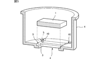
- FIG. 5 is a central longitudinally broken perspective view of the infrared sensor shown in Patent Document 2.
- This infrared sensor includes a rectangular plate-shaped optical filter 1 and a metal case 4 in which a rectangular opening window 2 that exposes the outer surface of the optical filter 1 to the outside is formed through a stepped portion 3. Yes. Then, the peripheral edge of the optical filter 1 is bonded and fixed to the inner surface of the step portion 3 with an adhesive. On the inner surface of the metal case 4, a recessed groove portion 10 opened at the inner surface of the step portion 3 is formed. These concave groove portions 10 guide the low-viscosity adhesive 5 applied on the inner surface of the metal case 4 toward the gap S sandwiched between the end surface of the optical filter 1 and the inner surface of the step portion 3.
- the adhesive 5 is introduced from the corner portion of the step portion 3. Is dropped into one concave groove 10, adhesive is introduced into two adjacent sides of the optical filter 1, and the optical filter 1 may be strongly attracted to the two adjacent sides and the optical filter 1 may tilt. is there.
- the above problem is not limited to the optical sensor with the can package structure. This is a problem that occurs in common with an optical sensor having a package structure in which an optical filter is attached to a metal case.
- An object of the present invention is to provide an optical sensor that suppresses the inclination that occurs when an optical filter is bonded, and a method for manufacturing the same, taking the above problem as a problem to be solved.
- the optical sensor according to the present invention includes an opening and a metal case provided with a bottom portion having a window portion facing the opening and having a step portion at a peripheral edge portion, and the step portion of the metal case.
- An optical filter bonded to the optical filter, and an optical element that receives light transmitted through the optical filter, and is connected to a plurality of locations in a gap formed between the step portion of the metal case and the peripheral portion of the optical filter.
- An adhesive guide groove is formed on the inner side (inner bottom surface) of the bottom surface of the metal case, and the gap is filled with an adhesive guided by the adhesive guide groove.
- the adhesive is guided to a plurality of locations in the gap formed between the step portion of the metal case and the peripheral portion of the optical filter, the adhesive is introduced into two adjacent sides. There is no risk of the optical filter being tilted and the optical filter is not inclined.
- interval is a rectangle along the periphery of the said window part by planar view, and the both ends of the said adhesive guide groove are connected to the corner part of the said gap
- the adhesive guide groove includes a first adhesive guide groove connected to adjacent first and second corner portions of the four corner portions of the gap, and adjacent third and fourth corners. It is preferable to include a second adhesive guide groove connected to the portion. With this structure, the adhesive is introduced from the four corners of the gap, so that the optical filter can be more effectively avoided.
- the adhesive guide groove has a V-shaped cross section or a U-shaped cross section. If it is this groove shape, there exists an effect that an adhesive agent will spread quickly by capillary action.
- An optical sensor manufacturing method includes an opening and a metal case that includes an opening and a bottom surface having a stepped portion that is opposed to the opening and has a stepped portion at the periphery.
- An optical sensor comprising: an optical filter bonded to the stepped portion; and an optical element that receives light transmitted through the optical filter, wherein the inner side (inner bottom surface) of the metal case has the Form an adhesive guide groove connected to a plurality of locations in the gap formed between the step portion of the metal case and the peripheral portion of the optical filter, and apply (drop) the adhesive to the center portion of the adhesive guide groove The gap is filled with an adhesive guided by the adhesive guide groove.
- the adhesive is simultaneously introduced into a plurality of locations in the gap formed between the step portion of the metal case and the peripheral portion of the optical filter, the adhesive is introduced into two adjacent sides. Therefore, there is no possibility that the optical filter is tilted and the optical filter is not tilted.
- the adhesive since the adhesive is guided to a plurality of locations in the gap formed between the step portion of the metal case and the peripheral portion of the optical filter, the adhesive is introduced into two adjacent sides.
- the optical filter is not attracted by, and the tilt of the optical filter can be prevented. Moreover, it can adhere more reliably with an appropriate amount of adhesive.
- FIG. 1A is a top view of a pyroelectric infrared sensor according to one embodiment of the present invention
- FIG. 1B is a cross-sectional view of a metal case with an optical filter of the pyroelectric infrared sensor
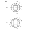
- 2A is a view seen from the opening 30A side of the metal case 30
- FIG. 2B is a view seen from the opening 30A side of the metal case with an optical filter to which the optical filter 28 is bonded
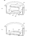
- 3A is a cutaway perspective view showing the bottom surface of the metal case 30 and the shape of the optical filter 28, and
- FIG. 3B is a cutaway perspective view of the metal case with an optical filter.
- FIG. 4 is an exploded perspective view of the entire pyroelectric infrared sensor.
- FIG. 5 is a central longitudinal cutaway perspective view of the infrared sensor disclosed in Patent Document 2.
- FIG. 5 is a central longitudinal cutaway perspective view of the infrared sensor disclosed in Patent Document 2.
- FIG. 1A is a top view of a pyroelectric infrared sensor according to one embodiment of the present invention
- FIG. 1B is a cross-sectional view of a metal case with an optical filter of the pyroelectric infrared sensor.
- the metal case 30 is a cylindrical metal case having an opening 30A and a bottom surface facing the opening 30A, and is a so-called round can case.
- the pyroelectric infrared sensor has a metal case 30 fixed and sealed to a stem on which various elements are arranged.
- FIG. 2A is a view seen from the opening 30A side of the metal case 30, and FIG. 2B is a view seen from the opening 30A side of the metal case with an optical filter to which the optical filter 28 is bonded.
- 3A is a cutaway perspective view showing the bottom surface of the metal case 30 and the shape of the optical filter 28, and FIG. 3B is a cutaway perspective view of the metal case with an optical filter.
- a window 30W is formed on the bottom surface 30B facing the opening 30A of the metal case 30.
- a step portion 30S is formed at the peripheral portion of the window portion 30W.
- the optical filter 28 is loosely fitted into the step portion 30S. That is, a gap P having a rectangular planar shape (rectangular shape along the periphery of the window 30W in plan view) is formed between the stepped portion 30S and the peripheral portion of the optical filter 28.
- the adhesive guide grooves 30G1 and 30G2 are formed on the bottom surface portion 30B of the metal case 30.
- the adhesive guide grooves 30G1 and 30G2 are formed on the metal case 30 so that the adhesive guide grooves 30G1 and 30G2 are connected to a plurality of locations in the gap P generated between the step portion 30S of the metal case 30 and the peripheral portion of the optical filter 28. It is formed on the bottom surface 30B.
- the first corner portion C1 and the second corner portion 2 adjacent to each other.
- the first adhesive guide groove 30G1 is connected to the corner portion C2.
- the second adhesive guiding groove 30G2 is connected to the adjacent third corner portion C3 and fourth corner portion C4.
- the adhesive guide grooves 30G1 and 30G2 have a V-shaped or U-shaped cross section, and the width thereof is, for example, 100 to 300 ⁇ m.
- the gap P is, for example, 50 to 150 ⁇ m.
- the optical filter 28 When joining the optical filter 28 to the bottom surface portion 30B of the metal case 30, the optical filter 28 is placed on the step portion 30S, and an adhesive is applied (dropped) to each of the adhesive guide grooves 30G1 and 30G2 with a dispenser. Since both ends of the adhesive guide groove 30G1 are connected to the gap P, and the adhesive guide groove 30G1 and the gap P communicate with each other, the adhesive applied (dropped) to the adhesive guide groove 30G1 is the adhesive guide groove. The adhesive flows into both ends of 30G1, and the adhesive is introduced into the gap P. The same applies to the adhesive guide groove 30G2. In this way, the adhesive guide grooves 30G1 and 30G2 and the gap P are evenly wetted with the adhesive throughout the entire area.
- the adjacent corner portions C1 and C2 of the gap P communicate with each other through the adhesive guide groove 30G1, and the adjacent corner portions C3 and C4 of the gap P communicate with each other through the adhesive guide groove 30G2, so that the gap P
- the adhesive thickness tends to be uniform over a wide range. Therefore, the surface tension applied to the optical filter 28 from the step portion 30 ⁇ / b> S via the adhesive is equally applied to the entire optical filter 28.
- the optical filter 28 is joined to the step portion 30S by solidifying the adhesive. Therefore, the optical filter 28 is bonded to the step portion 30S around the window portion 30W of the metal case without being inclined.
- the optical filter 28 is, for example, an AR-coated Si plate.
- the adhesive is, for example, a conductive adhesive and has a viscosity of about 20 to 110 Pa ⁇ S. If it is this viscosity range, it will be induced
- FIG. 1 A viscosity of about 20 to 110 Pa ⁇ S. If it is this viscosity range, it will be induced
- the adhesive is introduced from the corner portion of the gap formed between the step portion 30S of the metal case 30 and the peripheral portion of the optical filter 28, and the adhesive is applied along the rectangular groove. Since it spreads quickly, the drawing of the optical filter 28 can be avoided, and there is no fear that the optical filter tilts.
- the adhesive is simultaneously introduced into the adjacent corner portions, so that the optical filter 28 can be more effectively avoided. it can.
- the cross-sectional shape of the adhesive guide grooves 30G1 and 30G2 is V-shaped or U-shaped, that is, the capillary action acts strongly toward the bottom of the adhesive guide groove, the amount of application (dropping) of the adhesive is reduced. At least the adhesive is guided at the bottom of the adhesive guide grooves 30G1 and 30G2. And when there is much application
- the cross-sectional shape of the adhesive guide grooves 30G1 and 30G2 is V-shaped or U-shaped, there is an effect that the appropriate amount range of the adhesive to be applied (dropped) is wide.
- FIG. 4 is an exploded perspective view of the entire pyroelectric infrared sensor.
- the pyroelectric infrared sensor 101 includes a metal stem 12 and a metal case 30.
- the stem 12 includes a disk-shaped support base (stem base) 12a.
- three terminal pins 14a to 14c are formed penetrating the support base 12a in the thickness direction.
- the terminal pins 14a and 14b are attached to the support base 12a (hermetically sealed) through the glass material 16, and the terminal pin 14c is directly attached to the support base 12a.
- a hook-shaped member is formed to support the alumina substrate 20 by floating from the support base 12a.
- the FET 18 is attached to the lower surface of the alumina substrate 20.
- a plurality of predetermined electrode patterns 22 are formed on the alumina substrate 20.
- Each terminal of the FET 18 is electrically connected to each electrode pattern 22 of the alumina substrate 20.
- recesses 20a to 20c for fitting the terminal pins 14a to 14c are formed.
- the terminal pins 14a to 14c are fitted into the recesses 20a to 20c, and are electrically connected to and fixed to the electrode patterns 22 by a conductive paste or the like.
- a support base 24 having a substantially concave cross section is fixed to the upper surface of the alumina substrate 20.
- the support base 24 functions as a high resistance body for supporting the pyroelectric element 26 and obtaining an output voltage.
- the support table 24 is electrically connected to the corresponding electrode pattern 22 at both ends.
- the support 24 may be formed of a material such as borosilicate glass or alkali-free glass in that it has low thermal conductivity, mechanical strength, and a resistance value of about 10 11 ⁇ . preferable.
- a dual type pyroelectric element 26 is disposed on the upper surface of the support base 24. As described above, the window 30W is opened in the metal case 30, and the optical filter 28 is bonded to the window 30W.
- the pyroelectric element 26 is an “optical element” according to the present invention, and receives infrared light transmitted through the optical filter 28.
- the opening of the metal case 30 is resistance-welded to the outer peripheral portion of the support base portion 12a of the stem 12, whereby the inside of the package is sealed.
- cylindrical metal case 30 is shown.
- the present invention is not limited to this, and can be similarly applied to, for example, a rectangular parallelepiped metal case.
- the rectangular optical filter 28 is shown.
- the present invention is not limited to this, and for example, a disk-shaped optical filter can be similarly applied.
- the pyroelectric infrared sensor shown in the embodiment is an example, and it goes without saying that the present invention can be applied to various optical sensors in which an optical filter is bonded to a step portion of a metal case.
Landscapes
- Physics & Mathematics (AREA)
- General Physics & Mathematics (AREA)
- Spectroscopy & Molecular Physics (AREA)
- Engineering & Computer Science (AREA)
- Power Engineering (AREA)
- Optics & Photonics (AREA)
- Photometry And Measurement Of Optical Pulse Characteristics (AREA)
Abstract
金属ケース(30)の開口部(30A)に対向する底面部(30B)には窓部(30W)が形成されている。この窓部(30W)の周縁部には段差部(30S)が形成されている。光学フィルタ(28)は段差部(30S)に緩くはめ込まれ、段差部(30S)と光学フィルタ(28)の周縁部との間には平面形状が矩形の間隙(P)が生じる。金属ケース(30)の底面部(30B)には接着剤誘導溝(30G1,30G2)が形成されている。金属ケース(30)の段差部(30S)と光学フィルタ(28)の周縁部との間に生じる間隙(P)のうち二つのコーナー部に接着剤誘導溝(30G1)がつながるように接着剤誘導溝(30G1)が形成されている。この接着剤誘導溝(30G1)に接着剤を塗布することにより、接着剤誘導溝(30G1)で誘導された接着剤が間隙(P)に導入される。
Description
本発明は光学センサに関し、特に金属ケースに光学フィルタが取り付けられた光学センサおよびその製造方法に関する。
一般に光学センサは、所定波長を透過させる光学フィルタと、この光学フィルタを透過した光を受ける光学素子とを備える。パッケージ化された光学センサは、例えば特許文献1に示されているように、ステムと金属ケース(キャンケース)とを備え、光学素子がステムに取り付けられ、光学フィルタが金属ケースに取り付けられる。金属ケースへの光学フィルタの取り付け構造については例えば特許文献2に示されている。
図5は特許文献2に示されている赤外線センサの中央縦破断斜視図である。この赤外線センサは、矩形板状の光学フィルタ1と、この光学フィルタ1の外表面を外部に向かって露出させる矩形状開口窓2が段差部3を介して形成された金属ケース4とを備えている。そして、光学フィルタ1の周縁が段差部3の内側面に対して接着剤で接着固定される。金属ケース4の内表面上には段差部3の内側面で開口された凹溝部10が形成されている。これらの凹溝部10は金属ケース4の内表面上に塗布された低粘度の接着剤5を光学フィルタ1の端面と段差部3の内側面とで挟まれた隙間Sに向かって誘導する。
図5に示される構造の光学センサにおいては、段差部3の4つのコーナー部に凹溝部10がそれぞれ延びているので、接着剤5は段差部3のコーナー部から導入されるが、接着剤5は1つの凹溝部10に滴下された際に、光学フィルタ1の隣接する二つの辺に接着剤が導入され、隣接する二つの辺に光学フィルタ1が強く引き寄せられて光学フィルタ1が傾くおそれがある。
上記の問題は、キャンパッケージ構造の光学センサに限らない。光学フィルタが金属ケースに取り付けられるパッケージ構造の光学センサについて共通に生じる問題である。
本発明の目的は、上記問題を解決すべき課題と捉え、光学フィルタの接着時に生じる傾きを抑制した光学センサ、およびその製造方法を提供することにある。
(1)本発明の光学センサは、開口部と、この開口部に対向し、周縁部に段差部を有する窓部が形成された底面部とを備える金属ケースと、前記金属ケースの前記段差部に接着された光学フィルタと、前記光学フィルタを透過する光を受ける光学素子と、を備え、前記金属ケースの段差部と前記光学フィルタの周縁部との間に生じる間隙のうち複数の箇所につながる接着剤誘導溝が前記金属ケースの底面の内側(内底面)に形成されていて、前記間隙に前記接着剤誘導溝で誘導された接着剤が充填されたことを特徴とする。
上記構造によれば、金属ケースの段差部と光学フィルタの周縁部との間に生じる間隙のうち複数の箇所に接着剤が誘導されるので、隣接する二つの辺に接着剤が導入されることによる光学フィルタの引き寄せがなく、光学フィルタが傾くおそれがない。
(2)前記間隙は平面視で前記窓部の周縁に沿った矩形であり、前記接着剤誘導溝の両端は前記間隙のコーナー部につながっていることが好ましい。このことにより、間隙のコーナー部から接着剤が導入されるので、矩形状の溝に沿って接着剤が速やかに拡がり、光学フィルタの引き寄せがより効果的に回避できる。
(3)前記接着剤誘導溝は、前記間隙の4つのコーナー部のうち、隣接する第1・第2のコーナー部につながる第1の接着剤誘導溝、および隣接する第3・第4のコーナー部につながる第2の接着剤誘導溝を含むことが好ましい。この構造により、間隙の4つのコーナー部から接着剤が導入されるので、光学フィルタの引き寄せがより効果的に回避できる。
(4)前記接着剤誘導溝は断面V字状または断面U字状であることが好ましい。この溝形状であれば、毛管現象で接着剤が速やかに濡れ拡がるという効果を奏する。
(5)本発明の光学センサの製造方法は、開口部と、この開口部に対向し、周縁部に段差部を有する窓部が形成された底面部とを備える金属ケースと、前記金属ケースの前記段差部に接着された光学フィルタと、前記光学フィルタを透過する光を受ける光学素子と、を備えた光学センサの製造方法であって、前記金属ケースの底面の内側(内底面)に、前記金属ケースの段差部と前記光学フィルタの周縁部との間に生じる間隙のうち複数の箇所につながる接着剤誘導溝を形成し、前記接着剤誘導溝の中央部に接着剤を塗布(滴下)して、前記間隙に前記接着剤誘導溝で誘導された接着剤を充填することを特徴とする。
上記構造によれば、金属ケースの段差部と光学フィルタの周縁部との間に生じる間隙のうち複数の箇所に接着剤が同時に導入されるので、隣接する二つの辺に接着剤が導入されることによる光学フィルタの引き寄せがなく、光学フィルタが傾くおそれがない。
本発明によれば、金属ケースの段差部と光学フィルタの周縁部との間に生じる間隙のうち複数の箇所に接着剤が誘導されるので、隣接する二つの辺に接着剤が導入されることによる光学フィルタの引き寄せがなく、光学フィルタの傾きが防止できる。また、適正量の接着剤でより確実に接着できる。
図1(A)は本発明の一つの実施の形態である焦電型赤外線センサの上面図、図1(B)は焦電型赤外線センサの光学フィルタ付き金属ケースの断面図である。
金属ケース30は、開口部30Aと、この開口部30Aに対向する底面部とを有する円筒状の金属ケースであり、所謂丸型キャンケースである。後に示すように、焦電型赤外線センサは、各種素子が配置されたステムに金属ケース30が固着され、密封されたものである。
図2(A)は金属ケース30の開口部30A側から見た図、図2(B)は光学フィルタ28が接合された光学フィルタ付き金属ケースの開口部30A側から見た図である。図3(A)は金属ケース30の底面部および光学フィルタ28の形状を示す破断斜視図、図3(B)は光学フィルタ付き金属ケースの破断斜視図である。
金属ケース30の開口部30Aに対向する底面部30Bには窓部30Wが形成されている。この窓部30Wの周縁部には段差部30Sが形成されている。光学フィルタ28は段差部30Sに緩くはめ込まれる。すなわち、段差部30Sと光学フィルタ28の周縁部との間には平面形状が矩形の(平面視で窓部30Wの周縁に沿った矩形の)間隙Pが生じる。
金属ケース30の底面部30Bには接着剤誘導溝30G1,30G2が形成されている。
金属ケース30の段差部30Sと光学フィルタ28の周縁部との間に生じる間隙Pのうち複数の箇所に接着剤誘導溝30G1,30G2がつながるように接着剤誘導溝30G1,30G2が金属ケース30の底面部30Bに形成されている。図2(B)に示す例では、金属ケース30の段差部30Sと光学フィルタ28の周縁部との間に生じる間隙Pの4つのコーナー部のうち、隣接する第1のコーナー部C1および第2のコーナー部C2に第1の接着剤誘導溝30G1がつながっている。同様に、4つのコーナー部のうち、隣接する第3のコーナー部C3および第4のコーナー部C4に第2の接着剤誘導溝30G2がつながっている。
接着剤誘導溝30G1,30G2は断面V字状またはU字状であり、その幅は例えば100~300μmである。また、前記間隙Pは例えば50~150μmである。
金属ケース30の底面部30Bに光学フィルタ28を接合する際、段差部30Sに光学フィルタ28を載置し、接着剤誘導溝30G1,30G2のそれぞれにディスペンサで接着剤を塗布(滴下)する。接着剤誘導溝30G1の両端は間隙Pにつながっていて、接着剤誘導溝30G1と間隙Pは互いに連通しているので、接着剤誘導溝30G1に塗布(滴下)された接着剤は接着剤誘導溝30G1の両端にまで流れ、その接着剤が間隙Pに導入される。接着剤誘導溝30G2についても同様である。このように、接着剤誘導溝30G1,30G2および間隙Pは、その全体に亘って接着剤で均等に濡れる。また、間隙Pの隣接するコーナー部C1,C2は接着剤誘導溝30G1を介して連通し、間隙Pの隣接するコーナー部C3,C4は接着剤誘導溝30G2を介して連通するので、間隙Pの広い範囲に亘って接着剤の厚みは均等になりやすい。そのため、段差部30Sから接着剤を介して光学フィルタ28に掛かる表面張力は光学フィルタ28の全体に均等に掛かる。
その後、接着剤の固化により、光学フィルタ28は段差部30Sに接合される。そのため、光学フィルタ28は傾くことなく、金属ケースの窓部30W周囲の段差部30Sに接着される。
光学フィルタ28は例えばARコートされたSi板である。接着剤は、例えば導電性の接着剤であり、その粘度は20~110Pa・S程度である。この粘度範囲であれば、毛管現象により接着剤誘導溝30G1,30G2で誘導され、間隙Pに導入される。
上記構造と製造方法によれば、金属ケース30の段差部30Sと光学フィルタ28の周縁部との間に生じる間隙のうちコーナー部から接着剤が導入されて矩形状の溝に沿って接着剤が速やかに拡がるので、光学フィルタ28の引き寄せが回避でき、光学フィルタが傾くおそれがない。特に、接着剤誘導溝30G1,30G2のそれぞれの中央部に接着剤を塗布(滴下)することにより、隣接するコーナー部に接着剤が同時に導入されて、光学フィルタ28の引き寄せがより効果的に回避できる。
なお、接着剤誘導溝30G1,30G2の断面形状がV字状またはU字状であることにより、すなわち接着剤誘導溝の底部ほど毛管現象が強く作用するので、接着剤の塗布(滴下)量が少なくても接着剤は接着剤誘導溝30G1,30G2の底部で誘導される。そして、接着剤の塗布(滴下)量が多い場合には、接着剤の深さが深くなった状態で接着剤誘導溝30G1,30G2の表層部を流動する。いずれの場合でも接着剤は接着剤誘導溝30G1,30G2を誘導されることになる。このように接着剤誘導溝30G1,30G2の断面形状がV字状またはU字状であることで、塗布(滴下)すべき接着剤の適量範囲は広いという効果を奏する。
図4は焦電型赤外線センサ全体の分解斜視図である。焦電型赤外線センサ101は金属製のステム12および金属ケース30を含む。ステム12は円板状の支持台部(ステムベース)12aを含む。支持台部12aには、3本の端子ピン14a~14cが、支持台部12aを厚み方向に貫通して形成されている。このうち、端子ピン14a,14bは、ガラス材16を介して支持台部12aに取り付けられ(ハーメチックシールされ)ていて、端子ピン14cは支持台部12aに直接取り付けられている。端子ピン14a~14cのそれぞれの上端部近傍には、アルミナ基板20を支持台部12aから浮かせて支持するための鍔状部材が形成されている。
アルミナ基板20の下面にはFET18が取り付けられる。アルミナ基板20には、複数の所定の電極パターン22が形成される。そして、FET18の各端子はアルミナ基板20の各電極パターン22にそれぞれ電気的に接続される。アルミナ基板20の3つの角部近傍には、端子ピン14a~14cを嵌め込むための凹部20a~20cが形成されている。端子ピン14a~14cは、凹部20a~20cに嵌め込まれ、導電ペーストなどにより、各電極パターン22にそれぞれ電気的に接続され、かつ固着される。
アルミナ基板20の上面には、断面略凹字形状の支持台24が固着される。支持台24は焦電素子26を支持し且つ出力電圧を得るための高抵抗体として機能するものである。支持台24は、その両端部近傍が、それぞれ対応する電極パターン22と電気的に接続される。この支持台24としては、熱伝導度が低く、機械的強度があり、かつ、1011 Ω程度の抵抗値を有する点で、たとえばホウケイ酸ガラスや無アルカリガラスなどの材料で形成されることが好ましい。
支持台24の上面には、デュアル型の焦電素子26が配置されている。上述のとおり、金属ケース30には窓部30Wが開口されていて、この窓部30Wに光学フィルタ28が接着される。焦電素子26は本発明に係る「光学素子」であり、光学フィルタ28を透過する赤外光を受ける。
金属ケース30は、その開口部がステム12の支持台部12aの外周部に抵抗溶接されることにより、パッケージ内部が密封される。
なお、以上に示した実施形態では円筒状の金属ケース30を示したが、本発明はこれに限らず、例えば直方体状の金属ケースにも同様に適用できる。
また、以上に示した実施形態では矩形状の光学フィルタ28を示したが、本発明はこれに限らず、例えば円板状の光学フィルタであっても同様に適用できる。
また、実施形態で示した焦電型赤外線センサは一例であり、本発明は金属ケースの段差部に光学フィルタが接合された種々の光学センサに適用できることは言うまでもない。
C1~C4…コーナー部
P…間隙
12…ステム
12a…支持台部
14a,14b,14c…端子ピン
16…ガラス材
18…FET
20…アルミナ基板
22…電極パターン
24…支持台
26…焦電素子(光学素子)
28…光学フィルタ
30…金属ケース
30A…開口部
30B…底面部
101…焦電型赤外線センサ
30G1…第1の接着剤誘導溝
30G2…第2の接着剤誘導溝
30S…段差部
30W…窓部
P…間隙
12…ステム
12a…支持台部
14a,14b,14c…端子ピン
16…ガラス材
18…FET
20…アルミナ基板
22…電極パターン
24…支持台
26…焦電素子(光学素子)
28…光学フィルタ
30…金属ケース
30A…開口部
30B…底面部
101…焦電型赤外線センサ
30G1…第1の接着剤誘導溝
30G2…第2の接着剤誘導溝
30S…段差部
30W…窓部
Claims (5)
- 開口部と、この開口部に対向し、周縁部に段差部を有する窓部が形成された底面部とを備える金属ケースと、前記金属ケースの前記段差部に接着された光学フィルタと、前記光学フィルタを透過する光を受ける光学素子と、を備えた光学センサにおいて、
前記金属ケースの段差部と前記光学フィルタの周縁部との間に生じる間隙のうち複数の箇所につながる接着剤誘導溝が前記金属ケースの底面の内側に形成されていて、前記間隙に前記接着剤誘導溝で誘導された接着剤が充填されたことを特徴とする光学センサ。 - 前記間隙は平面視で前記窓部の周縁に沿った矩形であり、前記接着剤誘導溝の両端は前記間隙のコーナー部につながっている、請求項1に記載の光学センサ。
- 前記接着剤誘導溝は、前記間隙の4つのコーナー部のうち、隣接する第1・第2のコーナー部につながる第1の接着剤誘導溝、および隣接する第3・第4のコーナー部につながる第2の接着剤誘導溝を含む、請求項2に記載の光学センサ。
- 前記接着剤誘導溝は断面V字状または断面U字状である、請求項1~3のいずれかに記載の光学センサ。
- 開口部と、この開口部に対向し、周縁部に段差部を有する窓部が形成された底面部とを備える金属ケースと、前記金属ケースの前記段差部に接着された光学フィルタと、前記光学フィルタを透過する光を受ける光学素子と、を備えた光学センサの製造方法であって、
前記金属ケースの底面の内側に、前記金属ケースの段差部と前記光学フィルタの周縁部との間に生じる間隙のうち複数の箇所につながる接着剤誘導溝を形成し、前記接着剤誘導溝の中央部に接着剤を塗布して、前記間隙に前記接着剤誘導溝で誘導された接着剤を充填することを特徴とする光学センサの製造方法。
Priority Applications (1)
| Application Number | Priority Date | Filing Date | Title |
|---|---|---|---|
| JP2014524703A JPWO2014010370A1 (ja) | 2012-07-10 | 2013-06-17 | 光学センサおよびその製造方法 |
Applications Claiming Priority (2)
| Application Number | Priority Date | Filing Date | Title |
|---|---|---|---|
| JP2012-154561 | 2012-07-10 | ||
| JP2012154561 | 2012-07-10 |
Publications (1)
| Publication Number | Publication Date |
|---|---|
| WO2014010370A1 true WO2014010370A1 (ja) | 2014-01-16 |
Family
ID=49915838
Family Applications (1)
| Application Number | Title | Priority Date | Filing Date |
|---|---|---|---|
| PCT/JP2013/066544 Ceased WO2014010370A1 (ja) | 2012-07-10 | 2013-06-17 | 光学センサおよびその製造方法 |
Country Status (2)
| Country | Link |
|---|---|
| JP (1) | JPWO2014010370A1 (ja) |
| WO (1) | WO2014010370A1 (ja) |
Citations (7)
| Publication number | Priority date | Publication date | Assignee | Title |
|---|---|---|---|---|
| JPH09159525A (ja) * | 1995-12-12 | 1997-06-20 | Murata Mfg Co Ltd | 赤外線センサ |
| JPH10166581A (ja) * | 1996-12-06 | 1998-06-23 | Seiko Epson Corp | インクジェット式記録ヘッド、及びその製造方法 |
| JP2004334048A (ja) * | 2003-05-09 | 2004-11-25 | Sony Corp | 光学装置、レンズ鏡筒及び撮像装置 |
| JP2005240548A (ja) * | 2004-02-26 | 2005-09-08 | Getzner Werkstoffe Holding Gmbh | 床の床パネルを弾性的に支持する支持脚 |
| JP2007264115A (ja) * | 2006-03-27 | 2007-10-11 | Mitsumi Electric Co Ltd | カメラモジュール |
| JP2011000648A (ja) * | 2009-06-16 | 2011-01-06 | Chugoku Electric Power Co Inc:The | 軸部材抜き取り工具及び軸部材抜き取り方法 |
| JP2011112998A (ja) * | 2009-11-30 | 2011-06-09 | Seiko Epson Corp | 干渉フィルター、測色センサー、測色モジュール、及び干渉フィルターの製造方法 |
-
2013
- 2013-06-17 WO PCT/JP2013/066544 patent/WO2014010370A1/ja not_active Ceased
- 2013-06-17 JP JP2014524703A patent/JPWO2014010370A1/ja active Pending
Patent Citations (7)
| Publication number | Priority date | Publication date | Assignee | Title |
|---|---|---|---|---|
| JPH09159525A (ja) * | 1995-12-12 | 1997-06-20 | Murata Mfg Co Ltd | 赤外線センサ |
| JPH10166581A (ja) * | 1996-12-06 | 1998-06-23 | Seiko Epson Corp | インクジェット式記録ヘッド、及びその製造方法 |
| JP2004334048A (ja) * | 2003-05-09 | 2004-11-25 | Sony Corp | 光学装置、レンズ鏡筒及び撮像装置 |
| JP2005240548A (ja) * | 2004-02-26 | 2005-09-08 | Getzner Werkstoffe Holding Gmbh | 床の床パネルを弾性的に支持する支持脚 |
| JP2007264115A (ja) * | 2006-03-27 | 2007-10-11 | Mitsumi Electric Co Ltd | カメラモジュール |
| JP2011000648A (ja) * | 2009-06-16 | 2011-01-06 | Chugoku Electric Power Co Inc:The | 軸部材抜き取り工具及び軸部材抜き取り方法 |
| JP2011112998A (ja) * | 2009-11-30 | 2011-06-09 | Seiko Epson Corp | 干渉フィルター、測色センサー、測色モジュール、及び干渉フィルターの製造方法 |
Also Published As
| Publication number | Publication date |
|---|---|
| JPWO2014010370A1 (ja) | 2016-06-20 |
Similar Documents
| Publication | Publication Date | Title |
|---|---|---|
| JP6564206B2 (ja) | 発光装置 | |
| CN105683725B (zh) | 光检测装置 | |
| JP4107347B2 (ja) | 赤外線センサおよび赤外線センサの製造方法 | |
| JP6214631B2 (ja) | ファブリー・ペロー干渉計およびその製造方法 | |
| US10066995B2 (en) | Light-detecting device | |
| JP2016206458A (ja) | 光学装置および光学装置の製造方法 | |
| JP6528643B2 (ja) | 波長多重光通信モジュール | |
| TW201505434A (zh) | 相機模組 | |
| ITMI20130520A1 (it) | Realizzazione di un dissipatore di calore tramite saldatura ad onda | |
| EP1887331A1 (en) | Infrared sensor and its manufacturing process | |
| CN104333679B (zh) | 相机模组 | |
| JP6487626B2 (ja) | 半導体装置 | |
| JP5790878B2 (ja) | 水晶振動子 | |
| WO2014010370A1 (ja) | 光学センサおよびその製造方法 | |
| JP2014062747A (ja) | 流体取扱装置 | |
| US10705064B2 (en) | Micro sensor package | |
| US20140029223A1 (en) | Circuit board with reduced adhesive overflow and circuit structure thereof | |
| JP6383147B2 (ja) | パッケージ | |
| JP5922606B2 (ja) | 光スイッチモジュール | |
| US10573677B2 (en) | Semiconductor device on which a transparent plate is disposed for exposing an element region | |
| JP2013079895A (ja) | 半導体物理量センサ | |
| JP5755114B2 (ja) | 素子収納用パッケージおよび光半導体装置 | |
| JP7155659B2 (ja) | 気密パッケージ及び気密パッケージの製造方法 | |
| JP2004264836A (ja) | ファイバ加熱用デバイス、およびその製造方法 | |
| JP2004228027A (ja) | チップ型ヒューズおよびその製造方法 |
Legal Events
| Date | Code | Title | Description |
|---|---|---|---|
| 121 | Ep: the epo has been informed by wipo that ep was designated in this application |
Ref document number: 13816964 Country of ref document: EP Kind code of ref document: A1 |
|
| ENP | Entry into the national phase |
Ref document number: 2014524703 Country of ref document: JP Kind code of ref document: A |
|
| NENP | Non-entry into the national phase |
Ref country code: DE |
|
| 122 | Ep: pct application non-entry in european phase |
Ref document number: 13816964 Country of ref document: EP Kind code of ref document: A1 |