WO2014003164A1 - アンテナ装置、給電素子および通信端末装置 - Google Patents
アンテナ装置、給電素子および通信端末装置 Download PDFInfo
- Publication number
- WO2014003164A1 WO2014003164A1 PCT/JP2013/067805 JP2013067805W WO2014003164A1 WO 2014003164 A1 WO2014003164 A1 WO 2014003164A1 JP 2013067805 W JP2013067805 W JP 2013067805W WO 2014003164 A1 WO2014003164 A1 WO 2014003164A1
- Authority
- WO
- WIPO (PCT)
- Prior art keywords
- coil
- antenna device
- power feeding
- conductor
- feeding element
- Prior art date
- Legal status (The legal status is an assumption and is not a legal conclusion. Google has not performed a legal analysis and makes no representation as to the accuracy of the status listed.)
- Ceased
Links
Images









Classifications
-
- H—ELECTRICITY
- H01—ELECTRIC ELEMENTS
- H01Q—ANTENNAS, i.e. RADIO AERIALS
- H01Q1/00—Details of, or arrangements associated with, antennas
- H01Q1/12—Supports; Mounting means
- H01Q1/22—Supports; Mounting means by structural association with other equipment or articles
- H01Q1/24—Supports; Mounting means by structural association with other equipment or articles with receiving set
- H01Q1/241—Supports; Mounting means by structural association with other equipment or articles with receiving set used in mobile communications, e.g. GSM
- H01Q1/242—Supports; Mounting means by structural association with other equipment or articles with receiving set used in mobile communications, e.g. GSM specially adapted for hand-held use
- H01Q1/243—Supports; Mounting means by structural association with other equipment or articles with receiving set used in mobile communications, e.g. GSM specially adapted for hand-held use with built-in antennas
-
- H—ELECTRICITY
- H01—ELECTRIC ELEMENTS
- H01Q—ANTENNAS, i.e. RADIO AERIALS
- H01Q7/00—Loop antennas with a substantially uniform current distribution around the loop and having a directional radiation pattern in a plane perpendicular to the plane of the loop
-
- H—ELECTRICITY
- H01—ELECTRIC ELEMENTS
- H01Q—ANTENNAS, i.e. RADIO AERIALS
- H01Q1/00—Details of, or arrangements associated with, antennas
- H01Q1/12—Supports; Mounting means
- H01Q1/22—Supports; Mounting means by structural association with other equipment or articles
- H01Q1/2208—Supports; Mounting means by structural association with other equipment or articles associated with components used in interrogation type services, i.e. in systems for information exchange between an interrogator/reader and a tag/transponder, e.g. in Radio Frequency Identification [RFID] systems
-
- G—PHYSICS
- G06—COMPUTING OR CALCULATING; COUNTING
- G06K—GRAPHICAL DATA READING; PRESENTATION OF DATA; RECORD CARRIERS; HANDLING RECORD CARRIERS
- G06K19/00—Record carriers for use with machines and with at least a part designed to carry digital markings
- G06K19/06—Record carriers for use with machines and with at least a part designed to carry digital markings characterised by the kind of the digital marking, e.g. shape, nature, code
- G06K19/067—Record carriers with conductive marks, printed circuits or semiconductor circuit elements, e.g. credit or identity cards also with resonating or responding marks without active components
- G06K19/07—Record carriers with conductive marks, printed circuits or semiconductor circuit elements, e.g. credit or identity cards also with resonating or responding marks without active components with integrated circuit chips
- G06K19/0723—Record carriers with conductive marks, printed circuits or semiconductor circuit elements, e.g. credit or identity cards also with resonating or responding marks without active components with integrated circuit chips the record carrier comprising an arrangement for non-contact communication, e.g. wireless communication circuits on transponder cards, non-contact smart cards or RFIDs
- G06K19/0727—Record carriers with conductive marks, printed circuits or semiconductor circuit elements, e.g. credit or identity cards also with resonating or responding marks without active components with integrated circuit chips the record carrier comprising an arrangement for non-contact communication, e.g. wireless communication circuits on transponder cards, non-contact smart cards or RFIDs the arrangement being a circuit facilitating integration of the record carrier with a hand-held device such as a smart phone of PDA
-
- G—PHYSICS
- G06—COMPUTING OR CALCULATING; COUNTING
- G06K—GRAPHICAL DATA READING; PRESENTATION OF DATA; RECORD CARRIERS; HANDLING RECORD CARRIERS
- G06K19/00—Record carriers for use with machines and with at least a part designed to carry digital markings
- G06K19/06—Record carriers for use with machines and with at least a part designed to carry digital markings characterised by the kind of the digital marking, e.g. shape, nature, code
- G06K19/067—Record carriers with conductive marks, printed circuits or semiconductor circuit elements, e.g. credit or identity cards also with resonating or responding marks without active components
- G06K19/07—Record carriers with conductive marks, printed circuits or semiconductor circuit elements, e.g. credit or identity cards also with resonating or responding marks without active components with integrated circuit chips
- G06K19/077—Constructional details, e.g. mounting of circuits in the carrier
- G06K19/07749—Constructional details, e.g. mounting of circuits in the carrier the record carrier being capable of non-contact communication, e.g. constructional details of the antenna of a non-contact smart card
- G06K19/0775—Constructional details, e.g. mounting of circuits in the carrier the record carrier being capable of non-contact communication, e.g. constructional details of the antenna of a non-contact smart card arrangements for connecting the integrated circuit to the antenna
- G06K19/07756—Constructional details, e.g. mounting of circuits in the carrier the record carrier being capable of non-contact communication, e.g. constructional details of the antenna of a non-contact smart card arrangements for connecting the integrated circuit to the antenna the connection being non-galvanic, e.g. capacitive
-
- G—PHYSICS
- G06—COMPUTING OR CALCULATING; COUNTING
- G06K—GRAPHICAL DATA READING; PRESENTATION OF DATA; RECORD CARRIERS; HANDLING RECORD CARRIERS
- G06K19/00—Record carriers for use with machines and with at least a part designed to carry digital markings
- G06K19/06—Record carriers for use with machines and with at least a part designed to carry digital markings characterised by the kind of the digital marking, e.g. shape, nature, code
- G06K19/067—Record carriers with conductive marks, printed circuits or semiconductor circuit elements, e.g. credit or identity cards also with resonating or responding marks without active components
- G06K19/07—Record carriers with conductive marks, printed circuits or semiconductor circuit elements, e.g. credit or identity cards also with resonating or responding marks without active components with integrated circuit chips
- G06K19/077—Constructional details, e.g. mounting of circuits in the carrier
- G06K19/07749—Constructional details, e.g. mounting of circuits in the carrier the record carrier being capable of non-contact communication, e.g. constructional details of the antenna of a non-contact smart card
- G06K19/07773—Antenna details
- G06K19/07794—Antenna details the record carrier comprising a booster or auxiliary antenna in addition to the antenna connected directly to the integrated circuit
-
- G—PHYSICS
- G06—COMPUTING OR CALCULATING; COUNTING
- G06K—GRAPHICAL DATA READING; PRESENTATION OF DATA; RECORD CARRIERS; HANDLING RECORD CARRIERS
- G06K7/00—Methods or arrangements for sensing record carriers, e.g. for reading patterns
- G06K7/10—Methods or arrangements for sensing record carriers, e.g. for reading patterns by electromagnetic radiation, e.g. optical sensing; by corpuscular radiation
- G06K7/10009—Methods or arrangements for sensing record carriers, e.g. for reading patterns by electromagnetic radiation, e.g. optical sensing; by corpuscular radiation sensing by radiation using wavelengths larger than 0.1 mm, e.g. radio-waves or microwaves
-
- H—ELECTRICITY
- H01—ELECTRIC ELEMENTS
- H01F—MAGNETS; INDUCTANCES; TRANSFORMERS; SELECTION OF MATERIALS FOR THEIR MAGNETIC PROPERTIES
- H01F17/00—Fixed inductances of the signal type
- H01F17/0006—Printed inductances
- H01F17/0013—Printed inductances with stacked layers
-
- H—ELECTRICITY
- H01—ELECTRIC ELEMENTS
- H01F—MAGNETS; INDUCTANCES; TRANSFORMERS; SELECTION OF MATERIALS FOR THEIR MAGNETIC PROPERTIES
- H01F19/00—Fixed transformers or mutual inductances of the signal type
- H01F19/04—Transformers or mutual inductances suitable for handling frequencies considerably beyond the audio range
-
- H—ELECTRICITY
- H01—ELECTRIC ELEMENTS
- H01Q—ANTENNAS, i.e. RADIO AERIALS
- H01Q1/00—Details of, or arrangements associated with, antennas
- H01Q1/44—Details of, or arrangements associated with, antennas using equipment having another main function to serve additionally as an antenna, e.g. means for giving an antenna an aesthetic aspect
-
- H—ELECTRICITY
- H01—ELECTRIC ELEMENTS
- H01Q—ANTENNAS, i.e. RADIO AERIALS
- H01Q1/00—Details of, or arrangements associated with, antennas
- H01Q1/48—Earthing means; Earth screens; Counterpoises
-
- H—ELECTRICITY
- H01—ELECTRIC ELEMENTS
- H01Q—ANTENNAS, i.e. RADIO AERIALS
- H01Q1/00—Details of, or arrangements associated with, antennas
- H01Q1/52—Means for reducing coupling between antennas; Means for reducing coupling between an antenna and another structure
-
- H—ELECTRICITY
- H01—ELECTRIC ELEMENTS
- H01Q—ANTENNAS, i.e. RADIO AERIALS
- H01Q1/00—Details of, or arrangements associated with, antennas
- H01Q1/52—Means for reducing coupling between antennas; Means for reducing coupling between an antenna and another structure
- H01Q1/521—Means for reducing coupling between antennas; Means for reducing coupling between an antenna and another structure reducing the coupling between adjacent antennas
-
- H—ELECTRICITY
- H01—ELECTRIC ELEMENTS
- H01Q—ANTENNAS, i.e. RADIO AERIALS
- H01Q23/00—Antennas with active circuits or circuit elements integrated within them or attached to them
-
- H—ELECTRICITY
- H01—ELECTRIC ELEMENTS
- H01Q—ANTENNAS, i.e. RADIO AERIALS
- H01Q7/00—Loop antennas with a substantially uniform current distribution around the loop and having a directional radiation pattern in a plane perpendicular to the plane of the loop
- H01Q7/06—Loop antennas with a substantially uniform current distribution around the loop and having a directional radiation pattern in a plane perpendicular to the plane of the loop with core of ferromagnetic material
Definitions
- the present invention relates to an antenna device, a feed element, and a communication terminal device used in a communication system of HF band or UHF band.
- an IC chip for RFID and a matching element are mainly mounted on a printed wiring board, and an antenna. Is affixed to the inside of the terminal housing, and the IC chip for RFID and the antenna are electrically (directly) connected via a spring pin or the like.
- this connection method there is a problem that contact failure occurs due to wear of the contact portion or displacement during assembly.
- a reader / writer structure including an antenna substrate provided with a loop antenna and a control substrate provided with a transmission / reception circuit is disclosed (see Patent Document 1).
- the loop antenna and the transmission / reception circuit are electrically connected by magnetically coupling the coil provided on the control board and the loop antenna. Thereby, there is no physical contact portion, and the occurrence of contact failure can be prevented.
- An object of the present invention is to provide an antenna device, a feed element, and a communication terminal device including the antenna device that can suppress variation in the degree of coupling and can also prevent problems such as interference with surrounding components.
- the antenna device of the present invention A conductor member and a power feeding element that feeds a high-frequency signal to the conductor member;
- the power feeding element includes a first coil connected to a power feeding circuit, a second coil magnetically coupled to the first coil, and two terminal electrodes that connect the second coil to the conductor member. It is characterized by being provided integrally with the body.
- the power feeding element preferably includes a capacitor connected between at least one of the two terminal electrodes and at least one terminal of the second coil.
- the conductor member is a conductor film formed on a substrate, and the substrate includes a terminal to which at least one of the two terminal electrodes of the feeding element is connected, It is preferable that a capacitor connected between the terminal and the conductor member is provided.
- the conductor member, the capacitor, and the first coil constitute a resonance circuit.
- the capacitance of the capacitor and the inductance of the first coil are determined so that the resonance frequency of the resonance circuit is equal to or close to the communication frequency.
- the inductance of the second coil is smaller than an inductance component of the conductor member viewed from the two terminal electrodes.
- the said conductor member is provided with the slit or opening which penetrates into an inside from an edge, and the said two terminal electrodes are arrange
- the power feeding element is preferably a laminated structure in which a plurality of insulator layers on which conductors forming the first coil and the second coil are formed are laminated.
- the power feeding element includes a plurality of insulator layers formed with conductors forming the first coil and the second coil, and a plurality of insulator layers formed with conductors forming the capacitor. It is preferable.
- the conductor film is preferably a ground electrode or a shield electrode of a circuit formed on the substrate.
- the power feeding circuit has an RFIC, and the RFIC is mounted on the insulator body.
- the feeding element of the present invention is Used together with conductor members to configure the antenna device, A first coil provided with an insulator body, connected to a power feeding circuit, a second coil magnetically coupled to the first coil, and two terminal electrodes connecting the second coil to the conductor member, It is formed integrally with an insulator body.
- the communication terminal device of the present invention An antenna device and a power feeding circuit connected to the antenna device;
- the antenna device is A conductor member and a power feeding element that feeds a high-frequency signal to the conductor member;
- the power feeding element includes a first coil connected to a power feeding circuit, a second coil magnetically coupled to the first coil, and two terminal electrodes that connect the second coil to the conductor member. It is characterized by being provided integrally with the body.
- the first coil and the second coil are magnetically coupled by the insulating element body, thereby suppressing the influence due to coupling to the outside of the feed element compared to the case of coupling between different element bodies. can do. Further, by combining with one element body, the coupling degree does not change according to the mounting variation of the feeding elements, and the variation in antenna characteristics due to the change in coupling degree can be suppressed.
- FIG. 1 is a plan view of an antenna device 101 according to the first embodiment.
- FIG. 2 is an exploded perspective view of the power feeding element 36 according to the first embodiment.
- FIG. 3 is a diagram for explaining the radiation of the magnetic field of the antenna device 101 according to the first embodiment.
- FIG. 4 is an equivalent circuit diagram of the antenna device 101 including the power feeding circuit.
- FIG. 5 is a plan view of the antenna device 102 according to the second embodiment.
- FIG. 6 is a plan view of the antenna device 103 according to the third embodiment.
- FIG. 7 is an exploded perspective view of the power feeding element 37 according to the fourth embodiment.
- FIG. 8 is a plan view of the antenna device 104A on which the feed element 37 shown in FIG. 7 is mounted.
- FIG. 9 is a plan view of an antenna device 104B different from the antenna device shown in FIG.
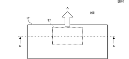
- FIG. 10 is a plan view of an antenna device 105 according to the fifth embodiment.
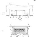
- FIG. 11 is a sectional view taken along line XX in FIG.
- FIG. 12A is a top view of the antenna device 106 according to the sixth embodiment, and
- FIG. 12B is a cross-sectional view.
- FIG. 13 is a plan view of an antenna device 107 according to the seventh embodiment.
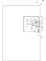
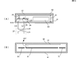
- FIG. 14 is a plan view showing the structure inside the housing of the communication terminal apparatus according to the eighth embodiment.
- 15A is a cross-sectional view in the short side direction of the communication terminal device shown in FIG. 14, and
- FIG. 15B is a cross-sectional view in the long side direction of the communication terminal device.
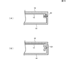
- FIGS. 16A and 16B are diagrams illustrating an example of a joint structure between an upper housing and a lower housing.
- FIG. 17 is a plan view showing the structure inside the
- the antenna devices of some embodiments described below are antenna devices for transmitting and receiving HF band (such as 13.56 MHz band) high-frequency signals provided in communication terminals typified by smartphones and tablet terminals.
- HF band such as 13.56 MHz band
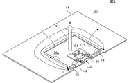
- FIG. 1 is a plan view of an antenna device 101 according to the first embodiment.
- FIG. 2 is an exploded perspective view of the power feeding element 36 according to the first embodiment.
- FIG. 3 is a diagram for explaining the radiation of the magnetic field of the antenna device 101 according to the first embodiment.
- the outer shape of the power feeding element 36 is shown, and the first coil L21 and the second coil L22 included therein are indicated by circuit symbols.
- the antenna device 101 includes a conductor surface 14 as a conductor member.
- a rectangular opening 14 ⁇ / b> A is formed in the conductor surface 14.
- the conductor surface 14 is, for example, a ground conductor pattern of a circuit board, and the opening 14A is, for example, a non-conductor portion where the ground conductor pattern of the circuit board is not formed.
- the opening 14 ⁇ / b> A is not a closed opening, and an open portion is formed so that a part thereof communicates with the outside of the conductor surface 14.
- a first mounting portion 141 and a second mounting portion 142 for mounting the power feeding element 36 are formed in the open portion.
- the first mounting portion 141 is directly connected to the conductor surface 14.
- the first mounting portion 141 may be integrated with the conductor surface 14, or may be a separate member from the conductor surface 14, and may be connected to the conductor surface 14 by a wire, a connection portion including a chip inductor, or the like. It may be connected.
- the second mounting portion 142 is isolated from the conductor surface 14 and the first mounting portion 141, and is connected to the conductor surface 14 via the capacitor C3.
- the power feeding element 36 has a first coil L21 and a second coil L22 that are mainly coupled via a magnetic field, as will be described in detail later.
- a first end of the second coil L22 is connected to the first mounting part 141, and a second end of the second coil L22 is connected to the second mounting part 142.
- the open part of the opening 14A is closed by the capacitor C3, the second coil L22, etc., and the opening 14A constitutes a loop.
- a resonance circuit is formed by the inductance component of the loop, the second coil L22, and the capacitor C3.
- the first mounting portion 141 may be connected to the conductor surface 14 via a capacitor. By providing this capacitor, the resonance frequency of the formed resonance circuit can be adjusted.
- the power feeding element 36 is a component having an insulator as a base body, and is a laminated structure in which a plurality of insulator layers 361a, 361b, 361c, and 361d are laminated.
- the insulator layers 361a and 361d are nonmagnetic layers made of a nonmagnetic ferrite sheet or the like
- the insulator layers 361b and 361c are magnetic layers made of a magnetic ferrite sheet or the like.
- the feeding element 36 includes a first coil L21 and a second coil L22 that are magnetically coupled.
- the magnetic layer 361b includes coil conductor patterns 362a and 362b that form the first coil L21, and an insulator layer.
- Coil conductor patterns 363a and 363b that form the second coil L22 are formed on 361d.
- the coil conductor patterns 362a and 362b and the coil conductor patterns 363a and 363b are formed such that the coil winding axis is perpendicular to the stacking direction.
- linear coil conductor patterns 362a and 362b are alternately formed on the magnetic layer 361b, and linear coil conductor patterns 363a and 363b are alternately formed on the insulator layer 361d.
- via conductors for connecting the coil conductor patterns 362a and 362b and the coil conductor patterns 363a and 363b are formed.
- the first coil L21 and the second coil L22 are formed with the coil openings coincident.
- Terminal electrodes P1, P2, P3, and P4 are formed on the lower surface of the insulator layer 361d.
- the terminal electrode P1 is connected to one end of the outermost conductor pattern of the coil conductor pattern 363b via a via conductor.
- the terminal electrode P2 is connected to one end of the outermost conductor pattern of the coil conductor pattern 362a via a via conductor.
- the terminal electrode P3 is connected to one end of the outermost conductor pattern of the coil conductor pattern 362b via a via conductor.
- the terminal electrode P4 is connected to one end of the outermost conductor pattern of the coil conductor pattern 363a via a via conductor.
- FIG. 2 shows an example in which two magnetic layers are provided, a plurality of magnetic layers may be further laminated.
- a plurality of magnetic layers 361c may be stacked.
- the opening 14A is formed with power supply circuit side mounting portions 611 and 612 to which the first end and the second end of the first coil L21 are respectively connected.
- a capacitor C4 is connected between the power supply circuit side mounting portions 611 and 612.
- the RFIC 60 is connected to the power feeding circuit side mounting portions 611 and 612.
- the RFIC 60 constitutes a power feeding circuit.
- the RFIC 60 is configured as a semiconductor chip component.
- the first coil L21 and the second coil L22 of the power feeding element 36 are magnetically coupled.
- a power feeding circuit is connected to the first coil L21, and when the two coils L21 and L22 are magnetically coupled, a current i flows along the opening 14A of the loop as shown in FIGS. .
- the opening 14A functions as a radiating portion as shown in FIG. Therefore, the antenna device 101 points in the direction of arrow A in FIG.
- FIG. 4 is an equivalent circuit diagram of the antenna device 101 including the feeding circuit.
- the first coil L21 and the capacitor C4 constitute a resonance circuit on the power feeding circuit side.
- the inductor L23 in the figure corresponds to the inductance of the opening 14A of the loop, and forms a resonance circuit on the radiation element side together with the second coil L22 and the capacitor C3.
- this embodiment has a great influence on a UHF band antenna that obtains antenna characteristics using a housing current such as a main antenna. If the size of the magnetic material can be reduced as described above, the influence can be reduced. Further, a ferrite member or the like for preventing unnecessary radiation from the power feeding element 36 to the outside is not required, and the other high-frequency antenna (such as a cellular antenna) or the first connection portion 21 described in the first embodiment or the like. The degree of freedom of arrangement is improved without considering the positional relationship.
- the following effects can be obtained by using the power supply element 36 having a transformer coupling structure as shown in the present embodiment.
- the first coil L21 is formed on a magnetic layer such as ferrite, it is not easily affected by the surroundings. That is, unnecessary coupling with an external circuit is unlikely to occur, unnecessary radiation is suppressed, and interference from the external circuit is also suppressed.
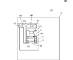
- FIG. 5 is a plan view of the antenna device 102 according to the second embodiment.
- the conductor surface 15 has two openings 15 ⁇ / b> A and 15 ⁇ / b> B that have an open portion and are not closed. Between opening 15A, 15B, the 1st mounting part 151 to which the 1st end of the 2nd coil L22 of the electric power feeding element 36 is connected and the 2nd mounting part 152 to which a 2nd end is connected are formed. Yes.
- the first mounting portion 151 is connected to the conductor surface 15 directly or indirectly (for example, via a capacitor).
- the first mounting portion 151 may be integrated with the conductor surface 15, or may be formed of a separate member from the conductor surface 15, and this separate member may be connected to the conductor surface 15.
- the second mounting portion 152 is formed separately from the first mounting portion 151 and the conductor surface 15.
- a capacitor C3 is connected between the second mounting part 152 and the conductor surface 15.
- a second coil L22 is connected between the second mounting part 152 and the first mounting part 151. Therefore, the opening 15A forms a loop by closing the open portion by the capacitor C3 and the second coil L22.
- a resonance circuit is configured by the loop inductance, the capacitor C3, and the second coil L22.
- feeding circuit side mounting portions 611 and 612 are formed, and a capacitor C4 is connected to the feeding circuit side mounting portions 611 and 612.
- the first end and the second end of the first coil L21 of the power feeding element 36 are connected to the power feeding circuit side mounting portions 611 and 612, respectively.
- the feeding circuit is formed in the opening 14A serving as the radiating portion, whereas in the antenna device 102 of the present embodiment, an opening different from the opening 15A serving as the radiating portion. Since the power feeding circuit is configured in 15B, the radiation efficiency can be increased.
- FIG. 6 is a plan view of the antenna device 103 according to the third embodiment.
- two openings 16A and 16B are formed in the conductor surface 16 as in FIG.
- a first mounting portion 161 to which the first end of the second coil L22 of the power feeding element 36 is connected and a second mounting portion 162 to which the second end is connected are formed between the openings 16A and 16B. Yes.
- the first mounting portion 161 is connected to the conductor surface 16 directly or indirectly.
- a capacitor C3 is connected between the second mounting portion 162 and the conductor surface 16.
- the opening 16A has an L-shaped shape with a rectangular portion extending in one direction. Accordingly, in addition to the effect described in the antenna device 102 of FIG. 5, since the magnetic field is radiated from the extended portion, the radiation range of the magnetic field can be widened.
- an actual component capacitor C3 is mounted on the conductor surface in order to form a resonance circuit, whereas in the fourth mounting embodiment, the feed element has a built-in capacitor. Yes.
- FIG. 7 is an exploded perspective view of the power feeding element 37 according to the fourth embodiment.
- the power feeding element 37 has a laminated structure having a plurality of insulator layers 371a to 371g. Specifically, the insulator layers 371b and 371c are magnetic layers, and the other layers are nonmagnetic layers. As described with reference to FIG. 2, conductor patterns that form the first coil L21 and the second coil L22 are formed on the insulating layers 371b and 371d in the stacking direction. Also, each element constituting the matching circuit on the power feeding circuit side including the RFIC 60 and the capacitor C4 is mounted on the uppermost insulator layer 371a in the stacking direction. The matching circuit is connected to the first end and the second end of the first coil L21.
- a flat conductor pattern 373a is formed on the insulator layer 371e below the layer on which the first coil L21 and the second coil L22 are formed, and a flat conductor pattern 373b is formed on the insulator layer 371f.
- the flat conductor patterns 373a and 373b constitute a capacitor.
- terminal conductor patterns 372a and 372b serving as external terminals are formed on the lowermost insulator layer 371g.
- the first end of the second coil L22 is connected to the flat conductor pattern 373a through, for example, a via conductor, and the flat conductor pattern 373b is connected to the terminal conductor pattern 372b.
- the second end of the second coil L22 is connected to the terminal conductor pattern 372a.
- FIG. 8 is a plan view of the antenna device 104A on which the feed element 37 shown in FIG. 7 is mounted.
- the antenna device 104 ⁇ / b> A includes a conductor surface 17.
- the conductor surface 17 is formed with an opening 17A that is partially open.
- the conductor surface 17 has the first mounting portion 171 to which the terminal conductor pattern 372a of the power feeding element 37 is connected and the second mounting portion 172 to which the terminal conductor pattern 372b of the power feeding element 37 is connected across the open portion. And have.
- the feeding element 37 has a built-in capacitor. For this reason, by mounting the power feeding element 37 on the conductor surface 17, a resonance circuit is configured by the capacitor of the power feeding element 37, the inductance of the second coil L22, and the opening 17A. That is, the actual capacitor is not necessary on the conductor surface 17 in order to form a resonance circuit. Further, since the RFIC 60, the capacitor C4, and the like are integrally formed on the power feeding element 37, the arrangement space for the matching circuit is not necessary. As a result, the number of components can be reduced and the mounting area can be saved.
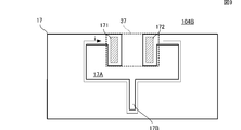
- FIG. 9 is a plan view of an antenna device 104B different from the antenna device shown in FIG.
- a slit 17B connected to the opening 17A is further formed on the conductor surface 17.
- This slit 17B it is possible to radiate the magnetic field also from the slit 17B portion, and the peak position of the magnetic field radiation is moved in the direction in which the slit 17B extends (the directional center of the magnetic field radiation is inclined in the direction in which the slit 17B extends).
- the positions where the slits 17B are formed are not limited to the positions shown in FIG. 9, but may be formed in a direction in which directivity is desired to be expanded. Further, the number of slits to be formed can be changed as appropriate.
- FIG. 10 is a plan view of an antenna device 105 according to the fifth embodiment.
- FIG. 11 is a sectional view taken along line XX in FIG.
- the feed element 37 is mounted at an arbitrary position on the conductor surface 17.
- the terminal conductor pattern 372b, the capacitor formed by the terminal conductor patterns 373a and 373b, the second coil L22, the terminal conductor pattern 372a, and the conductor An opening is formed along the path of the surface 17. This opening acts as a radiation part.
- an opening as indicated by an arrow in the drawing is formed between the second coil and the conductor surface of the power feeding element. And this opening acts as a radiating portion.
- emission means is realizable only by mounting a feed element on a conductor surface. Therefore, the antenna device 105 has directivity in the direction of arrow A in FIG.
- FIG. 12A is a top view of the antenna device 106 according to the sixth embodiment
- FIG. 12B is a cross-sectional view.
- the antenna device 106 includes a conductor surface 18 in which an opening 18A is formed.
- a first mounting portion 181 and a second mounting portion 182 that are isolated from the conductor surface 18 are formed in the opening 18 ⁇ / b> A of the conductor surface 18.
- the first mounting portion 181 is connected to the terminal conductor pattern 372 a of the power feeding element 37.
- a terminal conductor pattern 372 b of the power feeding element 37 is connected to the second mounting portion 182.
- the antenna device 106 includes a conductor surface 19 disposed to face the conductor surface 18.
- the conductor surface 19 is a part of a metal housing, for example.
- the conductor surface 19 is connected to the first mounting portion 181 and the second mounting portion 182 through the first connection portion 21 and the second connection portion 22.
- the 1st connection part 21 and the 2nd connection part 22 are spring connectors etc., for example.
- the terminal conductor pattern 372b When viewed in cross-section with this configuration, as shown by the arrow in FIG. 12B, the terminal conductor pattern 372b, the capacitor formed by the flat conductor patterns 373a and 373b, the second coil L22, and the terminal conductor pattern 372a.
- An opening is formed in the path of the first connection portion 21, the conductor surface 19, and the second connection portion 22. This opening acts as a radiation part. Therefore, the antenna device 106 points in the direction of arrow A in FIG.
- FIG. 13 is a plan view of an antenna device 107 according to the seventh embodiment.
- the power feeding element 36 shown in FIG. 2 is used.
- an opening 20A is formed in the conductor surface 20, and a first mounting portion 201 and a second mounting portion 202 are formed in the opening 20A.
- a terminal electrode P3 connected to the first end of the second coil L22 of the power feeding element 36 is connected to the first mounting part 201, and a second of the second coil L22 of the power feeding element 36 is connected to the second mounting part 202.
- a terminal electrode P1 to which the ends are connected is connected.
- a third mounting portion 203 and a fourth mounting portion 204 are further formed separately from each other.
- the third mounting portion 203 is mounted with a first connection portion 21 that is connected to a conductor surface (not shown) (conductor surface 19 in FIG. 12), and the fourth mounting portion 204 has a conductor surface (not shown) (not shown). 12 conductor surfaces 19) are connected.
- An inductor L3 is connected between the first mounting unit 201 and the third mounting unit 203.
- a capacitor C3 is connected between the second mounting unit 202 and the fourth mounting unit 204.
- the opening 20A is formed with power supply circuit side mounting portions 611 and 612 to which the terminal electrode P4 connected to the first end of the first coil L21 and the terminal electrode P2 connected to the second end are respectively connected.
- the RFIC 60 is connected to the power feeding circuit side mounting portions 611 and 612.
- the power feeding element 36 does not contain a capacitor
- the actual capacitor C3 By mounting the actual capacitor C3 outside the power feeding element 36, it acts as a radiating portion as in the case of FIG. An opening can be formed.
- the resonance frequency By mounting the capacitor C3 outside the feed element 36, the resonance frequency can be adjusted.
- the inductance component of the resonance circuit can be determined by the inductance of the inductor L3, it has an appropriate inductance depending on the size and shape of the conductor surface with which the first connection portion 21 and the second connection portion 22 abut.
- An inductor L3 can be defined.
- a capacitor may be mounted instead of the inductor L3.
- the first coil L21 and the second coil L22 are formed so that the coil winding axis is in a direction orthogonal to the stacking direction.
- a formation aspect is not limited to this.
- the first coil L21 and the second coil L22 may be formed with the coil winding axis aligned with the stacking direction of the insulator layers.
- the second coil L22 may be formed inside the coil opening of the first coil L21.
- FIG. 2 and the like an example in which the first coil L21 and the second coil L22 are alternately wound is shown.
- the second coil L22 is inserted into the second coil L22 so as to sandwich the first coil L21.
- the structure wound around the outside of one coil L21 may be sufficient.
- the first coil L21 and the second coil L22 are formed with the same winding axis and coil opening, and the first coil L21 wound a plurality of times is wound a plurality of times.
- Two coils L22 may be arranged, and the first coil L21 wound a plurality of times may be arranged, and the second coil L22 wound a plurality of times may be arranged.
- FIG. 14 is a plan view showing the structure inside the housing of the communication terminal apparatus according to the eighth embodiment.
- 15A is a cross-sectional view in the short side direction of the communication terminal device shown in FIG. 14, and
- FIG. 15B is a cross-sectional view in the long side direction of the communication terminal device.
- the upper housing side is shown facing downward.
- circuit boards 61, 71, 81, a camera module 76, a battery pack 83, and the like are housed.
- An RFIC 60 (not shown) provided with a communication circuit, a power feeding element 36, and the like are mounted on the circuit board 61.
- a UHF band antenna 72 and the like are mounted on the circuit board 71.
- a UHF band antenna 82 and the like are mounted on the circuit board 81.
- Each of the circuit boards 61, 71, 81 is connected via a cable.
- the ground conductor formed on the circuit board 61 acts as a conductor surface.
- the ground conductor of the circuit board 61 has a notch formed in part, and a mounting part for mounting the power feeding element 37 is formed in the part.
- the power feeding element 37 is the same as that described with reference to FIG.
- a mounting portion 61A provided with the second connection portion 22 is provided in the notched portion.
- the mounting portion 61A is connected to the ground conductor of the circuit board 61 via the capacitor C3, the second coil L22 of the power feeding element 37, and the inductor L3.
- the upper casing 91 is a metal casing.
- the ground conductor of the circuit board 61 is connected to the upper housing 91 via the fourth connection portion 24.
- the lower casing 92 is made of resin, and the conductor surface 12 made of a metal film is formed on the inner surface thereof.
- the second connection portion 22 provided in the mounting portion 61A is connected to the conductor surface 12. Further, the metal film of the upper housing 91 and the conductor surface 12 are electrically connected by the first connection portion 21.
- the second coil L22 of the feed element ⁇ the capacitor C3 ⁇ the mounting portion 61A ⁇ the second connection portion 22 ⁇ the conductor surface 12 ⁇ the first connection portion 21 ⁇ the upper housing.
- the current i flows through a path of 91 ⁇ the fourth connection portion 24 ⁇ the ground conductor of the circuit board 61 ⁇ the inductor L3 ⁇ the second coil L22.
- This current path is an opening that acts as a radiation portion.
- the magnetic flux ⁇ 2 enters and exits the opening.
- An element such as a capacitor or an inductor may be mounted on the path of the opening that acts as the radiating portion as appropriate in order to match a desired resonance frequency.
- FIGS. 16A and 16B are diagrams illustrating an example of a joint structure between an upper housing and a lower housing.
- the upper housing 91 is a metal housing.
- a configuration may be adopted in which a part of the metal film serving as the conductor surface 12 is refracted and fixed to the upper housing 91 with screws 93. Thereby, the conductor surface 12 and the upper housing 91 are electrically connected.
- a fitting portion 121 may be formed on the metal film that becomes the conductor surface 12, and the fitting portion 121 may be pressed and fixed to the housing 91. Thereby, the conductor surface 12 and the upper housing 91 are electrically connected.
- the opening serving as the radiating portion is formed in the short side direction of the communication terminal device.
- the opening may be formed in the long side direction or in the diagonal direction of the housing. Good.
- FIG. 17 is a plan view showing the structure inside the housing of the communication terminal device according to the ninth embodiment.
- the metal film that becomes the conductor surface 12 is not formed on the lower housing 92.
- the upper casing 91 is provided with a battery pack 83 and a circuit board 73, and UHF band antennas 72 and 82 and a camera module 76 are mounted on the circuit board 73.
- a slit 73S is formed in a portion of the circuit board 73 where the ground pattern is not formed.
- an opening 73A is formed in the vicinity of the slit 73S.
- the feeding circuit side mounting portions 611 and 612 are formed in the opening 73A, and the RFIC 60, the capacitor C4, and the like are mounted. .
- a capacitor C3 is provided between the slit 73S and the opening 73A.
- the power feeding circuit side mounting portion is formed between the slit 73S and the opening 73A, and the power feeding element 36 is mounted on the mounting portion.
- One of the conductor films according to the present invention is not limited to a ground conductor or a battery pack formed on a circuit board.
- one side is not restricted to the metal part of a housing
- a shield case, a shield plate, an LCD panel, or the like may be used as the first conductor surface or the second conductor surface.
Landscapes
- Engineering & Computer Science (AREA)
- Physics & Mathematics (AREA)
- Health & Medical Sciences (AREA)
- Toxicology (AREA)
- Theoretical Computer Science (AREA)
- General Physics & Mathematics (AREA)
- Microelectronics & Electronic Packaging (AREA)
- Artificial Intelligence (AREA)
- General Health & Medical Sciences (AREA)
- Computer Vision & Pattern Recognition (AREA)
- Electromagnetism (AREA)
- Power Engineering (AREA)
- Computer Networks & Wireless Communication (AREA)
- Computer Hardware Design (AREA)
- Multimedia (AREA)
- Support Of Aerials (AREA)
- Near-Field Transmission Systems (AREA)
- Waveguide Aerials (AREA)
- Charge And Discharge Circuits For Batteries Or The Like (AREA)
- Details Of Aerials (AREA)
- Aerials With Secondary Devices (AREA)
Description
導体部材と、前記導体部材に対して高周波信号を給電する給電素子とを備え、
前記給電素子は、給電回路に接続される第1コイルと、前記第1コイルと磁界結合する第2コイルと、前記第2コイルを前記導体部材に接続する2つの端子電極と、を絶縁体素体に一体的に備えて構成されたことを特徴とする。
アンテナ装置を構成するために導体部材とともに用いられ、
絶縁体素体を備え、給電回路に接続される第1コイルと、前記第1コイルと磁界結合する第2コイルと、前記第2コイルを前記導体部材に接続する2つの端子電極と、が前記絶縁体素体に一体的に形成されたことを特徴とする。
アンテナ装置と、このアンテナ装置に接続された給電回路とを備え、
前記アンテナ装置は、
導体部材と、前記導体部材に対して高周波信号を給電する給電素子とを備え、
前記給電素子は、給電回路に接続される第1コイルと、前記第1コイルと磁界結合する第2コイルと、前記第2コイルを前記導体部材に接続する2つの端子電極と、を絶縁体素体に一体的に備えて構成されたことを特徴とする。
図1は第1の実施形態に係るアンテナ装置101の平面図である。図2は、第1の実施形態に係る給電素子36の分解斜視図である。図3は、第1の実施形態に係るアンテナ装置101の磁界の放射を説明するための図である。図1および図3では、給電素子36については、外形を示し、内部に有する第1のコイルL21と第2のコイルL22とを回路記号で示している。
図5は、第2の実施形態に係るアンテナ装置102の平面図である。このアンテナ装置102では、導体面15には、開放部を有し、閉じられていない二つの開口15A,15Bが形成されている。開口15A,15Bの間には、給電素子36の第2のコイルL22の第1端が接続される第1実装部151と、第2端が接続される第2実装部152とが形成されている。第1実装部151は、直接または間接(例えばキャパシタを介して)に導体面15と接続している。第1実装部151は導体面15と一体的なものであってもよいし、導体面15とは別部材で構成され、この別部材が導体面15に接続されていてもよい。
図6は、第3の実施形態に係るアンテナ装置103の平面図である。このアンテナ装置103では、導体面16には、図5と同様、二つの開口16A,16Bが形成されている。開口16A,16Bの間には、給電素子36の第2のコイルL22の第1端が接続される第1実装部161と、第2端が接続される第2実装部162とが形成されている。第1実装部161は、直接または間接に導体面16に接続されている。第2実装部162と導体面16との間にはキャパシタC3が接続されている。
第1~第3の実施形態では、共振回路を構成するために、実部品のキャパシタC3を導体面に実装しているのに対し、第4の実装形態では、給電素子がキャパシタを内蔵している。
図10は、第5の実施形態に係るアンテナ装置105の平面図である。図11は、図10のX-X線における断面図である。この例のアンテナ装置105では、導体面17には開口が形成されておらず、給電素子37が導体面17の任意の位置に実装されている。この場合、断面視すると、図11の太線矢印で示すように、端子用導体パターン372b、端子用導体パターン373a,373bで形成されるキャパシタ、第2のコイルL22、端子用導体パターン372a、および導体面17の経路で開口が形成される。この開口が放射部として作用する。すなわち、この構成では、給電素子37の長手方向の側面(積層方向に直交する方向)から視た場合に、給電素子の第2のコイルと導体面とで図中矢印のような開口(ループ)が形成され、この開口が放射部として作用する。これにより、給電素子を導体面に実装するだけで放射手段を実現できる。したがって、アンテナ装置105は、図10の矢印A方向に指向性を有する。
第6の実施形態では、図7で示した給電素子37を用いて、二つの導体面で放射部として作用する開口を形成する。図12(A)は、第6の実施形態に係るアンテナ装置106の上面図、図12(B)は断面図である。
図13は、第7の実施形態に係るアンテナ装置107の平面図である。この例では、図2で示した給電素子36を用いている。アンテナ装置107は、導体面20に開口20Aが形成されていて、開口20Aに第1実装部201と第2実装部202とが形成されている。第1実装部201には、給電素子36の第2のコイルL22の第1端がつながる端子電極P3が接続され、第2実装部202には、給電素子36の第2のコイルL22の第2端がつながる端子電極P1が接続される。
図14は、第8の実施形態に係る通信端末装置の筐体内部の構造を示す平面図である。図15(A)は、図14に示す通信端末装置の短辺方向における断面図、図15(B)は、通信端末装置の長辺方向における断面図である。但し、図15(A)(B)においては、上部筐体側を図の下に向けて表している。
図17は、第9の実施形態に係る通信端末装置の筐体内部の構造を示す平面図である。この例では、下部筐体92に導体面12となる金属膜は形成されていない。
L21…第1のコイル
L22…第2のコイル
P1,P2,P3,P4…端子電極
12…導体面
14~20…導体面
14A,18A,20A…開口
15A,15B…開口
16A,16B…開口
17A,17B…スリット
21…第1接続部
22…第2接続部
24…第4接続部
36,37…給電素子
60…RFIC
61,71,81…回路基板
61A…実装部
71,81…回路基板
72,82…UHF帯アンテナ
73…回路基板
73A…開口
73S…スリット
76…カメラモジュール
83…バッテリーパック
91…上部筐体
92…下部筐体
101~107…アンテナ装置
121…嵌合部
141,151,161,171,181,201,…第1実装部
142,152,162,172,182,202…第2実装部
203…第3実装部
204…第4実装部
361a,361b,361c,361d…絶縁体層
361a,361d…非磁性体層
361b,361c…磁性体層
362a,362b…コイル用導体パターン
363a,363b…コイル用導体パターン
371a~371g…絶縁体層
371a,371d~371g…非磁性体層
371b,371c…磁性体層
372a,372b…端子用導体パターン
373a,373b…平板状導体パターン
611,612…給電回路側実装部
Claims (13)
- 導体部材と、前記導体部材に対して高周波信号を給電する給電素子とを備えたアンテナ装置において、
前記給電素子は、給電回路に接続される第1コイルと、前記第1コイルと磁界結合する第2コイルと、前記第2コイルを前記導体部材に接続する2つの端子電極と、を絶縁体素体に一体的に備えて構成されたことを特徴とするアンテナ装置。 - 前記給電素子は、前記2つの端子電極のうち少なくとも一方の端子電極と前記第2コイルの少なくとも一方の端子との間に接続されたキャパシタを備えた、請求項1に記載のアンテナ装置。
- 前記導体部材は基板に形成された導体膜であり、前記基板は、前記給電素子の2つの端子電極のうち少なくとも一方の端子電極が接続される端子と、この端子と前記導体部材との間に接続されたキャパシタとを備える、請求項1に記載のアンテナ装置。
- 前記導体部材、前記キャパシタおよび前記第1コイルにより共振回路が構成されている、請求項2または3に記載のアンテナ装置。
- 前記キャパシタのキャパシタンスおよび前記第1コイルのインダクタンスは、前記共振回路の共振周波数が、通信周波数となるように、または通信周波数に近似するように、定められている、請求項4に記載のアンテナ装置。
- 前記第2のコイルのインダクタンスは、前記2つの端子電極から見た前記導体部材のインダクタンス成分よりも小さい、請求項1~5のいずれかに記載のアンテナ装置。
- 前記導体部材は、端縁から内部へ入り込むスリットまたは開口を備え、前記2つの端子電極は前記スリットまたは開口を跨ぐ位置に配置されている、請求項1~6のいずれかに記載のアンテナ装置。
- 前記給電素子は、前記第1のコイルおよび前記第2のコイルを形成する導体が形成された複数の絶縁体層が積層された積層構造体である、請求項1~7のいずれかに記載のアンテナ装置。
- 前記給電素子は、前記第1のコイルおよび前記第2のコイルを形成する導体が形成された複数の絶縁体層および前記キャパシタを形成する導体が形成された複数の絶縁体層を備える、請求項2に記載のアンテナ装置。
- 前記導体膜は、前記基板に形成された回路のグランド電極またはシールド電極である、請求項3に記載のアンテナ装置。
- 前記給電回路はRFICを有し、前記RFICは前記絶縁体素体に搭載されている、請求項1~10のいずれかに記載のアンテナ装置。
- 導体部材とともにアンテナ装置を構成する給電素子において、
絶縁体素体を備え、給電回路に接続される第1コイルと、前記第1コイルと磁界結合する第2コイルと、前記第2コイルを前記導体部材に接続する2つの端子電極と、が前記絶縁体素体に一体的に形成されたことを特徴とする給電素子。 - アンテナ装置と、このアンテナ装置に接続された給電回路とを備えた通信端末装置において、
前記アンテナ装置は、
導体部材と、前記導体部材に対して高周波信号を給電する給電素子とを備え、
前記給電素子は、給電回路に接続される第1コイルと、前記第1コイルと磁界結合する第2コイルと、前記第2コイルを前記導体部材に接続する2つの端子電極と、を絶縁体素体に一体的に備えて構成されたことを特徴とする通信端末装置。
Priority Applications (5)
| Application Number | Priority Date | Filing Date | Title |
|---|---|---|---|
| GB1422836.5A GB2519247B (en) | 2012-06-28 | 2013-06-28 | Antenna device, feed element, and communication terminal device |
| JP2013552787A JP5655959B2 (ja) | 2012-06-28 | 2013-06-28 | アンテナ装置、給電素子および通信端末装置 |
| CN201380002129.XA CN103650242B (zh) | 2012-06-28 | 2013-06-28 | 天线装置、供电元件及通信终端装置 |
| US14/221,437 US9531072B2 (en) | 2012-06-28 | 2014-03-21 | Antenna device, feed element, and communication terminal device |
| US15/272,684 US9947995B2 (en) | 2012-06-28 | 2016-09-22 | Antenna device, feed element, and communication terminal device |
Applications Claiming Priority (6)
| Application Number | Priority Date | Filing Date | Title |
|---|---|---|---|
| JP2012-144968 | 2012-06-28 | ||
| JP2012144968 | 2012-06-28 | ||
| JP2012202755 | 2012-09-14 | ||
| JP2012-202755 | 2012-09-14 | ||
| JP2012-226975 | 2012-10-12 | ||
| JP2012226975 | 2012-10-12 |
Related Child Applications (1)
| Application Number | Title | Priority Date | Filing Date |
|---|---|---|---|
| US14/221,437 Continuation US9531072B2 (en) | 2012-06-28 | 2014-03-21 | Antenna device, feed element, and communication terminal device |
Publications (1)
| Publication Number | Publication Date |
|---|---|
| WO2014003164A1 true WO2014003164A1 (ja) | 2014-01-03 |
Family
ID=49783298
Family Applications (1)
| Application Number | Title | Priority Date | Filing Date |
|---|---|---|---|
| PCT/JP2013/067805 Ceased WO2014003164A1 (ja) | 2012-06-28 | 2013-06-28 | アンテナ装置、給電素子および通信端末装置 |
Country Status (5)
| Country | Link |
|---|---|
| US (2) | US9531072B2 (ja) |
| JP (4) | JP5655959B2 (ja) |
| CN (6) | CN105977643B (ja) |
| GB (3) | GB2519247B (ja) |
| WO (1) | WO2014003164A1 (ja) |
Cited By (6)
| Publication number | Priority date | Publication date | Assignee | Title |
|---|---|---|---|---|
| CN104933460A (zh) * | 2014-03-20 | 2015-09-23 | 中兴通讯股份有限公司 | 一种rfid标签和动态启动rfid标签的装置 |
| JP5825457B1 (ja) * | 2014-02-14 | 2015-12-02 | 株式会社村田製作所 | アンテナ装置および無線通信装置 |
| US9531072B2 (en) | 2012-06-28 | 2016-12-27 | Murata Manufacturing Co., Ltd. | Antenna device, feed element, and communication terminal device |
| JPWO2015166834A1 (ja) * | 2014-04-30 | 2017-04-20 | 株式会社村田製作所 | アンテナ装置および電子機器 |
| WO2018056422A1 (ja) * | 2016-09-26 | 2018-03-29 | 株式会社村田製作所 | アンテナ装置および電子機器 |
| WO2018056101A1 (ja) * | 2016-09-26 | 2018-03-29 | 株式会社村田製作所 | アンテナ装置および電子機器 |
Families Citing this family (14)
| Publication number | Priority date | Publication date | Assignee | Title |
|---|---|---|---|---|
| EP0505555B1 (en) | 1990-10-24 | 1998-06-17 | Sony Music Entertainment Inc. | Method and apparatus for high speed duplication of audio or digital signals |
| CN102668241B (zh) * | 2010-03-24 | 2015-01-28 | 株式会社村田制作所 | Rfid系统 |
| US8988305B1 (en) * | 2013-10-22 | 2015-03-24 | Eray Innovation | Portable wireless phone device |
| CN106134000B (zh) * | 2014-04-28 | 2019-04-02 | 株式会社村田制作所 | 无线ic器件、夹状rfid标签以及附带rfid标签的物品 |
| FR3030908B1 (fr) * | 2014-12-18 | 2016-12-09 | Stmicroelectronics Rousset | Antenne pour dispositif electronique |
| JP6589403B2 (ja) * | 2015-06-15 | 2019-10-16 | Tdk株式会社 | アンテナ装置及びこれに用いるコイル部品 |
| CN208189791U (zh) * | 2015-10-16 | 2018-12-04 | 株式会社村田制作所 | 天线电路以及通信装置 |
| CN110120583A (zh) * | 2016-01-14 | 2019-08-13 | 株式会社村田制作所 | 天线装置以及电子设备 |
| US10522912B2 (en) * | 2016-05-12 | 2019-12-31 | Tdk Corporation | Antenna device and mobile wireless device provided with the same |
| KR101824998B1 (ko) | 2016-07-13 | 2018-02-02 | 엘지전자 주식회사 | 이동 단말기 |
| WO2018123345A1 (ja) * | 2016-12-27 | 2018-07-05 | 株式会社村田製作所 | アンテナ装置 |
| CN109565114B (zh) | 2017-07-06 | 2020-08-04 | 株式会社村田制作所 | 电子设备 |
| CN110009886A (zh) * | 2018-01-04 | 2019-07-12 | 法雷奥汽车内部控制(深圳)有限公司 | 抗干扰器件和包括所述抗干扰器件的遥控装置 |
| JP7196007B2 (ja) * | 2019-04-17 | 2022-12-26 | 日本航空電子工業株式会社 | アンテナ |
Citations (3)
| Publication number | Priority date | Publication date | Assignee | Title |
|---|---|---|---|---|
| WO2010104179A1 (ja) * | 2009-03-13 | 2010-09-16 | 株式会社村田製作所 | 信号処理回路及びアンテナ装置 |
| JP2012019527A (ja) * | 2006-04-26 | 2012-01-26 | Murata Mfg Co Ltd | 携帯端末機器 |
| JP2012085250A (ja) * | 2010-08-11 | 2012-04-26 | Murata Mfg Co Ltd | 周波数安定化回路、アンテナ装置及び通信端末機器 |
Family Cites Families (53)
| Publication number | Priority date | Publication date | Assignee | Title |
|---|---|---|---|---|
| US3736591A (en) * | 1970-10-30 | 1973-05-29 | Motorola Inc | Receiving antenna for miniature radio receiver |
| JPH01246904A (ja) * | 1988-03-28 | 1989-10-02 | Kokusai Electric Co Ltd | 小形アンテナ |
| NL9100176A (nl) * | 1991-02-01 | 1992-03-02 | Nedap Nv | Antenne met transformator voor contactloze informatieoverdracht vanuit integrated circuit-kaart. |
| DE19703029A1 (de) * | 1997-01-28 | 1998-07-30 | Amatech Gmbh & Co Kg | Übertragungsmodul für eine Transpondervorrichtung sowie Transpondervorrichtung und Verfahren zum Betrieb einer Transpondervorrichtung |
| WO1999026195A1 (en) * | 1997-11-14 | 1999-05-27 | Toppan Printing Co., Ltd. | Composite ic module and composite ic card |
| CA2312153A1 (en) * | 1997-12-09 | 1999-06-17 | The Goodyear Tire & Rubber Company | Antenna for radio transponder |
| EP0977145A3 (en) * | 1998-07-28 | 2002-11-06 | Kabushiki Kaisha Toshiba | Radio IC card |
| GB2348321A (en) * | 1999-03-23 | 2000-09-27 | Mitel Semiconductor Ltd | A laminated transformer and a method of its manufacture |
| JP2001266100A (ja) * | 2000-03-22 | 2001-09-28 | Dainippon Printing Co Ltd | 非接触式データキャリアおよび非接触データキャリア付ケース |
| FR2812482B1 (fr) * | 2000-07-28 | 2003-01-24 | Inside Technologies | Dispositif electronique portable comprenant plusieurs circuits integres sans contact |
| JP4016322B2 (ja) * | 2002-05-10 | 2007-12-05 | 株式会社エフ・イー・シー | Icカード |
| US7699231B2 (en) | 2003-08-13 | 2010-04-20 | Murata Manufacturing Co., Ltd. | Reader/writer and mobile communication apparatus |
| JP3982476B2 (ja) | 2003-10-01 | 2007-09-26 | ソニー株式会社 | 通信システム |
| WO2005043566A1 (ja) * | 2003-11-04 | 2005-05-12 | Tamura Corporation | 積層型磁性部品及びその製造方法並びに積層型磁性部品用積層体の製造方法 |
| US7551058B1 (en) * | 2003-12-10 | 2009-06-23 | Advanced Design Consulting Usa, Inc. | Sensor for monitoring environmental parameters in concrete |
| US20060012482A1 (en) * | 2004-07-16 | 2006-01-19 | Peter Zalud | Radio frequency identification tag having an inductively coupled antenna |
| ITMO20040193A1 (it) * | 2004-07-23 | 2004-10-23 | Angelo Grandi Cucine Spa | Sistema e sonda per la rivealzione di un parametro |
| US20080211635A1 (en) | 2005-04-08 | 2008-09-04 | Nxp B.V. | Rfid Reader With An Antenna And Method For Operating The Same |
| JP2007143063A (ja) * | 2005-11-22 | 2007-06-07 | Alps Electric Co Ltd | アンテナ装置 |
| JP2007165968A (ja) | 2005-12-09 | 2007-06-28 | Matsushita Electric Ind Co Ltd | アンテナ装置 |
| FI119010B (fi) * | 2006-01-09 | 2008-06-13 | Pulse Finland Oy | RFID-antenni |
| JP4780460B2 (ja) * | 2006-03-23 | 2011-09-28 | 日立金属株式会社 | チップアンテナ、アンテナ装置および通信機器 |
| JP2007288742A (ja) * | 2006-04-20 | 2007-11-01 | Alps Electric Co Ltd | 小型広帯域アンテナ装置 |
| US9064198B2 (en) | 2006-04-26 | 2015-06-23 | Murata Manufacturing Co., Ltd. | Electromagnetic-coupling-module-attached article |
| BRPI0702919B1 (pt) | 2006-04-26 | 2019-05-07 | Murata Manufacturing Co., Ltd | Artigo com um módulo de acoplamento eletromagnético |
| US8026818B2 (en) * | 2006-12-20 | 2011-09-27 | Checkpoint Systems, Inc. | EAS and UHF combination tag |
| CN101239604A (zh) * | 2007-02-09 | 2008-08-13 | 纽奥奇有限公司 | 电子车牌 |
| CN104540317B (zh) | 2007-07-17 | 2018-11-02 | 株式会社村田制作所 | 印制布线基板 |
| US20090021352A1 (en) * | 2007-07-18 | 2009-01-22 | Murata Manufacturing Co., Ltd. | Radio frequency ic device and electronic apparatus |
| JP2009075687A (ja) * | 2007-09-19 | 2009-04-09 | Hitachi Ltd | Rfidタグ |
| DE102007062051A1 (de) | 2007-12-21 | 2009-06-25 | Siemens Home And Office Communication Devices Gmbh & Co. Kg | Antennenvorrichtung für funkbasierte elektronische Geräte |
| EP2557528A3 (en) * | 2007-12-26 | 2017-01-18 | Murata Manufacturing Co., Ltd. | Antenna device and wireless IC device |
| JP4404166B2 (ja) * | 2008-03-26 | 2010-01-27 | 株式会社村田製作所 | 無線icデバイス |
| JP2009283771A (ja) * | 2008-05-23 | 2009-12-03 | Toshiba Tec Corp | 積層プリント基板 |
| JP5041077B2 (ja) * | 2009-01-16 | 2012-10-03 | 株式会社村田製作所 | 高周波デバイス及び無線icデバイス |
| US20100201578A1 (en) | 2009-02-12 | 2010-08-12 | Harris Corporation | Half-loop chip antenna and associated methods |
| CN201490334U (zh) * | 2009-04-03 | 2010-05-26 | 中兴通讯股份有限公司 | 近场通信天线装置 |
| WO2011001709A1 (ja) * | 2009-07-03 | 2011-01-06 | 株式会社村田製作所 | アンテナおよびアンテナモジュール |
| GB2487491B (en) * | 2009-11-20 | 2014-09-03 | Murata Manufacturing Co | Antenna device and mobile communication terminal |
| US8270914B2 (en) * | 2009-12-03 | 2012-09-18 | Apple Inc. | Bezel gap antennas |
| WO2011090082A1 (ja) * | 2010-01-19 | 2011-07-28 | 株式会社村田製作所 | 高結合度トランス、電子回路および電子機器 |
| EP2388858B1 (en) * | 2010-01-19 | 2016-09-21 | Murata Manufacturing Co., Ltd. | Antenna device and communication terminal apparatus |
| TW201134000A (en) | 2010-03-16 | 2011-10-01 | Chi Mei Comm Systems Inc | Wireless communication device |
| JP4934784B2 (ja) * | 2010-04-12 | 2012-05-16 | 株式会社村田製作所 | アンテナ装置及び通信端末装置 |
| WO2011132701A1 (ja) * | 2010-04-22 | 2011-10-27 | 株式会社村田製作所 | 無線通信システム |
| IT1401521B1 (it) * | 2010-08-11 | 2013-07-26 | St Microelectronics Srl | Sistema di sicurezza per almeno un circuito integrato ic, scheda a circuito integrato in sicurezza e metodo di comunicazione wireless in sicurezza. |
| CN103038939B (zh) * | 2010-09-30 | 2015-11-25 | 株式会社村田制作所 | 无线ic器件 |
| EP2453585A1 (en) * | 2010-11-11 | 2012-05-16 | Nxp B.V. | Near-field communications system |
| JP5590414B2 (ja) | 2010-12-22 | 2014-09-17 | 清水建設株式会社 | 変位制御材の最適剛性設定方法 |
| JP5605251B2 (ja) * | 2011-02-04 | 2014-10-15 | 株式会社村田製作所 | 無線icデバイス |
| JP5263324B2 (ja) | 2011-03-24 | 2013-08-14 | 株式会社デンソー | 空気流量測定装置 |
| JP5678787B2 (ja) | 2011-04-20 | 2015-03-04 | オムロン株式会社 | 押しボタンスイッチ |
| GB2519247B (en) | 2012-06-28 | 2017-11-29 | Murata Manufacturing Co | Antenna device, feed element, and communication terminal device |
-
2013
- 2013-06-28 GB GB1422836.5A patent/GB2519247B/en not_active Expired - Fee Related
- 2013-06-28 GB GB1617842.8A patent/GB2540690B/en not_active Expired - Fee Related
- 2013-06-28 CN CN201610325254.XA patent/CN105977643B/zh active Active
- 2013-06-28 GB GB1701500.9A patent/GB2543985B/en not_active Expired - Fee Related
- 2013-06-28 WO PCT/JP2013/067805 patent/WO2014003164A1/ja not_active Ceased
- 2013-06-28 CN CN201610325280.2A patent/CN105975889B/zh active Active
- 2013-06-28 CN CN201610325271.3A patent/CN106058474B/zh active Active
- 2013-06-28 JP JP2013552787A patent/JP5655959B2/ja not_active Expired - Fee Related
- 2013-06-28 CN CN201610324288.7A patent/CN105977642B/zh active Active
- 2013-06-28 CN CN201380002129.XA patent/CN103650242B/zh active Active
- 2013-06-28 CN CN201510133141.5A patent/CN104733862B/zh active Active
-
2014
- 2014-03-21 US US14/221,437 patent/US9531072B2/en active Active
- 2014-11-21 JP JP2014236817A patent/JP5846284B2/ja not_active Expired - Fee Related
-
2015
- 2015-11-24 JP JP2015228552A patent/JP6090412B2/ja not_active Expired - Fee Related
-
2016
- 2016-09-22 US US15/272,684 patent/US9947995B2/en active Active
-
2017
- 2017-02-07 JP JP2017020115A patent/JP6260729B2/ja not_active Expired - Fee Related
Patent Citations (3)
| Publication number | Priority date | Publication date | Assignee | Title |
|---|---|---|---|---|
| JP2012019527A (ja) * | 2006-04-26 | 2012-01-26 | Murata Mfg Co Ltd | 携帯端末機器 |
| WO2010104179A1 (ja) * | 2009-03-13 | 2010-09-16 | 株式会社村田製作所 | 信号処理回路及びアンテナ装置 |
| JP2012085250A (ja) * | 2010-08-11 | 2012-04-26 | Murata Mfg Co Ltd | 周波数安定化回路、アンテナ装置及び通信端末機器 |
Cited By (12)
| Publication number | Priority date | Publication date | Assignee | Title |
|---|---|---|---|---|
| US9531072B2 (en) | 2012-06-28 | 2016-12-27 | Murata Manufacturing Co., Ltd. | Antenna device, feed element, and communication terminal device |
| JP5825457B1 (ja) * | 2014-02-14 | 2015-12-02 | 株式会社村田製作所 | アンテナ装置および無線通信装置 |
| JP2016067006A (ja) * | 2014-02-14 | 2016-04-28 | 株式会社村田製作所 | アンテナ装置および無線通信装置 |
| US9846834B2 (en) | 2014-02-14 | 2017-12-19 | Murata Manufacturing Co., Ltd. | Antenna device and wireless communication device |
| CN104933460A (zh) * | 2014-03-20 | 2015-09-23 | 中兴通讯股份有限公司 | 一种rfid标签和动态启动rfid标签的装置 |
| JPWO2015166834A1 (ja) * | 2014-04-30 | 2017-04-20 | 株式会社村田製作所 | アンテナ装置および電子機器 |
| WO2018056422A1 (ja) * | 2016-09-26 | 2018-03-29 | 株式会社村田製作所 | アンテナ装置および電子機器 |
| WO2018056101A1 (ja) * | 2016-09-26 | 2018-03-29 | 株式会社村田製作所 | アンテナ装置および電子機器 |
| JP6369666B1 (ja) * | 2016-09-26 | 2018-08-08 | 株式会社村田製作所 | アンテナ装置および電子機器 |
| JP6376317B1 (ja) * | 2016-09-26 | 2018-08-22 | 株式会社村田製作所 | アンテナ装置および電子機器 |
| US10505267B2 (en) | 2016-09-26 | 2019-12-10 | Murata Manufacturing Co., Ltd. | Antenna device and electronic apparatus |
| US10530057B2 (en) | 2016-09-26 | 2020-01-07 | Murata Manufacturing, Co., Ltd. | Antenna device and electronic appliance |
Also Published As
| Publication number | Publication date |
|---|---|
| CN105977642A (zh) | 2016-09-28 |
| GB2519247A (en) | 2015-04-15 |
| GB2543985A (en) | 2017-05-03 |
| GB2540690A (en) | 2017-01-25 |
| CN105977642B (zh) | 2019-03-05 |
| CN104733862A (zh) | 2015-06-24 |
| GB2543985B (en) | 2017-10-11 |
| US9947995B2 (en) | 2018-04-17 |
| JP6260729B2 (ja) | 2018-01-17 |
| US20170012350A1 (en) | 2017-01-12 |
| CN106058474A (zh) | 2016-10-26 |
| GB201701500D0 (en) | 2017-03-15 |
| GB2540690B (en) | 2017-09-27 |
| US9531072B2 (en) | 2016-12-27 |
| CN103650242A (zh) | 2014-03-19 |
| CN105977643B (zh) | 2019-11-26 |
| JPWO2014003164A1 (ja) | 2016-06-02 |
| CN104733862B (zh) | 2018-03-02 |
| GB2519247B (en) | 2017-11-29 |
| CN105975889A (zh) | 2016-09-28 |
| CN103650242B (zh) | 2016-07-06 |
| JP2017112633A (ja) | 2017-06-22 |
| US20140203992A1 (en) | 2014-07-24 |
| GB2519247A9 (en) | 2016-11-16 |
| JP2015057921A (ja) | 2015-03-26 |
| GB201617842D0 (en) | 2016-12-07 |
| JP5846284B2 (ja) | 2016-01-20 |
| JP5655959B2 (ja) | 2015-01-21 |
| JP2016040959A (ja) | 2016-03-24 |
| CN105977643A (zh) | 2016-09-28 |
| CN106058474B (zh) | 2020-02-28 |
| JP6090412B2 (ja) | 2017-03-08 |
| CN105975889B (zh) | 2020-01-03 |
Similar Documents
| Publication | Publication Date | Title |
|---|---|---|
| JP6260729B2 (ja) | 給電素子 | |
| JP6256600B2 (ja) | アンテナ装置および電子機器 | |
| US9997834B1 (en) | Antenna device and communication terminal apparatus | |
| US9865924B2 (en) | Antenna device and communication terminal apparatus | |
| US9905926B2 (en) | Antenna device and wireless communication apparatus | |
| JP5578291B2 (ja) | アンテナ装置及び通信端末機器 | |
| CN103620868B (zh) | 天线装置及通信终端装置 | |
| US8638268B2 (en) | Coil antenna and antenna structure | |
| JP2015006010A (ja) | アンテナ装置および通信端末機器 | |
| JP6172407B2 (ja) | アンテナ装置、カード型情報媒体および通信端末装置 | |
| JP2021048530A (ja) | コイルアンテナ、アンテナ装置及び電子機器 |
Legal Events
| Date | Code | Title | Description |
|---|---|---|---|
| ENP | Entry into the national phase |
Ref document number: 2013552787 Country of ref document: JP Kind code of ref document: A |
|
| 121 | Ep: the epo has been informed by wipo that ep was designated in this application |
Ref document number: 13810236 Country of ref document: EP Kind code of ref document: A1 |
|
| ENP | Entry into the national phase |
Ref document number: 1422836 Country of ref document: GB Kind code of ref document: A Free format text: PCT FILING DATE = 20130628 |
|
| WWE | Wipo information: entry into national phase |
Ref document number: 1422836.5 Country of ref document: GB |
|
| NENP | Non-entry into the national phase |
Ref country code: DE |
|
| 122 | Ep: pct application non-entry in european phase |
Ref document number: 13810236 Country of ref document: EP Kind code of ref document: A1 |