WO2014002663A1 - インターポーザ、プリント基板及び半導体装置 - Google Patents
インターポーザ、プリント基板及び半導体装置 Download PDFInfo
- Publication number
- WO2014002663A1 WO2014002663A1 PCT/JP2013/064570 JP2013064570W WO2014002663A1 WO 2014002663 A1 WO2014002663 A1 WO 2014002663A1 JP 2013064570 W JP2013064570 W JP 2013064570W WO 2014002663 A1 WO2014002663 A1 WO 2014002663A1
- Authority
- WO
- WIPO (PCT)
- Prior art keywords
- interposer
- terminal
- capacitor
- power supply
- lsis
- Prior art date
- Legal status (The legal status is an assumption and is not a legal conclusion. Google has not performed a legal analysis and makes no representation as to the accuracy of the status listed.)
- Ceased
Links
Images




Classifications
-
- H—ELECTRICITY
- H10—SEMICONDUCTOR DEVICES; ELECTRIC SOLID-STATE DEVICES NOT OTHERWISE PROVIDED FOR
- H10W—GENERIC PACKAGES, INTERCONNECTIONS, CONNECTORS OR OTHER CONSTRUCTIONAL DETAILS OF DEVICES COVERED BY CLASS H10
- H10W72/00—Interconnections or connectors in packages
-
- H—ELECTRICITY
- H05—ELECTRIC TECHNIQUES NOT OTHERWISE PROVIDED FOR
- H05K—PRINTED CIRCUITS; CASINGS OR CONSTRUCTIONAL DETAILS OF ELECTRIC APPARATUS; MANUFACTURE OF ASSEMBLAGES OF ELECTRICAL COMPONENTS
- H05K1/00—Printed circuits
- H05K1/02—Details
- H05K1/0213—Electrical arrangements not otherwise provided for
- H05K1/0216—Reduction of cross-talk, noise or electromagnetic interference
- H05K1/023—Reduction of cross-talk, noise or electromagnetic interference using auxiliary mounted passive components or auxiliary substances
- H05K1/0231—Capacitors or dielectric substances
-
- H—ELECTRICITY
- H05—ELECTRIC TECHNIQUES NOT OTHERWISE PROVIDED FOR
- H05K—PRINTED CIRCUITS; CASINGS OR CONSTRUCTIONAL DETAILS OF ELECTRIC APPARATUS; MANUFACTURE OF ASSEMBLAGES OF ELECTRICAL COMPONENTS
- H05K1/00—Printed circuits
- H05K1/02—Details
- H05K1/0213—Electrical arrangements not otherwise provided for
- H05K1/0216—Reduction of cross-talk, noise or electromagnetic interference
- H05K1/023—Reduction of cross-talk, noise or electromagnetic interference using auxiliary mounted passive components or auxiliary substances
- H05K1/0233—Filters, inductors or a magnetic substance
-
- H—ELECTRICITY
- H05—ELECTRIC TECHNIQUES NOT OTHERWISE PROVIDED FOR
- H05K—PRINTED CIRCUITS; CASINGS OR CONSTRUCTIONAL DETAILS OF ELECTRIC APPARATUS; MANUFACTURE OF ASSEMBLAGES OF ELECTRICAL COMPONENTS
- H05K1/00—Printed circuits
- H05K1/02—Details
- H05K1/0213—Electrical arrangements not otherwise provided for
- H05K1/0216—Reduction of cross-talk, noise or electromagnetic interference
- H05K1/0236—Electromagnetic band-gap structures
-
- H—ELECTRICITY
- H10—SEMICONDUCTOR DEVICES; ELECTRIC SOLID-STATE DEVICES NOT OTHERWISE PROVIDED FOR
- H10W—GENERIC PACKAGES, INTERCONNECTIONS, CONNECTORS OR OTHER CONSTRUCTIONAL DETAILS OF DEVICES COVERED BY CLASS H10
- H10W70/00—Package substrates; Interposers; Redistribution layers [RDL]
- H10W70/60—Insulating or insulated package substrates; Interposers; Redistribution layers
- H10W70/611—Insulating or insulated package substrates; Interposers; Redistribution layers for connecting multiple chips together
-
- H—ELECTRICITY
- H10—SEMICONDUCTOR DEVICES; ELECTRIC SOLID-STATE DEVICES NOT OTHERWISE PROVIDED FOR
- H10W—GENERIC PACKAGES, INTERCONNECTIONS, CONNECTORS OR OTHER CONSTRUCTIONAL DETAILS OF DEVICES COVERED BY CLASS H10
- H10W70/00—Package substrates; Interposers; Redistribution layers [RDL]
- H10W70/60—Insulating or insulated package substrates; Interposers; Redistribution layers
- H10W70/67—Insulating or insulated package substrates; Interposers; Redistribution layers characterised by their insulating layers or insulating parts
- H10W70/68—Shapes or dispositions thereof
- H10W70/685—Shapes or dispositions thereof comprising multiple insulating layers
-
- H—ELECTRICITY
- H10—SEMICONDUCTOR DEVICES; ELECTRIC SOLID-STATE DEVICES NOT OTHERWISE PROVIDED FOR
- H10W—GENERIC PACKAGES, INTERCONNECTIONS, CONNECTORS OR OTHER CONSTRUCTIONAL DETAILS OF DEVICES COVERED BY CLASS H10
- H10W90/00—Package configurations
-
- H—ELECTRICITY
- H05—ELECTRIC TECHNIQUES NOT OTHERWISE PROVIDED FOR
- H05K—PRINTED CIRCUITS; CASINGS OR CONSTRUCTIONAL DETAILS OF ELECTRIC APPARATUS; MANUFACTURE OF ASSEMBLAGES OF ELECTRICAL COMPONENTS
- H05K1/00—Printed circuits
- H05K1/02—Details
- H05K1/09—Use of materials for the conductive, e.g. metallic pattern
- H05K1/092—Dispersed materials, e.g. conductive pastes or inks
- H05K1/095—Dispersed materials, e.g. conductive pastes or inks for polymer thick films, i.e. having a permanent organic polymeric binder
-
- H—ELECTRICITY
- H05—ELECTRIC TECHNIQUES NOT OTHERWISE PROVIDED FOR
- H05K—PRINTED CIRCUITS; CASINGS OR CONSTRUCTIONAL DETAILS OF ELECTRIC APPARATUS; MANUFACTURE OF ASSEMBLAGES OF ELECTRICAL COMPONENTS
- H05K1/00—Printed circuits
- H05K1/18—Printed circuits structurally associated with non-printed electric components
- H05K1/182—Printed circuits structurally associated with non-printed electric components associated with components mounted in printed circuit boards [PCB], e.g. insert-mounted components [IMC]
- H05K1/185—Printed circuits structurally associated with non-printed electric components associated with components mounted in printed circuit boards [PCB], e.g. insert-mounted components [IMC] associated with components encapsulated in the insulating substrate of the PCBs; associated with components incorporated in internal layers of multilayer circuit boards
-
- H—ELECTRICITY
- H05—ELECTRIC TECHNIQUES NOT OTHERWISE PROVIDED FOR
- H05K—PRINTED CIRCUITS; CASINGS OR CONSTRUCTIONAL DETAILS OF ELECTRIC APPARATUS; MANUFACTURE OF ASSEMBLAGES OF ELECTRICAL COMPONENTS
- H05K2201/00—Indexing scheme relating to printed circuits covered by H05K1/00
- H05K2201/10—Details of components or other objects attached to or integrated in a printed circuit board
- H05K2201/10227—Other objects, e.g. metallic pieces
- H05K2201/10378—Interposers
-
- H—ELECTRICITY
- H10—SEMICONDUCTOR DEVICES; ELECTRIC SOLID-STATE DEVICES NOT OTHERWISE PROVIDED FOR
- H10W—GENERIC PACKAGES, INTERCONNECTIONS, CONNECTORS OR OTHER CONSTRUCTIONAL DETAILS OF DEVICES COVERED BY CLASS H10
- H10W44/00—Electrical arrangements for controlling or matching impedance
- H10W44/20—Electrical arrangements for controlling or matching impedance at high-frequency [HF] or radio frequency [RF]
-
- H—ELECTRICITY
- H10—SEMICONDUCTOR DEVICES; ELECTRIC SOLID-STATE DEVICES NOT OTHERWISE PROVIDED FOR
- H10W—GENERIC PACKAGES, INTERCONNECTIONS, CONNECTORS OR OTHER CONSTRUCTIONAL DETAILS OF DEVICES COVERED BY CLASS H10
- H10W70/00—Package substrates; Interposers; Redistribution layers [RDL]
- H10W70/60—Insulating or insulated package substrates; Interposers; Redistribution layers
- H10W70/62—Insulating or insulated package substrates; Interposers; Redistribution layers characterised by their interconnections
- H10W70/63—Vias, e.g. via plugs
- H10W70/635—Through-vias
-
- H—ELECTRICITY
- H10—SEMICONDUCTOR DEVICES; ELECTRIC SOLID-STATE DEVICES NOT OTHERWISE PROVIDED FOR
- H10W—GENERIC PACKAGES, INTERCONNECTIONS, CONNECTORS OR OTHER CONSTRUCTIONAL DETAILS OF DEVICES COVERED BY CLASS H10
- H10W90/00—Package configurations
- H10W90/401—Package configurations characterised by multiple insulating or insulated package substrates, interposers or RDLs
-
- H—ELECTRICITY
- H10—SEMICONDUCTOR DEVICES; ELECTRIC SOLID-STATE DEVICES NOT OTHERWISE PROVIDED FOR
- H10W—GENERIC PACKAGES, INTERCONNECTIONS, CONNECTORS OR OTHER CONSTRUCTIONAL DETAILS OF DEVICES COVERED BY CLASS H10
- H10W90/00—Package configurations
- H10W90/701—Package configurations characterised by the relative positions of pads or connectors relative to package parts
- H10W90/721—Package configurations characterised by the relative positions of pads or connectors relative to package parts of bump connectors
- H10W90/724—Package configurations characterised by the relative positions of pads or connectors relative to package parts of bump connectors between a chip and a stacked insulating package substrate, interposer or RDL
Definitions
- the present invention relates to an interposer, a printed circuit board, and a semiconductor device.
- Patent Document 1 JP-A-2001-326298. This means "to realize an interposer that incorporates a low-inductance, large-capacity, low-cost, high-reliability capacitor that is effective in reducing power supply noise in high-performance LSIs with high operating frequencies.” (See summary).
- Patent Document 1 describes an interposer with a built-in capacitor and a manufacturing method thereof, and includes a plurality of through vias such as a power supply via, a ground via, and a signal via formed so as to penetrate between the front surface and the back surface of the interposer. This is solved by a ceramic interposer having a high dielectric constant material formed between through-via pitches, a capacitor having a power electrode surface and a ground electrode surface extending in a direction substantially perpendicular to the surface.
- an object of the present invention is to provide an interposer, a printed circuit board, and a semiconductor device that reduce propagation noise even in a package / board mounted with a plurality of LSIs such as SiP, and realize low-cost and high-density mounting. .
- the present application includes a plurality of means for solving the above-described problems.
- an interposer inserted between a plurality of semiconductor LSIs the interposer is composed of a power supply terminal, a GND terminal, and a signal terminal.
- the configuration has a terminal structure with a built-in capacitor and a noise filter structure that suppresses noise propagation between the plurality of semiconductor LSIs.
- an interposer a printed circuit board, and a semiconductor device that reduce propagation noise and realize low-cost and high-density mounting even in a high-density package / board mounted with a plurality of LSIs such as SiP. .
- FIG. 1 is an example of a configuration diagram of the semiconductor device of this embodiment.
- the semiconductor device has a printed circuit board (PCB) 7 on which a plurality of semiconductor LSIs are mounted, and FIG. 1 shows a part thereof.
- a System in Package (SiP) 6 which is a package on which a plurality of LSIs are mounted on a PCB 7 is mounted via BGA solder balls 5b.
- FIG. 1 three semiconductor LSIs 2a, 2b and 2C are mounted on the SiP6, and an interposer 1 with a built-in capacitor is inserted between the SiP6 and the two LSIs 2a and 2b in order to reduce power supply noise.
- an interposer 1 with a built-in capacitor is inserted between the SiP6 and the two LSIs 2a and 2b in order to reduce power supply noise.
- Technology trends A package in which a plurality of LSIs are mounted as shown in FIG. 1 or an interposer inserted between a PCB and a plurality of LSIs can minimize the scope of application of the component built-in technology, which is expensive. Compared with the case where it is applied to the entire PCB, a low-noise structure can be realized at a lower cost.
- FIG. 2 is a diagram representing the interposer of the present invention with a simple equivalent circuit.
- the signal (S) is directly connected from the upper surface to the lower surface in the layer direction of the interposer.
- G there is a capacitor in the low impedance part immediately below, and a noise filter part between the adjacent power terminals for different chips, and there is an inductance in series therewith.
- the vertical direction between the power supply (V) and the ground (G) becomes low impedance at high frequency due to the capacitance (C), and high frequency noise is shielded by the LC filter in the horizontal direction.
- the impedance of the capacitor is inversely proportional to the frequency, the higher the frequency, the lower the impedance.
- the LC filter passes a signal below a cutoff frequency determined by 2 ⁇ (L / C) 0.5 , but does not pass a signal above it.
- the signal (S) is connected vertically in the layer direction of the interposer 1 and is not electrically connected to other pins at all.
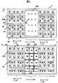
- FIG. 3 shows a top view and a bottom view of the interposer
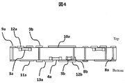
- FIG. 4 shows a cross-sectional view of the interposer.
- a layout in the case where the ground is assigned to the Top layer and the power supply is assigned to the Bottom layer is shown.
- an interposer in the case where two LSIs are arranged adjacent to each other is shown, but any number of two or more LSIs may be used, and the layout may be changed according to the number.
- the feature of the pattern of this embodiment is that it has a low impedance part on the left and right and a noise filter part on the center.
- the low impedance part has BGA ball electrodes arranged at a predetermined interval in the Top layer and the Bottom layer, and the corresponding BGA ball electrodes in the Top layer and the Bottom layer are connected via the VIA 8a.
- the top layer has a ground wiring pattern 10b and a capacitor mounting electrode 12a connected to the ground wiring pattern 10b between the BGA ball electrodes.
- the power supply wiring pattern 11a is wired between the BGA ball electrodes so as to correspond to the ground wiring pattern 10b of the Top layer.
- the power supply wiring pattern 11a is connected to the capacitor mounting electrode 12a in the top layer via the VIA 8a.
- the capacitor 3a is built in the Top layer side as shown in FIG.
- the top layer is regularly covered with a solid ground pattern 10a, and the bottom layer is regularly covered with a rectangular pattern 11b for power supply.
- a capacitor mounting electrode 12b is arranged at the center of this periodic pattern, and a capacitor is built in on the bottom side as indicated by 3b in FIG.
- chip inductances are mounted on the top, bottom, left, and right of the rectangular pattern at the positions indicated by 13a and 13b in FIG. 3 to form an electrical connection between the rectangular power supply patterns via the inductor.
- the chip inductance is mounted on the bottom side as indicated by 4a in FIG.
- the basic structure of the filter unit in FIG. 5 is based on a general EBG structure.
- a general EBG structure in a two-layer structure of a power source and a ground, the ground has a solid surface and a special periodic structure on the power source.
- This special structure consists of a structure called a small metal branch connecting a large square called a metal patch and a plurality of metal patches.
- a large metal patch forms a parallel plate with the ground, is electrically capacitive, and has a low impedance structure at high frequencies.
- the connection wiring between small metal patches called metal branches is electrically inductive and has a high impedance structure at high frequencies.
- the center frequency is determined by the capacitance of the metal patch and the inductance of the metal branch, and is inversely proportional to the square root of the product of both. .
- the noise filter effect of the present invention is shown in FIG.
- As a filter structure in the power supply pattern there is an Electromagnetic Band Gap (EBG) structure. Since the filter characteristics of the EBG configured by the wiring pattern are determined by the pattern size, the frequency of the band rejection filter is effective only in a high frequency region exceeding GHz. Don't be.
- EBG Electromagnetic Band Gap
- the low impedance part is a structure specialized for reducing the impedance of the LSI directly above, whereas this structure is a structure specialized for suppressing propagation. .
- FIG. 6 shows an enlarged view of a bird's eye view of the low impedance part of the interposer of the present invention.
- the top layer side is the semiconductor LSI mounting surface
- the bottom layer side is the mounting surface to the SiP package or PCB.
- the combination of the four terminals in FIG. 6 is the basic structure.
- the ground ball electrode 9a is previously provided on the top layer ground.
- the power supply ball electrode 9b connected to the wiring pattern 10a may be designed to be connected to the power supply wiring pattern 11a of the Bottom layer.
- the signal ball electrode 9c is not connected anywhere, and it is only necessary to connect the Top-Bottom directly with VIA.
- the same interposer can be used for various power supply, ground and signal pin arrangement targets, and the effect of cost reduction by mass production can be obtained at the time of manufacture.
- an interposer, a printed circuit board, and a semiconductor device that reduce propagation noise and realize low-cost and high-density mounting even in a high-density package / board mounted with a plurality of LSIs such as SiP. Can be provided.
- FIG. 7 shows the configuration of the interposer according to the second embodiment of the present invention.
- the package of the wiring pattern shown in FIG. 6 described in the first embodiment is prepared, and then electrically short-circuited to the ground wiring pattern 10a and the power wiring pattern 11a according to the target signal type. By doing so, characteristics such as power supply, signal, and ground are given to the electrodes.
- a rectangular pattern having a set of four terminals, one power supply terminal, one GND terminal, and two signal terminals is arranged in a lattice pattern.
- the power supply terminal and the GND terminal are arranged on a diagonal line
- the two signal terminals are arranged on another diagonal line.
- the power supply, GND, and signal terminal have corresponding BGA ball electrodes in the top layer and bottom layer of the interposer, and the corresponding BGA ball electrodes are connected via the VIA 8a.
- the GND wiring pattern 10a and the power supply wiring pattern 11a are wired between the power supply terminal and the GND terminal as in the first embodiment.
- the power supply terminal is connected to the power supply wiring pattern 11a wired in the Bottom layer by the solder short 14b in the Bottom layer.
- the GND terminal is connected to the ground wiring pattern 10a wired in the Top layer by the solder short 14a in the Top layer.
- the capacitor 3a is built in the Top layer, the capacitor 3a is connected to the capacitor mounting electrode 12a, and the capacitor mounting electrode 12a is connected to the power supply wiring pattern 11a of the Bottom layer via Via.
- An advantage of the present invention is that semiconductor LSIs having the same ball pitch and the same interposer can be used for many LSIs as long as the package size (number of balls) is the same. Due to this mass production effect, the cost of the interposer can be reduced.
- an interposer, a printed circuit board, and a semiconductor device that reduce propagation noise and realize low-cost and high-density mounting even in a high-density package / board mounted with a plurality of LSIs such as SiP. Can be provided.
- FIG. 8 shows the configuration of the interposer in the third embodiment of the present invention.
- the BGA ball electrode is connected to the ground and the power supply pattern in the Top layer and the Bottom layer, and a characteristic is given to each electrode by making a cut like 15a later and separating. This method also enables the development of a general-purpose interposer with a ball arrangement, which leads to lower costs.
- a method of incorporating a chip component as a structure for providing a capacity and an inductance is described.
- a capacitor structure using a thin film high dielectric material or a spiral inductor is configured by a wiring pattern. Similar effects may be obtained using methods.
Landscapes
- Physics & Mathematics (AREA)
- Electromagnetism (AREA)
- Engineering & Computer Science (AREA)
- Microelectronics & Electronic Packaging (AREA)
- Production Of Multi-Layered Print Wiring Board (AREA)
- Structure Of Printed Boards (AREA)
Abstract
SiPのような複数LSIを搭載したパッケージ・基板でも伝播ノイズを低減し、低コスト且つ高密度な実装を実現するインターポーザ、プリント基板及び半導体装置を提供することである。 複数の半導体LSIの間に挿入されるインターポーザであって、前記インターポーザは、電源端子、GND端子及び信号端子からなり、コンデンサを内蔵した端子構造と、前記複数の半導体LSI間のノイズ伝播を抑制するノイズフィルタ構造と、を有することを特徴とする。
Description
本発明は、インターポーザ、プリント基板及び半導体装置に関する。
本技術分野の背景技術として、特開2001-326298(特許文献1)がある。これには、「動作周波数が高い高性能LSIの電源ノイズを低減させるのに有効な低インダクタンス且つ大容量であって、しかも、低コストで信頼性が高いキャパシタを内蔵したインターポーザを実現」する手段が記載されている(要約参照)。
特許文献1には、キャパシタ内蔵インターポーザ及びその製造方法に関して記載があり、インターポーザの表面と裏面との間を貫通して形成された電源ビア、グランド・ビア、信号ビア等の複数のスルー・ビアと、スルー・ビアのピッチ間に形成され高誘電率材、電源電極面、グランド電極面が前記表面と略直交する方向に延在するキャパシタとをもつセラミックインターポーザによって解決している。
しかしながら、System in Package(SiP)のような多数のLSIを実装することが主流となりつつある現状の高密度半導体LSIでこのようなインターポーザを取り扱うには以下の課題がある。1つは、高速化・高密度化に伴う伝播ノイズの広帯域な低減が必要であることである。また、1つは、部品内蔵技術はコスト増のため、低コスト化が課題となることである。そこで、本発明の目的は、SiPのような複数LSIを搭載したパッケージ・基板でも伝播ノイズを低減し、低コスト且つ高密度な実装を実現するインターポーザ、プリント基板及び半導体装置を提供することである。
上記課題を解決するために、例えば特許請求の範囲に記載の構成を採用する。
本願は上記課題を解決する手段を複数含んでいるが、その一例を挙げるならば、複数の半導体LSIの間に挿入されるインターポーザであって、前記インターポーザは、電源端子、GND端子及び信号端子からなり、コンデンサを内蔵した端子構造と、前記複数の半導体LSI間のノイズ伝播を抑制するノイズフィルタ構造と、を有することを特徴とする構成をとるものである。
本発明によれば、SiPのような複数LSIを搭載した高密度パッケージ・基板でも伝播ノイズを低減し、低コスト且つ高密度な実装を実現するインターポーザ、プリント基板及び半導体装置を提供することができる。
上記した以外の課題、構成及び効果は、以下の実施形態の説明により明らかにされる。
以下、実施例について図面を用いて説明する。
なお、実施例を説明するための全図において、同一部には原則として同一の符号を付し、繰り返しの説明は省略する。
本実施例では、System in Package(SiP)における本発明のインターポーザの適用例を説明する。
図1は、本実施例の半導体装置の構成図の例である。 半導体装置には、複数の半導体LSIを実装したプリント回路基板(PCB)7を有し、図1はその一部分を描画している。図1では、PCB7上に複数のLSIを搭載したパッケージであるSystem inPackage(SiP)6がBGA半田ボール5bを介して実装されている。
図1ではSiP6に3つの半導体LSI 2a、2b、2Cが搭載されており、SiP6と2つのLSI2a、2bの間には、電源のノイズを低減させるためにコンデンサを内蔵したインターポーザ1が挿入されている。一般的に、LSI内の回路とコンデンサを近づけて配置することが電源ノイズを低減するために効果的であることは知られており、部品内蔵技術でチップのより近くに実装しようというのが近年の技術トレンドである。図1のように複数のLSIが実装されているパッケージあるいはPCBと複数LSIの間にインターポーザを挿入することで、高コストとなる部品内蔵技術の適用範囲を最小限にとどめる事ができるので、パッケージやPCB全体に適用する場合に比べて低コストな低雑音構造を実現できる。
本実施例のように、複数のLSIが実装されているパッケージあるいはPCBと複数LSIの間にインターポーザを挿入する場合には、高速化・高密度化に伴う伝播ノイズの広帯域な低減が必要であることであり、また、部品内蔵技術のコスト増加のため、低コスト化が課題となる。上記課題を解決する本発明のインターポーザの構成を以下に説明する。
図2は、本発明のインターポーザを簡易等価回路で表現した図である。端子の種類として信号(S)、電源(V1,V2)、グランド(G)の三種があり、信号(S)は、インターポーザの層方向の上面から下面へ直接接続され、電源(V)とグランド(G)の間において、直下の低インピーダンス部にはコンデンサ、隣接する異種チップ用電源端子間にはノイズフィルタ部があり、そこにはインダクタンスが直列に入っている。
これにより、電源(V)-グランド(G)間の上下方向は容量(C)により高周波で低インピーダンスとなり、横方向はLCフィルタにより高周波ノイズが遮蔽される。なお、容量のインピーダンスは周波数に反比例するため、周波数が高いほど低インピーダンスとなる。また、LCフィルタは2π(L/C)0.5で決まるカットオフ周波数以下では信号を通すが、それ以上では信号を通さないフィルタとなる。一方、信号(S)はインターポーザ1の層方向上下に繋がれており、他のピンとは一切電気的に接続されていないため、他の影響を受けにくい構造となっている。
図3にインターポーザの上面図と下面図を表し、図4にインターポーザの断面図を示す。ここでは、Top層にグランド、Bottom層に電源を割り当てた場合のレイアウトを示す。この例では、2つのLSIを隣接して配置する場合のインターポーザを示しているが、2つ以上であればいくつでもよく、レイアウトもこのパターンを個数に合わせて変更すればよい。
本実施例のパターンの特徴は、左右に低インピーダンス部、中央にノイズフィルタ部を有する点である。低インピーダンス部はTop層及びBottom層に所定の間隔で配置されたBGAボール電極を有し、Top層及びBottom層の対応するBGAボール電極間はVIA8aを介して接続されている。
Top層にはBGAボール電極の間にグランド配線パターン10bとグランド配線パターン10bに接続されたコンデンサ実装電極12aを有している。また、Bottom層には、電源配線パターン11aがTop層のグランド配線パターン10bと対応するようにしてBGAボール電極間に配線されている。この電源配線パターン11aはVIA8aを介してTop層のコンデンサ実装電極12aと接続されている。コンデンサ3aは図4のようにTop層側に内蔵されているものである。
また、ノイズフィルタ部は、Top層はベタのグランドパターン10a、Bottom層は電源用の矩形パターン11bが規則的に敷き詰められている。この周期的なパターンの中央にコンデンサ実装用電極12bが配置され、図4の3bのようにBottom側にコンデンサが内蔵されている。また矩形のパターンの上下左右には、図3の13a、13bに示す位置にチップインダクタンスが実装されて、インダクタを介して矩形の電源パターン間の電気的な接続を構成している。チップインダクタンスの実装は、図4の4aに示すとおり、Bottom側に内蔵されている。
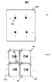
次にフィルタ部の拡大図を図5に示す。
図5のフィルタ部の基本的な構造は、一般的なEBG構造を基本としている。一般的なEBG構造では、電源とグランドの2層構造において、グランドはベタ面、電源に特殊な周期構造を有している。この特殊構造とは、メタルパッチと呼ばれる大きい正方形と複数のメタルパッチ間を接続する小サイズのメタルブランチと呼ばれる構造からなる。
大きいメタルパッチはグランドと平行平板を形成し、電気的に容量性を有し、高周波では低インピーダンス構造となる。一方、メタルブランチと呼ばれる小サイズのメタルパッチ間の接続配線は電気的にインダクタンス性を有し、高周波で高インピーダンス構造となる。この構造では、特定の周波数に対して帯域阻止フィルタの機能を持たせることが出来るが、その中心周波数はこのメタルパッチの容量とメタルブランチのインダクタンスの値で決まり、両者の積の平方根に反比例する。そのため、両者を大きくするほどより低い周波数までカバーできる構造となる
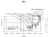
図9に本発明のノイズフィルタ効果を示す。電源パターンにおけるフィルタ構造として、Electromagnetic Band Gap(EBG)構造があるが、配線パターンで構成するEBGのフィルタ特性はパターンサイズでその帯域阻止フィルタの周波数が決まるため、GHz超の高周波領域でしか有効とならない。
図9に本発明のノイズフィルタ効果を示す。電源パターンにおけるフィルタ構造として、Electromagnetic Band Gap(EBG)構造があるが、配線パターンで構成するEBGのフィルタ特性はパターンサイズでその帯域阻止フィルタの周波数が決まるため、GHz超の高周波領域でしか有効とならない。
他方、本発明のように部品を内蔵させることで、数十MHz帯といった中周波帯まで‐60dB以下という優秀なフィルタ特性を実現することができる。チップ部品として0402や0603といった小サイズの部品を利用すれば、わずか数mm程度の空間で、高いフィルタ能力を有するパッケージを提供できる。
なお、低インピーダンス部との関係性としては、低インピーダンス部は直上のLSIのインピーダンスを低減することに特化した構造であることに対し、本構造は伝播を抑えることに特化した構造である。
これら2つを併せ持つことで、特にアナログデジタル混載パッケージのような比較的大きい電圧を扱う回路(デジタル)とノイズに対する感度が高い回路(アナログ)を近接したときに起こるミックスドシグナルノイズ問題に対して、より大きな効果が得られる。なぜならば、デジタル回路にとって誤動作の問題とならないような小さいノイズでも、アナログ回路にとっては誤動作に繋がることがあるため、それぞれのLSIのノイズを下げるだけでなく、伝播を下げるということを同時に満たすことが重用である。
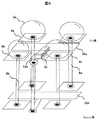
図6に本発明のインターポーザの低インピーダンス部の鳥瞰図の拡大図を示す。Top層側が半導体LSI実装面、Bottom層側がSiPパッケージまたはPCBへの実装面である。図6の4端子の組み合わせが基本構造となる。信号、電源、グランドのボール配置が常に決まっているような半導体LSI(たとえば、DRAMのようなJEDEC標準でパッケージのボール配置が決まっているもの)については、予めグランドボール電極9aはTop層のグランド配線パターン10aに接続し、電源ボール電極9bは、Bottom層の電源配線パターン11aに接続したパターン設計をすればよい。信号ボール電極9cはどこにも繋がず、Top‐Bottom間を直接VIAで繋ぐだけでよい。
このような構成をとることにより様々な電源、グランド、信号ピン配置の対象に対して同じインターポーザを利用することができ、製造時に量産による低コスト化という効果を得ることができる。
以上のことから、本発明によれば、SiPのような複数LSIを搭載した高密度パッケージ・基板でも伝播ノイズを低減し、低コスト且つ高密度な実装を実現するインターポーザ、プリント基板及び半導体装置を提供することができる。
図7に本発明の実施例2におけるインターポーザの構成を示す。
実施例2では、実施例1で説明した図6に記載の配線パターンのパッケージを作成しておき、その後、対象の信号種類に応じて、グランド配線パターン10aや電源配線パターン11aに電気的にショートさせることで、電極に電源・信号・グランドといった特性を与えたものである。
具体的には、インターポーザが有する低インピーダンス部においては、電源端子1つ、GND端子1つ、信号端子2つの4端子を1組とした矩形パターンが格子状に配されており、1組の矩形パターンにおいては、電源端子及びGND端子が対角線上に配置され、2つの信号端子が他の対角線上に配される構成をとっている。
電源、GND及び信号端子はインターポーザのTop層及びBottom層において対応するBGAボール電極を有し、それぞれの対応するBGAボール電極間はVIA8aを介して接続されている。GND配線パターン10a及び電源配線パターン11aは実施例1と同様に電源端子及びGND端子の間に配線されている。
そして、電源端子はBottom層に配線された電源配線パターン11aとBottom層で半田ショート14bによって接続されている。また、GND端子はTop層に配線されたグランド配線パターン10aとTop層で半田ショート14aによって接続されている。さらに、Top層にはコンデンサ3aが内蔵され、コンデンサ3aはコンデンサ実装電極12aと接続され、コンデンサ実装電極12aはViaを介してBottom層の電源配線パターン11aと接続されている。
このような構成をとることにより、電源・グランドは低雑音構造に接続し信号は直接的に上下に接続する効果を得ることができ、電源ノイズを低減しつつ信号の特性を劣化させないという効果を得ることができる。本発明の利点は、同じボールピッチの半導体LSIであり、パッケージサイズ(ボール数)が同じものであれば、多数のLSIについて同一のインターポーザを使いまわすことが出来る点である。これによる量産効果で、インターポーザの低コスト化が可能となる。
以上のことから、本発明によれば、SiPのような複数LSIを搭載した高密度パッケージ・基板でも伝播ノイズを低減し、低コスト且つ高密度な実装を実現するインターポーザ、プリント基板及び半導体装置を提供することができる。
図8に本発明の実施例3におけるインターポーザの構成を示す。
実施例3では、Top層、Bottom層でグランド、電源パターンにBGAボール電極を繋いでおき、後で15aのような切込みを入れて分離することで、各電極に特性を与えることである。こちらの方法でも、汎用的なボール配置でのインターポーザの開発が可能となり、低コスト化に繋がる。
なお、本明細書では、容量やインダクタンスを持たせるための構造としてチップ部品を内蔵する手法を記載したが、例えば薄膜高誘電体の利用によるコンデンサ構造や、配線パターンによりスパイラルインダクタを構成することによる方法を用いて、同様の効果を得てもよい。
1 インターポーザ
2a、2b 半導体LSI
3a、3b、3c チップコンデンサ
4a、4b チップインダクタ
5a、5b BGA(Ball Grid Array)半田ボール
6 パッケージ基板
7 プリント回路基板
8a、8b、8c スルーホール
9a、9b、9c BGAボール電極
10a、10b、 グランドプレーン、グランド配線
11a、11b、 電源プレーン、電源配線
12a、12b、 チップコンデンサ実装電極
13a、 チップインダクタ実装電極
14a、14b 半田ショート
15a、15b パターン分離切り込み
2a、2b 半導体LSI
3a、3b、3c チップコンデンサ
4a、4b チップインダクタ
5a、5b BGA(Ball Grid Array)半田ボール
6 パッケージ基板
7 プリント回路基板
8a、8b、8c スルーホール
9a、9b、9c BGAボール電極
10a、10b、 グランドプレーン、グランド配線
11a、11b、 電源プレーン、電源配線
12a、12b、 チップコンデンサ実装電極
13a、 チップインダクタ実装電極
14a、14b 半田ショート
15a、15b パターン分離切り込み
Claims (10)
- 複数の半導体LSIの間に挿入されるインターポーザであって、
前記インターポーザは、電源端子、GND端子及び信号端子からなり、コンデンサを内蔵した端子構造と、
前記複数の半導体LSI間のノイズ伝播を抑制するノイズフィルタ構造と、を有することを特徴とするインターポーザ。 - 請求項1に記載のインターポーザであって、
前記端子構造は、インターポーザ基板においてLSI実装位置の直下に内蔵したコンデンサを有することを特徴とするインターポーザ。 - 請求項1に記載のインターポーザであって、
前記端子構造は、インターポーザ基板の内層に用いた薄膜高誘電体材料により形成されることを特徴とするインターポーザ。 - 請求項1に記載のインターポーザであって、
前記ノイズフィルタ構造は、インターポーザ基板においてLSI実装位置の直下に内蔵したコンデンサ部品とインダクタンス部品により構成されることを特徴とするインターポーザ。 - 請求項1に記載のインターポーザであって、
前記ノイズフィルタ構造は、インターポーザ基板に内層に用いた薄膜高誘電体材料により
形成されたキャパシタと配線パターンで形成された、前記端子構造よりも高いインダクタンスを有する構造であることを特徴とするインターポーザ。 - 請求項1に記載のインターポーザであって、
ノイズフィルタ部は、コンデンサにより高周波でインピーダンスが低くなる構造とインダクタにより高周波でインピーダンスが高くなる構造を周期的に繰り返すパターンを持たせていることを特徴とするインターポーザ。 - 請求項1に記載のインターポーザであって、
前記端子構造は、インターポーザの上端層と下端層を接続する1つの電源端子と、1つのGND端子と、2つの電源端子とから成る4端子が矩形状に配置された1組の端子パターンが格子状に配置された構成を有し、
前記上端層には前記電源端子と前記GND端子の間にGND配線パターンが設けられ、前記下端層には前記GND配線パターンと対向するように電源配線パターンが設けられており、
前記上端層において前記GND端子は前記GND配線パターンと電気的に接続され、前記下端層において前記電源端子は前記電源パターンと電気的に接続されたことを特徴とするインターポーザ。 - 前記請求項7に記載のインターポーザであって、
前記1組の端子パターン内に前記電源配線パターンと電気的に接続され、インターポーザ上端層に設けられたコンデンサ実装電極を有し、前記コンデンサ実装電極にはコンデンサが接続されていることを特徴とするインターポーザ。 - 半導体LSIを複数搭載するプリント基板であって、
前記複数のLSIと接続された請求項1~8のいずれかに記載のインターポーザを有することを特徴とするプリント基板。 - 半導体LSIを複数搭載する半導体装置であって、
前記複数のLSIと接続された請求項1~8のいずれかに記載のインターポーザを有することを特徴とする半導体装置。
Applications Claiming Priority (2)
| Application Number | Priority Date | Filing Date | Title |
|---|---|---|---|
| JP2012-146309 | 2012-06-29 | ||
| JP2012146309A JP5852929B2 (ja) | 2012-06-29 | 2012-06-29 | インターポーザ、プリント基板及び半導体装置 |
Publications (1)
| Publication Number | Publication Date |
|---|---|
| WO2014002663A1 true WO2014002663A1 (ja) | 2014-01-03 |
Family
ID=49782830
Family Applications (1)
| Application Number | Title | Priority Date | Filing Date |
|---|---|---|---|
| PCT/JP2013/064570 Ceased WO2014002663A1 (ja) | 2012-06-29 | 2013-05-27 | インターポーザ、プリント基板及び半導体装置 |
Country Status (2)
| Country | Link |
|---|---|
| JP (1) | JP5852929B2 (ja) |
| WO (1) | WO2014002663A1 (ja) |
Cited By (2)
| Publication number | Priority date | Publication date | Assignee | Title |
|---|---|---|---|---|
| JP2017162904A (ja) * | 2016-03-08 | 2017-09-14 | ルネサスエレクトロニクス株式会社 | 半導体装置 |
| CN109817610A (zh) * | 2017-11-21 | 2019-05-28 | 环旭电子股份有限公司 | 半导体封装装置 |
Families Citing this family (7)
| Publication number | Priority date | Publication date | Assignee | Title |
|---|---|---|---|---|
| CN106663671B (zh) * | 2014-07-03 | 2021-01-22 | 高通股份有限公司 | 在晶片级封装(wlp)集成器件中实现的高品质因数滤波器 |
| JP2016119375A (ja) * | 2014-12-19 | 2016-06-30 | ホシデン株式会社 | 光電変換モジュール及びアクティブ光ケーブル |
| WO2016103359A1 (ja) | 2014-12-24 | 2016-06-30 | ルネサスエレクトロニクス株式会社 | 半導体装置 |
| JP6429647B2 (ja) | 2015-01-26 | 2018-11-28 | ルネサスエレクトロニクス株式会社 | 半導体装置 |
| JP6620885B2 (ja) | 2016-04-14 | 2019-12-18 | 株式会社村田製作所 | 複合部品内蔵回路基板、及び、複合部品 |
| WO2019123995A1 (ja) * | 2017-12-20 | 2019-06-27 | 株式会社村田製作所 | 電子部品 |
| KR102816598B1 (ko) | 2020-09-04 | 2025-06-04 | 삼성전자주식회사 | 반도체 패키지 및 그 제조 방법 |
Citations (9)
| Publication number | Priority date | Publication date | Assignee | Title |
|---|---|---|---|---|
| JPS63129655A (ja) * | 1986-11-12 | 1988-06-02 | インターナシヨナル・ビジネス・マシーンズ・コーポレーシヨン | 集積回路実装構造体 |
| JPH0582717A (ja) * | 1991-09-24 | 1993-04-02 | Toshiba Corp | 半導体集積回路装置 |
| JPH06169060A (ja) * | 1992-09-09 | 1994-06-14 | Hitachi Ltd | 電子回路装置 |
| JP2000150796A (ja) * | 1998-11-13 | 2000-05-30 | Nec Corp | 半導体装置 |
| JP2001267702A (ja) * | 2000-03-14 | 2001-09-28 | Fuji Xerox Co Ltd | プリント配線基板 |
| JP2001352004A (ja) * | 2000-06-09 | 2001-12-21 | Fujitsu Ltd | 回路基板及びその製造方法並びに半導体装置 |
| JP2004537849A (ja) * | 2001-06-28 | 2004-12-16 | スカイワークス ソリューションズ,インコーポレイテッド | リードレスマルチダイキャリアの構造およびその作製のための方法 |
| WO2007114224A1 (ja) * | 2006-03-29 | 2007-10-11 | Kyocera Corporation | 回路モジュール及び無線通信機器、並びに回路モジュールの製造方法 |
| JP2007287847A (ja) * | 2006-04-14 | 2007-11-01 | System Fabrication Technologies Inc | インターポーザ及び半導体装置 |
-
2012
- 2012-06-29 JP JP2012146309A patent/JP5852929B2/ja not_active Expired - Fee Related
-
2013
- 2013-05-27 WO PCT/JP2013/064570 patent/WO2014002663A1/ja not_active Ceased
Patent Citations (9)
| Publication number | Priority date | Publication date | Assignee | Title |
|---|---|---|---|---|
| JPS63129655A (ja) * | 1986-11-12 | 1988-06-02 | インターナシヨナル・ビジネス・マシーンズ・コーポレーシヨン | 集積回路実装構造体 |
| JPH0582717A (ja) * | 1991-09-24 | 1993-04-02 | Toshiba Corp | 半導体集積回路装置 |
| JPH06169060A (ja) * | 1992-09-09 | 1994-06-14 | Hitachi Ltd | 電子回路装置 |
| JP2000150796A (ja) * | 1998-11-13 | 2000-05-30 | Nec Corp | 半導体装置 |
| JP2001267702A (ja) * | 2000-03-14 | 2001-09-28 | Fuji Xerox Co Ltd | プリント配線基板 |
| JP2001352004A (ja) * | 2000-06-09 | 2001-12-21 | Fujitsu Ltd | 回路基板及びその製造方法並びに半導体装置 |
| JP2004537849A (ja) * | 2001-06-28 | 2004-12-16 | スカイワークス ソリューションズ,インコーポレイテッド | リードレスマルチダイキャリアの構造およびその作製のための方法 |
| WO2007114224A1 (ja) * | 2006-03-29 | 2007-10-11 | Kyocera Corporation | 回路モジュール及び無線通信機器、並びに回路モジュールの製造方法 |
| JP2007287847A (ja) * | 2006-04-14 | 2007-11-01 | System Fabrication Technologies Inc | インターポーザ及び半導体装置 |
Cited By (2)
| Publication number | Priority date | Publication date | Assignee | Title |
|---|---|---|---|---|
| JP2017162904A (ja) * | 2016-03-08 | 2017-09-14 | ルネサスエレクトロニクス株式会社 | 半導体装置 |
| CN109817610A (zh) * | 2017-11-21 | 2019-05-28 | 环旭电子股份有限公司 | 半导体封装装置 |
Also Published As
| Publication number | Publication date |
|---|---|
| JP5852929B2 (ja) | 2016-02-03 |
| JP2014011284A (ja) | 2014-01-20 |
Similar Documents
| Publication | Publication Date | Title |
|---|---|---|
| JP5852929B2 (ja) | インターポーザ、プリント基板及び半導体装置 | |
| US9468089B2 (en) | EBG structure, semiconductor device, and circuit board | |
| US6907658B2 (en) | Manufacturing methods for an electronic assembly with vertically connected capacitors | |
| US6713860B2 (en) | Electronic assembly and system with vertically connected capacitors | |
| US7679926B2 (en) | Capacitors with insulating layer having embedded dielectric rods | |
| KR100998720B1 (ko) | 전자기 밴드갭 구조물 및 인쇄회로기판 | |
| US9648794B2 (en) | Wiring board and electronic apparatus | |
| JP5694251B2 (ja) | Ebg構造体および回路基板 | |
| JP4808755B2 (ja) | 電磁気バンドギャップ構造物及び印刷回路基板 | |
| KR20080018288A (ko) | 고주파수 인쇄 회로 기판 비아 | |
| JP5750528B1 (ja) | 部品内蔵回路基板 | |
| JP6128756B2 (ja) | 半導体パッケージ、積層型半導体パッケージ及びプリント回路板 | |
| KR101046716B1 (ko) | 전자기 밴드갭 구조물 및 회로 기판 | |
| CN101610636B (zh) | 电磁带隙结构及印刷电路板 | |
| US8547681B2 (en) | Decoupling capacitor | |
| KR101018796B1 (ko) | 전자기 밴드갭 구조물 및 회로 기판 | |
| KR101444555B1 (ko) | 대역 통과 필터 | |
| US10057976B1 (en) | Power-ground co-reference transceiver structure to deliver ultra-low crosstalk | |
| JP2011066223A (ja) | 回路基板 | |
| US9431337B2 (en) | Semiconductor device having an inner power supply plate structure | |
| US8848386B2 (en) | Electronic circuit | |
| CN103414316A (zh) | 一种带电源噪声隔离的芯片封装结构 | |
| KR20140081546A (ko) | 패키지 기판 및 이를 포함하는 반도체 패키지 | |
| US6969912B2 (en) | Embedded microelectronic capacitor incorporating ground shielding layers and method for fabrication | |
| CN110299332A (zh) | 芯片封装结构 |
Legal Events
| Date | Code | Title | Description |
|---|---|---|---|
| 121 | Ep: the epo has been informed by wipo that ep was designated in this application |
Ref document number: 13808922 Country of ref document: EP Kind code of ref document: A1 |
|
| NENP | Non-entry into the national phase |
Ref country code: DE |
|
| 122 | Ep: pct application non-entry in european phase |
Ref document number: 13808922 Country of ref document: EP Kind code of ref document: A1 |