WO2014002415A1 - 撮像装置 - Google Patents
撮像装置 Download PDFInfo
- Publication number
- WO2014002415A1 WO2014002415A1 PCT/JP2013/003693 JP2013003693W WO2014002415A1 WO 2014002415 A1 WO2014002415 A1 WO 2014002415A1 JP 2013003693 W JP2013003693 W JP 2013003693W WO 2014002415 A1 WO2014002415 A1 WO 2014002415A1
- Authority
- WO
- WIPO (PCT)
- Prior art keywords
- pixel
- signal charge
- signal
- pixels
- imaging device
- Prior art date
- Legal status (The legal status is an assumption and is not a legal conclusion. Google has not performed a legal analysis and makes no representation as to the accuracy of the status listed.)
- Ceased
Links
Images












Classifications
-
- G—PHYSICS
- G01—MEASURING; TESTING
- G01C—MEASURING DISTANCES, LEVELS OR BEARINGS; SURVEYING; NAVIGATION; GYROSCOPIC INSTRUMENTS; PHOTOGRAMMETRY OR VIDEOGRAMMETRY
- G01C3/00—Measuring distances in line of sight; Optical rangefinders
- G01C3/02—Details
- G01C3/06—Use of electric means to obtain final indication
- G01C3/08—Use of electric radiation detectors
- G01C3/085—Use of electric radiation detectors with electronic parallax measurement
-
- G—PHYSICS
- G01—MEASURING; TESTING
- G01B—MEASURING LENGTH, THICKNESS OR SIMILAR LINEAR DIMENSIONS; MEASURING ANGLES; MEASURING AREAS; MEASURING IRREGULARITIES OF SURFACES OR CONTOURS
- G01B11/00—Measuring arrangements characterised by the use of optical techniques
- G01B11/02—Measuring arrangements characterised by the use of optical techniques for measuring length, width or thickness
- G01B11/026—Measuring arrangements characterised by the use of optical techniques for measuring length, width or thickness by measuring distance between sensor and object
-
- G—PHYSICS
- G01—MEASURING; TESTING
- G01C—MEASURING DISTANCES, LEVELS OR BEARINGS; SURVEYING; NAVIGATION; GYROSCOPIC INSTRUMENTS; PHOTOGRAMMETRY OR VIDEOGRAMMETRY
- G01C11/00—Photogrammetry or videogrammetry, e.g. stereogrammetry; Photographic surveying
- G01C11/04—Interpretation of pictures
-
- G—PHYSICS
- G01—MEASURING; TESTING
- G01C—MEASURING DISTANCES, LEVELS OR BEARINGS; SURVEYING; NAVIGATION; GYROSCOPIC INSTRUMENTS; PHOTOGRAMMETRY OR VIDEOGRAMMETRY
- G01C11/00—Photogrammetry or videogrammetry, e.g. stereogrammetry; Photographic surveying
- G01C11/04—Interpretation of pictures
- G01C11/30—Interpretation of pictures by triangulation
-
- H—ELECTRICITY
- H04—ELECTRIC COMMUNICATION TECHNIQUE
- H04N—PICTORIAL COMMUNICATION, e.g. TELEVISION
- H04N13/00—Stereoscopic video systems; Multi-view video systems; Details thereof
- H04N13/10—Processing, recording or transmission of stereoscopic or multi-view image signals
- H04N13/106—Processing image signals
- H04N13/128—Adjusting depth or disparity
-
- H—ELECTRICITY
- H04—ELECTRIC COMMUNICATION TECHNIQUE
- H04N—PICTORIAL COMMUNICATION, e.g. TELEVISION
- H04N13/00—Stereoscopic video systems; Multi-view video systems; Details thereof
- H04N13/20—Image signal generators
- H04N13/204—Image signal generators using stereoscopic image cameras
- H04N13/254—Image signal generators using stereoscopic image cameras in combination with electromagnetic radiation sources for illuminating objects
-
- H—ELECTRICITY
- H04—ELECTRIC COMMUNICATION TECHNIQUE
- H04N—PICTORIAL COMMUNICATION, e.g. TELEVISION
- H04N13/00—Stereoscopic video systems; Multi-view video systems; Details thereof
- H04N13/20—Image signal generators
- H04N13/271—Image signal generators wherein the generated image signals comprise depth maps or disparity maps
-
- H—ELECTRICITY
- H04—ELECTRIC COMMUNICATION TECHNIQUE
- H04N—PICTORIAL COMMUNICATION, e.g. TELEVISION
- H04N13/00—Stereoscopic video systems; Multi-view video systems; Details thereof
- H04N13/20—Image signal generators
- H04N13/296—Synchronisation thereof; Control thereof
-
- H—ELECTRICITY
- H04—ELECTRIC COMMUNICATION TECHNIQUE
- H04N—PICTORIAL COMMUNICATION, e.g. TELEVISION
- H04N23/00—Cameras or camera modules comprising electronic image sensors; Control thereof
- H04N23/20—Cameras or camera modules comprising electronic image sensors; Control thereof for generating image signals from infrared radiation only
-
- H—ELECTRICITY
- H04—ELECTRIC COMMUNICATION TECHNIQUE
- H04N—PICTORIAL COMMUNICATION, e.g. TELEVISION
- H04N23/00—Cameras or camera modules comprising electronic image sensors; Control thereof
- H04N23/56—Cameras or camera modules comprising electronic image sensors; Control thereof provided with illuminating means
-
- H—ELECTRICITY
- H04—ELECTRIC COMMUNICATION TECHNIQUE
- H04N—PICTORIAL COMMUNICATION, e.g. TELEVISION
- H04N23/00—Cameras or camera modules comprising electronic image sensors; Control thereof
- H04N23/60—Control of cameras or camera modules
- H04N23/667—Camera operation mode switching, e.g. between still and video, sport and normal or high- and low-resolution modes
-
- H—ELECTRICITY
- H04—ELECTRIC COMMUNICATION TECHNIQUE
- H04N—PICTORIAL COMMUNICATION, e.g. TELEVISION
- H04N23/00—Cameras or camera modules comprising electronic image sensors; Control thereof
- H04N23/70—Circuitry for compensating brightness variation in the scene
- H04N23/73—Circuitry for compensating brightness variation in the scene by influencing the exposure time
-
- H—ELECTRICITY
- H04—ELECTRIC COMMUNICATION TECHNIQUE
- H04N—PICTORIAL COMMUNICATION, e.g. TELEVISION
- H04N23/00—Cameras or camera modules comprising electronic image sensors; Control thereof
- H04N23/70—Circuitry for compensating brightness variation in the scene
- H04N23/74—Circuitry for compensating brightness variation in the scene by influencing the scene brightness using illuminating means
-
- H—ELECTRICITY
- H04—ELECTRIC COMMUNICATION TECHNIQUE
- H04N—PICTORIAL COMMUNICATION, e.g. TELEVISION
- H04N25/00—Circuitry of solid-state image sensors [SSIS]; Control thereof
- H04N25/40—Extracting pixel data from image sensors by controlling scanning circuits, e.g. by modifying the number of pixels sampled or to be sampled
- H04N25/46—Extracting pixel data from image sensors by controlling scanning circuits, e.g. by modifying the number of pixels sampled or to be sampled by combining or binning pixels
-
- H—ELECTRICITY
- H04—ELECTRIC COMMUNICATION TECHNIQUE
- H04N—PICTORIAL COMMUNICATION, e.g. TELEVISION
- H04N25/00—Circuitry of solid-state image sensors [SSIS]; Control thereof
- H04N25/50—Control of the SSIS exposure
- H04N25/57—Control of the dynamic range
- H04N25/58—Control of the dynamic range involving two or more exposures
- H04N25/587—Control of the dynamic range involving two or more exposures acquired sequentially, e.g. using the combination of odd and even image fields
-
- H—ELECTRICITY
- H04—ELECTRIC COMMUNICATION TECHNIQUE
- H04N—PICTORIAL COMMUNICATION, e.g. TELEVISION
- H04N25/00—Circuitry of solid-state image sensors [SSIS]; Control thereof
- H04N25/70—SSIS architectures; Circuits associated therewith
- H04N25/703—SSIS architectures incorporating pixels for producing signals other than image signals
- H04N25/705—Pixels for depth measurement, e.g. RGBZ
-
- H—ELECTRICITY
- H04—ELECTRIC COMMUNICATION TECHNIQUE
- H04N—PICTORIAL COMMUNICATION, e.g. TELEVISION
- H04N25/00—Circuitry of solid-state image sensors [SSIS]; Control thereof
- H04N25/70—SSIS architectures; Circuits associated therewith
- H04N25/71—Charge-coupled device [CCD] sensors; Charge-transfer registers specially adapted for CCD sensors
- H04N25/713—Transfer or readout registers; Split readout registers or multiple readout registers
-
- G—PHYSICS
- G01—MEASURING; TESTING
- G01C—MEASURING DISTANCES, LEVELS OR BEARINGS; SURVEYING; NAVIGATION; GYROSCOPIC INSTRUMENTS; PHOTOGRAMMETRY OR VIDEOGRAMMETRY
- G01C11/00—Photogrammetry or videogrammetry, e.g. stereogrammetry; Photographic surveying
- G01C11/36—Videogrammetry, i.e. electronic processing of video signals from a single source or from different sources to give parallax or range information
-
- H—ELECTRICITY
- H04—ELECTRIC COMMUNICATION TECHNIQUE
- H04N—PICTORIAL COMMUNICATION, e.g. TELEVISION
- H04N13/00—Stereoscopic video systems; Multi-view video systems; Details thereof
- H04N2013/0074—Stereoscopic image analysis
- H04N2013/0081—Depth or disparity estimation from stereoscopic image signals
Definitions
- the present invention relates to an imaging device that converts incident light into an electrical signal and outputs the signal as a video signal.
- Patent Document 1 discloses a ranging camera having a function of measuring a distance to a subject using infrared light.
- a solid-state imaging device used for a ranging camera is called a ranging sensor.
- a camera that is mounted on a game machine and detects a movement of a person's body or a hand that is a subject is also called a motion camera.
- Patent Document 2 discloses a solid-state imaging device having a vertical transfer electrode structure that enables simultaneous readout of all pixels. Specifically, it is a CCD (Charge Coupled Device) image sensor in which a vertical transfer unit extending in the vertical direction is provided next to each column of photodiodes (PD).
- the vertical transfer unit includes four vertical transfer electrodes corresponding to each photodiode, and at least one of the vertical transfer electrodes also serves as a read electrode for reading signal charges from the photodiode to the vertical transfer unit.
- a vertical overflow drain (VOD) is provided for sweeping out signal charges of all pixels of the photodiode.
- An object of the present invention is to provide an imaging apparatus for efficiently obtaining a high-precision distance image.
- an imaging apparatus is an imaging apparatus including an infrared light source that irradiates a subject with infrared light and a solid-state imaging device that receives incident light from the subject.
- the solid-state imaging device includes a plurality of first pixels and a plurality of second pixels which are arranged in a matrix on a substrate and convert incident light into signal charges, and the first and second pixels.
- a readout unit that discharges the signal charges simultaneously or independently from the photoelectric conversion unit provided in each pixel to the vertical transfer unit, and the vertical transfer unit includes a plurality of electrodes per pixel and stores one signal per pixel.
- All pixels can be read out, and signal charges can be transferred in both the upper and lower directions in the column direction, and can be obtained from the first pixel in the first exposure period within one frame scanning period. And the signal charge adjacent to the first pixel.
- the signal charge obtained from the second pixel is added on the vertical transfer unit to form a first signal charge, and the signal charge obtained from the first pixel in the second exposure period and the first charge
- the vertical transfer unit is transferred to another packet so that the signal charge obtained from the second pixel adjacent to the second pixel is not added to the first signal charge on the vertical transfer unit.
- the drive for adding as the second signal charge is output after being repeated a plurality of times.
- the signal charge irradiated with infrared light from the same two pixels and the signal charge of only the infrared light component in the background light are obtained. Since the data can be read out, two signals can be subtracted without causing a pixel shift. Further, since the signal charge is read from all the pixels in each exposure period, the utilization rate of the signal charge becomes 100%. Furthermore, since reading is performed a plurality of times within one frame period, the time difference between the two signal charges is reduced, and a moving subject can be imaged.
- an imaging apparatus that can suppress power and heat generation of the entire system while maintaining high image quality and high accuracy by changing a driving method for imaging a distance image by infrared light irradiation.
- FIG. 6 is a first timing chart in the TOF type distance measuring camera.
- A) And (b) is a figure explaining the principle of operation of the TOF type ranging camera based on the timing chart of FIG. FIG.
- FIG. 6 is a second timing chart in the TOF type distance measuring camera.
- A) And (b) is a figure explaining the principle of operation of the TOF type ranging camera based on the timing diagram of FIG.
- FIG. 10 is a third timing chart in the TOF type distance measuring camera.
- A) And (b) is a figure explaining the principle of operation of the TOF type ranging camera based on the timing diagram of FIG.
- FIG. 10 is a fourth timing chart in the TOF type distance measuring camera.
- FIG. 10 is a third timing chart in the TOF type distance measuring camera.
- A) And (b) is a figure explaining the principle of operation of the TOF type ranging camera based on the timing diagram of FIG.
- FIG. 10 is a fourth timing chart in the TO
- FIG. 16 is a drive timing chart of the solid-state imaging device of FIG. 15.
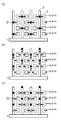
- (A), (b), (c) and (d) are conceptual diagrams showing the flow of signal charges within one frame period of the solid-state imaging device of FIG. It is a block diagram of the solid-state imaging device which concerns on the 2nd Embodiment of this invention. It is a drive timing diagram of the solid-state imaging device of FIG. (A) And (b) is a conceptual diagram which shows the flow of the signal charge within 1 frame period of the solid-state imaging device of FIG. (A) And (b) is a conceptual diagram which shows the flow of the signal charge in 1 frame period in the modification of the solid-state imaging device of FIG.
- FIG. 1 It is a block diagram of the solid-state imaging device which concerns on the 3rd Embodiment of this invention.
- (A), (b), (c) and (d) are conceptual diagrams showing the flow of signal charges within one frame period of the solid-state imaging device of FIG. It is a block diagram of the solid-state imaging device which concerns on the 4th Embodiment of this invention.
- (A) And (b) is a conceptual diagram which shows the flow of the signal charge within 1 frame period of the solid-state imaging device of FIG. It is a block diagram of the solid-state imaging device which concerns on the 5th Embodiment of this invention. It is a drive timing diagram of the solid-state imaging device of FIG.
- FIG. 31 is a drive timing chart of the solid-state imaging device of FIG. 30.
- (A), (b), and (c) are the conceptual diagrams which show the flow of the signal charge in 1 frame period of the solid-state imaging device of FIG.
- FIG. 1 is a diagram showing a schematic configuration of a ranging camera equipped with a solid-state imaging device according to the present invention.
- an infrared laser beam having a wavelength of 850 nm is irradiated from an infrared light source 103 to a subject 101 in a photographing target space 100 under background light illumination 102.
- the reflected light is received by the solid-state imaging device 106 via the optical lens 104 and the optical filter 105 that transmits the near-infrared wavelength region near 850 nm, and the image formed on the solid-state imaging device 106 is converted into an electrical signal.
- the infrared light source 103, the optical lens 104, the optical filter 105, and the solid-state imaging device 106 that is, for example, a CCD image sensor constitute a distance measuring camera.
- ranging cameras There are several types of ranging cameras, but any of a stereo system, a pattern irradiation type, a TOF (Time Of Flight) type, etc. may be used.
- FIG. 2 is a diagram for explaining a distance measuring method of a stereo distance measuring camera.
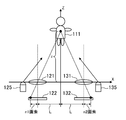
- One set of camera 120 and infrared light source 125 and another set of camera 130 and infrared light source 135 are arranged for the subject 111 in the shooting target space 110.
- the distance between the optical axes of both cameras 120 and 130 is 2L. L is called the baseline length.
- FIG. 3 is a diagram for explaining the operating principle of a stereo distance measuring camera.
- the infrared light sources 125 and 135 each irradiate the subject 111 with infrared light.
- One camera 120 includes a lens 121 and a solid-state imaging device 122, and an infrared light spot forms an image at a position separated by n1 pixels from the center.
- the other camera 130 includes a lens 131 and a solid-state imaging device 132, and an infrared light spot forms an image at a position separated by n2 pixels from the center. Based on these results, the distance z to the subject 111 is obtained by triangulation.
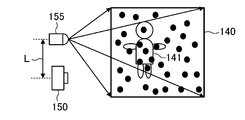
- FIG. 4 is a diagram for explaining a distance measuring method of the pattern irradiation type distance measuring camera.
- a set of cameras 150 and an infrared light source 155 are arranged for the subject 141 in the shooting target space 140.
- the infrared light source 155 irradiates the imaging target space 140 including the subject 141 with infrared light in a specific pattern.
- the baseline length is L.
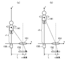
- FIG. 5A and FIG. 5B are diagrams for explaining the operation principle of the pattern irradiation type distance measuring camera.
- the camera 150 includes a lens 151 and a solid-state imaging device 152, and obtains the distance to the subject 141 based on the positional deviation amount (difference between z1 and z2) of each irradiation pattern.
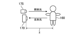
- FIG. 6 is a diagram for explaining a distance measuring method of the TOF type distance measuring camera.
- a pair of cameras 170 and an infrared light source 175 are arranged for the subject 160.
- the infrared light source 175 gives pulsed irradiation light to the subject 160 at a position separated by a distance z.
- the infrared light hitting the subject 160 is reflected.
- the camera 170 receives the reflected light.
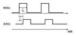
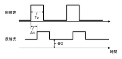
- FIG. 7 is a first timing chart of the TOF type ranging camera.
- the pulse width of the irradiation light is Tp, and the delay between the irradiation light and the reflected light is ⁇ t.
- FIG. 8A and FIG. 8B are diagrams for explaining the operating principle of the TOF type ranging camera based on the timing chart of FIG. Hereinafter, it is referred to as a first TOF method.
- the magnitude of the first signal obtained by the camera 170 is the amount of signal charge IR1 based on the reflected light in the first exposure period starting from the rising time of the irradiation light pulse.
- the magnitude of the second signal obtained by the camera 170 is the amount of signal charge IR2 based on the reflected light in the second exposure period starting from the falling time of the irradiation light pulse. .
- the length of the first and second exposure periods is set wider than the pulse width Tp of the irradiation light.
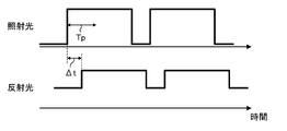
- FIG. 9 is a second timing chart in the TOF type ranging camera. Here, it is assumed that the pulse width of the irradiation light is longer than the time Tp.
- FIGS. 10A and 10B are diagrams for explaining the operating principle of the TOF type ranging camera based on the timing chart of FIG. Hereinafter, it is referred to as a second TOF method.
- the magnitude of the first signal obtained by the camera 170 is the signal charge based on the reflected light in the first exposure period (length Tp) starting after the rising time of the reflected light pulse. Amount of IR1.
- the magnitude of the second signal obtained by the camera 170 is the signal charge based on the reflected light in the second exposure period (length Tp) starting from the rising time of the irradiation light pulse.
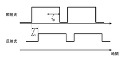
- FIG. 11 is a third timing chart of the TOF type ranging camera. Here again, it is assumed that the pulse width of the irradiation light is longer than the time Tp.
- the magnitude of the first signal obtained by the camera 170 is the signal charge based on the reflected light in the first exposure period (length Tp) that ends at the falling time of the irradiation light pulse.
- the quantity IR1 is the magnitude of the second signal obtained by the camera 170 based on the reflected light in the second exposure period (length Tp) starting from the falling time of the irradiation light pulse.
- the second TOF method that uses only the rising portion of the irradiation light pulse and the third TOF method that uses only the falling portion of the irradiation light pulse have advantages over the first TOF method. .
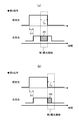
- FIG. 13 is a fourth timing chart in the TOF type ranging camera.
- the pulse width of the irradiated light is Tp
- the delay between the irradiated light and the reflected light is ⁇ t
- the background light component included in the reflected light is BG.
- FIG. 14 (a) and 14 (b) are diagrams for explaining the operating principle of the TOF type ranging camera based on the timing chart of FIG. Hereinafter, it is referred to as a fourth TOF method. Since the reflected light includes the background light component BG, it is desirable to remove the background light component BG when calculating the distance z. Therefore, a solid-state imaging device that stores three different signal charges is used.
- the amount of signal charge based on the reflected light in the first exposure period starting from the rising time of the irradiation light pulse is S0 + BG.
- the amount of signal charge based only on background light in the third exposure period in which infrared light is not irradiated is BG. Therefore, by taking the difference between the two, the magnitude of the first signal obtained by the camera 170 is S0.
- the amount of signal charge based on the reflected light in the second exposure period starting from the falling time of the irradiation light pulse is S1 + BG.
- FIG. 15 is a configuration diagram of the solid-state imaging device according to the first embodiment of the present invention. Here, for simplification of the drawing, only four pixels in the vertical direction and four pixels in the horizontal direction are shown.
- This solid-state imaging device is arranged in a matrix on a semiconductor substrate, and is provided corresponding to a plurality of photoelectric conversion units (photodiodes) 4 that convert incident light into signal charges, and the photoelectric conversion unit 4.
- a vertical transfer unit 5 that transfers the signal charges read from the column direction (vertical direction)
- a horizontal transfer unit 10 that transfers the signal charges transferred by the vertical transfer unit 5 in the row direction (horizontal direction)
- the charge detection unit 11 that outputs the signal charge transferred by the transfer unit 10, and the first read electrode 8 a and the first read electrode 8 a provided corresponding to each of the photoelectric conversion units 4 so as to be able to read each row. 2 readout electrodes 8b.
- the solid-state imaging device is an interline transfer type CCD that supports all-pixel readout (progressive scan).
- the vertical transfer unit 5 is a four-phase drive in which four vertical transfer electrodes 8 are provided per pixel.
- the horizontal transfer unit 10 is a two-phase drive.
- the signal charge readout electrode from the photoelectric conversion unit 4 has a configuration in which the vertical transfer electrodes 8a and 8b of the vertical transfer unit 5 of the four-phase drive are also used.
- the signal charge accumulated in the photoelectric conversion unit 4 is read and transferred to the electrode represented by the signal packet 9.
- Each pixel is provided with a VOD 12 for sweeping out signal charges of all the pixels.
- the VOD 12 is described in the horizontal direction of the pixel, but in reality, it is configured in the bulk direction of the pixel (the depth direction of the semiconductor substrate).
- FIG. 16 shows an example of drive timing for vertically transferring and adding two vertically adjacent pixels within one frame period.
- FIGS. 17A to 17D show charge addition and charge transfer. The image is shown.
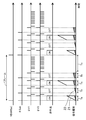
- the vertical synchronizing pulse VD is 60 frames per second (60 fps), and within each frame period, the signal charge 21 under infrared light irradiation, the signal charge 22 in the case of only background light, and Both signal charges are obtained.
- imaging with irradiation with infrared light and imaging with only background light are performed twice per frame.
- a substrate discharge pulse ( ⁇ Sub) is applied to discharge signal charges of all pixels.
- the first infrared light irradiation exposure period Ta is started, and at the same time, infrared light is irradiated. Since the background light continues to be lit, the reflected light from the subject includes both irradiated infrared light and background light.
- a readout pulse is applied to ⁇ V1A, the signal charge 21 is read out to the vertical transfer section 5, and the first exposure period Ta ends. At the same time, irradiation with infrared light is stopped. An image of charge readout from the photoelectric conversion unit 4 to the vertical transfer unit 5 at this time is also indicated by an arrow from the photoelectric conversion unit 4 in FIG.
- the infrared light irradiation period and the exposure period Ta are matched, but there is no particular problem if the infrared light irradiation period does not include the background light exposure period Tb.
- the read signal charge 21 is transferred in the forward transfer direction (downward in the figure) to one adjacent pixel by one pixel. Then, a read pulse is applied to ⁇ V1B, and the signal charge is read out to the vertical transfer unit 5. At this time, it is added to the signal charge that has already been read out from ⁇ V1A. The added signal charge 21 is vertically transferred in the reverse transfer direction (upward in the figure) by one pixel, contrary to the previous case.
- a read pulse is applied to ⁇ V1B, and the signal charge 22 of the background light component accumulated in the photoelectric conversion unit 4 is read to the vertical transfer unit 5 as shown in FIG. In that case, it reads to another packet so that it may not add with the signal charge 21 containing the irradiation infrared light previously.
- the signal charges 21 and the signal charges 22 are returned to the same positions as in FIG. 17A, the signal charge 22 is not shown, but as shown in FIG. 17D, an empty packet sandwiched between the signal charges 21 corresponds to the position of the signal charge 22.
- the infrared light irradiation ON / OFF and the series of driving shown in FIGS. 17A to 17D are set as one set. At the driving timing shown in FIG. 16, two sets are performed within one frame period and then transferred. It is output in the period Tc.
- the signal charge 21 obtained by irradiating infrared light from two pixels adjacent in the vertical direction and the signal charge 22 of only the background light are used. This makes it possible to obtain a signal of 2 and eliminates a pixel shift between the two signals. Thereby, when background light is subtracted using two signals, signals obtained from the same address are subtracted from each other, so that it is possible to accurately acquire a distance image. In addition, the design of the pixel portion is easy.
- the solid-state imaging device since signal charges accumulated in all photodiodes are used by adjacent addition, there is no signal charge to be swept away on the substrate, and the utilization rate can be 100%. it can.
- the output of the irradiating infrared light source can be lowered or the exposure period can be shortened if the same amount of infrared light signal is required. That is, it is effective for reducing power consumption.
- the driving for reading out the signal charge 21 irradiated with infrared light twice and the signal charge 22 of only the background light is repeated twice within one frame period, the time difference between the two signals is substantially shortened. Even when a fast-moving subject is imaged and background light is subtracted using two signals, errors are less likely to occur.
- the arrangement of signals output in the signal charge transfer period Tc is the same as that in the prior art, and the existing system can be used as the signal processing system. It can be easily handled by replacing the imaging device. That is, it has high affinity with existing systems.
- the solid-state imaging device according to the first embodiment is mainly used as a stereo or pattern irradiation type distance measuring sensor.
- the solid-state imaging device according to the second embodiment of the present invention will be described focusing on differences from the first embodiment.
- the solid-state imaging device according to the second embodiment differs from the solid-state imaging device according to the first embodiment in a method of reading signal charges from two adjacent pixels, and further, due to this, a vertical transfer unit The configuration is different.
- vertical direction is the same as that of the solid-state imaging device which concerns on 1st Embodiment.
- the description will focus on the points different from the first embodiment, and the description of the same points will be omitted.
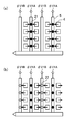
- FIG. 18 is a configuration diagram of a solid-state imaging device according to the second embodiment.
- this solid-state imaging device reads signal charges from the photoelectric conversion unit 4 to the vertical transfer unit 5 provided corresponding to the photoelectric conversion unit 4.
- the electrodes are different, and the readout electrodes of two adjacent pixels are approaching as compared with the solid-state imaging device of FIG. 15 according to the first embodiment.
- every fourth readout electrode is arranged in the vertical transfer electrode, but in the solid-state imaging device of FIG. 18 according to the present embodiment, the readout electrode of the signal charge from the photoelectric conversion unit 4 is ⁇ V1 and As in ⁇ V3, two readout electrodes 8a and 8b are arranged at a distance of two electrodes.
- FIG. 19 shows an example of the drive timing for adding two vertically adjacent pixels within one frame period. Compared to FIG. 16 of the first embodiment, ⁇ V1 and ⁇ V3 are applied simultaneously. Is different.
- the signal of the exposure period irradiated with infrared light is read out as signal charges 21 to the vertical transfer section 5 by simultaneously applying read pulses to ⁇ V1 and ⁇ V3.
- the signals of two pixels are added in one signal packet.
- the added signal charge 21 is vertically transferred by one pixel in the reverse transfer direction (upward in the figure), and after the signal charges of all the pixels are discharged at ⁇ Sub, the signal charge 22 accumulated in the exposure period Tb is Similarly, by simultaneously applying a read pulse to ⁇ V1 and ⁇ V3, a signal charge 22 read and added to another packet of the vertical transfer unit 5 is obtained.
- the timing for reading from two adjacent pixels is the same, so that it is possible to calculate the distance more accurately in addition to the design of the drive timing being facilitated. It becomes possible. It is also possible to use a distance measuring method such as a TOF type distance measuring sensor that leads to erroneous determination of distance if a time difference occurs between two signals to be added.
- the order of signals to be output is the same as that shown in the first embodiment, and the signal processing system can use an existing system. Therefore, the solid-state imaging device of this embodiment is also the first embodiment. Similar to the embodiment, it can be easily replaced by replacing the conventional solid-state imaging device.
- the solid-state imaging device according to the third embodiment of the present invention Compared with the solid-state imaging device according to the first embodiment, the solid-state imaging device according to the third embodiment has a checkered pattern in which the arrangement of the readout electrodes ⁇ V1A and ⁇ V1B is shifted by one pixel for each column. Is different.
- vertical direction is the same as that of the solid-state imaging device which concerns on 1st Embodiment.
- the description will focus on the points different from the first embodiment, and the description of the same points will be omitted.
- FIG. 22 is a configuration diagram of a solid-state imaging device according to the third embodiment. Compared with the solid-state imaging device of FIG. 15 according to the first embodiment, this solid-state imaging device reads signal charges from the photoelectric conversion unit 4 to the vertical transfer unit 5 provided corresponding to the photoelectric conversion unit 4.
- the pixel on the right side of the pixel having the readout electrode of ⁇ V1A similarly has the readout electrode of ⁇ V1A.
- the solid-state imaging device of FIG. 22 according to this embodiment is different in that a pixel having a readout electrode of ⁇ V1B is arranged on the right side of a pixel having a readout electrode of ⁇ V1A.
- a pixel having a read electrode of ⁇ V1A is arranged on the right side of the pixel having a read electrode of ⁇ V1B.
- the pixel in the lower row is the opposite, and the leftmost pixel has a readout electrode of ⁇ V1B, and the pixel on the right side has a readout electrode of ⁇ V1A.
- the pixels having the ⁇ V1A readout electrode and the pixels having the ⁇ V1B readout electrode are arranged in a checkered pattern.
- the signal charge 21 obtained in the exposure period irradiated with infrared light and the exposure period in the background light state without irradiation with infrared light were obtained.
- the signal charges 22 are output in a checkered pattern.
- FIG. 23A for easy understanding, in the photoelectric conversion unit 4, a pixel read by ⁇ V1A is described as “A”, and a pixel read by ⁇ V1B is described as “B”.
- the infrared light irradiation ON / OFF and the series of driving shown in FIGS. 23A to 23D are set as one set, and the driving timing shown in FIG. 16 according to the first embodiment is within one frame period. Are output in the transfer period Tc.
- the solid-state imaging device by subtracting the signal charge obtained without irradiating infrared light from the signal charge obtained by irradiating infrared light, Even if the resolution is reduced by half, the signal after the subtraction is checkered, so that the resolution can be complemented by signal processing. As a result, higher-definition distance measurement is possible than with a conventional distance measurement sensor having the same number of pixels.
- a solid-state imaging device according to the fourth embodiment of the present invention will be described focusing on differences from the second embodiment.
- the solid-state imaging device according to the fourth embodiment has different combinations of two pixels to be added at the same time for each column. Is different.
- vertical direction is the same as that of the solid-state imaging device concerning 2nd Embodiment.
- the description will focus on the points different from the second embodiment, and the description of the same points will be omitted.
- FIG. 24 is a configuration diagram of a solid-state imaging device according to the fourth embodiment.
- this solid-state imaging device reads signal charges from the photoelectric conversion unit 4 to the vertical transfer unit 5 provided corresponding to the photoelectric conversion unit 4.
- the electrodes are different for each column.
- the pixel arranged at the bottom left is read out with ⁇ V3, and the pixel adjacent to the right is read out with ⁇ V3.
- the pixel arranged at the lower left is read by ⁇ V3, while the pixel on the right side is read by ⁇ V1. Furthermore, the pixel on the right is read out with ⁇ V3.
- the drive timing of the solid-state imaging device according to the fourth embodiment is The drive timing according to the second embodiment is the same as the example shown in FIG.
- FIGS. 25A and 25B the signal charge 21 obtained in the exposure period irradiated with infrared light and the exposure period in the background light state obtained without irradiating infrared light were obtained.
- the signal charges 22 are output in a checkered pattern.
- FIG. 25A for easy understanding, the pixel read by ⁇ V1 is described as “1” and the pixel read by ⁇ V3 is described as “3” in the photoelectric conversion unit 4.
- FIGS. 25 (a) to 25 (b) As in FIGS. 20 (a) to 20 (b) according to the second embodiment, the infrared light was irradiated.
- the signal charge 21 is read out and then vertically transferred, and then the signal charge 22 obtained only with the background light is read out. Note that the image of charge readout from the photoelectric conversion unit 4 to the vertical transfer unit 5 at the time of FIG. 25A is also indicated by the arrow from the photoelectric conversion unit 4 in FIG.
- the infrared light irradiation ON / OFF and the series of driving shown in FIGS. 25A and 25B are set as one set, and the driving timing shown in FIG. 19 according to the second embodiment is within one frame period. Are output in the transfer period Tc.
- the solid-state imaging device according to the fourth embodiment, by subtracting the signal charge obtained without irradiating infrared light from the signal charge obtained by irradiating infrared light, Even if the resolution is reduced by half, the signal after the subtraction is checkered, so that the resolution can be complemented by signal processing. As a result, higher-definition distance measurement is possible than with a conventional distance measurement sensor having the same number of pixels.
- the timing of reading from two adjacent pixels is the same, so that the drive timing can be easily designed, and in addition, the TOF type distance sensor is particularly effective because of the simultaneousness of addition. It is.
- the second TOF method shown in FIGS. 10 (a) and 10 (b) for calculating the distance at the rising portion of the light source pulse and FIG. 12 (a) and FIG. 12 (a) for calculating the distance at the falling portion of the light source pulse.
- the third TOF method shown in FIG. 12B is also effective.
- the second embodiment is used when it is desired to perform all pixel output (all pixel independent reading) once per frame without adding driving of two adjacent pixels.
- ⁇ V2 from ⁇ V1 and ⁇ V3 while keeping ⁇ V2 at the LOW level
- ⁇ V2 at the LOW level
- a solid-state imaging device according to the fifth embodiment of the present invention will be described focusing on differences from the fourth embodiment.
- the solid-state imaging device according to the fifth embodiment is different from the solid-state imaging device according to the fourth embodiment in the combination of two pixels to be added at the same time. Due to this, the configuration of the readout electrode is different.
- the point which aims at providing the structure which can add the signal charge of adjacent pixels is the same as that of the solid-state imaging device concerning 4th Embodiment.
- the description will be focused on the points different from the fourth embodiment, and the description of the same points will be omitted.
- FIG. 26 is a configuration diagram of a solid-state imaging device according to the fifth embodiment. Compared with the solid-state imaging device of FIG. 24 according to the fourth embodiment, this solid-state imaging device reads signal charges from the photoelectric conversion unit 4 to the vertical transfer unit 5 provided corresponding to the photoelectric conversion unit 4.
- the electrode is configured to be able to read simultaneously from each of the photoelectric conversion units 4 that are adjacent in the horizontal direction with the vertical transfer unit 5 interposed therebetween.
- FIG. 27 shows an example of drive timing for simultaneously adding two horizontally adjacent pixels within one frame period.
- FIGS. 28A to 28C show images of charge addition and charge transfer. Show.
- the signal charge is accumulated by irradiating with infrared light, a read pulse is applied to ⁇ V1, and the signal charge 21 is read in a checkered pattern as shown in FIG. Take an image.
- An image of charge readout from the photoelectric conversion unit 4 to the vertical transfer unit 5 at this time is also indicated by an arrow from the photoelectric conversion unit 4 in FIG.
- the read signal charge 21 is transferred in the reverse transfer direction (upward in the figure) to one adjacent pixel by one pixel.
- the signal charge stored in the vertical transfer unit 5 is transferred by one pixel in the forward transfer direction (downward in the figure), and the exposure period indicated by Ta in FIG. 27 starts again. .
- the subsequent flow is the same as the flow of FIGS. 28A to 28C, and this is set as one set, and at the drive timing of FIG. 27, infrared light irradiation ON / OFF and FIGS. 28A to 28 are performed.
- the series of driving in (c) is repeated two sets, the data is output in the transfer period Tc.
- the vertical transfer unit 5 can perform addition only by reading from two pixels adjacent in the horizontal direction through one common readout electrode ⁇ V1.
- the electrode structure can be read from the vicinity of the center of the photoelectric conversion unit 4. Therefore, the signal charge can be easily read out, the design is easy, and the readable voltage can be kept low.
- a solid-state imaging device as shown in FIG. 29 may be used. Compared with the solid-state imaging device shown in FIG. 26, the solid-state imaging device of FIG. 29 is arranged so that the vertical transfer electrodes of ⁇ V2 can be read out in a checkered pattern, rather than being configured to read out from all pixels. As a result, the driving at the time of mixing two adjacent pixels does not change, but at the time of reading all the pixels, the charge is first read from the photoelectric conversion unit 4b to the signal packet 9b with ⁇ V2 indicated by the read electrode 8b, and then the read pulse is applied to ⁇ V1 Then, charge is read from the photoelectric conversion unit 4a to the signal packet 9a.
- the charge from the photoelectric conversion unit 4b is also read out in the signal packet 9a.
- the time difference from the time of reading at ⁇ V2 is small, the amount of signal read out from the photoelectric conversion unit 4b is very small and there is no problem.
- the number of electrodes read from the photoelectric conversion unit 4 to the vertical transfer unit 5 is only one electrode per direction, and compared with the case where there are two electrodes per direction as shown in FIG. Easy to design parts.
- the timing of reading from two adjacent pixels is simultaneous, it is particularly effective for a TOF type distance measuring sensor.
- the second TOF method shown in FIGS. 10 (a) and 10 (b) for calculating the distance at the rising portion of the light source pulse and FIG. 12 (a) and FIG. 12 (a) for calculating the distance at the falling portion of the light source pulse.
- the third TOF method shown in FIG. 12B is also effective.
- the solid-state imaging device according to the sixth embodiment has the same electrode configuration of the vertical transfer unit, but the number of drive phases thereof is different, The number of signal packets that can be held in the vertical transfer unit is different.
- the point which aims at providing the structure which can add the signal charge of adjacent pixels is the same as that of the solid-state imaging device which concerns on 5th Embodiment. The following description will focus on the differences from the fifth embodiment, and description of the same points will be omitted.
- FIG. 30 is a configuration diagram of a solid-state imaging apparatus according to the sixth embodiment. Compared with the solid-state image pickup device of FIG. 26 according to the fifth embodiment, this solid-state image pickup device has four pixels per pixel, but the vertical transfer unit 5 is driven in eight phases. As a result of the eight-phase driving, in the fifth embodiment, as shown in FIG. 26, only one packet per pixel, that is, two packets per two pixels can be stored. With the configuration of FIG. 30 according to FIG. 30, it is possible to store 3 packets with 2 pixels.
- the pixel shift that occurs when the infrared light irradiation image and the background light image are differentially processed is the same as in the fifth embodiment. Further, the point that the resolution can be increased and the signals of all the pixels can be used are the same as in the fifth embodiment.
- FIG. 31 shows an example of drive timing for simultaneously adding two horizontally adjacent pixels within one frame period.
- FIGS. 32 (a) to 32 (c) show images of charge addition and charge transfer. Show.
- the difference is that three types of signal charges are obtained: a signal charge 32 including reflected light and a signal charge 33 including only background light.
- infrared light is irradiated to accumulate signal charges, read pulses are applied to ⁇ V1 and ⁇ V5, and the signal charges 31 are checkered as shown in FIG. read out.
- An image of charge readout from the photoelectric conversion unit 4 to the vertical transfer unit 5 at this time is also indicated by an arrow from the photoelectric conversion unit 4 in FIG.
- the read signal charge 31 is transferred in the reverse transfer direction (upward in the figure), but unlike the previous embodiments, one pixel is not transferred. Transfer only two electrodes.
- infrared light is irradiated at a timing different from that of the exposure period Ta, and the charge accumulated in the photoelectric conversion unit 4 is converted into a signal as shown in FIG. Read out to the vertical transfer unit 5 as a signal charge 32 so as not to mix with the charge 31.
- signals corresponding to two to three electrodes are transferred, and only the signal charges due to background light are accumulated in the photoelectric conversion unit 4 without irradiating infrared light, as shown by the exposure period Td in FIG. Then, as shown in FIG. 32 (c), the signal charge 31 and the signal charge 32 are read out as a signal charge 33 in another packet of the vertical transfer unit 5 so as not to be added.
- the signal charge accumulated in the vertical transfer unit 5 is transferred by one pixel and by one pixel in the forward transfer direction (downward in the drawing), and the exposure period indicated by Ta in FIG. 31 is started.
- the subsequent flow is the same as the flow of FIGS. 32 (a) to 32 (c). If this is one set, two sets of infrared light irradiation ON / OFF and a series of driving are performed at the drive timing of FIG. After repeating, the data is output in the transfer period Tc.
- the signal packets stored in the vertical transfer unit 5 can be simply changed by changing the number of drive phases. It becomes possible to increase the types. To change the number of drive phases, it is possible to change the way to connect the vertical transfer electrode from the bus line wiring arranged around the pixel part. Is also easy.
- the solid-state imaging device of the present embodiment Since the solid-state imaging device of the present embodiment accumulates three different signal charges, it is suitable for the fourth TOF method for removing the background light component BG shown in FIGS. 14 (a) and 14 (b). Thus, the measurement distance accuracy can be improved.
- all pixel readout is possible by using ⁇ V2.
- pixels to be read from ⁇ V2 as shown in FIG. 29 in the case of the fifth embodiment may be arranged in a checkered pattern to facilitate the design of the readout unit.
- the vertical transfer unit is four-phase drive.
- the same effect can be obtained by three-phase driving or five-phase driving.
- the vertical transfer unit is driven by 8 phases.
- the same effect can be obtained by driving by 10 phases.
- the sensitivity is higher than when using a conventional solid-state imaging device.
- the pixel usage rate is high, the infrared light irradiation power can be lowered or the exposure time can be shortened, and the power consumption of the entire system can be reduced.
- the present invention can efficiently obtain a highly accurate distance image, it can be used particularly for an imaging device such as a distance measuring camera.
- Photoelectric conversion unit 5 Vertical transfer unit 7 Pixel separation unit (channel stop region) 8 Vertical transfer electrodes 8a, 8b Vertical transfer electrodes 9, 9a, 9b that also serve as readout electrodes
- Signal packet 10 Horizontal transfer unit 11
- Charge detection unit 12 Vertical overflow drain (VOD) 21 First signal charge (infrared light + background light) 22 Second signal charge (background light) 31 First signal charge (reflected light 1 + background light) 32 Second signal charge (reflected light 2+ background light) 33 Third signal charge (background light) DESCRIPTION OF SYMBOLS 100 Shooting target space 101 Subject 102 Background light illumination 103 Infrared light source 104 Lens 105 Optical filter 106 Solid imaging device 110,140 Shooting target space 111,141,160 Subject 120,130,150,170 Camera 121,131,151 Lens 122 , 132, 152 Solid-state imaging device 125, 135, 155, 175 Infrared light source
Landscapes
- Engineering & Computer Science (AREA)
- Multimedia (AREA)
- Signal Processing (AREA)
- Physics & Mathematics (AREA)
- General Physics & Mathematics (AREA)
- Remote Sensing (AREA)
- Radar, Positioning & Navigation (AREA)
- Electromagnetism (AREA)
- Optical Radar Systems And Details Thereof (AREA)
- Transforming Light Signals Into Electric Signals (AREA)
- Measurement Of Optical Distance (AREA)
- Solid State Image Pick-Up Elements (AREA)
- Length Measuring Devices By Optical Means (AREA)
Abstract
各画素に備えられた光電変換部(4)から各画素の信号電荷を独立に垂直転送部(5)に排出する読み出し電極(8a,8b)を設ける。被写体に赤外光を照射する第1の露光期間では、第1の画素から得た信号電荷と、第1の画素に隣接する第2の画素から得た信号電荷とを、垂直転送部(5)上で加算して第1の信号電荷を作る。赤外光を照射しない第2の露光期間では、第1の画素から得た信号電荷と、第1の画素に隣接する第2の画素から得た信号電荷とを、垂直転送部(5)上で、第1の信号電荷に加算しないように、垂直転送部(5)を転送させて、別のパケットに第2の信号電荷として加算する。
Description
本発明は、入射した光を電気信号に変換して映像信号として出力する撮像装置に関するものである。
特許文献1には、赤外光を利用して被写体までの距離を測定する機能を持つ測距カメラが開示されている。一般に、測距カメラに用いられる固体撮像装置は、測距センサと呼ばれる。特に、例えばゲーム機に搭載され、被写体である人物の体の動きや手の動きを検出するカメラは、モーションカメラとも呼ばれる。
特許文献2には、全画素同時読み出しを可能とする垂直転送電極構造を持つ固体撮像装置が開示されている。具体的には、フォトダイオード(PD)の各列の隣に垂直方向に延びる垂直転送部が設けられたCCD(Charge Coupled Device)イメージセンサである。垂直転送部は、各フォトダイオードに対応して、4つの垂直転送電極を備えており、そのうち少なくとも1つの垂直転送電極がフォトダイオードから垂直転送部に信号電荷を読み出す読み出し電極を兼ねている。また、フォトダイオードの全画素の信号電荷を掃き捨てるための縦型オーバーフロードレイン(VOD)が備えられている。
特許文献2の固体撮像装置を測距センサとして使用する場面を想定する。まず、赤外光を照射して撮像する。この際、赤外光を照射して得た信号電荷を、奇数番号の行に位置するフォトダイオードから垂直転送部に読み出す。偶数番号の行に位置するフォトダイオードに溜まった信号電荷は、基板に掃き捨てられる。次に、赤外光を照射せずに撮像する。この際、垂直転送部中の信号電荷はその位置を保持させつつ、赤外光を照射せずに得た信号電荷を、偶数番号の行に位置するフォトダイオードから垂直転送部に読み出す。奇数番号の行に位置するフォトダイオードに溜まった信号電荷は、基板に掃き捨てられる。その後、垂直転送部に溜められた信号電荷を順次転送して出力する。赤外光を照射して得た信号電荷から、赤外光を照射せずに得た信号電荷を減算すれば、背景光中の赤外光成分による影響を排除した距離画像を得ることができる。
しかしながら、この場合には、以下のような課題が生じる。まず、赤外光を照射して得た信号電荷から、赤外光を照射せずに得た信号電荷を減算する際に、両信号電荷間で1画素分の空間的なずれが生じている。この減算により、減算する方向の解像度が半分に低下してしまう。また、掃き捨てにより信号電荷の利用率が50%になり、感度が低下する。そのうえ、赤外光を照射して得た信号電荷と、赤外光を照射せずに得た信号電荷との間に露光タイミングのずれがあるため、特に動きの速い被写体の場合に距離測定結果に誤差が生じやすい。
本発明の目的は、高精度の距離画像を効率良く得るための撮像装置を提供することにある。
上記目的を達成するために、本発明の一態様に係る撮像装置は、被写体へ赤外光を照射する赤外光源と、前記被写体からの入射光を受ける固体撮像装置とを備えた撮像装置であって、前記固体撮像装置は、基板上に行列状に配置された、入射光を信号電荷に変換する複数の第1の画素及び複数の第2の画素と、前記第1及び第2の画素の信号電荷を同時に又は独立に、各画素に備えられた光電変換部から垂直転送部に排出する読み出し部とを備え、前記垂直転送部は、1画素複数電極で構成され、1画素1信号溜める全画素読み出しが可能であり、かつ列方向の上下2方向どちらにも信号電荷を転送することが可能であり、1フレーム走査期間内で、第1の露光期間で、前記第1の画素から得た信号電荷と、前記第1の画素に隣接する前記第2の画素から得た信号電荷とを、前記垂直転送部上で加算して第1の信号電荷を作り、第2の露光期間で、前記第1の画素から得た信号電荷と、前記第1の画素に隣接する前記第2の画素から得た信号電荷とを、前記垂直転送部上で、前記第1の信号電荷に加算しないように、前記垂直転送部を転送させて、別のパケットに第2の信号電荷として加算する駆動を、複数回繰り返した後に出力することを特徴とする。
本態様によれば、隣接する2つの画素から得た信号を加算することによって、同じ2つの画素から赤外光を照射した信号電荷と、背景光中の赤外光成分のみの信号電荷とを読み出すことができるため、画素ずれを生じずに、2つの信号の減算が可能になる。また、毎回の露光期間で全ての画素から信号電荷を読み出すため、信号電荷の利用率が100%になる。更に、1フレーム期間内に複数回読み出すため、2つの信号電荷の時間差が減り、動きのある被写体を撮像することが可能となる。
本発明によれば、赤外光照射による距離画像の撮像を、駆動方法を変えることで、高画質かつ高精度でありながら、システム全体の電力と発熱とが抑えられる撮像装置を実現できる。
以下、本発明の実施形態について、図面を参照して説明する。なお、添付の図面を用いて説明を行うが、これは例示を目的としており、本発明がこれらに限定されることを意図しない。図面において実質的に同一の構成、動作及び効果を表す要素については、同一の符号を付す。
図1は、本発明に係る固体撮像装置を備えた測距カメラの概略構成を示す図である。図1に示すように、撮影対象空間100にて被写体101に背景光照明102のもと、波長850nmの赤外レーザー光が赤外光源103から照射される。その反射光を光学レンズ104と、850nm近傍の近赤外波長領域を透過する光学フィルタ105とを介して、固体撮像装置106で受け、固体撮像装置106に結像された画像を電気信号に変換する。赤外光源103と、光学レンズ104と、光学フィルタ105と、例えばCCDイメージセンサである固体撮像装置106とが、測距カメラを構成する。
測距カメラにはいくつかの種類があるが、ステレオ方式、パターン照射型、TOF(Time Of Flight)型等のいずれでもよい。
図2は、ステレオ方式の測距カメラの測距方法を説明する図である。撮影対象空間110における被写体111に対して、1組のカメラ120及び赤外光源125と、他の1組のカメラ130及び赤外光源135とが配置される。両カメラ120,130の各々の光軸間の距離を2Lとする。Lは基線長と呼ばれる。
図3は、ステレオ方式の測距カメラの動作原理を説明する図である。赤外光源125,135は、各々被写体111に対して赤外光を照射する。一方のカメラ120は、レンズ121と固体撮像装置122とを有し、中心からn1画素だけ離れた位置に赤外光スポットが結像する。他方のカメラ130は、レンズ131と固体撮像装置132とを有し、中心からn2画素だけ離れた位置に赤外光スポットが結像する。これらの結果をもとに、被写体111までの距離zを三角測量法により求める。
図4は、パターン照射型の測距カメラの測距方法を説明する図である。撮影対象空間140における被写体141に対して、1組のカメラ150及び赤外光源155が配置される。赤外光源155は、赤外光を特定パターンで被写体141を含む撮影対象空間140に照射する。ここでも、基線長をLとする。
図5(a)及び図5(b)は、パターン照射型の測距カメラの動作原理を説明する図である。カメラ150は、レンズ151と固体撮像装置152とを有し、各照射パターンの位置ずれ量(z1とz2との差)によって被写体141までの距離を求める。
図6は、TOF型の測距カメラの測距方法を説明する図である。ここでも、被写体160に対して、1組のカメラ170及び赤外光源175が配置される。赤外光源175は、距離zだけ離れた位置の被写体160にパルス状の照射光を与える。被写体160に当たった赤外光は、反射する。カメラ170は、その反射光を受ける。
図7は、TOF型の測距カメラにおける第1のタイミング図である。照射光のパルス幅をTpとし、照射光と反射光との間の遅延をΔtとする。
図8(a)及び図8(b)は、図7のタイミング図に基づくTOF型の測距カメラの動作原理を説明する図である。以下、第1のTOF法という。図8(a)に示すように、カメラ170で得られる第1信号の大きさは、照射光パルスの立ち上がり時刻から始まる第1露光期間における反射光に基づく信号電荷の量IR1である。一方、図8(b)に示すように、カメラ170で得られる第2信号の大きさは、照射光パルスの立ち下がり時刻から始まる第2露光期間における反射光に基づく信号電荷の量IR2である。ここでは、第1及び第2露光期間の長さを照射光のパルス幅Tpよりも広く取っている。被写体160までの距離をzとし、光速をcとするとき、
z=c×Δt/2
=(c×Tp/2)×(Δt/Tp)
=(c×Tp/2)×(IR2/IR1)
となる。
z=c×Δt/2
=(c×Tp/2)×(Δt/Tp)
=(c×Tp/2)×(IR2/IR1)
となる。
図9は、TOF型の測距カメラにおける第2のタイミング図である。ここでは、照射光のパルス幅が時間Tpよりも長いものとする。
図10(a)及び図10(b)は、図9のタイミング図に基づくTOF型の測距カメラの動作原理を説明する図である。以下、第2のTOF法という。図10(a)に示すように、カメラ170で得られる第1信号の大きさは、反射光パルスの立ち上がり時刻よりも後から始まる第1露光期間(長さTp)における反射光に基づく信号電荷の量IR1である。一方、図10(b)に示すように、カメラ170で得られる第2信号の大きさは、照射光パルスの立ち上がり時刻から始まる第2露光期間(長さTp)における反射光に基づく信号電荷の量IR2である。この場合には、
z=c×Δt/2
=(c×Tp/2)×(Δt/Tp)
=(c×Tp/2)×{(IR1-IR2)/IR1}
となる。
z=c×Δt/2
=(c×Tp/2)×(Δt/Tp)
=(c×Tp/2)×{(IR1-IR2)/IR1}
となる。
図11は、TOF型の測距カメラにおける第3のタイミング図である。ここでも、照射光のパルス幅が時間Tpよりも長いものとする。
図12(a)及び図12(b)は、図11のタイミング図に基づくTOF型の測距カメラの動作原理を説明する図である。以下、第3のTOF法という。図12(a)に示すように、カメラ170で得られる第1信号の大きさは、照射光パルスの立ち下がり時刻に終了する第1露光期間(長さTp)における反射光に基づく信号電荷の量IR1である。一方、図12(b)に示すように、カメラ170で得られる第2信号の大きさは、照射光パルスの立ち下がり時刻から始まる第2露光期間(長さTp)における反射光に基づく信号電荷の量IR2である。この場合には、
z=c×Δt/2
=(c×Tp/2)×(Δt/Tp)
=(c×Tp/2)×(IR2/IR1)
となる。
z=c×Δt/2
=(c×Tp/2)×(Δt/Tp)
=(c×Tp/2)×(IR2/IR1)
となる。
図8(a)及び図8(b)に示した第1のTOF法であれば、赤外光源175の照射光パルスの立ち上がり速度、立ち下がり速度、半値幅、赤外光ON時の安定性の全てを制御しなければ、距離zの測定誤差に繋がる。これに対して、図10(a)及び図10(b)に示した第2のTOF法や、図12(a)及び図12(b)に示した第3のTOF法であれば、その全ては制御しなくてもよいため、システムの構築の容易性が増す。例えば、図10(a)及び図10(b)に示した第2のTOF法であれば、第1露光期間では赤外光ON時の安定性だけが寄与するし、第2露光期間であればパルスの立ち上がり速度が寄与する。したがって、例えばパルスの立ち下がり速度は多少遅くても、距離zの算出に影響しない。このように、照射光パルスの立ち上がり部分のみを利用する第2のTOF法や、照射光パルスの立ち下がり部分のみを利用する第3のTOF法は、第1のTOF法に比べて利点がある。
図13は、TOF型の測距カメラにおける第4のタイミング図である。照射光のパルス幅をTpとし、照射光と反射光との間の遅延をΔtとし、反射光に含まれる背景光成分をBGとする。
図14(a)及び図14(b)は、図13のタイミング図に基づくTOF型の測距カメラの動作原理を説明する図である。以下、第4のTOF法という。反射光には背景光成分BGが含まれているため、距離zの計算をする上で、背景光成分BGの除去が望ましい。そこで、3つの異なる信号電荷が溜められる固体撮像装置を用いることとする。
まず、図14(a)に示すように、照射光パルスの立ち上がり時刻から始まる第1露光期間における反射光に基づく信号電荷の量はS0+BGである。また、赤外光を照射しない第3露光期間における背景光のみに基づく信号電荷の量はBGである。したがって、両者の差を取ることにより、カメラ170で得られる第1信号の大きさはS0となる。一方、図14(b)に示すように、照射光パルスの立ち下がり時刻から始まる第2露光期間における反射光に基づく信号電荷の量はS1+BGである。また、赤外光を照射しない第3露光期間における背景光のみに基づく信号電荷の量はBGである。したがって、両者の差を取ることにより、カメラ170で得られる第2信号の大きさはS1となる。更に、被写体160までの距離をzとし、光速をcとするとき、
z=c×Δt/2
=(c×Tp/2)×(Δt/Tp)
=(c×Tp/2)×(S1/S0)
となる。
z=c×Δt/2
=(c×Tp/2)×(Δt/Tp)
=(c×Tp/2)×(S1/S0)
となる。
以上の測距カメラに好適に利用される固体撮像装置の第1~第6の実施形態について、以下順次説明する。
《第1の実施形態》
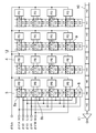
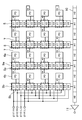
図15は、本発明の第1の実施形態に係る固体撮像装置の構成図である。ここでは、図面の簡略化のために、垂直方向に4画素分、水平方向に4画素分のみ示している。
図15は、本発明の第1の実施形態に係る固体撮像装置の構成図である。ここでは、図面の簡略化のために、垂直方向に4画素分、水平方向に4画素分のみ示している。
この固体撮像装置は、半導体基板に行列状に配置され、入射光を信号電荷に変換する複数の光電変換部(フォトダイオード)4と、光電変換部4に対応して設けられ、光電変換部4から読み出された信号電荷を列方向(垂直方向)に転送する垂直転送部5と、垂直転送部5によって転送された信号電荷を行方向(水平方向)に転送する水平転送部10と、水平転送部10によって転送された信号電荷を出力する電荷検出部11と、行毎に読み出すことが可能なように、光電変換部4のそれぞれに対応して設けられた第1の読み出し電極8a及び第2の読み出し電極8bとを備える。
ここで、固体撮像装置は、全画素読み出し(プログレッシブスキャン)対応のインターライントランスファー方式のCCDであり、例えば、垂直転送部5は、1画素あたり垂直転送電極8が4ゲートある4相駆動であり、水平転送部10は2相駆動である。光電変換部4からの信号電荷の読み出し電極は、4相駆動の垂直転送部5の、垂直転送電極8a及び8bが兼用した構成になっている。光電変換部4に溜まった信号電荷は、例えば、信号パケット9で表される電極に読み出され、転送される。
また、各画素には、全画素の信号電荷を掃き捨てるためのVOD12が備えられている。ただし、本発明の理解を容易とするため、VOD12は画素の面横方向に記載しているが、実際には画素のバルク方向(半導体基板の深さ方向)に構成されている。VOD12の基板に接続されているSub端子に高電圧が印加されると全画素の信号電荷は一括して基板に排出される構成となっている。
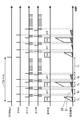
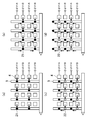
次に、図16及び図17(a)~図17(d)を用いて、図15の固体撮像装置の動作タイミングについて説明する。図16は、1フレーム期間内で、縦に隣接する2画素を垂直転送して加算する駆動タイミングの一例を示しており、図17(a)~図17(d)は、電荷加算及び電荷転送のイメージを示している。
まず、図16に示すように、垂直同期パルスVDは毎秒60フレーム(60fps)であり、各フレーム期間内に、赤外光照射下の信号電荷21と、背景光のみの場合の信号電荷22との双方の信号電荷が得られる。図16では、説明を簡単にするため、赤外光を照射した撮像と、背景光のみの撮像とを1フレームあたり2回ずつ行っている。
各フレームの初めに、基板排出パルス(φSub)を印加し、全画素の信号電荷を排出する。φSub印加終了により、1回目の赤外光照射露光期間Taが開始され、同時に赤外光が照射される。背景光は点灯継続しているため被写体からの反射光は、照射した赤外光と背景光との双方を含んでいる。
ここで、φV1Aに読み出しパルスを印加し、信号電荷21を垂直転送部5に読み出し、1回目の露光期間Taが終了する。同時に赤外光の照射も停止する。このときの光電変換部4から垂直転送部5への電荷読み出しのイメージは、図15にも光電変換部4からの矢印で示している。
なお、本実施形態では、赤外光照射期間と露光期間Taとを合致させているが、赤外光照射期間が背景光露光期間Tbを含まなければ、特に問題は生じない。
その後、図17(a)~図17(b)で示すように、読み出した信号電荷21を1画素分、隣接する画素まで順転送方向(図中下方)に転送させる。そして、φV1Bに読み出しパルスを印加し、垂直転送部5に信号電荷を読み出すが、その際、既にφV1Aから読み出していた信号電荷と加算する。加算した信号電荷21は、1画素分、先ほどと反対に、逆転送方向(図中上方)へ垂直転送する。
次に、φSubを印加し、全画素の信号電荷を排出したあと、図16の露光期間Tbで示すように、赤外光を照射せずに、赤外光源以外から発する赤外光成分、つまり背景光のみの信号電荷を光電変換部4に溜める。
そして、露光期間Tb終了時に、φV1Bに読み出しパルスを印加し、図17(c)に示すように、光電変換部4に溜まった背景光成分の信号電荷22を垂直転送部5に読み出す。その際、先ほどの照射赤外光を含む信号電荷21とは加算されないように、別パケットに読み出す。
その後、図17(d)に示すように、1画素分逆方向に垂直転送して、φV1Aに読み出しパルスを印加することで、隣接する縦2画素の信号を加算する。このときの加算する画素の組み合わせは、先ほどの信号電荷21を加算したときと同じ2画素である。
加算した後に、1画素分順方向に垂直転送して、信号電荷21及び信号電荷22を元の図17(a)と同じ位置に戻す。なお、図17(a)には、信号電荷22が示されていないが、図17(d)に示すように、信号電荷21に挟まれた空きパケットが信号電荷22の位置に相当する。
これら赤外光照射ON/OFFと図17(a)~図17(d)の一連の駆動とを1セットとして、図16に示す駆動タイミングでは、1フレーム期間内に2セット行ったあと、転送期間Tcで出力している。
以上、第1の実施形態に係る固体撮像装置によれば、垂直方向に隣り合う2つの画素から、赤外光を照射して得た信号電荷21と背景光のみの信号電荷22との2種類の信号を得ることが可能となり、2つの信号間での画素ずれが無くなる。これにより、2つの信号を使って背景光を減算した際に、同じアドレスから得た信号同士で減算するため、正確に距離画像を取得することが可能になる。しかも、画素部の設計が容易である。
更に、本実施形態の固体撮像装置であれば、全てのフォトダイオードに溜まった信号電荷を隣接加算することで利用するため、基板に掃き捨てる信号電荷が無くなり、利用率を100%にすることができる。また、感度が実質的に倍になることから、同じ赤外光の信号量が必要であるならば、照射する赤外光源の出力を下げる、あるいは、露光期間を短くすることも可能になる。つまり、低消費電力化に有効である。
また、1フレーム期間内で2回、赤外光を照射した信号電荷21と、背景光のみの信号電荷22とを読み出す駆動を繰り返すため、実質的に、2つの信号間の時間差が短くなり、動きの速い被写体を撮像して、2つの信号を使って背景光を減算したときにも、誤差が生じにくい。
なお、信号電荷の転送期間Tcにて出力される信号の並びは従来と同じであり、信号処理系は既存システムを使うことができるため、第1の実施形態の固体撮像装置は、従来の固体撮像装置から置き換えて、容易に取り扱うことができる。すなわち、既存システムとの親和性が高い。
これにより、赤外線照射も含めたシステム全体の電力と発熱とを抑えながら、より高精度なモーションセンサとして使用可能な固体撮像装置を実現できる。なお、1フレーム期間内の赤外光照射ON/OFFの繰り返しは、図17(a)~図17(d)では簡単のため2回となっているが、この回数が多ければ多いほど、動きの速い被写体には有効である。
また、これまで隣接2画素の加算駆動を中心に説明したが、加算せずに、一般的な駆動で全画素出力することで、距離画像でない、通常画像の撮像も可能である。
なお、第1の実施形態に係る固体撮像装置は、主にステレオ方式やパターン照射型の測距センサとして使われる。
《第2の実施形態》
以下、本発明の第2の実施形態に係る固体撮像装置について、第1の実施形態と異なる点を中心に説明する。第2の実施形態に係る固体撮像装置は、第1の実施形態に係る固体撮像装置と比較して、隣接する2つの画素から信号電荷を読み出す方法が異なり、更にそれに起因して、垂直転送部の構成が異なっている。しかし、垂直方向に隣り合う画素同士の信号電荷を加算することができる構造を提供することを目的とする点は、第1の実施形態に係る固体撮像装置と同様である。以下、第1の実施形態と異なる点を中心に説明し、同じ点は説明を省略する。
以下、本発明の第2の実施形態に係る固体撮像装置について、第1の実施形態と異なる点を中心に説明する。第2の実施形態に係る固体撮像装置は、第1の実施形態に係る固体撮像装置と比較して、隣接する2つの画素から信号電荷を読み出す方法が異なり、更にそれに起因して、垂直転送部の構成が異なっている。しかし、垂直方向に隣り合う画素同士の信号電荷を加算することができる構造を提供することを目的とする点は、第1の実施形態に係る固体撮像装置と同様である。以下、第1の実施形態と異なる点を中心に説明し、同じ点は説明を省略する。
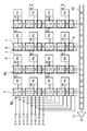
図18は、第2の実施形態に係る固体撮像装置の構成図である。この固体撮像装置は、第1の実施形態に係る図15の固体撮像装置と比較して、光電変換部4に対応して設けられた垂直転送部5へ、光電変換部4から信号電荷を読み出す電極が異なっており、第1の実施形態に係る図15の固体撮像装置に比べると、隣接する2画素の読み出し電極が近づいている。図15では、垂直転送電極中に4つおきに読み出し電極が配置されていたが、本実施形態に係る図18の固体撮像装置では、光電変換部4からの信号電荷の読み出し電極は、φV1及びφV3といったように、2電極離れたところに、2つの読み出し電極8a及び8bを配置した構成になっている。
次に、図19、図20(a)及び図20(b)を用いて、本実施形態に係る固体撮像装置の動作タイミングについて説明する。図19は、1フレーム期間内で、縦に隣接する2画素を加算する駆動タイミングの一例を示しており、第1の実施形態の図16と比較して、φV1及びφV3は同時に印加される点が異なる。
図20(a)及び図20(b)に示すように、赤外光を照射した露光期間の信号をφV1及びφV3に同時に読み出しパルスを印加することで、垂直転送部5に信号電荷21として読み出し、読み出すと同時に2画素の信号を1つの信号パケット中で加算する。この構成により、第1の実施形態と比較すると、2画素の信号を加算するために、1画素分垂直転送していた駆動が不要となる。このときの光電変換部4から垂直転送部5への電荷読み出しのイメージは、図18にも光電変換部4からの矢印で示している。
加算した信号電荷21は、1画素分、逆転送方向(図中上方)に垂直転送して、φSubで全画素の信号電荷を排出した後、露光期間Tbで溜めた信号電荷22を、先ほどと同じくφV1及びφV3に同時に読み出しパルスを印加することで、垂直転送部5の別パケットに読み出し、加算した信号電荷22が得られる。
その後、1画素分順方向に垂直転送して、信号電荷21及び信号電荷22を元の図20(a)と同じ位置に戻す。なお、図20(a)には、信号電荷22が示されていないが、図20(b)に示すように、信号電荷21に挟まれた空きパケットが信号電荷22の位置に相当する。
これら赤外光照射ON/OFFと図20(a)~図20(b)の一連の駆動とを1セットとして、図19に示す駆動タイミングでは、1フレーム期間内に2セット行ったあと、出力している。
以上、第2の実施形態に係る固体撮像装置によれば、隣接する2画素から読み出すタイミングが同時になることから、駆動タイミングの設計が容易になることに加えて、より正しく距離を計算することが可能となる。また、TOF型の測距センサ等、加算する2つの信号間で、時間差が生じると距離の誤判定に繋がる測距方式でも、使用することが可能になる。
また、出力される信号順については第1の実施形態で示されたものと同じであり、信号処理系は既存システムを使うことができるため、本実施形態の固体撮像装置も、第1の実施形態と同様に、従来の固体撮像装置から置き換えて、容易に取り扱うことができる。
更に、加算駆動をせずに、1フレームあたり1回読み出しの全画素出力(全画素独立読み出し)をしたい場合は、図18に示す、φV2をLOWレベルにしながらφV1及びφV3から同時に読み出すことで、各画素の光電変換部4に溜められた信号電荷を別パケットに読み出して、全画素出力することが可能である。これにより、1つのセンサから、駆動の違いだけで、距離画像の撮像も、通常画像の撮像もいずれも可能となる。
なお、図21(a)及び図21(b)に示すように、水平方向に隣接する2画素を加算することも有効である。この方法だと、水平方向に隣り合う2画素から、1つの共通した読み出し電極φV1A又はφV1Bを通じて読み出すだけで、垂直転送部5で加算することが可能となり、光電変換部4の端から読み出す必要のある、図18の固体撮像装置と比べると、光電変換部4から読み出しがしやすく、設計が容易であるとともに、より光電変換部4の中心近くに読み出し電極を配置することが可能のため、読み出し可能電圧も低く設定することができる。
《第3の実施形態》
以下、本発明の第3の実施形態に係る固体撮像装置について、第1の実施形態と異なる点を中心に説明する。第3の実施形態に係る固体撮像装置は、第1の実施形態に係る固体撮像装置と比較して、読み出し電極φV1A,φV1Bの配置が、列毎に1画素分ずれており、市松状になっている点が異なる。しかし、垂直方向に隣り合う画素同士の信号電荷を加算することができる構造を提供することを目的とする点は、第1の実施形態に係る固体撮像装置と同様である。以下、第1の実施形態と異なる点を中心に説明し、同じ点は説明を省略する。
以下、本発明の第3の実施形態に係る固体撮像装置について、第1の実施形態と異なる点を中心に説明する。第3の実施形態に係る固体撮像装置は、第1の実施形態に係る固体撮像装置と比較して、読み出し電極φV1A,φV1Bの配置が、列毎に1画素分ずれており、市松状になっている点が異なる。しかし、垂直方向に隣り合う画素同士の信号電荷を加算することができる構造を提供することを目的とする点は、第1の実施形態に係る固体撮像装置と同様である。以下、第1の実施形態と異なる点を中心に説明し、同じ点は説明を省略する。
図22は、第3の実施形態に係る固体撮像装置の構成図である。この固体撮像装置は、第1の実施形態に係る図15の固体撮像装置と比較して、光電変換部4に対応して設けられた垂直転送部5へ、光電変換部4から信号電荷を読み出す電極が異なっており、第1の実施形態に係る図15の固体撮像装置では、φV1Aの読み出し電極を有する画素の右隣の画素は同じくφV1Aの読み出し電極を有していたのに対し、第3の実施形態に係る図22の固体撮像装置では、φV1Aの読み出し電極を有する画素の右隣は、φV1Bの読み出し電極を有している画素が配置されている点が異なる。そして、そのφV1Bの読み出し電極を有する画素の右隣には、φV1Aの読み出し電極を有する画素が配置されている。一行下の画素は、その逆で、一番左の画素がφV1Bの読み出し電極を有していて、その右隣の画素は、φV1Aの読み出し電極を有している。このように、φV1Aの読み出し電極を有する画素とφV1Bの読み出し電極を有する画素とが、それぞれ市松状に配置されている。
次に、図23(a)~図23(d)を用いて、図22の固体撮像装置の動作タイミングについて説明する。なお、読み出し電極の配置が市松状になっている点が第1の実施形態と異なるだけで、駆動タイミング自体は、第1の実施形態に係る図16と同じである。
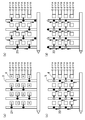
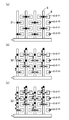
図23(a)~図23(d)に示すように、赤外光を照射した露光期間に得た信号電荷21と、赤外光を照射せずに背景光状態での露光期間に得た信号電荷22とは、市松状に信号が出力される。なお、図23(a)には、理解をしやすくするため、光電変換部4に、φV1Aで読み出す画素は「A」と記載し、φV1Bで読み出す画素は「B」と記載している。
その後は、第1の実施形態に係る図17(a)~図17(d)と同じ流れであり、図23(a)~図23(d)で示すように、赤外光を照射して得た信号電荷21を読み出して、次に、背景光のみで得た信号電荷22を読み出す。なお、図23(a)の時点での光電変換部4から垂直転送部5への電荷読み出しのイメージは、図22にも光電変換部4からの矢印で示している。
これら赤外光照射ON/OFFと図23(a)~図23(d)の一連の駆動とを1セットとして、第1の実施形態に係る、図16に示す駆動タイミングでは、1フレーム期間内に2セット行ったあと、転送期間Tcで出力している。
以上、第3の実施形態に係る固体撮像装置によれば、赤外光を照射して得た信号電荷から、赤外光を照射せずに得た信号電荷を減算することで、減算方向の解像度が半分に減っても、減算後の信号が市松化されていることにより、信号処理によってその解像度を補完することができるようになる。これにより、同じ画素数の従来の測距センサと比べても、より高精細な測距が可能になる。
なお、第1の実施形態と同様に、一般的な駆動で全画素読み出しすれば、通常の撮像も可能である。
《第4の実施形態》
以下、本発明の第4の実施形態に係る固体撮像装置について、第2の実施形態と異なる点を中心に説明する。第4の実施形態に係る固体撮像装置は、第2の実施形態に係る固体撮像装置と比較して、同時に加算する2画素の組み合わせが列毎に異なり、それに起因して、読み出し電極の構成が異なっている。しかし、垂直方向に隣り合う画素同士の信号電荷を加算することができる構造を提供することを目的とする点は、第2の実施形態に係る固体撮像装置と同様である。以下、第2の実施形態と異なる点を中心に説明し、同じ点は説明を省略する。
以下、本発明の第4の実施形態に係る固体撮像装置について、第2の実施形態と異なる点を中心に説明する。第4の実施形態に係る固体撮像装置は、第2の実施形態に係る固体撮像装置と比較して、同時に加算する2画素の組み合わせが列毎に異なり、それに起因して、読み出し電極の構成が異なっている。しかし、垂直方向に隣り合う画素同士の信号電荷を加算することができる構造を提供することを目的とする点は、第2の実施形態に係る固体撮像装置と同様である。以下、第2の実施形態と異なる点を中心に説明し、同じ点は説明を省略する。
図24は、第4の実施形態に係る固体撮像装置の構成図である。この固体撮像装置は、第2の実施形態に係る図18の固体撮像装置と比較して、光電変換部4に対応して設けられた垂直転送部5へ、光電変換部4から信号電荷を読み出す電極が列毎に異なっている。例えば、図18の固体撮像装置では、最も左下に配置された画素はφV3で読み出し、その右隣の画素もφV3で読み出していた。しかし、第4の実施形態に係る図24の固体撮像装置では、最も左下に配置された画素はφV3で読み出しているのに対し、その右隣の画素はφV1で読み出す構成になっている。更に、その右隣の画素は、φV3で読み出す構成になっている。
第4の実施形態に係る固体撮像装置は、第2の実施形態と比べて、読み出し電極の配置が列毎に異なるのみであるため、第4の実施形態に係る固体撮像装置の駆動タイミングは、第2の実施形態に係る駆動タイミングである図19に示す一例と同じである。
次に、図25(a)及び図25(b)を用いて、本実施形態に係る固体撮像装置の動作タイミングについて説明する。図25(a)及び図25(b)に示すように、赤外光を照射した露光期間に得た信号電荷21と、赤外光を照射せずに背景光状態での露光期間に得た信号電荷22とは、市松状に信号が出力される。なお、図25(a)には、理解をしやすくするため、光電変換部4に、φV1で読み出す画素は「1」と記載し、φV3で読み出す画素は「3」と記載している。
その後、第2の実施形態に係る図20(a)~図20(b)と同じように、図25(a)~図25(b)で示すように、赤外光を照射して得た信号電荷21を読み出して、次に、垂直転送した後、背景光のみで得た信号電荷22を読み出す。なお、図25(a)の時点での光電変換部4から垂直転送部5への電荷読み出しのイメージは、図24にも光電変換部4からの矢印で示している。
これら赤外光照射ON/OFFと図25(a)及び図25(b)の一連の駆動とを1セットとして、第2の実施形態に係る、図19に示す駆動タイミングでは、1フレーム期間内に2セット行ったあと、転送期間Tcで出力している。
以上、第4の実施形態に係る固体撮像装置によれば、赤外光を照射して得た信号電荷から、赤外光を照射せずに得た信号電荷を減算することで、減算方向の解像度が半分に減っても、減算後の信号が市松化されていることにより、信号処理によってその解像度を補完することができるようになる。これにより、同じ画素数の従来の測距センサと比べても、より高精細な測距が可能になる。
更に、第2の実施形態と同じく、隣接する2画素から読み出すタイミングが同時になることから、駆動タイミングの設計が容易になることに加えて、加算の同時性から特にTOF型の測距センサで有効である。例えば、光源パルスの立ち上がり部分で距離を算出する図10(a)及び図10(b)に示した第2のTOF法や、光源パルスの立ち下がり部分で距離を算出する図12(a)及び図12(b)に示した第3のTOF法も有効である。
なお、ここまで加算駆動を中心に説明したが、隣接2画素の加算駆動をせずに、1フレームあたり1回読み出しの全画素出力(全画素独立読み出し)をしたい場合は、第2の実施形態と同様に、φV2をLOWレベルにしながらφV1及びφV3から同時に読み出すことで、各画素の光電変換部4に溜められた信号電荷を別パケットに読み出して、全画素出力することが可能である。これにより、1つのセンサから、駆動の違いだけで、距離画像の撮像も、通常画像の撮像もいずれも可能となる。
《第5の実施形態》
以下、本発明の第5の実施形態に係る固体撮像装置について、第4の実施形態と異なる点を中心に説明する。第5の実施形態に係る固体撮像装置は、第4の実施形態に係る固体撮像装置と比較して、同時に加算する2画素の組み合わせが異なり、第5の実施形態では、横方向の2画素を加算しており、それに起因して、読み出し電極の構成が異なっている。しかし、隣り合う画素同士の信号電荷を加算することができる構造を提供することを目的とする点は、第4の実施形態に係る固体撮像装置と同様である。以下、第4の実施形態と異なる点を中心に説明し、同じ点は説明を省略する。
以下、本発明の第5の実施形態に係る固体撮像装置について、第4の実施形態と異なる点を中心に説明する。第5の実施形態に係る固体撮像装置は、第4の実施形態に係る固体撮像装置と比較して、同時に加算する2画素の組み合わせが異なり、第5の実施形態では、横方向の2画素を加算しており、それに起因して、読み出し電極の構成が異なっている。しかし、隣り合う画素同士の信号電荷を加算することができる構造を提供することを目的とする点は、第4の実施形態に係る固体撮像装置と同様である。以下、第4の実施形態と異なる点を中心に説明し、同じ点は説明を省略する。
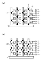
図26は、第5の実施形態に係る固体撮像装置の構成図である。この固体撮像装置は、第4の実施形態に係る図24の固体撮像装置と比較して、光電変換部4に対応して設けられた垂直転送部5へ、光電変換部4から信号電荷を読み出す電極が、垂直転送部5を挟んで水平方向に隣り合う光電変換部4のそれぞれから同時に読み出せる構造になっている。
なお、垂直転送電極φV1が全画素に配置されているため、垂直転送電極8の両側の画素から読み出してはいけない箇所と、垂直転送電極8aの両側の画素から読み出す箇所とが、図26に示すように市松状に存在する。このため、φV1のうち、信号電荷を読み出さない垂直転送電極8の両側にはチャネルストップ領域7を形成して、φV1に読み出しパルスを印加したときに、垂直転送部5に信号電荷が読み出されないようにする。また、逆に、φV1のうち、信号電荷を読み出す必要のある垂直転送電極8aの両側にはチャネルストップ領域7を設けずに、信号電荷を読み出しやすくする。なお、図が複雑になるため、例えば、第4の実施形態に係る固体撮像装置の構成図である図24に示されているφSubに関する記載は、図26では省いているが、第5の実施形態に係る固体撮像装置でも同様の構成である。
次に、図27及び図28(a)~図28(c)を用いて、本実施形態に係る固体撮像装置の動作タイミングについて説明する。図27は、1フレーム期間内で、横に隣接する2画素を同時に加算する駆動タイミングの一例を示しており、図28(a)~図28(c)は、電荷加算及び電荷転送のイメージを示している。
まず、図27に示すように、各フレーム期間内に、赤外光照射下の信号電荷21と、背景光のみの場合の信号電荷22との双方の信号電荷が得られるのは、第4の実施形態に係る固体撮像装置と変わりないが、φV1に読み出しパルスを印加するだけで、隣接する2画素を混合しながら読み出すことが可能である点が、第4の実施形態と異なる。
図27の露光期間Taで示すように、赤外光を照射して信号電荷を溜めて、φV1に読み出しパルスを印加し、図28(a)のように、市松状に信号電荷21を読み出して撮像する。このときの光電変換部4から垂直転送部5への電荷読み出しのイメージは、図26にも光電変換部4からの矢印で示している。その後、図28(b)で示すように、読み出した信号電荷21を1画素分、隣接する画素まで逆転送方向(図中上方)に転送させる。
次に、φSubを印加し、全画素の信号電荷を排出したあと、図27の露光期間Tbで示すように、赤外光を照射せずに、背景光のみの信号電荷を光電変換部4に溜める。そして、露光期間Tbの終了時に、φV1に読み出しパルスを印加し、図28(c)に示すように、市松状に信号電荷22を垂直転送部5に読み出す。その際、先ほどの照射赤外光を含む信号電荷21とは加算されないように、別パケットに読み出している。
その後、垂直転送部5に溜めた信号電荷を1画素分、先ほどとは逆に、順転送方向(図中下方)に1画素分転送し、再度、図27のTaで示す露光期間が開始する。これ以降は、図28(a)~図28(c)の流れと同じで、これを1セットとして、図27の駆動タイミングでは、赤外光照射ON/OFFと図28(a)~図28(c)の一連の駆動を2セット繰り返したあと、転送期間Tcで出力している。
以上、第5の実施形態に係る固体撮像装置によれば、水平方向に隣り合う2画素から、1つの共通した読み出し電極φV1を通じて読み出すだけで、垂直転送部5で加算することが可能となり、光電変換部4の端から読み出す必要のある、第4の実施形態に係る図24の固体撮像装置と比べると、光電変換部4の中心付近から読み出せるような電極構造にできるため、光電変換部4から信号電荷の読み出しがしやすく、設計が容易であるとともに、読み出し可能電圧も低く抑えることが可能である。
ここまで、加算駆動を中心に説明したが、隣接2画素の加算駆動をせずに、1フレームあたり1回読み出しの全画素出力(全画素独立読み出し)をしたい場合は、図26に示すように、読み出し電極を兼ねた垂直転送電極8bで表したφV2から読み出しができる設計にしておくことで、各画素の光電変換部4に溜められた信号電荷を別パケットに読み出して、全画素出力することが可能である。これにより、1つのセンサから、駆動の違いだけで、距離画像の撮像も、通常画像の撮像もいずれも可能となる。
別の実施形態として、図29に示すような固体撮像装置でもよい。図29の固体撮像装置は、図26に示す固体撮像装置と比較して、φV2の垂直転送電極が、全画素から読み出せる構成ではなく、市松状に読み出せるように配置されている。これにより、隣接2画素混合時の駆動は変わりないが、全画素読み出し時は、読み出し電極8bで示すφV2で光電変換部4bからまず信号パケット9bに電荷を読み出した後、φV1に読み出しパルスを印加して、光電変換部4aから信号パケット9aに電荷を読み出す。このとき、信号パケット9aには光電変換部4bからの電荷も読み出されるが、先ほどφV2で読み出したときから時間差が少なければ、光電変換部4bから読み出される信号量はごく微量であり、問題ない。図29の構成にすることで、光電変換部4から垂直転送部5に読み出す電極は、一方向あたり1電極だけであり、図26のような一方向あたり2電極あったものに比べて、読み出し部の設計がしやすい。
なお、隣接する2画素から読み出すタイミングが同時になることから、特にTOF型の測距センサで有効である。例えば、光源パルスの立ち上がり部分で距離を算出する図10(a)及び図10(b)に示した第2のTOF法や、光源パルスの立ち下がり部分で距離を算出する図12(a)及び図12(b)に示した第3のTOF法も有効である。
《第6の実施形態》
以下、本発明の第6の実施形態に係る固体撮像装置について、第5の実施形態と異なる点を中心に説明する。第6の実施形態に係る固体撮像装置は、第5の実施形態に係る固体撮像装置と比較して、垂直転送部の電極構成は同じであるがその駆動相数が異なり、それに起因して、垂直転送部に保持できる信号パケット数が異なっている。しかし、隣り合う画素同士の信号電荷を加算することができる構造を提供することを目的とする点は、第5の実施形態に係る固体撮像装置と同様である。以下、第5の実施形態と異なる点を中心に説明し、同じ点は説明を省略する。
以下、本発明の第6の実施形態に係る固体撮像装置について、第5の実施形態と異なる点を中心に説明する。第6の実施形態に係る固体撮像装置は、第5の実施形態に係る固体撮像装置と比較して、垂直転送部の電極構成は同じであるがその駆動相数が異なり、それに起因して、垂直転送部に保持できる信号パケット数が異なっている。しかし、隣り合う画素同士の信号電荷を加算することができる構造を提供することを目的とする点は、第5の実施形態に係る固体撮像装置と同様である。以下、第5の実施形態と異なる点を中心に説明し、同じ点は説明を省略する。
図30は、第6の実施形態に係る固体撮像装置の構成図である。この固体撮像装置は、第5の実施形態に係る図26の固体撮像装置と比較して、1画素4電極は変わらないが、垂直転送部5が8相駆動になっている。8相駆動になったことにより、第5の実施形態であれば、図26に示すように、1画素1パケット、つまり、2画素で2パケットのみ溜めることができたが、第6の実施形態に係る図30の構成であれば、2画素で3パケット溜めることが可能になる。
なお、溜められる信号パケットの数が増えたが、赤外光照射画像と背景光画像とを差分処理した際に生じる、画素ずれが生じないことは第5の実施形態と変わらない。また、解像度を上げられる点や、全画素の信号を利用することができる点も、第5の実施形態と同様である。
次に、図31及び図32(a)~図32(c)を用いて、本実施形態に係る固体撮像装置の動作タイミングについて説明する。図31は、1フレーム期間内で、横に隣接する2画素を同時に加算する駆動タイミングの一例を示しており、図32(a)~図32(c)は、電荷加算及び電荷転送のイメージを示している。
まず、図31に示すように、各フレーム期間内に、赤外光を照射して被写体からの反射光を含む信号電荷31と、先ほどとは異なるタイミングで赤外光を照射して被写体からの反射光を含む信号電荷32と、背景光のみを含む信号電荷33との3種類の信号電荷が得られる点が異なる。
図31の露光期間Taで示すように、赤外光を照射して信号電荷を溜めて、φV1及びφV5に読み出しパルスを印加し、図32(a)のように、市松状に信号電荷31を読み出す。このときの光電変換部4から垂直転送部5への電荷読み出しのイメージは、図30にも光電変換部4からの矢印で示している。その後、図32(b)で示すように、読み出した信号電荷31を、逆転送方向(図中上方)に転送させるが、これまでの実施形態と異なり、1画素分は転送させず、1~2電極分のみ転送させる。
次に、図31の露光期間Tbで示すように、露光期間Taとは異なるタイミングで赤外光を照射し、光電変換部4に溜まった電荷は、図32(b)で示すように、信号電荷31とは混合しないように、垂直転送部5に信号電荷32として読み出す。
更に、先ほどと同様に、2~3電極分信号を転送させて、図31の露光期間Tdで示すように、赤外光を照射せずに背景光による信号電荷だけを光電変換部4に溜めて、図32(c)に示すように、信号電荷31及び信号電荷32とは加算されないように、垂直転送部5の別パケットに信号電荷33として読み出す。
その後、垂直転送部5に溜めた信号電荷を1画素分、先ほどとは逆に順転送方向(図中下方)に1画素分転送し、また、図31のTaで示す露光期間が開始する。これ以降は、図32(a)~図32(c)の流れと同じで、これを1セットとすると、図31の駆動タイミングでは、赤外光照射のON/OFFや一連の駆動を2セット繰り返したあと、転送期間Tcで出力している。
第6の実施形態の固体撮像装置によれば、第5の実施形態の固体撮像装置と同じ構成の電極にも関わらず、駆動相数を変えるだけで、垂直転送部5に溜められる信号パケットの種類を増やすことが可能になる。駆動相数を変えるには、画素部の周辺に配置されているバスライン配線から垂直転送電極への接続の仕方を変えるだけで可能であり、画素部のレイアウトを変更する必要は無く、設計変更も容易である。
本実施形態の固体撮像装置は、3つの異なる信号電荷が溜められるので、図14(a)及び図14(b)に示した、背景光成分BGの除去を実行する第4のTOF法に適した固体撮像装置であって、測定距離精度の向上が可能となる。ただし、光源パルスの立ち上がり部分で距離を算出する図10(a)及び図10(b)に示した第2のTOF法や、光源パルスの立ち下がり部分で距離を算出する図12(a)及び図12(b)に示した第3のTOF法にも有効である。
また、第5の実施形態と同じく、φV2を用いることで全画素読み出しも可能である。これにより、1つのセンサから、駆動の違いだけで、距離画像の撮像も、通常画像の撮像もいずれも可能となる。
図30の実施形態の別の形態として、第5の実施形態の場合の図29のような、φV2から読み出す画素を市松状に配置して、読み出し部の設計をしやすくしてもよい。
以上、本発明の第1~第6の実施形態を説明したが、本発明は、これら実施形態に限定されるものではない。本発明の趣旨を逸脱しない限り、当業者が思いつく各種変形を本実施形態に施したものや、異なる実施形態における構成要素を組み合わせて構築される形態も、本発明の範囲内に含まれる。
例えば、上記の第1~第5の実施形態では、垂直転送部は4相駆動であった。しかし、3相駆動や5相駆動でも同じ効果を得ることが可能である。また、上記の第6の実施形態では、垂直転送部は8相駆動であったが、例えば10相駆動でも同じ効果を得ることが可能である。
上記第1~第6の実施形態に係る固体撮像装置を前述のステレオ方式、パターン照射型、又はTOF型の測距カメラに利用することにより、従来の固体撮像装置を使うときに比べて、感度や画素使用率が高いことで、赤外光照射パワーを下げたり、あるいは、露光時間を短くしたりすることができ、システム全体の低消費電力化が可能となる。
本発明は、高精度の距離画像を効率良く得ることができるので、特に測距カメラ等の撮像装置に利用することができる。
4,4a,4b 光電変換部
5 垂直転送部
7 画素分離部(チャネルストップ領域)
8 垂直転送電極
8a,8b 読み出し電極を兼ねる垂直転送電極
9,9a,9b 信号パケット
10 水平転送部
11 電荷検出部
12 縦型オーバーフロードレイン(VOD)
21 第1の信号電荷(赤外光+背景光)
22 第2の信号電荷(背景光)
31 第1の信号電荷(反射光1+背景光)
32 第2の信号電荷(反射光2+背景光)
33 第3の信号電荷(背景光)
100 撮影対象空間
101 被写体
102 背景光照明
103 赤外光源
104 レンズ
105 光学フィルタ
106 固体撮像装置
110,140 撮影対象空間
111,141,160 被写体
120,130,150,170 カメラ
121,131,151 レンズ
122,132,152 固体撮像装置
125,135,155,175 赤外光源
5 垂直転送部
7 画素分離部(チャネルストップ領域)
8 垂直転送電極
8a,8b 読み出し電極を兼ねる垂直転送電極
9,9a,9b 信号パケット
10 水平転送部
11 電荷検出部
12 縦型オーバーフロードレイン(VOD)
21 第1の信号電荷(赤外光+背景光)
22 第2の信号電荷(背景光)
31 第1の信号電荷(反射光1+背景光)
32 第2の信号電荷(反射光2+背景光)
33 第3の信号電荷(背景光)
100 撮影対象空間
101 被写体
102 背景光照明
103 赤外光源
104 レンズ
105 光学フィルタ
106 固体撮像装置
110,140 撮影対象空間
111,141,160 被写体
120,130,150,170 カメラ
121,131,151 レンズ
122,132,152 固体撮像装置
125,135,155,175 赤外光源
Claims (14)
- 被写体へ赤外光を照射する赤外光源と、
前記被写体からの入射光を受ける固体撮像装置とを備えた撮像装置であって、
前記固体撮像装置は、
基板上に行列状に配置された、入射光を信号電荷に変換する複数の第1の画素及び複数の第2の画素と、
前記第1及び第2の画素の信号電荷を同時に又は独立に、各画素に備えられた光電変換部から垂直転送部に排出する読み出し部とを備え、
前記垂直転送部は、1画素複数電極で構成され、1画素1信号溜める全画素読み出しが可能であり、かつ列方向の上下2方向どちらにも信号電荷を転送することが可能であり、
1フレーム走査期間内で、
第1の露光期間で、前記第1の画素から得た信号電荷と、前記第1の画素に隣接する前記第2の画素から得た信号電荷とを、前記垂直転送部上で加算して第1の信号電荷を作り、
第2の露光期間で、前記第1の画素から得た信号電荷と、前記第1の画素に隣接する前記第2の画素から得た信号電荷とを、前記垂直転送部上で、前記第1の信号電荷に加算しないように、前記垂直転送部を転送させて、別のパケットに第2の信号電荷として加算する駆動を、
複数回繰り返した後に出力することを特徴とする撮像装置。 - 前記第1の画素と前記第2の画素とは、行毎に交互に配置され、
垂直方向に隣接する前記第1の画素と前記第2の画素とを加算することを特徴とする請求項1記載の撮像装置。 - 前記第1の画素から信号電荷を読み出した後、垂直転送を1画素分行い、前記第2の画素から信号電荷を読み出すことで、前記第1の画素から読み出した信号電荷と加算することを特徴とする請求項2記載の撮像装置。
- 前記第1の画素と前記第2の画素との読み出し電極を1画素の間隔より近づけて配置することで、同時に1つのパケットに信号電荷を読み出すことを特徴とする請求項2記載の撮像装置。
- 被写体へ赤外光を照射する赤外光源と、
前記被写体からの入射光を受ける固体撮像装置とを備えた撮像装置であって、
前記固体撮像装置は、
基板上に行列状に配置された、入射光を信号電荷に変換する複数の第1の画素及び複数の第2の画素と、
前記第1及び第2の画素の信号電荷を同時に又は独立に、各画素に備えられた光電変換部から垂直転送部に排出する読み出し部とを備え、
前記垂直転送部は、1画素複数電極で構成され、1画素1信号溜める全画素読み出しが可能であり、かつ列方向の上下2方向どちらにも信号電荷を転送することが可能であり、
前記第1の画素と前記第2の画素とは、列毎に交互に配置され、
1フレーム走査期間内で、
第1の露光期間で、前記第1の画素から得た信号電荷と、前記第1の画素に水平方向に隣接する前記第2の画素から得た信号電荷とを、前記垂直転送部上で加算して第1の信号電荷を作り、
第2の露光期間で、前記第1の画素から得た信号電荷と、前記第1の画素に水平方向に隣接する別の第2の画素から得た信号電荷とを、別の垂直転送部上で、第2の信号電荷として加算する駆動を、
複数回繰り返した後に出力することを特徴とする撮像装置。 - 前記第1の画素と前記第2の画素とを、共通の読み出し電極で1つのパケットに同時に読み出すことを特徴とする請求項5記載の撮像装置。
- 前記第1の画素と前記第2の画素とを、それぞれ別の電極で1つのパケットに同時に読み出すことを特徴とする請求項5記載の撮像装置。
- 前記第1の画素と前記第2の画素とは、行毎に交互に配置され、また列毎にも交互に配置されることで、市松状となっていて、
垂直方向に隣接する前記第1の画素と前記第2の画素とを加算することを特徴とする請求項3又は4に記載の撮像装置。 - 前記第1の画素と前記第2の画素とは、列毎に交互に配置され、また行毎にも交互に配置されることで、市松状となっていて、
水平方向に隣接する前記第1の画素と前記第2の画素とを同時に読み出して加算することを特徴とする請求項1記載の撮像装置。 - 前記垂直転送部は、2画素複数電極で構成され、2画素で少なくとも3信号溜めることが可能であり、
1フレーム走査期間内で、前記第1の露光期間で得た第1の信号電荷と、前記第2の露光期間で得た第2の信号電荷とに加えて、第3の露光期間で、前記第1の画素から得た信号電荷と、前記第1の画素に隣接する前記第2の画素から得た信号電荷とを、前記垂直転送部上で加算して第3の信号電荷を作る駆動を繰り返すことを特徴とする請求項9記載の撮像装置。 - 前記第1の露光期間で、前記被写体を含む空間に前記赤外光を照射しながら撮像して、前記第1の信号電荷を作り、全画素の光電変換部に残る信号電荷を前記基板に掃き捨てた後、前記第2の露光期間で、前記赤外光を照射しない背景光のみの状態で撮像して、前記第2の信号電荷を作り、前記第1の信号電荷と前記第2の信号電荷との差分で背景光成分を除去して前記被写体までの距離を三角測量法により求めるステレオ方式の測距センサとして利用可能な請求項1~9のいずれか1項に記載の撮像装置。
- 前記第1の露光期間で、前記被写体を含む空間に前記赤外光を特定パターンで照射しながら撮像して、前記第1の信号電荷を作り、全画素の光電変換部に残る信号電荷を前記基板に掃き捨てた後、前記第2の露光期間で、前記赤外光を照射せずに撮像して、前記第2の信号電荷を作り、前記第1の信号電荷と前記第2の信号電荷との差分で背景光成分を除去して、各照射パターンの位置ずれ量によって前記被写体までの距離を求めるパターン照射型の測距センサとして利用可能な請求項1~9のいずれか1項に記載の撮像装置。
- 前記第1の露光期間で、前記赤外光をパルス状に発光させて前記被写体を含む空間に照射しながら、特定期間に受光される反射光を光電変換部から読み出して、前記第1の信号電荷を作り、また前記第2の露光期間で、別の特定期間に受光される反射光を光電変換部から読み出して、前記第2の信号電荷を作り、その比率で前記被写体までの距離を求めるTOF型の測距センサとして利用可能な請求項1~9のいずれか1項に記載の撮像装置。
- 前記第1の露光期間で、前記赤外光をパルス状に発光させて前記被写体に照射し、特定期間に受光される反射光を光電変換部から読み出して、前記第1の信号電荷を作り、また前記第2の露光期間で、別の特定期間に受光される反射光を光電変換部から読み出して、前記第2の信号電荷を作り、更に前記第3の露光期間で、別の特定期間に前記赤外光を照射せず撮像して背景光成分のみの第3の信号電荷を作り、その差分と比率で前記被写体までの距離を求めるTOF型の測距センサとして利用可能な請求項10記載の撮像装置。
Priority Applications (2)
| Application Number | Priority Date | Filing Date | Title |
|---|---|---|---|
| JP2014522405A JP6008148B2 (ja) | 2012-06-28 | 2013-06-12 | 撮像装置 |
| US14/565,224 US9787912B2 (en) | 2012-06-28 | 2014-12-09 | Image capture device |
Applications Claiming Priority (2)
| Application Number | Priority Date | Filing Date | Title |
|---|---|---|---|
| JP2012145385 | 2012-06-28 | ||
| JP2012-145385 | 2012-06-28 |
Related Child Applications (1)
| Application Number | Title | Priority Date | Filing Date |
|---|---|---|---|
| US14/565,224 Continuation US9787912B2 (en) | 2012-06-28 | 2014-12-09 | Image capture device |
Publications (1)
| Publication Number | Publication Date |
|---|---|
| WO2014002415A1 true WO2014002415A1 (ja) | 2014-01-03 |
Family
ID=49782615
Family Applications (1)
| Application Number | Title | Priority Date | Filing Date |
|---|---|---|---|
| PCT/JP2013/003693 Ceased WO2014002415A1 (ja) | 2012-06-28 | 2013-06-12 | 撮像装置 |
Country Status (3)
| Country | Link |
|---|---|
| US (1) | US9787912B2 (ja) |
| JP (1) | JP6008148B2 (ja) |
| WO (1) | WO2014002415A1 (ja) |
Cited By (18)
| Publication number | Priority date | Publication date | Assignee | Title |
|---|---|---|---|---|
| WO2015190015A1 (ja) * | 2014-06-09 | 2015-12-17 | パナソニックIpマネジメント株式会社 | 測距装置 |
| WO2016031171A1 (ja) * | 2014-08-29 | 2016-03-03 | パナソニックIpマネジメント株式会社 | 撮像装置 |
| CN106233089A (zh) * | 2014-02-08 | 2016-12-14 | 微软技术许可有限责任公司 | 针对立体匹配的环境依赖的主动照明 |
| JP2017133930A (ja) * | 2016-01-27 | 2017-08-03 | 倉敷紡績株式会社 | 距離画像生成装置および方法 |
| JPWO2016151982A1 (ja) * | 2015-03-26 | 2018-01-25 | パナソニックIpマネジメント株式会社 | 固体撮像素子およびこれを備えた撮像装置 |
| WO2018101049A1 (ja) * | 2016-11-29 | 2018-06-07 | パナソニックIpマネジメント株式会社 | 固体撮像装置及び測距撮像装置 |
| JP2019049480A (ja) * | 2017-09-11 | 2019-03-28 | 株式会社日立エルジーデータストレージ | 距離測定装置 |
| CN109791205A (zh) * | 2016-10-03 | 2019-05-21 | 齐诺马蒂赛股份有限公司 | 用于从成像阵列中的像素单元的曝光值减除背景光的方法以及用于该方法的像素单元 |
| JP2020056698A (ja) * | 2018-10-03 | 2020-04-09 | 株式会社日立エルジーデータストレージ | 測距撮像装置 |
| WO2020121705A1 (ja) * | 2018-12-14 | 2020-06-18 | パナソニックセミコンダクターソリューションズ株式会社 | 撮像装置 |
| JP2021085683A (ja) * | 2019-11-25 | 2021-06-03 | ファナック株式会社 | Tofセンサを用いた物体検出システム |
| JPWO2021182018A1 (ja) * | 2020-03-09 | 2021-09-16 | ||
| JP7137735B1 (ja) * | 2021-06-30 | 2022-09-14 | ヌヴォトンテクノロジージャパン株式会社 | 測距装置および測距方法 |
| WO2023276594A1 (ja) | 2021-06-30 | 2023-01-05 | ヌヴォトンテクノロジージャパン株式会社 | 測距装置および測距方法 |
| JP2023504157A (ja) * | 2019-12-01 | 2023-02-01 | マジック アイ インコーポレイテッド | 飛行時間情報を用いた三角測量ベースの3次元距離測定の向上 |
| WO2024004321A1 (ja) * | 2022-06-28 | 2024-01-04 | キヤノン株式会社 | 画像処理装置、頭部装着型表示装置、画像処理装置の制御方法、頭部装着型表示装置の制御方法、およびプログラム |
| WO2024062710A1 (ja) * | 2022-09-20 | 2024-03-28 | 株式会社Jvcケンウッド | 3次元映像撮像装置 |
| WO2024062706A1 (ja) * | 2022-09-20 | 2024-03-28 | 株式会社Jvcケンウッド | 3次元映像撮像装置 |
Families Citing this family (30)
| Publication number | Priority date | Publication date | Assignee | Title |
|---|---|---|---|---|
| US9819849B1 (en) * | 2016-07-01 | 2017-11-14 | Duelight Llc | Systems and methods for capturing digital images |
| JP6442710B2 (ja) * | 2013-07-23 | 2018-12-26 | パナソニックIpマネジメント株式会社 | 固体撮像装置、撮像装置及びその駆動方法 |
| WO2015033497A1 (ja) * | 2013-09-06 | 2015-03-12 | パナソニックIpマネジメント株式会社 | 撮像装置及びその駆動方法 |
| JP6303545B2 (ja) * | 2014-01-29 | 2018-04-04 | 株式会社リコー | 計測装置、投影装置、計測方法、及びプログラム |
| WO2015188146A2 (en) | 2014-06-05 | 2015-12-10 | Edward Hartley Sargent | Sensors and systems for the capture of scenes and events in space and time |
| US9692968B2 (en) | 2014-07-31 | 2017-06-27 | Invisage Technologies, Inc. | Multi-mode power-efficient light and gesture sensing in image sensors |
| US12401911B2 (en) | 2014-11-07 | 2025-08-26 | Duelight Llc | Systems and methods for generating a high-dynamic range (HDR) pixel stream |
| US12401912B2 (en) | 2014-11-17 | 2025-08-26 | Duelight Llc | System and method for generating a digital image |
| US12445736B2 (en) | 2015-05-01 | 2025-10-14 | Duelight Llc | Systems and methods for generating a digital image |
| KR102311688B1 (ko) | 2015-06-17 | 2021-10-12 | 엘지전자 주식회사 | 이동단말기 및 그 제어방법 |
| WO2017022218A1 (ja) * | 2015-08-04 | 2017-02-09 | パナソニックIpマネジメント株式会社 | 固体撮像装置 |
| EP3333893B1 (en) * | 2015-08-04 | 2020-02-19 | Panasonic Intellectual Property Management Co., Ltd. | Solid-state imaging device |
| US20190246053A1 (en) * | 2016-10-21 | 2019-08-08 | Invisage Technologies, Inc. | Motion tracking using multiple exposures |
| JP2018137569A (ja) * | 2017-02-21 | 2018-08-30 | ソニーセミコンダクタソリューションズ株式会社 | 測距装置、および測距方法 |
| WO2018230864A2 (ko) * | 2017-06-14 | 2018-12-20 | 엘지전자 주식회사 | 외부광을 반영하여 객체의 뎁스를 센싱하는 방법 및 이를 구현하는 장치 |
| CN119521033A (zh) | 2017-07-27 | 2025-02-25 | 麦克赛尔株式会社 | 摄像装置和便携终端 |
| CN111034177B (zh) * | 2017-09-14 | 2022-06-28 | 新唐科技日本株式会社 | 固体摄像装置以及具备该固体摄像装置的摄像装置 |
| CN107580185B (zh) * | 2017-09-30 | 2020-02-14 | 德淮半导体有限公司 | 图像传感器及操作方法以及成像装置 |
| CN108259744B (zh) * | 2018-01-24 | 2020-06-23 | 北京图森智途科技有限公司 | 图像采集控制方法及其装置、图像采集系统和tof相机 |
| CN112513671B (zh) * | 2018-08-02 | 2024-09-06 | 新唐科技日本株式会社 | 摄像装置、在该摄像装置中使用的固体摄像元件及摄像方法 |
| EP3640677B1 (en) * | 2018-10-17 | 2023-08-02 | Trimble Jena GmbH | Tracker of a surveying apparatus for tracking a target |
| JP7252755B2 (ja) * | 2018-12-27 | 2023-04-05 | 株式会社小糸製作所 | アクティブセンサ、物体識別システム、車両、車両用灯具 |
| WO2020166572A1 (ja) * | 2019-02-15 | 2020-08-20 | パナソニックセミコンダクターソリューションズ株式会社 | 撮像装置及び距離情報算出方法 |
| WO2020195046A1 (ja) * | 2019-03-27 | 2020-10-01 | パナソニックIpマネジメント株式会社 | 固体撮像装置 |
| US11763591B2 (en) | 2020-08-20 | 2023-09-19 | The Nielsen Company (Us), Llc | Methods and apparatus to determine an audience composition based on voice recognition, thermal imaging, and facial recognition |
| US11595723B2 (en) | 2020-08-20 | 2023-02-28 | The Nielsen Company (Us), Llc | Methods and apparatus to determine an audience composition based on voice recognition |
| US11553247B2 (en) * | 2020-08-20 | 2023-01-10 | The Nielsen Company (Us), Llc | Methods and apparatus to determine an audience composition based on thermal imaging and facial recognition |
| CN113298778B (zh) * | 2021-05-21 | 2023-04-07 | 奥比中光科技集团股份有限公司 | 一种基于飞行时间的深度计算方法、系统及存储介质 |
| US20230332890A1 (en) * | 2022-04-18 | 2023-10-19 | Analog Devices, Inc. | Quadrature trim vertical electrodes for yaw axis coriolis vibratory gyroscope |
| US12563312B2 (en) * | 2024-06-24 | 2026-02-24 | Stmicroelectronics International N.V. | Time-of-flight wake on attention |
Citations (4)
| Publication number | Priority date | Publication date | Assignee | Title |
|---|---|---|---|---|
| JP2003051987A (ja) * | 2001-08-06 | 2003-02-21 | Nippon Hoso Kyokai <Nhk> | 固体撮像装置及び固体撮像装置の駆動方法 |
| JP2007325026A (ja) * | 2006-06-01 | 2007-12-13 | Sharp Corp | 撮像装置、その駆動方法およびその信号処理方法、電子情報機器 |
| JP2008008700A (ja) * | 2006-06-28 | 2008-01-17 | Fujifilm Corp | 距離画像センサ |
| JP2011155702A (ja) * | 2011-05-02 | 2011-08-11 | Sony Corp | 固体撮像装置およびその駆動方法並びにカメラシステム |
Family Cites Families (27)
| Publication number | Priority date | Publication date | Assignee | Title |
|---|---|---|---|---|
| US7415126B2 (en) * | 1992-05-05 | 2008-08-19 | Automotive Technologies International Inc. | Occupant sensing system |
| US6906751B1 (en) * | 1998-07-22 | 2005-06-14 | Minolta Co., Ltd. | Digital camera and control method thereof |
| JP3009041B1 (ja) | 1999-02-16 | 2000-02-14 | 日本電気株式会社 | 固体撮像装置の駆動方法 |
| US7508421B2 (en) * | 2002-06-24 | 2009-03-24 | Fujifilm Corporation | Image pickup apparatus and image processing method |
| US7554587B2 (en) * | 2003-03-11 | 2009-06-30 | Fujifilm Corporation | Color solid-state image pickup device |
| US20040211444A1 (en) * | 2003-03-14 | 2004-10-28 | Taylor Charles E. | Robot vacuum with particulate detector |
| JP2005286115A (ja) * | 2004-03-30 | 2005-10-13 | Fuji Film Microdevices Co Ltd | 光電変換膜積層型固体撮像装置及びその駆動方法並びにデジタルカメラ |
| JP4533667B2 (ja) * | 2004-05-28 | 2010-09-01 | 富士フイルム株式会社 | 光電変換膜積層型固体撮像装置 |
| JP2006108379A (ja) * | 2004-10-05 | 2006-04-20 | Sony Corp | 固体撮像素子及びその駆動方法 |
| JP4625685B2 (ja) * | 2004-11-26 | 2011-02-02 | 株式会社東芝 | 固体撮像装置 |
| JP4247995B2 (ja) * | 2005-02-03 | 2009-04-02 | 富士通マイクロエレクトロニクス株式会社 | 固体撮像素子のデータ読出回路、撮像装置および固体撮像素子のデータ読出方法 |
| JP2009174854A (ja) | 2006-05-09 | 2009-08-06 | Panasonic Corp | 測距用画像選択機能を有する測距装置 |
| JP4544233B2 (ja) * | 2006-10-11 | 2010-09-15 | 株式会社デンソー | 車両検出装置及びヘッドランプ制御装置 |
| JP4843461B2 (ja) * | 2006-11-13 | 2011-12-21 | 株式会社東芝 | 固体撮像装置 |
| JP4887314B2 (ja) * | 2008-02-28 | 2012-02-29 | 富士フイルム株式会社 | 撮像装置及び画像信号処理方法 |
| JP5473951B2 (ja) * | 2009-02-13 | 2014-04-16 | パナソニック株式会社 | 固体撮像装置及びカメラ |
| US8681216B2 (en) * | 2009-03-12 | 2014-03-25 | Hewlett-Packard Development Company, L.P. | Depth-sensing camera system |
| DE102009031732B3 (de) * | 2009-07-04 | 2010-11-25 | Sick Ag | Entfernungsmessender optoelektronischer Sensor |
| KR101708682B1 (ko) * | 2010-03-03 | 2017-02-21 | 엘지전자 주식회사 | 영상표시장치 및 그 동작 방법. |
| US8446492B2 (en) * | 2009-12-10 | 2013-05-21 | Honda Motor Co., Ltd. | Image capturing device, method of searching for occlusion region, and program |
| CN103003945B (zh) * | 2010-06-18 | 2015-10-21 | 富士胶片株式会社 | 固态成像设备和数字照相机 |
| US20120056982A1 (en) * | 2010-09-08 | 2012-03-08 | Microsoft Corporation | Depth camera based on structured light and stereo vision |
| US9167138B2 (en) * | 2010-12-06 | 2015-10-20 | Apple Inc. | Pattern projection and imaging using lens arrays |
| EP2487504A1 (en) * | 2011-02-10 | 2012-08-15 | Technische Universität München | Method of enhanced depth image acquisition |
| JP5948837B2 (ja) * | 2011-03-29 | 2016-07-06 | ソニー株式会社 | 固体撮像素子及び電子機器 |
| US9142062B2 (en) * | 2011-03-29 | 2015-09-22 | Qualcomm Incorporated | Selective hand occlusion over virtual projections onto physical surfaces using skeletal tracking |
| US20160182846A1 (en) * | 2014-12-22 | 2016-06-23 | Google Inc. | Monolithically integrated rgb pixel array and z pixel array |
-
2013
- 2013-06-12 WO PCT/JP2013/003693 patent/WO2014002415A1/ja not_active Ceased
- 2013-06-12 JP JP2014522405A patent/JP6008148B2/ja active Active
-
2014
- 2014-12-09 US US14/565,224 patent/US9787912B2/en active Active
Patent Citations (4)
| Publication number | Priority date | Publication date | Assignee | Title |
|---|---|---|---|---|
| JP2003051987A (ja) * | 2001-08-06 | 2003-02-21 | Nippon Hoso Kyokai <Nhk> | 固体撮像装置及び固体撮像装置の駆動方法 |
| JP2007325026A (ja) * | 2006-06-01 | 2007-12-13 | Sharp Corp | 撮像装置、その駆動方法およびその信号処理方法、電子情報機器 |
| JP2008008700A (ja) * | 2006-06-28 | 2008-01-17 | Fujifilm Corp | 距離画像センサ |
| JP2011155702A (ja) * | 2011-05-02 | 2011-08-11 | Sony Corp | 固体撮像装置およびその駆動方法並びにカメラシステム |
Cited By (43)
| Publication number | Priority date | Publication date | Assignee | Title |
|---|---|---|---|---|
| US11265534B2 (en) | 2014-02-08 | 2022-03-01 | Microsoft Technology Licensing, Llc | Environment-dependent active illumination for stereo matching |
| CN106233089A (zh) * | 2014-02-08 | 2016-12-14 | 微软技术许可有限责任公司 | 针对立体匹配的环境依赖的主动照明 |
| CN106461763B (zh) * | 2014-06-09 | 2019-04-30 | 松下知识产权经营株式会社 | 测距装置以及该测距装置中使用的固体摄像元件 |
| CN106461763A (zh) * | 2014-06-09 | 2017-02-22 | 松下知识产权经营株式会社 | 测距装置 |
| WO2015190015A1 (ja) * | 2014-06-09 | 2015-12-17 | パナソニックIpマネジメント株式会社 | 測距装置 |
| JPWO2015190015A1 (ja) * | 2014-06-09 | 2017-04-20 | パナソニックIpマネジメント株式会社 | 測距装置、およびそれに用いられる固体撮像素子 |
| EP3188471A4 (en) * | 2014-08-29 | 2017-08-23 | Panasonic Intellectual Property Management Co., Ltd. | Imaging device |
| US10491842B2 (en) | 2014-08-29 | 2019-11-26 | Panasonic Intellectual Property Management Co., Ltd. | Imaging device, a solid-state imaging device for use in the imaging device |
| WO2016031171A1 (ja) * | 2014-08-29 | 2016-03-03 | パナソニックIpマネジメント株式会社 | 撮像装置 |
| JPWO2016031171A1 (ja) * | 2014-08-29 | 2017-07-20 | パナソニックIpマネジメント株式会社 | 撮像装置、及びそれに用いられる固体撮像装置 |
| CN106576146A (zh) * | 2014-08-29 | 2017-04-19 | 松下知识产权经营株式会社 | 摄像装置 |
| JPWO2016151982A1 (ja) * | 2015-03-26 | 2018-01-25 | パナソニックIpマネジメント株式会社 | 固体撮像素子およびこれを備えた撮像装置 |
| JP2017133930A (ja) * | 2016-01-27 | 2017-08-03 | 倉敷紡績株式会社 | 距離画像生成装置および方法 |
| CN109791205B (zh) * | 2016-10-03 | 2023-04-04 | 齐诺马蒂赛股份有限公司 | 用于从成像阵列中的像素单元的曝光值减除背景光的方法以及用于该方法的像素单元 |
| CN109791205A (zh) * | 2016-10-03 | 2019-05-21 | 齐诺马蒂赛股份有限公司 | 用于从成像阵列中的像素单元的曝光值减除背景光的方法以及用于该方法的像素单元 |
| US11276719B2 (en) | 2016-11-29 | 2022-03-15 | Nuvoton Technology Corporation Japan | Solid-state imaging device and distance-measuring imaging device |
| JPWO2018101049A1 (ja) * | 2016-11-29 | 2019-10-17 | パナソニックIpマネジメント株式会社 | 固体撮像装置及び測距撮像装置 |
| WO2018101049A1 (ja) * | 2016-11-29 | 2018-06-07 | パナソニックIpマネジメント株式会社 | 固体撮像装置及び測距撮像装置 |
| JP7018022B2 (ja) | 2016-11-29 | 2022-02-09 | ヌヴォトンテクノロジージャパン株式会社 | 固体撮像装置及び測距撮像装置 |
| JP2019049480A (ja) * | 2017-09-11 | 2019-03-28 | 株式会社日立エルジーデータストレージ | 距離測定装置 |
| JP7021885B2 (ja) | 2017-09-11 | 2022-02-17 | 株式会社日立エルジーデータストレージ | 距離測定装置 |
| JP2020056698A (ja) * | 2018-10-03 | 2020-04-09 | 株式会社日立エルジーデータストレージ | 測距撮像装置 |
| CN110988902A (zh) * | 2018-10-03 | 2020-04-10 | 日立乐金光科技株式会社 | 测距摄像装置 |
| JP7154924B2 (ja) | 2018-10-03 | 2022-10-18 | 株式会社日立エルジーデータストレージ | 測距撮像装置 |
| US11531102B2 (en) | 2018-10-03 | 2022-12-20 | Hitachi-Lg Data Storage, Inc. | Distance measurement image pickup apparatus |
| CN110988902B (zh) * | 2018-10-03 | 2023-05-12 | 日立乐金光科技株式会社 | 测距摄像装置 |
| US12265157B2 (en) | 2018-12-14 | 2025-04-01 | Miraxia Edge Technology Corporation | Imaging device |
| WO2020121705A1 (ja) * | 2018-12-14 | 2020-06-18 | パナソニックセミコンダクターソリューションズ株式会社 | 撮像装置 |
| JP2021085683A (ja) * | 2019-11-25 | 2021-06-03 | ファナック株式会社 | Tofセンサを用いた物体検出システム |
| JP7364439B2 (ja) | 2019-11-25 | 2023-10-18 | ファナック株式会社 | Tofセンサを用いた物体検出システム |
| JP7569376B2 (ja) | 2019-12-01 | 2024-10-17 | マジック アイ インコーポレイテッド | 飛行時間情報を用いた三角測量ベースの3次元距離測定の向上 |
| JP2023504157A (ja) * | 2019-12-01 | 2023-02-01 | マジック アイ インコーポレイテッド | 飛行時間情報を用いた三角測量ベースの3次元距離測定の向上 |
| JPWO2021182018A1 (ja) * | 2020-03-09 | 2021-09-16 | ||
| CN115052530A (zh) * | 2020-03-09 | 2022-09-13 | 松下知识产权经营株式会社 | 计测装置以及对计测装置进行控制的方法 |
| JP7617518B2 (ja) | 2020-03-09 | 2025-01-20 | パナソニックIpマネジメント株式会社 | 計測装置および計測装置を制御する方法 |
| WO2021182018A1 (ja) * | 2020-03-09 | 2021-09-16 | パナソニックIpマネジメント株式会社 | 計測装置および計測装置を制御する方法 |
| WO2023276594A1 (ja) | 2021-06-30 | 2023-01-05 | ヌヴォトンテクノロジージャパン株式会社 | 測距装置および測距方法 |
| JP7137735B1 (ja) * | 2021-06-30 | 2022-09-14 | ヌヴォトンテクノロジージャパン株式会社 | 測距装置および測距方法 |
| WO2024004321A1 (ja) * | 2022-06-28 | 2024-01-04 | キヤノン株式会社 | 画像処理装置、頭部装着型表示装置、画像処理装置の制御方法、頭部装着型表示装置の制御方法、およびプログラム |
| JP2024003912A (ja) * | 2022-06-28 | 2024-01-16 | キヤノン株式会社 | 画像処理装置、頭部装着型表示装置、画像処理装置の制御方法、頭部装着型表示装置の制御方法、およびプログラム |
| JP7555999B2 (ja) | 2022-06-28 | 2024-09-25 | キヤノン株式会社 | 画像処理装置、頭部装着型表示装置、画像処理装置の制御方法、頭部装着型表示装置の制御方法、およびプログラム |
| WO2024062710A1 (ja) * | 2022-09-20 | 2024-03-28 | 株式会社Jvcケンウッド | 3次元映像撮像装置 |
| WO2024062706A1 (ja) * | 2022-09-20 | 2024-03-28 | 株式会社Jvcケンウッド | 3次元映像撮像装置 |
Also Published As
| Publication number | Publication date |
|---|---|
| JP6008148B2 (ja) | 2016-10-19 |
| US20150092019A1 (en) | 2015-04-02 |
| JPWO2014002415A1 (ja) | 2016-05-30 |
| US9787912B2 (en) | 2017-10-10 |
Similar Documents
| Publication | Publication Date | Title |
|---|---|---|
| JP6008148B2 (ja) | 撮像装置 | |
| JP6442710B2 (ja) | 固体撮像装置、撮像装置及びその駆動方法 | |
| JP6145826B2 (ja) | 撮像装置及びその駆動方法 | |
| CN110024375B (zh) | 固态摄像装置和测距摄像装置 | |
| JP6374690B2 (ja) | 撮像装置及びその制御方法、プログラム、記憶媒体 | |
| US10491842B2 (en) | Imaging device, a solid-state imaging device for use in the imaging device | |
| JP5850680B2 (ja) | 撮像装置及びその制御方法 | |
| JP4600570B2 (ja) | 撮像装置 | |
| JP6583430B2 (ja) | 撮像装置および動き検出方法 | |
| JP6160971B2 (ja) | 固体撮像素子及び測距撮像装置 | |
| US9838611B2 (en) | Image capturing apparatus for obtaining normal image and range image and control method thereof | |
| JPWO2015033497A1 (ja) | 固体撮像装置、撮像装置及びその駆動方法 | |
| JP2016090785A (ja) | 撮像装置及びその制御方法 | |
| JP7426339B2 (ja) | 撮像装置、それに用いられる固体撮像素子及び撮像方法 | |
| JP2007158741A (ja) | 固体撮像装置 | |
| JP6700673B2 (ja) | 撮像装置、撮像システム | |
| WO2017073524A1 (ja) | 固体撮像素子 | |
| JP2007306482A (ja) | 撮像装置 | |
| JP2012227769A (ja) | 固体撮像素子の駆動方法 | |
| JPH04364680A (ja) | 撮像装置 | |
| JP2008236171A (ja) | 撮像素子およびそれを用いた撮像装置 | |
| JP2011151468A (ja) | テレビジョンカメラ |
Legal Events
| Date | Code | Title | Description |
|---|---|---|---|
| 121 | Ep: the epo has been informed by wipo that ep was designated in this application |
Ref document number: 13808504 Country of ref document: EP Kind code of ref document: A1 |
|
| ENP | Entry into the national phase |
Ref document number: 2014522405 Country of ref document: JP Kind code of ref document: A |
|
| NENP | Non-entry into the national phase |
Ref country code: DE |
|
| 122 | Ep: pct application non-entry in european phase |
Ref document number: 13808504 Country of ref document: EP Kind code of ref document: A1 |