WO2013180276A1 - 画像表示媒体の駆動装置、画像表示装置、駆動プログラム、及びコンピュータ読み取り媒体 - Google Patents
画像表示媒体の駆動装置、画像表示装置、駆動プログラム、及びコンピュータ読み取り媒体 Download PDFInfo
- Publication number
- WO2013180276A1 WO2013180276A1 PCT/JP2013/065212 JP2013065212W WO2013180276A1 WO 2013180276 A1 WO2013180276 A1 WO 2013180276A1 JP 2013065212 W JP2013065212 W JP 2013065212W WO 2013180276 A1 WO2013180276 A1 WO 2013180276A1
- Authority
- WO
- WIPO (PCT)
- Prior art keywords
- particles
- substrate
- voltage
- particle
- image display
- Prior art date
Links
Images


Classifications
-
- G—PHYSICS
- G09—EDUCATION; CRYPTOGRAPHY; DISPLAY; ADVERTISING; SEALS
- G09G—ARRANGEMENTS OR CIRCUITS FOR CONTROL OF INDICATING DEVICES USING STATIC MEANS TO PRESENT VARIABLE INFORMATION
- G09G3/00—Control arrangements or circuits, of interest only in connection with visual indicators other than cathode-ray tubes
- G09G3/20—Control arrangements or circuits, of interest only in connection with visual indicators other than cathode-ray tubes for presentation of an assembly of a number of characters, e.g. a page, by composing the assembly by combination of individual elements arranged in a matrix no fixed position being assigned to or needed to be assigned to the individual characters or partial characters
- G09G3/34—Control arrangements or circuits, of interest only in connection with visual indicators other than cathode-ray tubes for presentation of an assembly of a number of characters, e.g. a page, by composing the assembly by combination of individual elements arranged in a matrix no fixed position being assigned to or needed to be assigned to the individual characters or partial characters by control of light from an independent source
- G09G3/3433—Control arrangements or circuits, of interest only in connection with visual indicators other than cathode-ray tubes for presentation of an assembly of a number of characters, e.g. a page, by composing the assembly by combination of individual elements arranged in a matrix no fixed position being assigned to or needed to be assigned to the individual characters or partial characters by control of light from an independent source using light modulating elements actuated by an electric field and being other than liquid crystal devices and electrochromic devices
- G09G3/344—Control arrangements or circuits, of interest only in connection with visual indicators other than cathode-ray tubes for presentation of an assembly of a number of characters, e.g. a page, by composing the assembly by combination of individual elements arranged in a matrix no fixed position being assigned to or needed to be assigned to the individual characters or partial characters by control of light from an independent source using light modulating elements actuated by an electric field and being other than liquid crystal devices and electrochromic devices based on particles moving in a fluid or in a gas, e.g. electrophoretic devices
-
- G—PHYSICS
- G02—OPTICS
- G02F—OPTICAL DEVICES OR ARRANGEMENTS FOR THE CONTROL OF LIGHT BY MODIFICATION OF THE OPTICAL PROPERTIES OF THE MEDIA OF THE ELEMENTS INVOLVED THEREIN; NON-LINEAR OPTICS; FREQUENCY-CHANGING OF LIGHT; OPTICAL LOGIC ELEMENTS; OPTICAL ANALOGUE/DIGITAL CONVERTERS
- G02F1/00—Devices or arrangements for the control of the intensity, colour, phase, polarisation or direction of light arriving from an independent light source, e.g. switching, gating or modulating; Non-linear optics
- G02F1/01—Devices or arrangements for the control of the intensity, colour, phase, polarisation or direction of light arriving from an independent light source, e.g. switching, gating or modulating; Non-linear optics for the control of the intensity, phase, polarisation or colour
- G02F1/0121—Operation of devices; Circuit arrangements, not otherwise provided for in this subclass
-
- G—PHYSICS
- G02—OPTICS
- G02F—OPTICAL DEVICES OR ARRANGEMENTS FOR THE CONTROL OF LIGHT BY MODIFICATION OF THE OPTICAL PROPERTIES OF THE MEDIA OF THE ELEMENTS INVOLVED THEREIN; NON-LINEAR OPTICS; FREQUENCY-CHANGING OF LIGHT; OPTICAL LOGIC ELEMENTS; OPTICAL ANALOGUE/DIGITAL CONVERTERS
- G02F1/00—Devices or arrangements for the control of the intensity, colour, phase, polarisation or direction of light arriving from an independent light source, e.g. switching, gating or modulating; Non-linear optics
- G02F1/01—Devices or arrangements for the control of the intensity, colour, phase, polarisation or direction of light arriving from an independent light source, e.g. switching, gating or modulating; Non-linear optics for the control of the intensity, phase, polarisation or colour
- G02F1/165—Devices or arrangements for the control of the intensity, colour, phase, polarisation or direction of light arriving from an independent light source, e.g. switching, gating or modulating; Non-linear optics for the control of the intensity, phase, polarisation or colour based on translational movement of particles in a fluid under the influence of an applied field
- G02F1/166—Devices or arrangements for the control of the intensity, colour, phase, polarisation or direction of light arriving from an independent light source, e.g. switching, gating or modulating; Non-linear optics for the control of the intensity, phase, polarisation or colour based on translational movement of particles in a fluid under the influence of an applied field characterised by the electro-optical or magneto-optical effect
- G02F1/167—Devices or arrangements for the control of the intensity, colour, phase, polarisation or direction of light arriving from an independent light source, e.g. switching, gating or modulating; Non-linear optics for the control of the intensity, phase, polarisation or colour based on translational movement of particles in a fluid under the influence of an applied field characterised by the electro-optical or magneto-optical effect by electrophoresis
-
- G—PHYSICS
- G02—OPTICS
- G02F—OPTICAL DEVICES OR ARRANGEMENTS FOR THE CONTROL OF LIGHT BY MODIFICATION OF THE OPTICAL PROPERTIES OF THE MEDIA OF THE ELEMENTS INVOLVED THEREIN; NON-LINEAR OPTICS; FREQUENCY-CHANGING OF LIGHT; OPTICAL LOGIC ELEMENTS; OPTICAL ANALOGUE/DIGITAL CONVERTERS
- G02F1/00—Devices or arrangements for the control of the intensity, colour, phase, polarisation or direction of light arriving from an independent light source, e.g. switching, gating or modulating; Non-linear optics
- G02F1/01—Devices or arrangements for the control of the intensity, colour, phase, polarisation or direction of light arriving from an independent light source, e.g. switching, gating or modulating; Non-linear optics for the control of the intensity, phase, polarisation or colour
- G02F1/165—Devices or arrangements for the control of the intensity, colour, phase, polarisation or direction of light arriving from an independent light source, e.g. switching, gating or modulating; Non-linear optics for the control of the intensity, phase, polarisation or colour based on translational movement of particles in a fluid under the influence of an applied field
- G02F1/1685—Operation of cells; Circuit arrangements affecting the entire cell
-
- G—PHYSICS
- G09—EDUCATION; CRYPTOGRAPHY; DISPLAY; ADVERTISING; SEALS
- G09G—ARRANGEMENTS OR CIRCUITS FOR CONTROL OF INDICATING DEVICES USING STATIC MEANS TO PRESENT VARIABLE INFORMATION
- G09G3/00—Control arrangements or circuits, of interest only in connection with visual indicators other than cathode-ray tubes
- G09G3/20—Control arrangements or circuits, of interest only in connection with visual indicators other than cathode-ray tubes for presentation of an assembly of a number of characters, e.g. a page, by composing the assembly by combination of individual elements arranged in a matrix no fixed position being assigned to or needed to be assigned to the individual characters or partial characters
- G09G3/2003—Display of colours
-
- G—PHYSICS
- G09—EDUCATION; CRYPTOGRAPHY; DISPLAY; ADVERTISING; SEALS
- G09G—ARRANGEMENTS OR CIRCUITS FOR CONTROL OF INDICATING DEVICES USING STATIC MEANS TO PRESENT VARIABLE INFORMATION
- G09G3/00—Control arrangements or circuits, of interest only in connection with visual indicators other than cathode-ray tubes
- G09G3/20—Control arrangements or circuits, of interest only in connection with visual indicators other than cathode-ray tubes for presentation of an assembly of a number of characters, e.g. a page, by composing the assembly by combination of individual elements arranged in a matrix no fixed position being assigned to or needed to be assigned to the individual characters or partial characters
- G09G3/2007—Display of intermediate tones
- G09G3/2014—Display of intermediate tones by modulation of the duration of a single pulse during which the logic level remains constant
-
- G—PHYSICS
- G02—OPTICS
- G02F—OPTICAL DEVICES OR ARRANGEMENTS FOR THE CONTROL OF LIGHT BY MODIFICATION OF THE OPTICAL PROPERTIES OF THE MEDIA OF THE ELEMENTS INVOLVED THEREIN; NON-LINEAR OPTICS; FREQUENCY-CHANGING OF LIGHT; OPTICAL LOGIC ELEMENTS; OPTICAL ANALOGUE/DIGITAL CONVERTERS
- G02F1/00—Devices or arrangements for the control of the intensity, colour, phase, polarisation or direction of light arriving from an independent light source, e.g. switching, gating or modulating; Non-linear optics
- G02F1/01—Devices or arrangements for the control of the intensity, colour, phase, polarisation or direction of light arriving from an independent light source, e.g. switching, gating or modulating; Non-linear optics for the control of the intensity, phase, polarisation or colour
- G02F1/23—Devices or arrangements for the control of the intensity, colour, phase, polarisation or direction of light arriving from an independent light source, e.g. switching, gating or modulating; Non-linear optics for the control of the intensity, phase, polarisation or colour for the control of the colour
-
- G—PHYSICS
- G09—EDUCATION; CRYPTOGRAPHY; DISPLAY; ADVERTISING; SEALS
- G09G—ARRANGEMENTS OR CIRCUITS FOR CONTROL OF INDICATING DEVICES USING STATIC MEANS TO PRESENT VARIABLE INFORMATION
- G09G2310/00—Command of the display device
- G09G2310/02—Addressing, scanning or driving the display screen or processing steps related thereto
- G09G2310/0264—Details of driving circuits
- G09G2310/0289—Details of voltage level shifters arranged for use in a driving circuit
-
- G—PHYSICS
- G09—EDUCATION; CRYPTOGRAPHY; DISPLAY; ADVERTISING; SEALS
- G09G—ARRANGEMENTS OR CIRCUITS FOR CONTROL OF INDICATING DEVICES USING STATIC MEANS TO PRESENT VARIABLE INFORMATION
- G09G2310/00—Command of the display device
- G09G2310/06—Details of flat display driving waveforms
-
- G—PHYSICS
- G09—EDUCATION; CRYPTOGRAPHY; DISPLAY; ADVERTISING; SEALS
- G09G—ARRANGEMENTS OR CIRCUITS FOR CONTROL OF INDICATING DEVICES USING STATIC MEANS TO PRESENT VARIABLE INFORMATION
- G09G2310/00—Command of the display device
- G09G2310/06—Details of flat display driving waveforms
- G09G2310/068—Application of pulses of alternating polarity prior to the drive pulse in electrophoretic displays
-
- G—PHYSICS
- G09—EDUCATION; CRYPTOGRAPHY; DISPLAY; ADVERTISING; SEALS
- G09G—ARRANGEMENTS OR CIRCUITS FOR CONTROL OF INDICATING DEVICES USING STATIC MEANS TO PRESENT VARIABLE INFORMATION
- G09G2310/00—Command of the display device
- G09G2310/08—Details of timing specific for flat panels, other than clock recovery
-
- G—PHYSICS
- G09—EDUCATION; CRYPTOGRAPHY; DISPLAY; ADVERTISING; SEALS
- G09G—ARRANGEMENTS OR CIRCUITS FOR CONTROL OF INDICATING DEVICES USING STATIC MEANS TO PRESENT VARIABLE INFORMATION
- G09G2320/00—Control of display operating conditions
- G09G2320/02—Improving the quality of display appearance
- G09G2320/0242—Compensation of deficiencies in the appearance of colours
-
- G—PHYSICS
- G09—EDUCATION; CRYPTOGRAPHY; DISPLAY; ADVERTISING; SEALS
- G09G—ARRANGEMENTS OR CIRCUITS FOR CONTROL OF INDICATING DEVICES USING STATIC MEANS TO PRESENT VARIABLE INFORMATION
- G09G2320/00—Control of display operating conditions
- G09G2320/02—Improving the quality of display appearance
- G09G2320/0252—Improving the response speed
-
- G—PHYSICS
- G09—EDUCATION; CRYPTOGRAPHY; DISPLAY; ADVERTISING; SEALS
- G09G—ARRANGEMENTS OR CIRCUITS FOR CONTROL OF INDICATING DEVICES USING STATIC MEANS TO PRESENT VARIABLE INFORMATION
- G09G2320/00—Control of display operating conditions
- G09G2320/04—Maintaining the quality of display appearance
-
- G—PHYSICS
- G09—EDUCATION; CRYPTOGRAPHY; DISPLAY; ADVERTISING; SEALS
- G09G—ARRANGEMENTS OR CIRCUITS FOR CONTROL OF INDICATING DEVICES USING STATIC MEANS TO PRESENT VARIABLE INFORMATION
- G09G3/00—Control arrangements or circuits, of interest only in connection with visual indicators other than cathode-ray tubes
- G09G3/20—Control arrangements or circuits, of interest only in connection with visual indicators other than cathode-ray tubes for presentation of an assembly of a number of characters, e.g. a page, by composing the assembly by combination of individual elements arranged in a matrix no fixed position being assigned to or needed to be assigned to the individual characters or partial characters
- G09G3/2007—Display of intermediate tones
Definitions
- the present invention relates to an image display medium driving apparatus, an image display apparatus, a driving program, and a computer reading medium.
- an image display medium using colored particles is known as an image display medium that has memory characteristics and can be rewritten repeatedly.
- Such an image display medium includes, for example, a pair of substrates and a plurality of types of particle groups that are sealed between the substrates so as to be movable between the substrates by an applied electric field and have different colors and charging characteristics. Is done.
- a voltage corresponding to an image is applied between a pair of substrates to move the particles and display an image as a contrast between particles of different colors. Further, the image display is maintained even after the voltage application is stopped after the image is displayed.
- Patent Document 1 includes a display medium including a black colored dispersion medium, and colored electrophoretic particles dispersed in the dispersion medium, colored in different colors, and having different electrophoretic mobility, There has been disclosed a display device in which different colors are displayed by applying different electric fields such as intensity, direction, and application time to a display medium.
- Patent Document 2 encloses a plurality of types of particle groups having different adhesion forces to the display substrate and the back substrate, that is, electric field strength for starting movement, in a dispersion medium between the display substrate and the back substrate.
- the desired particles are selectively moved so that particles of colors other than the desired color move in the dispersion medium. It is disclosed that the movement is suppressed to suppress a color mixture in which colors other than a desired color are mixed.
- An object of the present invention is to improve the controllability of particles as compared with the case of driving particles by controlling the magnitude of voltage.
- At least one is sealed between a pair of light-transmitting substrates, and a plurality of times at which the separation starts from a state of being attached to the substrate when a predetermined voltage is applied are different.
- the voltage application unit that applies the voltage between the pair of substrates of the image display medium having the kind of particles, and the voltage so that the time for applying the voltage between the pair of substrates can be varied according to image information.
- a control unit that controls the application unit.
- At least one is sealed between a pair of translucent substrates, is colored in a different color for each type, and maintains a state of being attached to the substrate.
- a voltage applying unit that applies a voltage between the pair of substrates of the display medium, and a voltage with a magnitude that separates the substrate from a state in which the particles having the largest adhesion force among the plurality of types of particles adhere to one substrate.
- An image display comprising: a control unit that controls the voltage application unit so that the voltage is applied between the pair of substrates based on the image information in an application time corresponding to the adhesion force of particles to be detached from the substrate.
- Medium is a dynamic system.
- the control unit has a size such that the particles having the largest adhesion force among the plurality of types of particles are detached from the substrate, and at least a part of the particles to be separated from the substrate as the application time is detached from the substrate.
- the control unit is configured such that, among the plurality of types of particles, the particles having the largest adhesion force are separated from the substrate, and at least a part of the particles having the largest adhesion force as the application time is from the substrate.
- At least one of the substrates is sealed between a pair of translucent substrates and has charging characteristics, and is detached from the adhered substrate by a voltage applied between the substrates.
- a voltage applying unit that applies a voltage between the pair of substrates of an image display medium that includes particles and displays an image based on image information; and the particles are detached from the substrate from a state where the particles are attached to the substrate.
- Control for controlling the voltage application unit so that a voltage having a magnitude larger than the adhesive force required for the separation and a time during which at least a part of the particles are detached from the substrate is applied between the substrates based on the image information.
- an image display medium driving device for controlling the voltage application unit so that a voltage having a magnitude larger than the adhesive force required for the separation and a time during which at least a part of the particles are detached from the substrate is applied between the substrates based on the image information.
- Each of the plurality of types of particles has a detachment time distribution from when the particles start to detach from the substrate until all particles detach from the substrate, and detaches from the substrate according to the detachment time distribution ( The image display medium drive device according to any one of 1) to (5).
- the disengagement time distribution of each of the plurality of types of particles has a predetermined A% (A> 50) of particles having a shorter time to start disengagement from the substrate after application of the voltage is started.
- the particle having a shorter time to start detachment from the substrate has a larger particle size ⁇ charge density than the particle having a longer time to start detaching from the substrate (6 Or (7).
- an image display device including the image display medium and the image display medium driving device according to (1).
- an image display device including the image display medium and the image display medium driving device according to any one of (2) to (4). .
- an image display device including the image display medium and the image display medium driving device according to (5).
- a drive program for causing a computer to function as the control unit of the drive device for an image display medium according to any one of (1) to (8) is stored.
- an image display medium driving device capable of improving the controllability of particles as compared with the case of driving particles by controlling the magnitude of voltage.
- a plurality of types of particles can be selectively driven.
- a driving program that can shorten the image rewriting time as compared with the case of driving particles by controlling the magnitude of the voltage.
- a non-transitory computer-readable medium that stores a driving program capable of shortening an image rewriting time compared to driving particles by controlling the magnitude of voltage. Can be provided.
- FIG. It is the schematic of the image display apparatus concerning this embodiment. It is a block diagram which shows the structure of the control part of the image display apparatus concerning this embodiment. It is a figure which shows an example of the operation
- FIG. It is a figure which shows an example of the relationship between the response time when the particle
- FIG. 7A An example in which 80% of particles in the particle group (particle A) with a short separation start time T80A ⁇ time T20B in which 20% of the particles in the particle group (particle B) with a long separation start time (particle B) is separated
- FIG. 7A An example in which 95% of the particles in the particle group (particle A) with a short start time (particle A) T95A ⁇ the time T5B in which 5% of the particles in the particle group (particle B) with a long start time (particle B) leave is shown.
- FIG. It is a figure which shows an example of the pulse application time in case the separation time distribution of each particle group is not completely separated. It is a schematic diagram which shows the movement of the particle
- FIG. 7C It is a figure which shows the other example of the pulse application time in case the separation time distribution of each particle group is not isolate
- FIG. 11A It is a figure which shows the example of a change of the display density with respect to the application time of the drive pulse of FIG. 11A. It is a figure which shows the relationship between the voltage of particle
- FIG. 13A is a diagram showing an example of change in display density with respect to the application time of the drive pulse in FIG. 13A. It is a figure which shows the relationship between the voltage of particle
- the adhesion force of the present invention means a force necessary to maintain a state where particles are adhered to the substrate.
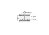
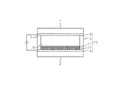
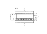
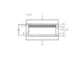
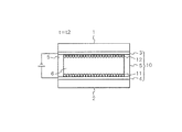
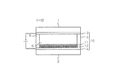
- FIG. 1A schematically shows an image display apparatus according to the present embodiment.
- the image display device 100 includes an image display medium 10 and a drive device 20 that drives the image display medium 10.
- the driving device 20 includes a voltage application unit 30 that applies a voltage between the display-side electrode 3 and the back-side electrode 4 of the image display medium 10, and a voltage application unit 30 according to image information of an image displayed on the image display medium 10. And a control unit 40 to be controlled.
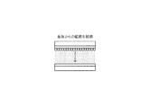
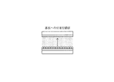
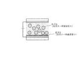
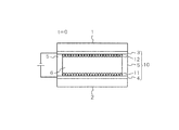
- the image display medium 10 includes a pair of substrates in which a translucent display substrate 1 serving as an image display surface and a rear substrate 2 serving as a non-display surface are disposed to face each other with a gap therebetween. .
- a gap member 5 is provided that holds the substrates 1 and 2 at a predetermined interval and partitions the substrates into a plurality of cells.
- the cell indicates a region surrounded by the back substrate 2 provided with the back side electrode 4, the display substrate 1 provided with the display side electrode 3, and the gap member 5.
- a dispersion medium 6 made of an insulating liquid, a first particle group 11 and a second particle group 12 dispersed in the dispersion medium 6 are enclosed.
- the first particle group 11 is a particle group of particle A described later
- the second particle group 12 is a particle group of particle B described later.
- the first particle group 11 and the second particle group 12 are colored in different colors. Further, the adhesion forces for maintaining the state of being attached to the substrate are different from each other, and the voltages necessary for releasing the substrate from the state of being attached to the substrate by the electric field between the substrates are different from each other. Then, by controlling the voltage applied between the pair of electrodes 3 and 4, the first particle group 11 and the second particle group 12 have a characteristic of migrating independently. More specifically, when the force in the direction in which the particles leave the substrate exceeds the adhesion force by the electric field generated by applying a voltage, the particles leave the substrate and go to the other substrate. The voltage at which the force generated by the electric field is balanced with the adhesive force and the particles start to move is called a threshold voltage.
- the particles are caused by van der Waals force, mirror image force, electrostatic attractive force, or the like. It remains attached to the substrate and the image display is maintained.
- the adhesion force of the particles it is only necessary to adjust the mirror image force, electrostatic attraction force, van der Waals force, and the like.
- the charge amount of the particles, the particle size, the charge density, the dielectric constant, The surface shape, the surface energy, the composition and density of the dispersing agent, etc. can be appropriately adjusted.
- a white particle group colored in white may be included.
- the white particle group has a smaller amount of charge than the first particle group 11 and the second particle group 12, and the voltage at which the first particle group 11 and the second particle group 12 move to one of the electrode sides is the electrode. Even if it is applied in between, it may be a floating particle group that does not move to any electrode side. Or you may make it comprise with two types of particle groups, the 1st particle group 11 or the 2nd particle group 12, and a floating particle group. Or it is good also as a structure which displays the color (for example, white) different from the color of electrophoretic particle by mixing a coloring agent with a dispersion medium.
- the driving device 20 controls the voltage applied between the display-side electrode 3 and the back-side electrode 4 of the image display medium 10 according to the color for displaying the particles 11, 12 are migrated and attracted to either the display substrate 1 or the back substrate 2 according to the respective charging characteristics.
- the voltage application unit 30 is electrically connected to the display side electrode 3 and the back side electrode 4 respectively. Further, the voltage application unit 30 is connected to the control unit 40 so as to exchange signals.
- the control unit 40 is configured as a computer 40, for example, as shown in FIG. 1B.
- the computer 40 includes a CPU (Central Processing Unit) 40A, a ROM (Read Only Memory) 40B, a RAM (Random Access Memory) 40C, a non-volatile memory 40D, and an input / output interface (I / O) 40E on the bus 40F.
- the voltage application unit 30 is connected to the I / O 40E.
- the program is written in, for example, the nonvolatile memory 40D, and the CPU 40A reads and executes the program.
- the program may be provided by a recording medium such as a CD-ROM.
- the voltage application unit 30 is a voltage application device for applying a voltage to the display side electrode 3 and the back side electrode 4, and applies a voltage according to the control of the control unit 40 to the display side electrode 3 and the back side electrode 4. .
- the voltage application unit 30 may apply an active matrix method or a passive matrix method. Alternatively, a segment method may be applied.
- the movement of the particle group is controlled by controlling the magnitude of the voltage applied between the substrates.
- the movement of the particle groups is controlled using the difference in the migration speed (mobility) of the particles.
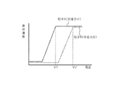
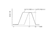
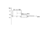
- the particles B having a larger adhesion force than the threshold voltage of the particles A Only the particles A are moved by applying a voltage V1 that is lower than the threshold voltage of.
- a weak electric field strength having a voltage smaller than the voltage V1 can be applied, so that the particle response time (image rewriting time) becomes long. That is, as shown in FIG. 2B, when the particles A are driven with different electric field strengths, the response is slowed down as the electric field strength decreases, so that the image rewriting time becomes long.
- each particle group starts to move simultaneously by application of a voltage. For this reason, it is difficult to completely separate and control the particle group, and there is a problem that color mixing occurs and image quality deteriorates.
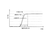
- the applicant of the present application appropriately designed the driving force and the adhesion force, so that the time that the particles do not immediately leave the substrate after applying a voltage between the electrodes (detachment start time) It was found that the particles were separated from the substrate with a certain distribution (withdrawal time distribution in FIG. 3A).
- FIG. 4A is a diagram showing a change in the amount of particles on the substrate when a certain voltage is applied to a certain particle group.
- the change in the amount of particles observes separation from the substrate and adhesion to the substrate (FIGS. 4B and 4C).
- the time from the start of detachment from the substrate to the end of detachment is the time from the start of detachment of the particle group to the end of detachment (detachment time distribution). It is significantly longer than the time (electrophoresis time) required for the particles to migrate between the substrates and reach the counter substrate.
- the desired particle group can be selectively moved by controlling the difference in the separation time without considering the difference in migration time (mobility) between the particle groups.
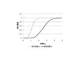
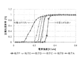
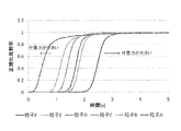
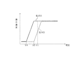
- FIG. 5A shows the normalized reflectance change when a voltage pulse having a constant time and different magnitude is applied to a plurality of particles A to F
- FIG. 5A shows the normalized reflectance change when a voltage pulse having a constant magnitude and a different length is applied.
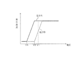
- the electric field strength (operation threshold) at which the particles start to move is The higher the particle size, the higher the particle.
- FIG. 5B when a voltage pulse having a constant magnitude is applied, the time for the particles to leave the substrate varies depending on the adhesion force of the particles, and the time for the particles to start moving (response time) is Particles with greater adhesion are longer.
- the particles can be selectively driven by controlling the voltage application time while keeping the voltage constant. It may be difficult to set so that they do not overlap.
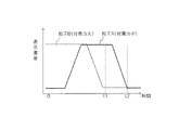
- the time for 80% of the particles to be separated is T80A, and among the particle group (particle B) having a long separation start time. If the time for 20% of particles to leave is T20B, a clear display with no color mixing is possible by designing T80A ⁇ T20B. Furthermore, as shown in FIG. 6B, by designing so that T95A ⁇ T5B, a preferable display with less color mixing can be obtained.
- the numerical values are not limited to the above.
- a voltage is applied for a time during which a predetermined A% (A> 50) of particles out of particles having a shorter time to start detachment from the substrate after voltage application is started. It may be set so that (100-A)% of the particles having a longer time to start detachment after the detachment will be shorter than the time for detachment.
- the saturation is reduced due to color mixing. Is prevented.
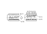
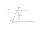
- FIG. 7A by applying a pulse application time shorter than the separation start time of the particle B, only the particle A moves to the display substrate 1 side and the color of the particle A is displayed as shown in FIG. 7B. Is done.
- FIG. 7C the color of the particle B is displayed as shown in FIG. 7D by applying a pulse application voltage that is equal to or longer than the time when all the particles A start to leave the back substrate 2 side.
- the separation time tends to increase as the surface charge density of the particles increases.
- the particle group having a longer separation time for example, the example of FIG. 8A.
- the particle B since the particle B) has a high migration speed, a part of the particle B may pass the particle A during the migration to cause color mixing as shown in FIG. 8B.
- the value of particle size d ⁇ surface charge density ⁇ of particle A is larger than the value of particle size d of particle B ⁇ surface charge density ⁇ .
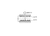
- the display side electrode 3 is grounded, and a voltage is applied to the back side electrode 4 will be described as an example.
- the first particle group 11 and the first particle group 11 are formed on the back substrate 2 side by applying a negative voltage that is equal to or higher than the operation threshold value of the particle group having the largest adhesion force among the plurality of types of particle groups.
- the two-particle group 12 is attached and driving is started as an initial state.
- the operation threshold voltage of the first particle group 11 is illustrated as VA
- the operation threshold voltage of the second particle group 12 is illustrated as VB.
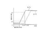
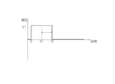
- FIG. 9A is a diagram showing an example of a drive pulse for displaying the color of the first particle group 11
- FIG. 9B is a diagram showing an example of change in display density with respect to the application time of the drive pulse in FIG. 9A.
- the operation threshold voltage VB of the particle group having the greatest adhesion force (second particle group 12 which is the particle group of the particle B) among the plurality of types of particle groups (FIG. 9C).
- a pulse voltage of a time t1 (FIG. 9A, FIG. 9B) of a length in which only a particle group (first particle group 11 which is a particle group of particle A) with a larger voltage V1 and a smaller adhesion force is separated is applied. .
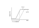
- FIG. 11A is a diagram illustrating an example of a drive pulse for displaying the color of the second particle group 12
- FIG. 11B is a diagram illustrating an example of change in display density with respect to the application time of the drive pulse in FIG. 11A.
- the operation threshold voltage VB (FIG. 11C) of the particle group having the greatest adhesion among the plurality of types of particle groups (the second particle group 12 that is the particle group of the particle B).
- a second pulse voltage is applied for a time (t2-t1) (FIGS. 11A and 11B) of a length for separating only the (first particle group 11) from the adhered substrate.
- FIG. 13A is a diagram showing an example of a drive pulse for gradation-displaying the color of the first particle group 12
- FIG. 13B is a diagram showing an example of change in display density with respect to the application time of the drive pulse in FIG. 13A
- FIG. 13C is a diagram showing the relationship between the voltages of the particles A and B and the display density.
- the operation threshold voltage VB (the second particle group 12 which is the particle group of the particle B) having the largest adhesion force among the plurality of types of particle groups ( FIG. 13C)
- a particle group (second particle group 12) having a higher voltage V1 and having a higher adhesion force does not leave, and only a part of the particle group (first particle group 11) having a lower adhesion force leaves.
- a pulse voltage of the time L 13 (t1 ⁇ L 13 ⁇ t2) (FIGS. 13A and 13B) is applied.
- the color of the first particle group 11 is displayed in gray scale by separating from the side, moving to the display substrate 1 side, and adhering. In this case, the color tone of the first particle group 11 is displayed in accordance with the length of time L 13.
- FIG. 15A is a diagram showing an example of a drive pulse for displaying the gradation of the color of the first particle group 12 and solving the unstable state
- FIG. 15B is a graph showing the display density with respect to the application time of the drive pulse of FIG. 15A. It is a figure which shows the example of a change
- FIG. 15C is a figure which shows the relationship between the voltage of particle
- the voltage V1 is larger than the operation threshold voltage VB (FIG. 15C) of the particle group having the largest adhesion force (second particle group 12 which is the particle group of the particle B) among the plurality of types of particle groups.
- the particle group (second particle group 12) having a large adhesion force does not leave, and a time L 13 (t1 ⁇ L) in which only a part of the particle group (first particle group 11) having a small adhesion force leaves. 13 ⁇ t2) (FIGS. 15A and 15B) is applied to perform gradation display of the color of the first particle group 11.
- V2 voltage smaller than the operating threshold voltage of any particle group
- the voltage V2 smaller than the operation threshold voltage of any particle group may be a negative voltage having a reverse polarity, as indicated by a dotted line in FIG. 15A. That is, an absolute value of a voltage smaller than the absolute value of the operation threshold voltage of any particle group may be applied as an auxiliary pulse.
- FIG. 17A is a diagram showing an example of a drive pulse for gradation-displaying the colors of the first particle group 11 and the second particle group 12, and FIG. 17B shows the relationship between the application time of the drive pulse of FIG. 17A and the display density.
- FIG. 17C is a diagram showing the relationship between the voltages of the particles A and B and the display density.
- the operation of the particle group having the greatest adhesion force among the plural types of particle groups (the second particle group 12 which is the particle group of the particle B).
- Time L 17-1 (t1 ⁇ L 17-1 ⁇ length of separation from the substrate to which the particle group (second particle group 12) having a high adhesion force and a voltage V1 larger than the threshold voltage VB (FIG. 17C) is adhered.
- t2 After applying the first pulse voltage of FIGS. 17A and 17B, subsequently, a particle group (first voltage) having a voltage ( ⁇ V1) having the same absolute value as that of the first pulse voltage, a different polarity ( ⁇ V1), and a large adhesion force.
- the length of time L 17-2 (t3 ⁇ t2 ⁇ L 17 ) in which the two particle groups 12) do not leave the adhered substrate, and only the particle group (first particle group 11) having a small adhesion force leaves the adhered substrate.
- ⁇ 2 ⁇ t4-t2 (second pulse voltage in FIGS. 17A and 17B) is applied.
- the first particle group 11 and the second particle group 12 are adhered to the back substrate 2 side by the application of the first pulse voltage, the first particle group 11 is detached from the back substrate 2 side until time t1.
- the second particle group 12 separates from the rear substrate 2 side and moves to the display substrate 1 side and adheres after the time t1 has elapsed.
- the gradation of the color of the second particle group 12 is controlled by adjusting the length of the time L 17-1 .
- the gradation of the color of the first particle group 11 is controlled by adjusting the length of the time L 17-2 .
- each particle group is attached to the back substrate 2 side as an initial state, but a state in which each particle group is attached to the display substrate 1 side may be the initial state.
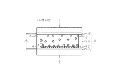
- the driving method in the case of three types of particle groups will be briefly described.
- a yellow particle group of particles A colored yellow, a magenta particle group of particles B colored magenta, and a cyan particle group of particles C colored cyan are encapsulated.
- the color is not limited to this.
- the adhesion force of each particle is such that particle A ⁇ particle B ⁇ particle C, and each particle is positively charged.
- the display side electrode 3 is grounded and a voltage is applied to the back side electrode 4 will be described.
- FIG. 18A is a diagram showing an example of driving pulses of three types of particles
- FIG. 18B is a diagram showing an example of changes in display density with respect to the application time of the driving pulse of FIG. 18A
- FIG. 18C is a diagram showing particles A, particles B, It is a figure which shows the relationship between the voltage of particle
- the movement of each particle is controlled by applying the first to third pulse voltages. That is, the voltage V1 is larger than the operation threshold voltage VC of the particle group (particle C) having the largest adhesion force among the plurality of types of particle groups, and the voltage for the application time according to the adhesion force of the particles to be detached from the substrate is imaged. Apply based on information.
- the movement of each particle can be selectively controlled by applying the first to third pulse voltages having different application times.
- a part of the particle C having the largest adhesion force is moved by the first pulse voltage (particle A and particle B all move).
- the gradation of the particle C is selected by adjusting the application time of the first pulse voltage between the times t1 and t2 shown in FIGS. 18A and 18B.
- a part of the particle B having the second largest adhesion force is moved by the second pulse voltage (the particle A all moves, and the particle C does not move).
- the gradation of the particle B is selected by adjusting the application time of the second pulse voltage between the times t3 and t4 shown in FIGS. 18A and 18B.
- the gradation of the particle A is selected by adjusting the application time of the third pulse voltage between the times t5 and t6 shown in FIGS. 18A and 18B.
- the first to third pulse voltages are (the length of the first pulse voltage)> (the length of the second pulse voltage)> (the length of the third pulse voltage), and the first pulse voltage has the largest adhesive force.
- the particle A is controlled, the particle B having the next largest adhesion force is controlled by the second pulse voltage, and the particle C having the smallest adhesion force is controlled by the third pulse voltage. That is, an image based on the image information is displayed by controlling the application time of the pulse voltage so that the particles are sequentially driven from the particles having the largest adhesive force.
- FIG. 19 shows an example in which the polarity of the second particle group 12 of the particle B is reversed (negatively charged) with respect to the example of FIG.
- the voltage V1 is larger than the operation threshold voltage VB (FIG.
- first particle group 11 is attached to the back substrate 2 side and the second particles 12 are attached to the display substrate 1 side by applying the first pulse voltage (FIG. 20A), as shown in FIG.
- Both the first particle group 11 and the second particle group 12 are detached from the substrate and moved to adhere to the opposite substrate (the first particle group 11 is separated from the rear substrate 2 side and moved to the display substrate 1 side.
- the second particle group 12 is detached from the display substrate 11 side and moves to the rear substrate 2 side and adheres).
- the first particle group 11 is detached from the display substrate 1 side, moves to the back substrate 2 side, and adheres to the display substrate 1 side.
- the group 11 and the second particle group 12 are both attached to the back substrate 2 side, and when the display medium is not displayed or the dispersion medium 6 is colored, the color of the dispersion medium 6 is displayed.
- a reset pulse for applying each particle group to a predetermined substrate is applied before the driving pulse. May be.
- the voltage and length of the reset pulse may be constant for all the pixels, or may be different for each pixel according to the previously displayed image.
- the second and subsequent pulses for selecting the moving particle amount of the particle group having the second largest adhesion force do not necessarily have the same absolute value as the first pulse. Since the voltage becomes constant by using a pulse having a magnitude equal to that of the first pulse, the device configuration is simple and inexpensive, but the second pulse can be used in response to a request for increasing the gradation resolution.
- the absolute values of the subsequent voltages may be varied.
- the particle group in the above embodiment may have a concealing property that absorbs a region other than the reflection wavelength region, but a highly transparent particle that absorbs only a specific wavelength region and transmits others. It is preferable for obtaining a vivid display.
- control unit 40 in the above embodiment may be realized by hardware, or may be realized by executing a software program.
- the program may be stored in various storage media and distributed.
- the image display medium drive device, image display device, drive program, and computer-readable medium according to the present invention are useful for, for example, display control of images displayed on electronic paper, electronic books, and the like.
Abstract
少なくとも一方が透光性を有する一対の基板間に封入され、予め定めた電圧の印加時に基板に付着した状態から離脱を開始する時間が各々異なる複数種類の粒子を有する画像表示媒体の前記一対の基板間に前記電圧を印加する電圧印加部と、前記一対の基板間に前記電圧を印加する時間を、画像情報に応じて可変するように前記電圧印加部を制御する制御部と、を備えた画像表示媒体の駆動装置が提供される。
Description
本発明は、画像表示媒体の駆動装置、画像表示装置、駆動プログラム、及びコンピュータ読み取り媒体に関する。
従来、メモリ性を有し繰り返し書換えが可能な画像表示媒体として、着色粒子を用いた画像表示媒体が知られている。このような画像表示媒体は、例えば一対の基板と、印加された電界により基板間を移動可能に基板間に封入されると共に、色及び帯電特性が異なる複数種類の粒子群と、を含んで構成される。
このような画像表示媒体では、画像に応じた電圧を一対の基板間に印加することにより粒子を移動させ、異なる色の粒子のコントラストとして画像を表示させる。また、画像を表示させた後に電圧の印加を停止した後も画像表示は維持される。
例えば、このような画像表示媒体としては、例えば、特許文献1、2に記載の技術が提案されている。
特許文献1には、黒色着色分散媒と、該分散媒中に分散され、互いに異なる色に着色され、かつ、互いに異なる電気泳動移動度を有する着色電気泳動粒子とを含む表示媒体を備え、該表示媒体に強度や向き、印加時間等の異なる電界をかけることにより異なる色彩の表示が行われる表示装置が開示されている。
特許文献2には、表示基板と背面基板との間の分散媒中に、表示基板及び背面基板に対する付着力、すなわち移動を開始する電界強度の異なる複数種類の粒子群を封入し、各粒子群の種類に応じて、各種類の粒子群が移動を開始する電界強度の電界を形成することで、選択的に所望の粒子を移動させて、所望の色以外の色の粒子が分散媒中を移動することを抑制して、所望の色以外の色が混じる混色を抑制することが開示されている。
本発明は、電圧の大きさを制御して粒子を駆動する場合よりも粒子の制御性を向上することを目的とする。
(1)本発明のある観点によれば、少なくとも一方が透光性を有する一対の基板間に封入され、予め定めた電圧の印加時に基板に付着した状態から離脱を開始する時間が各々異なる複数種類の粒子を有する画像表示媒体の前記一対の基板間に前記電圧を印加する電圧印加部と、前記一対の基板間に前記電圧を印加する時間を、画像情報に応じて可変するように前記電圧印加部を制御する制御部と、を備えた画像表示媒体の駆動装置である。
(2)本発明の他の観点によれば、少なくとも一方が透光性を有する一対の基板間に封入されると共に、種類毎に互い異なる色に着色され、かつ基板に付着した状態を維持するための付着力が種類毎にそれぞれ異なり、かつ基板に付着した状態から該基板離脱するために必要な電圧が種類毎にそれぞれ異なる複数種類の粒子を含み、画像情報に基づいて画像を表示する画像表示媒体の前記一対の基板間に電圧を印加する電圧印加部と、前記複数種類の粒子のうち付着力が最も大きい粒子が一方の基板に付着した状態から該基板を離脱する大きさの電圧を、該基板から離脱させるべき粒子の付着力に応じた印加時間で前記画像情報に基づいて前記一対の基板間に印加するように、前記電圧印加部を制御する制御部と、を備えた画像表示媒体の駆動装置である。
(3)前記制御部は、前記複数種類の粒子のうち前記付着力が最も大きい粒子が基板から離脱する大きさで、かつ前記印加時間として基板から離脱させるべき粒子の少なくとも一部が基板から離脱する時間の電圧を前記画像情報に基づいて前記一対の基板間に印加するように、前記電圧印加部を制御する(2)に記載の画像表示媒体の駆動装置である。
(4)前記制御部は、前記複数種類の粒子のうち前記付着力が最も大きい粒子が基板から離脱する大きさで、かつ前記印加時間として前記付着力が最も大きい粒子の少なくとも一部が基板から離脱する時間の電圧を印加した後に、前記付着力の大きい順に前記付着力に応じて順次前記印加時間及び極性を変えた電圧を前記画像情報に基づいて前記一対の基板間に印加するように、前記電圧印加部を制御する(2)に記載の画像表示媒体の駆動装置である。
(5)本発明の他の観点によれば、少なくとも一方が透光性を有する一対の基板間に封入されて帯電特性を有し、前記基板間に印加された電圧により付着した基板から離脱する粒子を含み、画像情報に基づいて画像を表示する画像表示媒体の前記一対の基板間に電圧を印加する電圧印加部と、前記粒子が基板に付着した状態から該粒子が該基板から離脱するために必要な付着力以上の大きさで、かつ前記粒子の少なくとも一部が前記基板から離脱する時間の電圧を前記画像情報に基づいて基板間に印加するように、前記電圧印加部を制御する制御部と、を備えた画像表示媒体の駆動装置である。
(6)前記複数種類の粒子は、前記基板から前記粒子が離脱を開始し始めてから全粒子が前記基板から離脱するまでの離脱時間分布をそれぞれ有し、該離脱時間分布に従って基板から離脱する(1)から(5)のいずれか一つに記載の画像表示媒体の駆動装置である。
(7)前記複数種類の粒子の各々の前記離脱時間分布は、前記電圧を印加開始してから前記基板から離脱開始する時間が短い方の粒子のうち予め定めたA%(A>50)の粒子が離脱する時間が、前記電圧を印加してから前記基板から離脱開始する時間が長い方の粒子のうち(100-A)%の粒子が離脱する時間よりも短い(6)に記載の画像表示媒体の駆動装置である。
(8)前記複数種類の粒子は、前記基板から離脱開始する時間が短い方の粒子の方が、前記基板から離脱開始する時間の長い方の粒子よりも、粒径×電荷密度が大きい(6)又は(7)に記載の画像表示媒体の駆動装置である。
(9)本発明の他の観点によれば、前記画像表示媒体と、(1)に記載の画像表示媒体の駆動装置と、を備えた画像表示装置である。
(10)本発明の他の観点によれば、前記画像表示媒体と、(2)から(4)のいずれか一つに記載の画像表示媒体の駆動装置と、を備えた画像表示装置である。
(11)本発明の他の観点によれば、前記画像表示媒体と、(5)に記載の画像表示媒体の駆動装置と、を備えた画像表示装置である。
(12)本発明の他の観点によれば、コンピュータを、(1)から(8)のいずれか一つに記載の画像表示媒体の駆動装置の前記制御部として機能させるための駆動プログラムである。
(13)本発明の他の観点によれば、コンピュータを、(1)から(8)のいずれか一つに記載の画像表示媒体の駆動装置の前記制御部として機能させるための駆動プログラムを記憶する非一時的なコンピュータ読み取り媒体である。
(13)本発明の他の観点によれば、コンピュータを、(1)から(8)のいずれか一つに記載の画像表示媒体の駆動装置の前記制御部として機能させるための駆動プログラムを記憶する非一時的なコンピュータ読み取り媒体である。
(1)に記載の構成によれば、電圧の大きさを制御して粒子を駆動する場合よりも粒子の制御性を向上することが可能な画像表示媒体の駆動装置を提供することができる。
(2)に記載の構成によれば、電圧の大きさを制御して粒子を駆動する場合よりも粒子の制御性を向上することが可能な画像表示媒体の駆動装置を提供することができる。
(3)に記載の構成によれば、基板から離脱させるべき粒子の階調表示が可能となる。
(4)に記載の構成によれば、複数種類の粒子を選択的に駆動することができる。
(5)に記載の構成によれば、電圧の大きさを制御して粒子を駆動する場合よりも画像の書換時間を短縮することが可能な画像表示装置の駆動装置を提供することができる。
(6)に記載の構成によれば、離脱時間分布を有さない場合に比べて粒子の制御性を向上することができる。
(7)に記載の構成によれば、本構成を採用しない場合に比べて混色のない鮮明な画像を得ることができる。
(8)に記載の構成によれば、後から基板を離脱した粒子が先に基板を離脱した粒子を追い越すことを防止することができる。
(9)に記載の構成によれば、電圧の大きさを制御して粒子を駆動する場合よりも粒子の制御性を向上することが可能な画像表示装置を提供することができる。
(10)に記載の構成によれば、電圧の大きさを制御して粒子を駆動する場合よりも粒子の制御性を向上することが可能な画像表示装置を提供することができる。
(11)に記載の構成によれば、電圧の大きさを制御して粒子を駆動する場合よりも粒子の制御性を向上することが可能な画像表示装置を提供することができる。
(12)に記載の構成によれば、電圧の大きさを制御して粒子を駆動する場合よりも画像の書換時間を短縮することが可能な駆動プログラムを提供することができる。
(13)に記載の構成によれば、電圧の大きさを制御して粒子を駆動する場合よりも画像の書換時間を短縮することが可能な駆動プログラムを記憶する非一時的なコンピュータ読み取り媒体を提供することができる。
(13)に記載の構成によれば、電圧の大きさを制御して粒子を駆動する場合よりも画像の書換時間を短縮することが可能な駆動プログラムを記憶する非一時的なコンピュータ読み取り媒体を提供することができる。
以下、本実施形態について図面を参照しつつ説明する。作用・機能が同じ働きを担う部材には、全図面を通して同じ符合を付与し、重複する説明を省略する場合がある。また、説明を簡易化するために、適宜1つのセルに注目した図を用いて本実施形態を説明する。なお、本発明の付着力とは、粒子が基板に付着した状態を維持するために必要な力のことを意味する。
図1Aは、本実施形態に係わる画像表示装置を概略的に示している。この画像表示装置100は、画像表示媒体10と、画像表示媒体10を駆動する駆動装置20と、を備えている。駆動装置20は、画像表示媒体10の表示側電極3、背面側電極4間に電圧を印加する電圧印加部30と、画像表示媒体10に表示させる画像の画像情報に応じて電圧印加部30を制御する制御部40と、を含んで構成されている。
画像表示媒体10は、画像表示面とされる、透光性を有する表示基板1と、非表示面とされる背面基板2と、が間隙を持って対向して配置される一対の基板を有する。
これらの基板1、2間を予め定められた間隔に保持すると共に、該基板間を複数のセルに区画する間隙部材5が設けられている。
上記セルとは、背面側電極4が設けられた背面基板2と、表示側電極3が設けられた表示基板1と、間隙部材5と、によって囲まれた領域を示している。セル中には、例えば絶縁性液体で構成された分散媒6と、分散媒6中に分散された第1粒子群11と、第2粒子群12とが封入されている。なお、第1粒子群11は後述する粒子Aの粒子群とされ、第2粒子群12は後述する粒子Bの粒子群とされている。
第1粒子群11と第2粒子群12は、互いに異なる色に着色されている。また、基板に付着した状態を維持するための付着力が互いに異なり、基板間の電界によって基板に付着した状態から基板を離脱するために必要な電圧が互いに異なる。そして、一対の電極3、4間に印加する電圧を制御することにより、第1粒子群11及び第2粒子群12がそれぞれ単独で泳動する特性を有している。より具体的には、電圧を印加して発生させた電界によって、粒子が基板を離脱する向きの力が付着力の大きさ以上になると粒子が基板を離脱して他方の基板に向かう。この、電界によって発生する力が付着力と釣り合って粒子が移動し始める電圧を閾値電圧という。本実施形態において、第1粒子群11と第2粒子群12を移動させ、画像を表示させた後に電圧の印加を停止した後も、ファンデルワールス力や鏡像力、静電引力等によって粒子は基板に付着したままとなり、画像表示は維持される。粒子の付着力を制御するには、これらの鏡像力や静電引力、ファンデルワールス力等を調整すればよく、その手段としては、例えば粒子の帯電量、粒径、電荷密度、誘電率、表面形状、表面エネルギー、分散剤の組成や密度等をそれぞれ適切に調整することが挙げられる。なお、第1粒子群11及び第2粒子群12の他に白色に着色された白色粒子群を含むようにしてもよい。この場合、白色粒子群は、第1粒子群11、第2粒子群12よりも帯電量が少なく、第1粒子群11、第2粒子群12がいずれか一方の電極側まで移動する電圧が電極間に印加されても、いずれの電極側まで移動しない粒子群とした浮遊粒子群としてもよい。或いは、第1粒子群11または第2粒子群12と浮遊粒子群の2種類の粒子群で構成するようにしてもよい。或いは、分散媒に着色剤を混合することで、泳動粒子の色とは異なる色(例えば、白色)を表示させる構成としてもよい。
駆動装置20(電圧印加部30及び制御部40)は、画像表示媒体10の表示側電極3、背面側電極4間に印加する電圧を表示させる色に応じて制御することにより、粒子群11、12を泳動させ、それぞれの帯電特性に応じて表示基板1、背面基板2のいずれか一方に引き付ける。
電圧印加部30は、表示側電極3及び背面側電極4にそれぞれ電気的に接続されている。また、電圧印加部30は、制御部40に信号授受されるように接続されている。
制御部40は、図1Bに示すように、例えばコンピュータ40として構成される。コンピュータ40は、一例として、CPU(Central Processing Unit)40A、ROM(Read Only Memory)40B、RAM(Random Access Memory)40C、不揮発性メモリ40D、及び入出力インターフェース(I/O)40Eがバス40Fを介して各々接続された構成であり、I/O40Eには電圧印加部30が接続されている。この場合、各色の表示に必要な電圧の印加を電圧印加部30に指示する処理をコンピュータ40に実行させるプログラムとして、例えば不揮発性メモリ40Dに書き込んでおき、これをCPU40Aが読み込んで実行させる。なお、プログラムは、CD-ROM等の記録媒体により提供するようにしてもよい。
電圧印加部30は、表示側電極3及び背面側電極4に電圧を印加するための電圧印加装置であり、制御部40の制御に応じた電圧を表示側電極3及び背面側電極4に印加する。電圧印加部30は、アクティブマトリクス方式を適用してもよいし、パッシブマトリクス方式を適用するようにしてもよい。或いは、セグメント方式を適用するようにしてもよい。
ところで、本実施形態における第1粒子群11や第2粒子群12のように、基板に付着した状態を維持するために必要な力(付着力)が異なる粒子群を駆動する方法としては、従来では、基板間に印加する電圧の大きさを制御することによって粒子群の移動を制御していた。また、互いに色の異なる粒子群を駆動する他の例では、粒子の泳動速度(移動度)の差を利用して粒子群の移動を制御していた。
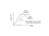
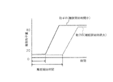
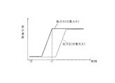
例えば、図2Aに示す動作閾値特性の粒子A及び粒子Bについて、付着力(動作閾値)の小さい粒子Aのみを移動させる場合には、粒子Aの閾値電圧よりも大きく、付着力の大きい粒子Bの閾値電圧よりも小さい、電圧V1を印加することによって粒子Aのみを移動するようにしていた。しかしながら、この方法では、粒子Aのみを移動させる場合、電圧V1より小さい電圧の弱い電界強度しか印加できないため、粒子の応答時間(画像の書き換え時間)が長くなってしまう。すなわち、図2Bに示すように、粒子Aを異なる電界強度で駆動したときには、電界強度が小さくなると応答が遅くなるので、画像の書き換え時間が長くなってしまう。
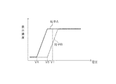
一方、移動度の差を利用して粒子群の移動を制御する場合には、図2Cに示すように、電圧の印加によって各粒子群が同時に動き始める。このため、粒子群を完全に分離して制御することが難しく、混色が発生して画質が劣化する問題があった。
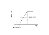
これに対して、本願出願人は、駆動力と付着力とを適切に設計することにより、電極間に電圧を印加してから粒子が直ちに基板から離脱せずに留まる時間(離脱開始時間)が発現し、粒子群がある分布(図3Aの離脱時間分布)を持って基板から離脱することを見出した。
すなわち、複数種類の粒子群の離脱開始時間を異ならせることで、図3Bに示すように、基板から離脱する離脱開始時間が異なる各粒子群を選択的に駆動することが可能となる。また、離脱時間分布を利用して、粒子群の一部の粒子を離脱させることで階調を制御することが可能となる。
図4Aは、ある粒子群に一定の電圧を以下したときの基板上の粒子量の変化を示す図である。粒子量の変化は、基板からの離脱や基板への付着を観察する(図4B、図4C)。
粒子群が基板から離脱開始してから離脱終了するまでの時間は、図4Aに示すように、粒子群の離脱開始から全粒子が離脱終了までの時間(離脱時間分布)の方が、離脱した粒子が基板間を泳動して対向基板に到達するのに要する時間(泳動時間)よりも大幅に長い。
従って、粒子群間の泳動時間(移動度)の差は考慮せず、離脱時間の差を制御することで、所望の粒子群を選択的に移動させることが可能となる。
また、図5Aは、複数の粒子A~Fに対して時間一定で大きさの異なる電圧パルスを印加した場合の正規化反射率変化を示し、図5Bは、複数の粒子A~Fに対して大きさが一定で長さの異なる電圧パルスを印加した場合の正規化反射率変化を示す。
図5Aに示すように、基板に付着した状態を維持するために必要な力(付着力)の異なる粒子に一定時間の電圧パルスを印加すると、粒子が動き始める電界強度(動作閾値)は、付着力の大きい粒子ほど高くなる。一方、図5Bに示すように、大きさが一定の電圧パルスを印加した場合、粒子が基板から離脱するための時間が粒子の付着力によって異なり、粒子が動き始める時間(応答時間)は、付着力の大きい粒子の方が長くなる。
そこで、本実施形態では、一定の大きさでかつ長さの異なる電圧パルスを印加することで、付着力の異なる粒子群のうち特定の粒子群のみを選択的に駆動するようになっている。
また、異なる電圧で印加時間の等しいパルスを印加した場合は、図5Aに示すように、電界-正規化反射率特性の傾きが粒子によって異なり、付着力が小さい方が傾きが緩くなる。一方、大きさが等しい電圧パルスを印加した場合には、図5Bに示すように、各粒子の時間-正規化反射率特性の傾きは概ね一定になり、特性曲線が並行にシフトした形となる。従って、本実施の形態のように、一定の大きさでかつ長さの異なる電圧パルスを印加した場合の方が、時間が一定で大きさの異なる電圧パルスを印加するよりも、各粒子群の独立制御性が向上する。
ところで、図5Bに示すように、粒子Aと粒子Bの離脱時間分布が重複しない場合には、電圧を一定として電圧印加時間を制御することで選択的に粒子を駆動できるが、離脱時間分布を重複しないように設定することが難しい場合がある。
この場合には、図6Aに示すように、離脱開始時間が短い粒子群(粒子A)のうち、80%の粒子が離脱する時間をT80A、離脱開始時間が長い粒子群(粒子B)のうち20%の粒子が離脱する時間をT20Bとすると、T80A<T20Bになるように設計することで、混色のない鮮明な表示が可能となる。さらに、図6Bに示すように、T95A<T5Bになるように設計することで、より混色のない好ましい表示が得られる。なお、数値は上記に限定されるものではない。すなわち、複数種類の粒子は、電圧を印加開始してから基板から離脱開始する時間が短い方の粒子のうち予め定めたA%(A>50)の粒子が離脱する時間が、電圧を印加してから離脱開始する時間が長い方の粒子のうち(100-A)%の粒子が離脱する時間よりも短くなるように設定してもよい。
また、各粒子群の離脱時間分布が完全に分離していない場合には、表示基板1側に一方の粒子群のみが付着するようにパルス印加電圧を制御することで、混色による彩度低下が防止される。例えば、図7Aの例では、粒子Bの離脱開始時間より短いパルス印加時間を印加することで、図7Bに示すように、粒子Aのみが表示基板1側に移動して粒子Aの色が表示される。また、図7Cの例では、粒子A全てが背面基板2側へ離脱開始する時間以上のパルス印加電圧を印加することで、図7Dに示すように、粒子Bの色が表示される。
また、本願出願人は、粒子の表面電荷密度が大きいほど離脱時間が長くなる傾向があることを見出した。そのような場合において、粒子が背面基板から表示基板方向へ移動する様子を観察したとき、各粒子群の平均粒径が同じであれば離脱時間の長い粒子群の方(例えば、図8Aの例では、粒子B)が泳動速度が速いため、図8Bに示すように、泳動中に粒子Bの一部が粒子Aを追い越して混色を生じる場合がある。
そこで、粒子Aと粒子Bの表面電荷密度の比を上回る比率でそれぞれの粒子群の平均粒径を異ならせることで、粒子Aの泳動速度の方が粒子Bよりも大きくなり、追い越しによる混色が防止される。
すなわち、泳動粒子の泳動速度vは、粒子の帯電量を、粒径をd、表面電荷密度をρ、分散媒の粘度をηとすると、v=(qE)/(6πηd)、q=4π(d/2)2ρで表されるので、v=(dρE)/6ηとなる。従って、粒径d×表面電荷密度ρを大きくすることにより、泳動速度を速くすることができる。例えば、図8Bの例では、図8Cに示すように、粒子Aの粒径d×表面電荷密度ρの値が、粒子Bの粒径d×表面電荷密度ρの値よりも大きくなるように、粒子Aの粒径dを粒子Bよりも大きく設定することにより、追い越しによる混色が防止される。
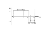
続いて、本実施形態に係わる画像表示装置の具体的な駆動方法について説明する。なお、以下では、第1粒子群11及び第2粒子群12は共に正に帯電し、一例として表示側電極3を接地し、背面側電極4に電圧を印加する場合について説明する。また、以下の説明では、複数種類の粒子群のうち最も付着力の大きい粒子群の動作閾値以上の負の電圧を基板間に印加することにより、背面基板2側に第1粒子群11及び第2粒子群12を付着させて初期状態として駆動を開始するものとする。また、以下の説明における図では、第1粒子群11の動作閾値電圧をVA、第2粒子群12の動作閾値電圧をVBとして図示する。
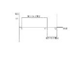
まず、第1粒子群11の色を表示する場合の駆動方法について説明する。図9Aは第1粒子群11の色を表示するための駆動パルスの一例を示す図であり、図9Bは図9Aの駆動パルスの印加時間に対する表示濃度の変化例を示す図であり、図9Cは粒子A及び粒子Bの電圧と表示濃度の関係を示す図である。
第1粒子群11の色を表示する場合には、複数種の粒子群のうち最も付着力の大きい粒子群(粒子Bの粒子群である第2粒子群12)の動作閾値電圧VB(図9C)より大きい電圧V1で、かつ付着力の小さい粒子群(粒子Aの粒子群である第1粒子群11)のみが離脱する長さの時間t1(図9A、図9B)のパルス電圧を印加する。
これにより、背面基板2側に第1粒子群11及び第2粒子群12が付着した初期状態(図10A)から、図10Bに示すように、第1粒子群11のみが背面基板2側から離脱して表示基板1側に移動して付着し第1粒子群11の色が表示される。
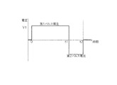
次に、第2粒子群12の色を表示する場合の駆動方法について説明する。図11Aは第2粒子群12の色を表示するための駆動パルスの一例を示す図であり、図11Bは図11Aの駆動パルスの印加時間に対する表示濃度の変化例を示す図であり、図11Cは粒子A及び粒子Bの電圧と表示濃度の関係を示す図である。
第2粒子群12の色を表示する場合には、複数種の粒子群のうち最も付着力が大きい粒子群(粒子Bの粒子群である第2粒子群12)の動作閾値電圧VB(図11C)より大きい電圧V1で、かつ付着力の大きい粒子群(第2粒子群12)が付着した基板から離脱する長さの時間t1(図11A、図11B)の第1パルス電圧を印加した後、続いて、第1パルス電圧と絶対値が等しく、極性が異なる電圧-V1で、かつ付着力の大きい粒子群(第2粒子群12)は付着した基板から離脱せず、付着力の小さい粒子群(第1粒子群11)のみが付着した基板から離脱する長さの時間(t2-t1)(図11A、図11B)の第2パルス電圧を印加する。
すなわち、第1パルス電圧の印加により、背面基板2側に第1粒子群11及び第2粒子群12が付着した状態(図12A)から、図12Bに示すように、第1粒子群11及び第2粒子群12が共に背面基板2側から離脱して表示基板1側に移動して付着する。
その後、第2パルス電圧の印加により、図12Cに示すように、第1粒子群11のみが表示基板1側から離脱して背面基板2側に移動して付着し第2粒子群12の色が表示される。
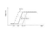
次に、第1粒子群11の色を階調表示するための駆動方法について説明する。図13Aは第1粒子群12の色を階調表示するための駆動パルスの一例を示す図であり、図13Bは図13Aの駆動パルスの印加時間に対する表示濃度の変化例を示す図であり、図13Cは粒子A及び粒子Bの電圧と表示濃度の関係を示す図である。
第1粒子群11の色を階調表示する場合には、複数種の粒子群のうち最も付着力の大きい粒子群(粒子Bの粒子群である第2粒子群12)の動作閾値電圧VB(図13C)より大きい電圧V1で、かつ付着力の大きい粒子群(第2粒子群12)は離脱せず、付着力の小さい粒子群(第1粒子群11)のうち一部のみが離脱する長さの時間L13(t1≦L13≦t2)(図13A、図13B)のパルス電圧を印加する。
これにより、背面基板2側に第1粒子群11及び第2粒子群12が付着した状態(図14A)から、図14Bに示すように、第1粒子群11のうち一部のみが背面基板2側から離脱して表示基板1側に移動して付着し第1粒子群11の色が階調表示される。このとき、時間L13の長さに応じた第1粒子群11の色の階調が表示される。
ここで、階調表示する場合には、図14Bに示すように、背面基板2側から離脱した第1粒子群11のうち表示基板1側に付着した粒子以外の粒子が浮遊している状態となって状態が不安定であるので、不安定な状態を解決するための駆動方法について説明する。図15Aは第1粒子群12の色を階調表示すると共に不安定な状態を解決するための駆動パルスの一例を示す図であり、図15Bは図15Aの駆動パルスの印加時間に対する表示濃度の変化例を示す図であり、図15Cは粒子A及び粒子Bの電圧と表示濃度の関係を示す図である。
まず、上記と同様に、複数種の粒子群のうち最も付着力の大きい粒子群(粒子Bの粒子群である第2粒子群12)の動作閾値電圧VB(図15C)より大きい電圧V1で、かつ付着力の大きい粒子群(第2粒子群12)は離脱せず、付着力の小さい粒子群(第1粒子群11)のうち一部のみが離脱する長さの時間L13(t1≦L13≦t2)(図15A、B)のパルス電圧を印加して、第1粒子群11の色の階調表示を行う。
その後続いて、いずれの粒子群の動作閾値電圧VA、VBより小さい電圧V2(図15A、図15C)で、時間L15(L15=t3-t2)の補助パルス電圧を印加する。この補助パルス電圧を印加すると、電圧V2はいずれの粒子群の動作閾値電圧よりも小さいため、背面基板2に付着している粒子はそのまま動かず、背面基板2側から離脱した第1粒子群11のうち基板間に浮遊した粒子のみが表示基板1側に移動して付着する。なお、いずれの粒子群の動作閾値電圧より小さい電圧V2は、図15Aの点線で示すように、逆極性のマイナスの電圧を印加するようにしてもよい。すなわち、いずれの粒子群の動作閾値電圧の絶対値より小さい電圧の絶対値を補助パルスとして印加するようにしてもよい。
これにより、背面基板2側に第1粒子群11及び第2粒子群12が付着した状態(図16A)から、図16Bに示すように、第1粒子群11のうち一部のみが背面基板2側から離脱して表示基板1側に移動して付着し第1粒子群11の色が階調表示される。そして、補助パルスによって浮遊している第1粒子群11の粒子が表示基板1側に移動して、図16Cに示すように、付着し安定した状態となる。また、マイナスの補助パルスを印加した場合には浮遊している第1粒子群11が背面基板2側に引き戻されて付着し安定した状態となる。
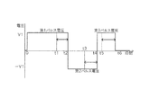
続いて、第1粒子群11及び第2粒子群12の色を階調表示するための駆動方法について説明する。図17Aは第1粒子群11及び第2粒子群12の色を階調表示するための駆動パルスの一例を示す図であり、図17Bは図17Aの駆動パルスの印加時間と表示濃度の関係を示す図であり、図17Cは粒子A及び粒子Bの電圧と表示濃度の関係を示す図である。
第1粒子群11及び第2粒子群12の色を表示する場合には、複数種の粒子群のうち最も付着力が大きい粒子群(粒子Bの粒子群である第2粒子群12)の動作閾値電圧VB(図17C)より大きい電圧V1で、かつ付着力の大きい粒子群(第2粒子群12)が付着した基板から離脱する長さの時間L17-1(t1≦L17-1≦t2)(図17A、B)の第1パルス電圧を印加した後、続いて、第1パルス電圧と絶対値が等しく、極性が異なる電圧(-V1)で、かつ付着力の大きい粒子群(第2粒子群12)は付着した基板から離脱せず、付着力の小さい粒子群(第1粒子群11)のみが付着した基板から離脱する長さの時間L17-2(t3-t2≦L17-2≦t4-t2)(図17A、B)の第2パルス電圧を印加する。
すなわち、第1パルス電圧の印加により、背面基板2側に第1粒子群11及び第2粒子群12が付着した状態から、時刻t1までは、第1粒子群11が背面基板2側から離脱して表示基板1側に移動して付着すると共に、時刻t1経過後は、第2粒子群12が背面基板2側から離脱して表示基板1側に移動して付着する。このとき、時間L17-1の長さを調整することで第2粒子群12の色の階調が制御される。
その後、第2パルス電圧の印加により、時刻t3経過後は、第1粒子群11のみが表示基板1側から離脱して背面基板2側に移動して付着する。このとき時間L17-2の長さを調整することで第1粒子群11の色の階調が制御される。
なお、上記の実施形態では、2種類の粒子群を封入した例について説明したが、粒子群は2種類に限るものではなく、3種類以上としてもよい。また、上記の実施形態では初期状態として背面基板2側に各粒子群を付着させた例を示したが、表示基板1側に各粒子群を付着させた状態を初期状態としてもよい。
ここで、3種類の粒子群の場合の駆動方法について簡単に説明する。以下では、3種類の粒子群として、黄色に着色された粒子Aの黄色粒子群、マゼンタ色に着色された粒子Bのマゼンタ粒子群、及びシアン色に着色された粒子Cのシアン粒子群が封入された画像表示装置の駆動方法について説明するが色はこれに限るものではない。また、各粒子の付着力は、粒子A<粒子B<粒子Cとされているものとし、それぞれ正に帯電しているものとして説明する。また、上記の実施形態と同様に、表示側電極3を接地し、背面側電極4に電圧を印加する場合について説明する。
図18Aは3種類の粒子の駆動パルスの一例を示す図であり、図18Bは図18Aの駆動パルスの印加時間に対する表示濃度の変化例を示す図であり、図18Cは粒子A、粒子B、及び粒子Cの電圧と表示濃度の関係を示す図である。
まず、複数種類の粒子群のうち最も付着力の大きい粒子Cの動作閾値以上の負の電圧を基板間に印加することにより、全ての粒子群を背面基板2側へ移動して初期状態を形成する。
3種類の粒子群の場合には、図18Aに示すように、第1~第3パルス電圧を印加することによって各粒子の移動を制御する。すなわち、複数種の粒子群のうち最も付着力が大きい粒子群(粒子C)の動作閾値電圧VCより大きい電圧V1で、かつ基板から離脱させるべき粒子の付着力に応じた印加時間の電圧を画像情報に基づいて印加する。3種類の粒子群の場合には、異なる印加時間の第1~第3パルス電圧を印加することにより、各粒子の移動を選択的に制御可能となる。
具体的には、第1パルス電圧で付着力の最も大きい粒子Cの一部を移動させる(粒子Aおよび粒子Bは全て移動する)。第1パルス電圧の印加する時間を、図18A、図18Bに示す時刻t1~t2の間で調整することで、粒子Cの階調が選択される。
次に、第2パルス電圧で付着力が次に大きい粒子Bの一部を移動させる(粒子Aは全て移動し、粒子Cは移動しない)。第2パルス電圧の印加する時間を、図18A、図18Bに示す時刻t3~t4の間で調整することで、粒子Bの階調が選択される。
続いて、第3パルス電圧で付着力が最も小さい粒子Aの一部を移動させる。第3パルス電圧の印加する時間を図18A、図18Bに示す時刻t5~t6の間で調整することで、粒子Aの階調が選択される。
第1~第3パルス電圧は、(第1パルス電圧の長さ)>(第2パルス電圧の長さ)>(第3パルス電圧の長さ)となり、第1パルス電圧によって付着力が最も大きい粒子Aを制御し、第2パルス電圧によって次に付着力が大きい粒子Bを制御し、第3パルス電圧によって付着力が最も小さい粒子Cを制御する。すなわち、付着力の大きい粒子から順に駆動するようにパルス電圧の印加時間を制御することで、画像情報に基づく画像が表示される。
なお、上記の実施形態では、複数種の粒子群はそれぞれ同極性に帯電している例を説明したが、同極性に限るものではなく、逆極性に帯電するようにしてもよく、同じ電圧印加時間で複数の粒子が移動しない特性の粒子であれば、複数種類の粒子を選択的に移動することができる。例えば、図11の例に対して粒子Bの第2粒子群12の極性を逆(負に帯電)にした場合の例を図19に示す。図19の例では、複数種の粒子群のうち最も付着力が大きい粒子群(粒子Bの粒子群である第2粒子群12)の動作閾値電圧VB(図19C)より大きい電圧V1で、かつ付着力の大きい粒子群(第2粒子群12)が付着した基板から離脱する長さの時間t1(図19A、図19B)の第1パルス電圧を印加した後、続いて、第1パルス電圧と絶対値が等しく、極性が異なる電圧-V1で、かつ付着力の大きい粒子群(第2粒子群12)は付着した基板から離脱せず、付着力の小さい粒子群(第1粒子群11)のみが付着した基板から離脱する長さの時間(t2-t1)(図19A、B)の第2パルス電圧を印加する。
すなわち、第1パルス電圧の印加により、背面基板2側に第1粒子群11が付着し、表示基板1側に第2粒子12が付着した状態(図20A)から、図20Bに示すように、第1粒子群11及び第2粒子群12が共に基板から離脱して反対側の基板に移動して付着する(第1粒子群11は背面基板2側から離脱して表示基板1側に移動して付着し、第2粒子群12は表示基板11側から離脱して背面基板2側に移動して付着する)。
その後、第2パルス電圧の印加により、図20Cに示すように、表示基板1側に第1粒子群11が表示基板1側から離脱して背面基板2側に移動して付着し、第1粒子群11及び第2粒子群12が共に背面基板2側に付着した状態となり、無表示或いは分散媒6が着色されている場合には分散媒6の色が表示される。
なお、本実施形態に係わる画像表示装置を駆動する際には、駆動パルスの前に、各粒子群を予め定めた基板に付着させる(全面を一定の色にする)リセットパルスを印加するようにしてもよい。リセットパルスの電圧及び長さは全画素で一定にしてもよいし、前に表示されていた画像に応じて画素毎に異ならせるようにしてもよい。
また、上記の実施形態において、付着力が2番目に大きい粒子群の移動粒子量を選択する第2パルス以降のパルスは、必ずしも第1パルスと絶対値が等しい大きさである必要はない。第1パルスと絶対値が等しい大きさのパルスを用いることで電圧が一定となるので、装置構成が簡単で安価な装置となるが、階調分解能を上げる等の要求に応じて、第2パルス以降の電圧の絶対値を異ならせてもよい。
また、上記の実施形態における粒子群は、反射波長域以外を吸収する隠蔽性を有するようにしてもよいが、特定の波長域のみを吸収し、その他は透過する透明性の高い粒子の方が、鮮やかな表示を得る上で好ましい。
また、上記の実施形態における制御部40が行う処理は、ハードウエアによって実現するようにしてもよいし、ソフトウエアのプログラムを実行することによって実現するようにしてもよい。また、当該プログラムは、各種記憶媒体に記憶して流通するようにしてもよい。
本発明に係る、画像表示媒体の駆動装置、画像表示装置、駆動プログラム及びコンピュータ読み取り媒体は、例えば、電子ペーパや電子書籍等に表示される画像の表示制御に用いるのに有用である。
本発明を詳細にまた特定の実施態様を参照して説明したが、本発明の精神と範囲を逸脱することなく様々な変更や修正を加えることができることは当業者にとって明らかである。
本出願は、2012年5月31日の日本特許出願(特願2012-124332)及び2013年3月13日の日本特許出願(特願2013-050392)に基づくものであり、その内容はここに参照として取り込まれる。
本出願は、2012年5月31日の日本特許出願(特願2012-124332)及び2013年3月13日の日本特許出願(特願2013-050392)に基づくものであり、その内容はここに参照として取り込まれる。
1 表示基板
2 背面基板
3 表示側電極
4 背面側電極
10 画像表示媒体
11 第1粒子群
12 第2粒子群
20 駆動装置
30 電圧印加部
40 制御部
100 画像表示装置
2 背面基板
3 表示側電極
4 背面側電極
10 画像表示媒体
11 第1粒子群
12 第2粒子群
20 駆動装置
30 電圧印加部
40 制御部
100 画像表示装置
Claims (13)
- 少なくとも一方が透光性を有する一対の基板間に封入され、予め定めた電圧の印加時に基板に付着した状態から離脱を開始する時間が各々異なる複数種類の粒子を有する画像表示媒体の前記一対の基板間に前記電圧を印加する電圧印加部と、
前記一対の基板間に前記電圧を印加する時間を、画像情報に応じて可変するように前記電圧印加部を制御する制御部と、
を備えた画像表示媒体の駆動装置。 - 少なくとも一方が透光性を有する一対の基板間に封入されると共に、種類毎に互い異なる色に着色され、かつ基板に付着した状態を維持するための付着力が種類毎にそれぞれ異なり、かつ基板に付着した状態から該基板離脱するために必要な電圧が種類毎にそれぞれ異なる複数種類の粒子を含み、画像情報に基づいて画像を表示する画像表示媒体の前記一対の基板間に電圧を印加する電圧印加部と、
前記複数種類の粒子のうち付着力が最も大きい粒子が一方の基板に付着した状態から該基板を離脱する大きさの電圧を、該基板から離脱させるべき粒子の付着力に応じた印加時間で前記画像情報に基づいて前記一対の基板間に印加するように、前記電圧印加部を制御する制御部と、
を備えた画像表示媒体の駆動装置。 - 前記制御部は、前記複数種類の粒子のうち前記付着力が最も大きい粒子が基板から離脱する大きさで、かつ前記印加時間として基板から離脱させるべき粒子の少なくとも一部が基板から離脱する時間の電圧を前記画像情報に基づいて前記一対の基板間に印加するように、前記電圧印加部を制御する請求項2に記載の画像表示媒体の駆動装置。
- 前記制御部は、前記複数種類の粒子のうち前記付着力が最も大きい粒子が基板から離脱する大きさで、かつ前記印加時間として前記付着力が最も大きい粒子の少なくとも一部が基板から離脱する時間の電圧を印加した後に、前記付着力の大きい順に前記付着力に応じて順次前記印加時間及び極性を変えた電圧を前記画像情報に基づいて前記一対の基板間に印加するように、前記電圧印加部を制御する請求項2に記載の画像表示媒体の駆動装置。
- 少なくとも一方が透光性を有する一対の基板間に封入されて帯電特性を有し、前記基板間に印加された電圧により付着した基板から離脱する粒子を含み、画像情報に基づいて画像を表示する画像表示媒体の前記一対の基板間に電圧を印加する電圧印加部と、
前記粒子が基板に付着した状態から該粒子が該基板から離脱するために必要な付着力以上の大きさで、かつ前記粒子の少なくとも一部が前記基板から離脱する時間の電圧を前記画像情報に基づいて基板間に印加するように、前記電圧印加部を制御する制御部と、
を備えた画像表示媒体の駆動装置。 - 前記複数種類の粒子は、前記基板から前記粒子が離脱を開始し始めてから全粒子が前記基板から離脱するまでの離脱時間分布をそれぞれ有し、該離脱時間分布に従って基板から離脱する請求項1から5のいずれか一項に記載の画像表示媒体の駆動装置。
- 前記複数種類の粒子の各々の前記離脱時間分布は、前記電圧を印加開始してから前記基板から離脱開始する時間が短い方の粒子のうち予め定めたA%(A>50)の粒子が離脱する時間が、前記電圧を印加してから前記基板から離脱開始する時間が長い方の粒子のうち(100-A)%の粒子が離脱する時間よりも短い請求項6に記載の画像表示媒体の駆動装置。
- 前記複数種類の粒子は、前記基板から離脱開始する時間が短い方の粒子の方が、前記基板から離脱開始する時間の長い方の粒子よりも、粒径×電荷密度が大きい請求項6又は7に記載の画像表示媒体の駆動装置。
- 前記画像表示媒体と、
請求項1に記載の画像表示媒体の駆動装置と、
を備えた画像表示装置。 - 前記画像表示媒体と、
請求項2から4のいずれか一項に記載の画像表示媒体の駆動装置と、
を備えた画像表示装置。 - 前記画像表示媒体と、
請求項5に記載の画像表示媒体の駆動装置と、
を備えた画像表示装置。 - コンピュータを、請求項1から8のいずれか一項に記載の画像表示媒体の駆動装置の前記制御部として機能させるための駆動プログラム。
- コンピュータを、請求項1から8のいずれか一項に記載の画像表示媒体の駆動装置の前記制御部として機能させるための駆動プログラムを記憶する非一時的なコンピュータ読み取り媒体。
Priority Applications (2)
| Application Number | Priority Date | Filing Date | Title |
|---|---|---|---|
| US14/386,129 US9779671B2 (en) | 2012-05-31 | 2013-05-31 | Image display medium driving device, image display apparatus, driving program, and computer-readable medium |
| US15/689,199 US10157581B2 (en) | 2012-05-31 | 2017-08-29 | Image display medium driving device, image display apparatus, driving program, and computer-readable medium |
Applications Claiming Priority (4)
| Application Number | Priority Date | Filing Date | Title |
|---|---|---|---|
| JP2012124332 | 2012-05-31 | ||
| JP2012-124332 | 2012-05-31 | ||
| JP2013050392A JP5935064B2 (ja) | 2012-05-31 | 2013-03-13 | 画像表示媒体の駆動装置、画像表示装置、及び駆動プログラム |
| JP2013-050392 | 2013-03-13 |
Related Child Applications (2)
| Application Number | Title | Priority Date | Filing Date |
|---|---|---|---|
| US14/386,129 A-371-Of-International US9779671B2 (en) | 2012-05-31 | 2013-05-31 | Image display medium driving device, image display apparatus, driving program, and computer-readable medium |
| US15/689,199 Division US10157581B2 (en) | 2012-05-31 | 2017-08-29 | Image display medium driving device, image display apparatus, driving program, and computer-readable medium |
Publications (1)
| Publication Number | Publication Date |
|---|---|
| WO2013180276A1 true WO2013180276A1 (ja) | 2013-12-05 |
Family
ID=49673459
Family Applications (1)
| Application Number | Title | Priority Date | Filing Date |
|---|---|---|---|
| PCT/JP2013/065212 WO2013180276A1 (ja) | 2012-05-31 | 2013-05-31 | 画像表示媒体の駆動装置、画像表示装置、駆動プログラム、及びコンピュータ読み取り媒体 |
Country Status (3)
| Country | Link |
|---|---|
| US (2) | US9779671B2 (ja) |
| JP (1) | JP5935064B2 (ja) |
| WO (1) | WO2013180276A1 (ja) |
Families Citing this family (7)
| Publication number | Priority date | Publication date | Assignee | Title |
|---|---|---|---|---|
| JP6362354B2 (ja) * | 2014-03-03 | 2018-07-25 | イー インク コーポレイション | 画像表示装置、画像表示制御装置、及び画像表示プログラム |
| RU2760510C1 (ru) | 2018-11-30 | 2021-11-25 | Е Инк Калифорния, Ллс | Электрооптические дисплеи и способы их возбуждения |
| KR102156044B1 (ko) * | 2019-08-13 | 2020-09-15 | 엔스펙트라 주식회사 | 디스플레이 패널 구조 및 이의 구동 방법 |
| CN114503026A (zh) * | 2019-08-13 | 2022-05-13 | 奈斯派克特株式会社 | 显示面板结构及其驱动方法 |
| WO2021221358A1 (ko) * | 2020-04-29 | 2021-11-04 | 엘지이노텍 주식회사 | 광 경로 제어 부재 및 이를 포함하는 디스플레이 장치 |
| JP2023527541A (ja) | 2020-06-05 | 2023-06-29 | イー インク カリフォルニア, エルエルシー | 電気泳動ディスプレイデバイス |
| WO2023034683A1 (en) | 2021-09-06 | 2023-03-09 | E Ink California, Llc | Method for driving electrophoretic display device |
Citations (3)
| Publication number | Priority date | Publication date | Assignee | Title |
|---|---|---|---|---|
| JP2001290178A (ja) * | 2000-02-04 | 2001-10-19 | Fuji Xerox Co Ltd | 画像表示装置、画像表示媒体、及び画像表示制御装置 |
| JP2008176017A (ja) * | 2007-01-18 | 2008-07-31 | Brother Ind Ltd | 電気泳動表示媒体及び電気泳動表示装置 |
| JP2009244635A (ja) * | 2008-03-31 | 2009-10-22 | Brother Ind Ltd | 粒子移動式表示装置及び該粒子移動式表示装置を備えた画像表示装置 |
Family Cites Families (39)
| Publication number | Priority date | Publication date | Assignee | Title |
|---|---|---|---|---|
| JP2000194021A (ja) | 1998-12-28 | 2000-07-14 | Sony Corp | 表示装置 |
| US6531997B1 (en) * | 1999-04-30 | 2003-03-11 | E Ink Corporation | Methods for addressing electrophoretic displays |
| JP3726646B2 (ja) * | 1999-07-21 | 2005-12-14 | 富士ゼロックス株式会社 | 画像表示方法、画像表示装置、及び画像表示媒体 |
| JP4126851B2 (ja) * | 1999-07-21 | 2008-07-30 | 富士ゼロックス株式会社 | 画像表示媒体、画像形成方法、及び画像形成装置 |
| US6636186B1 (en) | 2000-02-04 | 2003-10-21 | Fuji Xerox Co., Ltd | Image display medium, device and method |
| JP3750565B2 (ja) * | 2000-06-22 | 2006-03-01 | セイコーエプソン株式会社 | 電気泳動表示装置の駆動方法、駆動回路、および電子機器 |
| US7230750B2 (en) * | 2001-05-15 | 2007-06-12 | E Ink Corporation | Electrophoretic media and processes for the production thereof |
| JP4196555B2 (ja) * | 2001-09-28 | 2008-12-17 | 富士ゼロックス株式会社 | 画像表示装置 |
| US7952557B2 (en) * | 2001-11-20 | 2011-05-31 | E Ink Corporation | Methods and apparatus for driving electro-optic displays |
| US9412314B2 (en) * | 2001-11-20 | 2016-08-09 | E Ink Corporation | Methods for driving electro-optic displays |
| EP1462847A4 (en) | 2001-12-10 | 2005-11-16 | Bridgestone Corp | VIEW |
| AU2003207186A1 (en) | 2002-02-15 | 2003-09-04 | Bridgestone Corporation | Image display unit |
| US7321459B2 (en) | 2002-03-06 | 2008-01-22 | Bridgestone Corporation | Image display device and method |
| JP3960084B2 (ja) * | 2002-03-06 | 2007-08-15 | セイコーエプソン株式会社 | ヘッド駆動装置及び方法、液滴吐出装置、ヘッド駆動プログラム、並びにデバイス製造方法及びデバイス |
| AU2003235217A1 (en) | 2002-04-17 | 2003-10-27 | Bridgestone Corporation | Image display unit |
| CN1324392C (zh) | 2002-04-26 | 2007-07-04 | 株式会社普利司通 | 用于图像显示的颗粒和设备 |
| AU2003244117A1 (en) | 2002-06-21 | 2004-01-06 | Bridgestone Corporation | Image display and method for manufacturing image display |
| US20060087489A1 (en) | 2002-07-17 | 2006-04-27 | Ryou Sakurai | Image display |
| GB0218776D0 (en) * | 2002-08-13 | 2002-09-18 | Qinetiq Ltd | Phoretic display device |
| TW200410034A (en) * | 2002-11-28 | 2004-06-16 | Matsushita Electric Ind Co Ltd | Display device and manufacturing method thereof |
| US7495819B2 (en) | 2002-12-17 | 2009-02-24 | Bridgestone Corporation | Method of manufacturing image display panel, method of manufacturing image display device, and image display device |
| US7050040B2 (en) * | 2002-12-18 | 2006-05-23 | Xerox Corporation | Switching of two-particle electrophoretic display media with a combination of AC and DC electric field for contrast enhancement |
| AU2003289452A1 (en) | 2002-12-24 | 2004-07-22 | Bridgestone Corporation | Image display |
| WO2004077140A1 (ja) | 2003-02-25 | 2004-09-10 | Bridgestone Corporation | 画像表示用パネル及び画像表示装置 |
| JPWO2004079442A1 (ja) | 2003-03-06 | 2006-06-08 | 株式会社ブリヂストン | 画像表示装置の製造方法及び画像表示装置 |
| WO2004090626A1 (ja) | 2003-04-02 | 2004-10-21 | Bridgestone Corporation | 画像表示媒体に用いる粒子、それを用いた画像表示用パネル及び画像表示装置 |
| WO2005029458A1 (en) * | 2003-09-19 | 2005-03-31 | E Ink Corporation | Methods for reducing edge effects in electro-optic displays |
| KR100502358B1 (ko) * | 2003-10-14 | 2005-07-20 | 삼성에스디아이 주식회사 | 어드레스-디스플레이 혼합에 의한 방전 디스플레이 패널의구동 방법 |
| US8164557B2 (en) * | 2004-10-29 | 2012-04-24 | Semiconductor Energy Laboratory Co., Ltd. | Liquid crystal display device and method for driving the same |
| CA2510855A1 (en) * | 2005-07-06 | 2007-01-06 | Ignis Innovation Inc. | Fast driving method for amoled displays |
| JP2007108355A (ja) * | 2005-10-12 | 2007-04-26 | Seiko Epson Corp | 表示制御装置、表示装置及び表示装置の制御方法 |
| JP5119674B2 (ja) | 2006-02-14 | 2013-01-16 | 富士ゼロックス株式会社 | 画像表示媒体、画像表示装置、書込装置、及び画像表示プログラム |
| JP5023906B2 (ja) * | 2007-09-12 | 2012-09-12 | ソニー株式会社 | 表示装置及び表示装置の駆動方法 |
| JPWO2009075356A1 (ja) | 2007-12-13 | 2011-04-28 | 株式会社ブリヂストン | 情報表示用パネルの駆動方法および情報表示用パネル |
| WO2011077668A1 (ja) | 2009-12-25 | 2011-06-30 | 株式会社ブリヂストン | 情報表示用パネル及びその製造方法 |
| KR102581069B1 (ko) * | 2010-02-05 | 2023-09-20 | 가부시키가이샤 한도오따이 에네루기 켄큐쇼 | 반도체 장치, 및 반도체 장치의 제조 방법 |
| JP5625974B2 (ja) * | 2011-02-09 | 2014-11-19 | セイコーエプソン株式会社 | 電気泳動表示シート、電気泳動表示シートの製造方法および電子機器。 |
| US8941583B2 (en) * | 2011-02-15 | 2015-01-27 | Copytele, Inc. | Dual particle electrophoretic display and method of manufacturing same |
| KR101392583B1 (ko) * | 2012-11-02 | 2014-05-12 | 청운대학교산학협력단 | 반사형 컬러 표시 장치 |
-
2013
- 2013-03-13 JP JP2013050392A patent/JP5935064B2/ja active Active
- 2013-05-31 WO PCT/JP2013/065212 patent/WO2013180276A1/ja active Application Filing
- 2013-05-31 US US14/386,129 patent/US9779671B2/en active Active
-
2017
- 2017-08-29 US US15/689,199 patent/US10157581B2/en active Active
Patent Citations (3)
| Publication number | Priority date | Publication date | Assignee | Title |
|---|---|---|---|---|
| JP2001290178A (ja) * | 2000-02-04 | 2001-10-19 | Fuji Xerox Co Ltd | 画像表示装置、画像表示媒体、及び画像表示制御装置 |
| JP2008176017A (ja) * | 2007-01-18 | 2008-07-31 | Brother Ind Ltd | 電気泳動表示媒体及び電気泳動表示装置 |
| JP2009244635A (ja) * | 2008-03-31 | 2009-10-22 | Brother Ind Ltd | 粒子移動式表示装置及び該粒子移動式表示装置を備えた画像表示装置 |
Also Published As
| Publication number | Publication date |
|---|---|
| JP2014006495A (ja) | 2014-01-16 |
| US9779671B2 (en) | 2017-10-03 |
| US20170358263A1 (en) | 2017-12-14 |
| JP5935064B2 (ja) | 2016-06-15 |
| US20150138247A1 (en) | 2015-05-21 |
| US10157581B2 (en) | 2018-12-18 |
Similar Documents
| Publication | Publication Date | Title |
|---|---|---|
| WO2013180276A1 (ja) | 画像表示媒体の駆動装置、画像表示装置、駆動プログラム、及びコンピュータ読み取り媒体 | |
| JP5304850B2 (ja) | 表示媒体の駆動装置、駆動プログラム、及び表示装置 | |
| JP6235196B2 (ja) | 表示媒体の駆動装置、駆動プログラム、及び表示装置 | |
| US9779670B2 (en) | Driving device of display medium, non-transitory computer readable medium storing driving program of display medium, and display | |
| JP6284294B2 (ja) | 画像表示媒体の駆動装置、画像表示装置、及び駆動プログラム | |
| JP5996277B2 (ja) | 画像表示媒体、及び画像表示装置 | |
| US9424800B2 (en) | Driving device of image display medium, image display apparatus, and non-transitory computer readable medium | |
| JP6182330B2 (ja) | 画像表示媒体の駆動装置、画像表示装置、及び駆動プログラム | |
| JP2013250384A (ja) | 表示媒体の駆動装置、駆動プログラム、及び表示装置 | |
| JP6371078B2 (ja) | 画像表示装置、画像表示制御装置、及び画像表示プログラム | |
| JP6362354B2 (ja) | 画像表示装置、画像表示制御装置、及び画像表示プログラム | |
| JP6522881B2 (ja) | 表示媒体の駆動装置、表示媒体の駆動プログラム、及び表示装置 | |
| JP5287952B2 (ja) | 表示媒体の駆動装置、駆動プログラム、及び表示装置 | |
| JP6343157B2 (ja) | 表示媒体の駆動装置、表示媒体の駆動プログラム、及び表示装置 | |
| JP2016194730A (ja) | 画像表示媒体、及び画像表示装置 | |
| JP6307569B2 (ja) | 表示媒体の駆動装置、駆動プログラム、及び表示装置 | |
| JP5382073B2 (ja) | 表示媒体の駆動装置、駆動プログラム、及び表示装置 | |
| JP2017016140A (ja) | 画像表示媒体の駆動装置、画像表示装置、及び駆動プログラム |
Legal Events
| Date | Code | Title | Description |
|---|---|---|---|
| 121 | Ep: the epo has been informed by wipo that ep was designated in this application |
Ref document number: 13796911 Country of ref document: EP Kind code of ref document: A1 |
|
| WWE | Wipo information: entry into national phase |
Ref document number: 14386129 Country of ref document: US |
|
| NENP | Non-entry into the national phase |
Ref country code: DE |
|
| 122 | Ep: pct application non-entry in european phase |
Ref document number: 13796911 Country of ref document: EP Kind code of ref document: A1 |