WO2013179879A1 - 半導体モジュール及び半導体モジュールの製造方法 - Google Patents
半導体モジュール及び半導体モジュールの製造方法 Download PDFInfo
- Publication number
- WO2013179879A1 WO2013179879A1 PCT/JP2013/063290 JP2013063290W WO2013179879A1 WO 2013179879 A1 WO2013179879 A1 WO 2013179879A1 JP 2013063290 W JP2013063290 W JP 2013063290W WO 2013179879 A1 WO2013179879 A1 WO 2013179879A1
- Authority
- WO
- WIPO (PCT)
- Prior art keywords
- region
- frame
- semiconductor module
- frame body
- wiring board
- Prior art date
Links
Images


Classifications
-
- H—ELECTRICITY
- H01—ELECTRIC ELEMENTS
- H01L—SEMICONDUCTOR DEVICES NOT COVERED BY CLASS H10
- H01L23/00—Details of semiconductor or other solid state devices
- H01L23/48—Arrangements for conducting electric current to or from the solid state body in operation, e.g. leads, terminal arrangements ; Selection of materials therefor
- H01L23/50—Arrangements for conducting electric current to or from the solid state body in operation, e.g. leads, terminal arrangements ; Selection of materials therefor for integrated circuit devices, e.g. power bus, number of leads
-
- H—ELECTRICITY
- H01—ELECTRIC ELEMENTS
- H01L—SEMICONDUCTOR DEVICES NOT COVERED BY CLASS H10
- H01L23/00—Details of semiconductor or other solid state devices
- H01L23/02—Containers; Seals
- H01L23/04—Containers; Seals characterised by the shape of the container or parts, e.g. caps, walls
- H01L23/053—Containers; Seals characterised by the shape of the container or parts, e.g. caps, walls the container being a hollow construction and having an insulating or insulated base as a mounting for the semiconductor body
-
- H—ELECTRICITY
- H01—ELECTRIC ELEMENTS
- H01L—SEMICONDUCTOR DEVICES NOT COVERED BY CLASS H10
- H01L25/00—Assemblies consisting of a plurality of individual semiconductor or other solid state devices ; Multistep manufacturing processes thereof
- H01L25/50—Multistep manufacturing processes of assemblies consisting of devices, each device being of a type provided for in group H01L27/00 or H01L29/00
-
- H—ELECTRICITY
- H01—ELECTRIC ELEMENTS
- H01L—SEMICONDUCTOR DEVICES NOT COVERED BY CLASS H10
- H01L2224/00—Indexing scheme for arrangements for connecting or disconnecting semiconductor or solid-state bodies and methods related thereto as covered by H01L24/00
- H01L2224/01—Means for bonding being attached to, or being formed on, the surface to be connected, e.g. chip-to-package, die-attach, "first-level" interconnects; Manufacturing methods related thereto
- H01L2224/42—Wire connectors; Manufacturing methods related thereto
- H01L2224/47—Structure, shape, material or disposition of the wire connectors after the connecting process
- H01L2224/48—Structure, shape, material or disposition of the wire connectors after the connecting process of an individual wire connector
- H01L2224/481—Disposition
- H01L2224/48151—Connecting between a semiconductor or solid-state body and an item not being a semiconductor or solid-state body, e.g. chip-to-substrate, chip-to-passive
- H01L2224/48221—Connecting between a semiconductor or solid-state body and an item not being a semiconductor or solid-state body, e.g. chip-to-substrate, chip-to-passive the body and the item being stacked
- H01L2224/48225—Connecting between a semiconductor or solid-state body and an item not being a semiconductor or solid-state body, e.g. chip-to-substrate, chip-to-passive the body and the item being stacked the item being non-metallic, e.g. insulating substrate with or without metallisation
- H01L2224/48227—Connecting between a semiconductor or solid-state body and an item not being a semiconductor or solid-state body, e.g. chip-to-substrate, chip-to-passive the body and the item being stacked the item being non-metallic, e.g. insulating substrate with or without metallisation connecting the wire to a bond pad of the item
-
- H—ELECTRICITY
- H01—ELECTRIC ELEMENTS
- H01L—SEMICONDUCTOR DEVICES NOT COVERED BY CLASS H10
- H01L2224/00—Indexing scheme for arrangements for connecting or disconnecting semiconductor or solid-state bodies and methods related thereto as covered by H01L24/00
- H01L2224/01—Means for bonding being attached to, or being formed on, the surface to be connected, e.g. chip-to-package, die-attach, "first-level" interconnects; Manufacturing methods related thereto
- H01L2224/42—Wire connectors; Manufacturing methods related thereto
- H01L2224/47—Structure, shape, material or disposition of the wire connectors after the connecting process
- H01L2224/49—Structure, shape, material or disposition of the wire connectors after the connecting process of a plurality of wire connectors
- H01L2224/491—Disposition
- H01L2224/4911—Disposition the connectors being bonded to at least one common bonding area, e.g. daisy chain
- H01L2224/49111—Disposition the connectors being bonded to at least one common bonding area, e.g. daisy chain the connectors connecting two common bonding areas, e.g. Litz or braid wires
-
- H—ELECTRICITY
- H01—ELECTRIC ELEMENTS
- H01L—SEMICONDUCTOR DEVICES NOT COVERED BY CLASS H10
- H01L2224/00—Indexing scheme for arrangements for connecting or disconnecting semiconductor or solid-state bodies and methods related thereto as covered by H01L24/00
- H01L2224/01—Means for bonding being attached to, or being formed on, the surface to be connected, e.g. chip-to-package, die-attach, "first-level" interconnects; Manufacturing methods related thereto
- H01L2224/42—Wire connectors; Manufacturing methods related thereto
- H01L2224/47—Structure, shape, material or disposition of the wire connectors after the connecting process
- H01L2224/49—Structure, shape, material or disposition of the wire connectors after the connecting process of a plurality of wire connectors
- H01L2224/491—Disposition
- H01L2224/4912—Layout
- H01L2224/49175—Parallel arrangements
-
- H—ELECTRICITY
- H01—ELECTRIC ELEMENTS
- H01L—SEMICONDUCTOR DEVICES NOT COVERED BY CLASS H10
- H01L2224/00—Indexing scheme for arrangements for connecting or disconnecting semiconductor or solid-state bodies and methods related thereto as covered by H01L24/00
- H01L2224/73—Means for bonding being of different types provided for in two or more of groups H01L2224/10, H01L2224/18, H01L2224/26, H01L2224/34, H01L2224/42, H01L2224/50, H01L2224/63, H01L2224/71
- H01L2224/732—Location after the connecting process
- H01L2224/73251—Location after the connecting process on different surfaces
- H01L2224/73265—Layer and wire connectors
-
- H—ELECTRICITY
- H01—ELECTRIC ELEMENTS
- H01L—SEMICONDUCTOR DEVICES NOT COVERED BY CLASS H10
- H01L2224/00—Indexing scheme for arrangements for connecting or disconnecting semiconductor or solid-state bodies and methods related thereto as covered by H01L24/00
- H01L2224/80—Methods for connecting semiconductor or other solid state bodies using means for bonding being attached to, or being formed on, the surface to be connected
- H01L2224/85—Methods for connecting semiconductor or other solid state bodies using means for bonding being attached to, or being formed on, the surface to be connected using a wire connector
- H01L2224/8538—Bonding interfaces outside the semiconductor or solid-state body
- H01L2224/85399—Material
- H01L2224/854—Material with a principal constituent of the material being a metal or a metalloid, e.g. boron (B), silicon (Si), germanium (Ge), arsenic (As), antimony (Sb), tellurium (Te) and polonium (Po), and alloys thereof
- H01L2224/85401—Material with a principal constituent of the material being a metal or a metalloid, e.g. boron (B), silicon (Si), germanium (Ge), arsenic (As), antimony (Sb), tellurium (Te) and polonium (Po), and alloys thereof the principal constituent melting at a temperature of less than 400°C
- H01L2224/85411—Tin (Sn) as principal constituent
-
- H—ELECTRICITY
- H01—ELECTRIC ELEMENTS
- H01L—SEMICONDUCTOR DEVICES NOT COVERED BY CLASS H10
- H01L2224/00—Indexing scheme for arrangements for connecting or disconnecting semiconductor or solid-state bodies and methods related thereto as covered by H01L24/00
- H01L2224/80—Methods for connecting semiconductor or other solid state bodies using means for bonding being attached to, or being formed on, the surface to be connected
- H01L2224/85—Methods for connecting semiconductor or other solid state bodies using means for bonding being attached to, or being formed on, the surface to be connected using a wire connector
- H01L2224/8538—Bonding interfaces outside the semiconductor or solid-state body
- H01L2224/85399—Material
- H01L2224/854—Material with a principal constituent of the material being a metal or a metalloid, e.g. boron (B), silicon (Si), germanium (Ge), arsenic (As), antimony (Sb), tellurium (Te) and polonium (Po), and alloys thereof
- H01L2224/85438—Material with a principal constituent of the material being a metal or a metalloid, e.g. boron (B), silicon (Si), germanium (Ge), arsenic (As), antimony (Sb), tellurium (Te) and polonium (Po), and alloys thereof the principal constituent melting at a temperature of greater than or equal to 950°C and less than 1550°C
- H01L2224/85439—Silver (Ag) as principal constituent
-
- H—ELECTRICITY
- H01—ELECTRIC ELEMENTS
- H01L—SEMICONDUCTOR DEVICES NOT COVERED BY CLASS H10
- H01L2224/00—Indexing scheme for arrangements for connecting or disconnecting semiconductor or solid-state bodies and methods related thereto as covered by H01L24/00
- H01L2224/80—Methods for connecting semiconductor or other solid state bodies using means for bonding being attached to, or being formed on, the surface to be connected
- H01L2224/85—Methods for connecting semiconductor or other solid state bodies using means for bonding being attached to, or being formed on, the surface to be connected using a wire connector
- H01L2224/8538—Bonding interfaces outside the semiconductor or solid-state body
- H01L2224/85399—Material
- H01L2224/854—Material with a principal constituent of the material being a metal or a metalloid, e.g. boron (B), silicon (Si), germanium (Ge), arsenic (As), antimony (Sb), tellurium (Te) and polonium (Po), and alloys thereof
- H01L2224/85438—Material with a principal constituent of the material being a metal or a metalloid, e.g. boron (B), silicon (Si), germanium (Ge), arsenic (As), antimony (Sb), tellurium (Te) and polonium (Po), and alloys thereof the principal constituent melting at a temperature of greater than or equal to 950°C and less than 1550°C
- H01L2224/85444—Gold (Au) as principal constituent
-
- H—ELECTRICITY
- H01—ELECTRIC ELEMENTS
- H01L—SEMICONDUCTOR DEVICES NOT COVERED BY CLASS H10
- H01L23/00—Details of semiconductor or other solid state devices
- H01L23/34—Arrangements for cooling, heating, ventilating or temperature compensation ; Temperature sensing arrangements
- H01L23/36—Selection of materials, or shaping, to facilitate cooling or heating, e.g. heatsinks
- H01L23/373—Cooling facilitated by selection of materials for the device or materials for thermal expansion adaptation, e.g. carbon
-
- H—ELECTRICITY
- H01—ELECTRIC ELEMENTS
- H01L—SEMICONDUCTOR DEVICES NOT COVERED BY CLASS H10
- H01L23/00—Details of semiconductor or other solid state devices
- H01L23/34—Arrangements for cooling, heating, ventilating or temperature compensation ; Temperature sensing arrangements
- H01L23/40—Mountings or securing means for detachable cooling or heating arrangements ; fixed by friction, plugs or springs
- H01L23/4006—Mountings or securing means for detachable cooling or heating arrangements ; fixed by friction, plugs or springs with bolts or screws
-
- H—ELECTRICITY
- H01—ELECTRIC ELEMENTS
- H01L—SEMICONDUCTOR DEVICES NOT COVERED BY CLASS H10
- H01L24/00—Arrangements for connecting or disconnecting semiconductor or solid-state bodies; Methods or apparatus related thereto
- H01L24/01—Means for bonding being attached to, or being formed on, the surface to be connected, e.g. chip-to-package, die-attach, "first-level" interconnects; Manufacturing methods related thereto
- H01L24/42—Wire connectors; Manufacturing methods related thereto
- H01L24/47—Structure, shape, material or disposition of the wire connectors after the connecting process
- H01L24/48—Structure, shape, material or disposition of the wire connectors after the connecting process of an individual wire connector
-
- H—ELECTRICITY
- H01—ELECTRIC ELEMENTS
- H01L—SEMICONDUCTOR DEVICES NOT COVERED BY CLASS H10
- H01L24/00—Arrangements for connecting or disconnecting semiconductor or solid-state bodies; Methods or apparatus related thereto
- H01L24/01—Means for bonding being attached to, or being formed on, the surface to be connected, e.g. chip-to-package, die-attach, "first-level" interconnects; Manufacturing methods related thereto
- H01L24/42—Wire connectors; Manufacturing methods related thereto
- H01L24/47—Structure, shape, material or disposition of the wire connectors after the connecting process
- H01L24/49—Structure, shape, material or disposition of the wire connectors after the connecting process of a plurality of wire connectors
-
- H—ELECTRICITY
- H01—ELECTRIC ELEMENTS
- H01L—SEMICONDUCTOR DEVICES NOT COVERED BY CLASS H10
- H01L24/00—Arrangements for connecting or disconnecting semiconductor or solid-state bodies; Methods or apparatus related thereto
- H01L24/73—Means for bonding being of different types provided for in two or more of groups H01L24/10, H01L24/18, H01L24/26, H01L24/34, H01L24/42, H01L24/50, H01L24/63, H01L24/71
-
- H—ELECTRICITY
- H01—ELECTRIC ELEMENTS
- H01L—SEMICONDUCTOR DEVICES NOT COVERED BY CLASS H10
- H01L24/00—Arrangements for connecting or disconnecting semiconductor or solid-state bodies; Methods or apparatus related thereto
- H01L24/80—Methods for connecting semiconductor or other solid state bodies using means for bonding being attached to, or being formed on, the surface to be connected
- H01L24/85—Methods for connecting semiconductor or other solid state bodies using means for bonding being attached to, or being formed on, the surface to be connected using a wire connector
-
- H—ELECTRICITY
- H01—ELECTRIC ELEMENTS
- H01L—SEMICONDUCTOR DEVICES NOT COVERED BY CLASS H10
- H01L25/00—Assemblies consisting of a plurality of individual semiconductor or other solid state devices ; Multistep manufacturing processes thereof
- H01L25/03—Assemblies consisting of a plurality of individual semiconductor or other solid state devices ; Multistep manufacturing processes thereof all the devices being of a type provided for in the same subgroup of groups H01L27/00 - H01L33/00, or in a single subclass of H10K, H10N, e.g. assemblies of rectifier diodes
- H01L25/04—Assemblies consisting of a plurality of individual semiconductor or other solid state devices ; Multistep manufacturing processes thereof all the devices being of a type provided for in the same subgroup of groups H01L27/00 - H01L33/00, or in a single subclass of H10K, H10N, e.g. assemblies of rectifier diodes the devices not having separate containers
- H01L25/07—Assemblies consisting of a plurality of individual semiconductor or other solid state devices ; Multistep manufacturing processes thereof all the devices being of a type provided for in the same subgroup of groups H01L27/00 - H01L33/00, or in a single subclass of H10K, H10N, e.g. assemblies of rectifier diodes the devices not having separate containers the devices being of a type provided for in group H01L29/00
- H01L25/072—Assemblies consisting of a plurality of individual semiconductor or other solid state devices ; Multistep manufacturing processes thereof all the devices being of a type provided for in the same subgroup of groups H01L27/00 - H01L33/00, or in a single subclass of H10K, H10N, e.g. assemblies of rectifier diodes the devices not having separate containers the devices being of a type provided for in group H01L29/00 the devices being arranged next to each other
-
- H—ELECTRICITY
- H01—ELECTRIC ELEMENTS
- H01L—SEMICONDUCTOR DEVICES NOT COVERED BY CLASS H10
- H01L2924/00—Indexing scheme for arrangements or methods for connecting or disconnecting semiconductor or solid-state bodies as covered by H01L24/00
- H01L2924/0001—Technical content checked by a classifier
- H01L2924/00014—Technical content checked by a classifier the subject-matter covered by the group, the symbol of which is combined with the symbol of this group, being disclosed without further technical details
-
- H—ELECTRICITY
- H01—ELECTRIC ELEMENTS
- H01L—SEMICONDUCTOR DEVICES NOT COVERED BY CLASS H10
- H01L2924/00—Indexing scheme for arrangements or methods for connecting or disconnecting semiconductor or solid-state bodies as covered by H01L24/00
- H01L2924/10—Details of semiconductor or other solid state devices to be connected
- H01L2924/11—Device type
- H01L2924/12—Passive devices, e.g. 2 terminal devices
- H01L2924/1203—Rectifying Diode
-
- H—ELECTRICITY
- H01—ELECTRIC ELEMENTS
- H01L—SEMICONDUCTOR DEVICES NOT COVERED BY CLASS H10
- H01L2924/00—Indexing scheme for arrangements or methods for connecting or disconnecting semiconductor or solid-state bodies as covered by H01L24/00
- H01L2924/10—Details of semiconductor or other solid state devices to be connected
- H01L2924/11—Device type
- H01L2924/12—Passive devices, e.g. 2 terminal devices
- H01L2924/1204—Optical Diode
- H01L2924/12041—LED
-
- H—ELECTRICITY
- H01—ELECTRIC ELEMENTS
- H01L—SEMICONDUCTOR DEVICES NOT COVERED BY CLASS H10
- H01L2924/00—Indexing scheme for arrangements or methods for connecting or disconnecting semiconductor or solid-state bodies as covered by H01L24/00
- H01L2924/10—Details of semiconductor or other solid state devices to be connected
- H01L2924/11—Device type
- H01L2924/12—Passive devices, e.g. 2 terminal devices
- H01L2924/1204—Optical Diode
- H01L2924/12042—LASER
-
- H—ELECTRICITY
- H01—ELECTRIC ELEMENTS
- H01L—SEMICONDUCTOR DEVICES NOT COVERED BY CLASS H10
- H01L2924/00—Indexing scheme for arrangements or methods for connecting or disconnecting semiconductor or solid-state bodies as covered by H01L24/00
- H01L2924/10—Details of semiconductor or other solid state devices to be connected
- H01L2924/11—Device type
- H01L2924/13—Discrete devices, e.g. 3 terminal devices
- H01L2924/1304—Transistor
- H01L2924/1306—Field-effect transistor [FET]
- H01L2924/13091—Metal-Oxide-Semiconductor Field-Effect Transistor [MOSFET]
-
- H—ELECTRICITY
- H01—ELECTRIC ELEMENTS
- H01L—SEMICONDUCTOR DEVICES NOT COVERED BY CLASS H10
- H01L2924/00—Indexing scheme for arrangements or methods for connecting or disconnecting semiconductor or solid-state bodies as covered by H01L24/00
- H01L2924/15—Details of package parts other than the semiconductor or other solid state devices to be connected
- H01L2924/181—Encapsulation
-
- H—ELECTRICITY
- H01—ELECTRIC ELEMENTS
- H01L—SEMICONDUCTOR DEVICES NOT COVERED BY CLASS H10
- H01L2924/00—Indexing scheme for arrangements or methods for connecting or disconnecting semiconductor or solid-state bodies as covered by H01L24/00
- H01L2924/19—Details of hybrid assemblies other than the semiconductor or other solid state devices to be connected
- H01L2924/191—Disposition
- H01L2924/19101—Disposition of discrete passive components
- H01L2924/19107—Disposition of discrete passive components off-chip wires
-
- Y—GENERAL TAGGING OF NEW TECHNOLOGICAL DEVELOPMENTS; GENERAL TAGGING OF CROSS-SECTIONAL TECHNOLOGIES SPANNING OVER SEVERAL SECTIONS OF THE IPC; TECHNICAL SUBJECTS COVERED BY FORMER USPC CROSS-REFERENCE ART COLLECTIONS [XRACs] AND DIGESTS
- Y10—TECHNICAL SUBJECTS COVERED BY FORMER USPC
- Y10T—TECHNICAL SUBJECTS COVERED BY FORMER US CLASSIFICATION
- Y10T29/00—Metal working
- Y10T29/49—Method of mechanical manufacture
- Y10T29/49002—Electrical device making
- Y10T29/49117—Conductor or circuit manufacturing
- Y10T29/49124—On flat or curved insulated base, e.g., printed circuit, etc.
- Y10T29/49128—Assembling formed circuit to base
Definitions
- the present invention relates to a semiconductor module and a method for manufacturing the semiconductor module.
- the reflow method When the bus bar is fixed to the wiring board using solder as in the conventional case described above, the reflow method is adopted.
- a fixing jig or the like may be required to fix the bus bar vertically to the wiring board, or a jig or the like may be further required to prevent the bus bar from tilting when the solder is melted. For this reason, the bus bar connection process may be complicated.
- the mounting plate may be attached to the frame body with a resin adhesive.
- the resin adhesive When the resin adhesive is cured, the third region and the wiring pattern can be more strongly pressed by the resin shrinkage force.
- the third region in the prepared frame body, may be bent so as to have a gap between the second opening side surface of the convex portion and the third region. In this embodiment, when the frame body and the mounting plate are joined, the third region presses the wiring pattern. Therefore, the third region and the wiring pattern can be bonded more firmly.
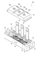
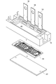
- FIG. 1 is a perspective view of a semiconductor module according to an embodiment.
- FIG. 2 is an exploded perspective view of the semiconductor module shown in FIG. 1 and shows a state where a lid is removed from the semiconductor module.
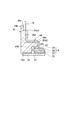
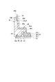
- FIG. 3 is an end view taken along line III-III in FIG.
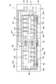
- FIG. 4 is a plan view of a semiconductor chip and a wiring board according to an embodiment.
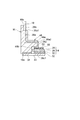
- FIG. 5 is an example of a perspective view of a frame body into which a bus bar is inserted.
- a gate pattern GP2, a source pattern SP2, and a drain pattern DP2 are provided as the wiring pattern 28.
- a MOS-FET 12a is mounted on the drain pattern DP2 so that the back surface drain electrode is electrically connected.
- the gate electrode of the MOS-FET 12a is connected to the gate pattern GP2 via a wire, and the source electrode is connected to the source pattern SP2 via another wire.
- a diode 12b is mounted on the drain pattern DP2.
- the gate pattern GP2 is electrically connected to another gate pattern G2, and the source pattern SP2 is connected to the auxiliary emitter pattern E2 and the source pattern S2 provided at one edge portion of the wiring board 14 through a wire.
- the drain pattern DP2 is connected to a drain pattern D2 provided on one edge of the wiring board 14 via a wire.
- the case 24 accommodates the wiring board 14 on which the semiconductor chip 12 is mounted therein as illustrated in FIG.
- the case 24 may include the frame body 16, the lid body 20, and the heat dissipation plate 22.
- the frame body 16 constitutes the outer peripheral wall of the case 24.
- the frame body 16 surrounds the periphery of the wiring board 14.
- the frame body 16 includes opposing side walls 36 and 38 and connecting portions 40 and 42 that connect the side walls 36 and 38 and the side walls.
- a part of the bus bar 18 is embedded in the side wall 36, and both sides thereof are inserted into the side wall 36 so as to be exposed from the side wall 36.
- an area embedded in the side wall 36 of the bus bar 18 is referred to as a first area 36a
- an area drawn from the side wall 36 on the upper opening (first opening) 16b side of the frame 16 is referred to as a first area 36a.
- the region that is drawn out from the side wall 36 to the inside of the frame 16 is referred to as a second region 36b, and is referred to as a third region 36c.
- the lid 20 can be attached to the frame 16 so as to close the upper opening of the frame 16.
- the lid 20 is formed with a hole 20a and a screw hole 20b.
- the hole 20a is formed in the lid body 20 in order to pull out the second region 36b of the bus bar 18.
- the screw hole 20b is formed in the lid body 20 in order to fix the bus bar 18 drawn out from the hole 20a and bent along the upper surface of the lid body 20 with screws.
- the lid 20 can be manufactured, for example, by molding using a thermosetting resin or a thermoplastic resin.
- the material of the lid 20 is usually the same as the material of the frame 16.
- the frame 16 in which the three bus bars 18 and the four terminals 44 are integrally inserted is prepared.
- the positions of the three bus bars 18 on the side walls 36 and an example of the manufacturing method of the frame 16 with bus bars are as described with reference to FIG.
- the third region 36c may be bent at a shallower angle at the lower corner of the rib 48 (the corner on the lower opening 16a side) than when the entire surface contacts the lower surface 48b.
- the semiconductor module 10 is mounted by attaching the lid 20 to the frame 16. Complete.
Landscapes
- Engineering & Computer Science (AREA)
- Microelectronics & Electronic Packaging (AREA)
- Physics & Mathematics (AREA)
- Condensed Matter Physics & Semiconductors (AREA)
- General Physics & Mathematics (AREA)
- Computer Hardware Design (AREA)
- Power Engineering (AREA)
- Manufacturing & Machinery (AREA)
- Cooling Or The Like Of Semiconductors Or Solid State Devices (AREA)
Abstract
一実施形態に係る半導体モジュールは、半導体チップと、配線基板と、配線基板が搭載される搭載板と、搭載板と共に、配線基板を収容するケースを構成する枠体と、配線パターンに電気的に接続されケースから引き出されるバスバーであって、枠体の一側壁にインサートされているバスバーと、を備える。一側壁は、枠体内に突出した凸部を有する。バスバーは、一側壁に埋設される第1の領域と、第1の領域の第1の端部から枠体の外側に延びている第2の領域と、第1の領域の第2の端部から枠体の内側に延びている第3の領域と、を有する。第3の領域は、第2の端部の位置からみて配線基板側の凸部の形状に基づいて屈曲されており、配線基板が搭載された搭載板が枠体に取り付けられることによって、第3の領域と配線パターンとが圧接されている。
Description
本発明は、半導体モジュール及び半導体モジュールの製造方法に関する。
半導体モジュールは、一般的に、半導体チップ、配線基板、バスバー、及び、ケースを備えている。半導体チップは、配線基板上に搭載される。配線基板には、配線パターンが形成されている。半導体チップを搭載した配線基板はケース内に収容されている。バスバーは、ケース内部の配線基板又は半導体チップからの引き出し電極として機能する。このような、半導体モジュールとしては、例えば、特許文献1,2に記載されたものが知られている。特許文献1,2記載の半導体モジュールでは、バスバーは、ケースとは別体として設けられており、バスバーの一端部を配線パターンにハンダを用いて接合されている。
上述した従来のようにハンダを利用してバスバーを配線基板に固定する場合、リフロー方式が採用される。リフロー方式ではバスバーを配線基板に垂直に固定するために固定治具などが必要であったり、ハンダ溶融時にバスバーの傾き防止をするための治具などが更に必要な場合がある。そのため、バスバーの接続工程が複雑になる場合があり得る。
したがって、本技術分野においては、容易に製造し得る半導体モジュール、及び、その製造方法が要請されている。
本発明の一側面に係る半導体モジュールは、半導体チップと、半導体チップが搭載される配線基板であって、半導体チップと電気的に接続される配線パターンが主面に形成された配線基板と、配線基板が搭載される搭載板と、搭載板と共に、配線基板を収容するケースを構成する枠体と、配線パターンに電気的に接続されケースから引き出されるバスバーであって、枠体の一側壁にインサートされているバスバーと、を備える。上記一側壁は、枠体内に突出した凸部を有する。バスバーは、上記一側壁に埋設されており、その一側壁のうち搭載板と反対側に位置する第1の端部と、凸部の先端に位置する第2の端部とを有する第1の領域と、第1の領域の第1の端部から枠体の外側に延びている第2の領域と、第1の領域の第2の端部から枠体の内側に延びている第3の領域と、を有する。第3の領域は、第2の端部の位置からみて配線基板側の凸部の形状に基づいて屈曲されており、配線基板が搭載された搭載板が枠体に取り付けられることによって、第3の領域と配線パターンとが圧接されている。
この構成では、バスバーと配線パターンとを圧接によって接続している。また、バスバーが枠体にインサートされているので、バスバーが傾いたり倒れたりすることがない。よって、半導体モジュールを容易に製造し得る。
一実施形態において、搭載板は、樹脂製の接着剤によって枠体に取り付けられていてもよい。樹脂製接着剤が硬化する際に樹脂収縮力によって、第3の領域と配線パターンとがより強く圧接され得る。
一実施形態において、搭載板は、枠体にネジ止めされていてもよい。この場合、第3の領域と配線パターンとがネジの締結力によって更に圧接され得る。
一実施形態において、第3の領域のうちの配線パターンと対向する面が粗化されていてもよい。この場合、第3の領域と、配線パターンとがより確実に接合され得る。
一実施形態において、第3の領域と対向する配線パターン上に、金属層が形成されていてよい。金属層の材料は、金、銀又は錫でありえる。この金属層に、第3の領域が食い込み易い。その結果、第3の領域と配線パターンとがより強固に接合され得る。
本発明の他の側面に係る半導体モジュールの製造方法は、(A)一側壁にバスバーがインサートされた枠体を準備する工程であって、枠体の一側壁は、前記枠体の内側に突出した凸部を有しており、バスバーは、(a)一側壁に埋設されており、一側壁のうち枠体の第1の開口側に位置する第1の端部と、凸部の先端に位置する第2の端部とを有する第1の領域と、(b)第1の領域の第1の端部から枠体の外側に延びている第2の領域と、(c)第1の領域の第2の端部から枠体の内側に延びている第3の領域と、を有し、第3の領域は、第2の端部の位置からみて第1の開口と反対側に位置する第2の開口側の凸部の形状に基づいて屈曲されている、上記準備する工程と、(B)半導体チップが搭載された配線基板が主面に搭載された搭載板を、準備された枠体の第2の開口に取り付けることによって、第3の領域と配線基板上の配線パターンとを圧接する工程と、を備える。
この製造方法では、バスバーと配線パターンとを圧接によって接続していることから、バスバーの配線パターンへの接続工程が容易である。バスバーが枠体にインサートされているので、バスバーが傾いたり倒れたりすることがない。この点においても、バスバーと配線パターンとの接続工程が容易である。よって、半導体モジュールをより容易に製造できる。
一実施形態において、準備された枠体において、凸部の第2の開口側の面と第3の領域との間に隙間を有するように、第3の領域は屈曲されていてもよい。この形態では、枠体と搭載板とが接合された場合、第3の領域が配線パターンを押圧する。そのため、第3の領域と配線パターンとがより強固に接合され得る。
一実施形態において搭載板は、枠体に樹脂製の接着剤によって取り付けられてもよい。この場合、樹脂製接着剤が硬化する際に樹脂収縮力によって、第3の領域と配線パターンとがより強く圧接され得る。
上記接着剤は、熱硬化性樹脂であり得る。熱硬化性樹脂を熱硬化させることで、上記趣旨収縮力がより大きくなる。その結果、第3の領域と配線パターンとがより強く圧接され得る。
本発明によれば、半導体モジュールをより容易に製造し得る。
以下、図面を参照して本発明の実施形態について説明する。図面の説明において、同一要素には同一符号を付し、重複する説明を省略する。図面の寸法比率は、説明のものと必ずしも一致していない。
まず、図1~図5を参照して、一実施形態に係る半導体モジュールについて説明する。図1は、一実施形態に係る半導体モジュールの斜視図である。図2は、図1に示す半導体モジュールの分解斜視図であり、半導体モジュールから蓋体を取り外した状態を示している。図3は、図2のIII-III線に沿った端面図である。図4は、一実施形態に係る半導体チップ及び配線基板の平面図である。図5は、バスバーがインサートされた枠体の斜視図の一例である。
図1~図3に示すように、半導体モジュール10は、一以上の半導体チップ12、配線基板14、枠体16、バスバー18、蓋体20及び放熱板(搭載板)22を備えている。枠体16、蓋体20及び放熱板22は、配線基板14を収容するケース24を構成する。半導体モジュール10では、半導体チップ12がケース24内部に収容されており、当該半導体チップ12と電気的に接続するバスバー18がケース24の外部に引き出されている。
図2及び図3に示すように、一以上の半導体チップ12は、配線基板14上に搭載されている。半導体チップ12としては、例えば、MOS-FET、又は、ダイオードが例示される。配線基板14は絶縁基板26を有する。絶縁基板26は、例えば、AlN、SiN、又はAl2O3といった材料から構成され得る。AlN及びSiNは、熱伝導率に優れる。Al2O3によれば、低コストの絶縁基板26を製造し得る。SiNは、Cuとの熱伝導率に近い熱伝導率を有するので、後述する放熱板22がCuから構成されている場合に、半導体モジュール10の信頼性を向上し得る。
絶縁基板26の上面(主面)には、配線パターン28が形成されている。配線パターン28の材料の例は、銅であり得る。半導体チップ12は、これら配線パターン28にワイヤ等を介して電気的に接続されている。図4は、半導体チップ12及び配線基板14のより詳細な一例を示している。図4には、半導体チップ12の例として、複数のMOS-FET 12a及び複数のダイオード12bが示されている。
一実施形態において、絶縁基板26の上面は、第1の基板領域26a及び第2の基板領域26bを含み得る。第1の基板領域26aには、配線パターン28として、ゲートパターンGP1、ソースパターンSP1、ドレインパターンDP1が設けられている。ドレインパターンDP1上には、裏面ドレイン電極が電気的に接続するように、MOS-FET 12aが搭載されている。MOS-FET 12aのゲート電極は、ワイヤを介して、ゲートパターンGP1に接続されており、ソース電極は、別のワイヤを介して、ソースパターンSP1に接続されている。ドレインパターンDP1上にはダイオード12bが搭載されている。ゲートパターンGP1は、別のゲートパターンG1に電気的に接続されており、ソースパターンSP1は、ワイヤを介して、補助エミッタパターンE1に接続されている。ドレインパターンDP1は、配線基板14の一縁部に設けられたドレインパターンD1に、ワイヤを介して接続されている。
第2の基板領域26bにも、配線パターン28として、ゲートパターンGP2、ソースパターンSP2、ドレインパターンDP2が設けられている。ドレインパターンDP2上には、裏面ドレイン電極が電気的に接続するように、MOS-FET 12aが搭載されている。MOS-FET 12aのゲート電極は、ワイヤを介して、ゲートパターンGP2に接続されており、ソース電極は、別のワイヤを介して、ソースパターンSP2に接続されている。ドレインパターンDP2上にはダイオード12bが搭載されている。ゲートパターンGP2は、別のゲートパターンG2に電気的に接続されており、ソースパターンSP2は、ワイヤを介して、補助エミッタパターンE2及び配線基板14の一縁部に設けられたソースパターンS2に接続されている。ドレインパターンDP2は、配線基板14の一縁部に設けられたドレインパターンD2に、ワイヤを介して接続されている。
絶縁基板26の下面には、放熱層30が設けられてもよい(図3参照)。放熱層30の材料の例は、銅を含む。放熱層30は、ニッケル等によってメッキされていてもよい。放熱層30の材料が、配線パターン28の材料と同じである形態では、配線基板14の反りが低減され得る。以下では、特に断らない限り、配線基板14が放熱層30を有する半導体モジュール10の実施形態について説明する。
ケース24は、図4に例示したように、半導体チップ12を搭載した配線基板14を、その内部に収容する。一実施形態においては、前述したように、ケース24は、枠体16、蓋体20、及び、放熱板22を含み得る。
放熱板22は、半導体チップ12を搭載した配線基板14をその上面(主面)上に搭載する。配線基板14が有する放熱層30が放熱板22上にハンダを利用して接合されることによって、配線基板14は放熱板22に固定される。この場合、放熱層30と放熱板22との間にハンダ層32が形成される。放熱層30と放熱板22とが接合されれば、それらを接合するための接合部材はハンダに限定されない。放熱板22は、金属板であり、放熱板22の材料の例は、Cuであり得る。
配線基板14が搭載された放熱板22は、枠体16の下部開口(第2の開口)16aを閉じるように枠体16に取り付けられる。放熱板22は、ケース24の底壁としても機能する。放熱板22は、樹脂製接着剤を利用して枠体16に接合される。従って、放熱板22と枠体16との間には、接着剤層34が形成されている。接着剤層34の材料の例は、熱硬化性樹脂であり、具体的には、エポキシ及びシリコーン系の樹脂が例示される。
枠体16は、ケース24の外周壁を構成している。枠体16は、配線基板14の周囲を囲む。枠体16は、図5に示すように、対向する側壁36,38と、側壁36,38と側壁とを連結する連結部40,42とを有する。
連結部40,42の内側には段部が形成されている。連結部40からは、外部接続用の4本の端子44,44,44,44が引き出されている。端子44~44は、それぞれゲートパターンG1、補助エミッタパターンE1、補助エミッタパターンE2及びゲートパターンG2に電気的に接続され得る。これらの電気的接続は、例えば、連結部40の段部に、各端子44に電気的にそれぞれ接続された電極46と、ゲートパターンG1、補助エミッタパターンE1、補助エミッタパターンE2及びゲートパターンG2とをワイヤによって接続すればよい。図2では、ゲートパターンG1,G2と端子44,44とが電気的に接続され得る電極46を例示している。
側壁(一側壁)36は、その内側に、枠体16内に突出したリブ(凸部)48を有する。従って、側壁36は、枠体16の下部開口16a側(放熱板22の取付け側)から見た場合、オーバーハング部を有する。リブ48は、ケース24の深さ方向(絶縁基板26の法線方向)に直交する方向(図2,5において、枠体16の長手方向)に延在している。リブ48の延在方向に直交する断面の外形形状は、図3に例示するように、U字状であり得る。
リブ48が形成された側壁36に3本のバスバー18が一体的にインサートされている。
バスバー18は、ケース24からの引き出し電極として機能する。バスバー18は、一枚の導電性を有する金属板であり得る。3本のバスバー18は、枠体16に放熱板22が取り付けられた状態において、ドレインパターンD1,ソースパターンS2及びドレインパターンD2(図4参照)の位置に対応して側壁36にそれぞれ設けられている。
バスバー18は、図3に示すように、一部が側壁36に埋設され、その両側が側壁36から露出するように側壁36にインサートされている。以下の説明では、バスバー18のうち側壁36内に埋設されている領域を第1の領域36aと称し、枠体16の上部開口(第1の開口)16b側において側壁36から引き出された領域を第2の領域36bと称し、側壁36から枠体16の内側に引き出された領域を第3の領域36cと称す。
第1の領域36aは、側壁36の上端部とリブ48の先端部48aとを繋ぐように屈曲している。具体的には、第1の領域36aは、側壁36の上端部側から枠体16の深さ方向に平行に延びた後、リブ48の位置で絶縁基板26の上面と平行に折り曲げられ、リブ48の先端48aまで延びている。第1の領域36aは、第1の領域36aを側方からみた場合(3本のバスバー18の配列方向から見た場合)、図3に示すように、L字状であり得る。第1の領域36aにおいて、上部開口16b側を第1の端部36a1と称し、リブ48の先端48a側の部分を第2の端部36a2と称す。第1の領域36aは、第2の領域36bと第3の領域36cとを繋いでいる。
第2の領域36bは、第1の領域36aの第1の端部36a1から枠体16の外側に延びている。従って、第2の領域36bにおいて、第1の端部36a1と反対側の端部は、枠体16の外側に位置する。
第3の領域36cは、第1の領域36aの第2の端部36a2から枠体16の内側に延びている。第3の領域36cは、リブ48において下部開口16a側の形状に沿って曲げられている。すなわち、第3の領域36cは、第2の端部36a2から下側に向けて枠体16の深さ方向に平行に延びた後、リブ48の下側角部で屈曲してリブ48の下面48b側に向けて折り曲げられている。
半導体モジュール10では、第3の領域36cのうちリブ48の下面48bに被さっている部分と配線パターン28とが圧接されている。具体的には、3本のバスバー18,18,18それぞれの第3の領域36aと、各バスバー18,18,18に対応するドレインパターンD1,ソースパターンS2及びドレインパターンD2とが圧接されている。リブ48の位置は、放熱板22を枠体16に取り付けた際に、第3の領域36cと配線パターン28とが接触するように、調節されている。
一実施形態において、図6に示すように、第3の領域36cにおいて、配線パターン28と対向する面(以下、対向面と称す)36c1は、粗化された面(以下、粗面と称す)でもよい。粗面の例は、梨地面である。粗面は、例えば、ブラスト処理又はレーザ加工といった物理的処理や、エッチングといった化学的処理によって形成され得る。
一実施形態において、図6に示すように、配線パターン28のうち第3の領域36cと対向する部分(図6では、ソースパターンS2)には、配線パターン28より柔らかい金属から構成される金属層50が形成されていてもよい。金属層50の材料の例は、金、銀及び錫を含む。このような金属層50は、配線パターン28のうち第3の領域36cと対向する部分を、金、銀又は錫によってメッキすることによって形成され得る。
バスバー18が一体成形された枠体16は、例えば、熱硬化性樹脂又は熱可塑性樹脂を用いた成形によって製造され得る。バスバー18が一体的にインサートされた枠体16の成形技術の例は、射出成形である。
蓋体20は、枠体16の上部開口を閉じるように枠体16に取り付けられ得る。この蓋体20には、孔20a、及びネジ孔20bが形成されている。孔20aは、バスバー18の第2の領域36bを引き出すために蓋体20に形成されている。ネジ孔20bは、孔20aから引き出され蓋体20の上面に沿うように折り曲げられたバスバー18を、ネジによって固定するために、当該蓋体20に形成されている。蓋体20は、例えば、熱硬化性樹脂又は熱可塑性樹脂を用いた成形により製造され得る。蓋体20の材料は、通常、枠体16の材料と同じである。
次に、半導体モジュール10の製造方法の一例について説明する。まず、図5に示したように、3本のバスバー18及び4本の端子44が一体的にインサートされた枠体16を準備する。3本のバスバー18の側壁36における位置及びバスバー付の枠体16の製造方法の例などは、図3を利用して説明した通りである。
一実施形態において、バスバー付きの枠体16を準備する場合には、図7に示したように、バスバー18の第3の領域36cとリブ48の下面48bとの間に隙間が生じていてもよい。換言すれば、リブ48の下側角部(下部開口16a側の角部)において、第3の領域36cは、下面48bに全面が接触するよりも浅い角度で折り曲げられていてもよい。
続く工程において、図8に示すように、半導体チップ12を搭載した配線基板14を放熱板22上に搭載する。その後、配線基板14が搭載された放熱板22を枠体16に樹脂製接着剤を介して接合すると共に、放熱板22を枠体16に圧接する。これにより、3本のバスバー18と、配線パターン28(具体的に、ドレインパターンD1、ソースパターンS2及びドレインパターンD2)とが圧接される。その結果、それらが電気的に接続される。樹脂製接着剤が熱硬化樹脂である場合には、樹脂性接着剤を更に熱硬化させる。
その後の工程において、端子44,44と、ゲートパターンG1及びゲートパターンG2とをワイヤによって接続する等の所定の配線を行った後、蓋体20を枠体16に取り付けることによって、半導体モジュール10が完成する。
以上説明した種々の実施形態の半導体モジュール10及びその製造方法によれば、バスバー18が枠体16にインサート成形されているので、枠体16とバスバー18とが一体化している。そのため、バスバー18が傾いたり倒れたりすることがないので、バスバー18と配線パターン28との電気的接触を形成する場合に、バスバー18を固定する等の治具が不要である。従って、治具などを準備する手間が省けると共に、製造コストの低減を図り得る。
バスバー18と配線パターン28とをハンダといった接続部材を利用せずに、圧接によって接続していることから、バスバー18の配線パターン28への接続工程が容易である。更に、上記半導体モジュール10及びその製造方法では、ハンダを利用する場合に必要なハンダペースト塗布やリフロー工程が不要である。従って、半導体モジュール10の製造が容易である。
更に、電力用に使用される半導体モジュールでは、仮に、バスバーと配線パターンとをハンダを利用して接続していると、半導体モジュールを使用した時のヒートサイクルに起因してバスバーと配線パターンとの間のハンダ層に亀裂が入る場合がある。その結果、半導体モジュールの信頼性が低下する傾向にある。しかしながら、半導体モジュール10では、バスバー18と配線パターン28とを圧接により接合しているので、ハンダを利用している場合に比べて信頼性が向上し得る。
樹脂製接着剤を利用して放熱板22を枠体16に接合する場合、樹脂製接着剤が硬化する際の樹脂収縮力によって、第3の領域36cと配線パターン28とがより強く圧接される。これにより、第3の領域36cと配線パターン28とが強固に接合され得る。樹脂製接着剤が熱硬化性樹脂である場合、熱硬化によって更に樹脂収縮力が高まるので、第3の領域36cと配線パターン28との接合力が高まる。
更に、図6を利用して説明した形態のように、第3の領域36cにおける、配線パターン28との対向面36c1が粗面である形態では、第3の領域36cと、配線パターン28とがずれにくいと共に、それらの接触面積が実質的に向上する。そのため、第3の領域36cと配線パターン28とがより確実に接合され得る。
図6を利用して説明した形態のように、配線パターン28上に金属層50が形成されている場合、金属層50は配線パターン28より柔らかいので、第3の領域36cが金属層50に食い込み易い。その結果、第3の領域36cと配線パターン28とがより強固に接合され得る。
図7に示したように、枠体16にインサートされたバスバー18の第3の領域36cと下面48bとの間に隙間がある形態では、枠体16と放熱板22とが接合された場合、第3の領域36cは配線パターン28によって、リブ48と第3の領域36cとの隙間をうめるように更に曲げられる。その反作用によって、第3の領域36cが配線パターン28を押圧する。そのため、第3の領域36cと配線パターン28とがより強固に接合され得る。
以上、本発明の種々の実施形態について説明したが、本発明は、これまで説明した実施形態に限定されるものではなく、発明の趣旨を逸脱しない範囲で種々の変更が可能である。例えば、図9に示すように、放熱板22と枠体16との接合部において、ネジ孔52を形成して、放熱板22を枠体16にネジ止めしてもよい。この形態では、第3の領域36cと配線パターン28とがネジ54の締結力によっても圧接される。そのため、第3の領域36cと配線パターン28とがより強固に接合され得る。ネジ54は、例えば、放熱板22の表面から枠体16に向かって0.5mm程度入っていればよい。
図6では、対向面36c1が粗面である形態と、金属層50を備える形態とを合わせて図示しているが、対向面36c1が粗面であっても金属層50を備え無くてもよい。逆に、金属層50が、第3の領域36cと対向する配線パターン28上に設けられていても、対向面36c1は平坦な面でもよい。
種々の実施形態では、バスバー18の本数などを例示して説明したが、バスバー18の数などは、例示した種々の実施形態の数に限定されない。搭載板として放熱板を例示したが、配線基板が搭載される板であればよい。
これまで例示した種々の実施形態が互いに組み合わされてもよい。
10…半導体モジュール、12…半導体チップ、14…配線基板、16…枠体、16a…下部開口(第2の開口)、16b…上部開口(第1の開口)、18…バスバー、22…放熱板(搭載板)、24…ケース、26…絶縁基板、28…配線パターン、36…一側壁、36a…第1の領域、36a1…第1の端部、36a2…第2の端部、36b…第2の領域、36c…第3の領域、36c1…対向面(配線パターンと対向する面)、48…リブ(凸部)、48a…先端、48b…下面(凸部の第2の開口側又は搭載板側の面)、50…金属層、52…ネジ。
Claims (9)
- 半導体チップと、
前記半導体チップが搭載される配線基板であって、前記半導体チップと電気的に接続される配線パターンが主面に形成された前記配線基板と、
前記配線基板が搭載される搭載板と、
前記搭載板と共に、前記配線基板を収容するケースを構成する枠体と、
前記配線パターンに電気的に接続され前記ケースから引き出されるバスバーであって、前記枠体の一側壁にインサートされている前記バスバーと、
を備え、
前記一側壁は、前記枠体内に突出した凸部を有し、
前記バスバーは、
前記一側壁に埋設されており、前記一側壁のうち前記搭載板と反対側に位置する第1の端部と、前記凸部の先端に位置する第2の端部とを有する第1の領域と、
前記第1の領域の前記第1の端部から前記枠体の外側に延びている第2の領域と、
前記第1の領域の前記第2の端部から前記枠体の内側に延びている第3の領域と、
を有し、
前記第3の領域は、前記第2の端部の位置からみて前記配線基板側の前記凸部の形状に基づいて屈曲されており、
前記配線基板が搭載された前記搭載板が前記枠体に取り付けられることによって、前記第3の領域と前記配線パターンとが圧接されている、
半導体モジュール。 - 前記搭載板は、樹脂製の接着剤によって前記枠体に取り付けられている、
請求項1記載の半導体モジュール。 - 前記搭載板は、前記枠体にネジ止めされている、
請求項2記載の半導体モジュール。 - 前記第3の領域のうちの前記配線パターンと対向する面が粗化されている、
請求項1~3の何れか一項記載の半導体モジュール。 - 前記第3の領域と対向する前記配線パターン上に、金属層が形成されており、
前記金属層の材料は、金、銀又は錫である、
請求項1~4の何れか一項記載の半導体モジュール。 - 一側壁にバスバーがインサートされた枠体を準備する工程であって、
前記枠体の一側壁は、前記枠体の内側に突出した凸部を有しており、
前記バスバーは、
前記一側壁に埋設されており、前記一側壁のうち前記枠体の第1の開口側に位置する第1の端部と、前記凸部の先端に位置する第2の端部とを有する第1の領域と、
前記第1の領域の前記第1の端部から前記枠体の外側に延びている第2の領域と、
前記第1の領域の前記第2の端部から前記枠体の内側に延びている第3の領域と、
を有し、
前記第3の領域は、前記第2の端部の位置からみて前記第1の開口と反対側に位置する第2の開口側の前記凸部の形状に基づいて屈曲されている、
前記準備する工程と、
半導体チップが搭載された配線基板が主面に搭載された搭載板を、準備された前記枠体の前記第2の開口に取り付けることによって、前記第3の領域と前記配線基板上の配線パターンとを圧接する工程と、
を備える、半導体モジュールの製造方法。 - 準備された前記枠体において、前記凸部の前記第2の開口側の面と前記第3の領域との間に隙間を有するように、前記第3の領域は屈曲されている、
請求項6記載の半導体モジュールの製造方法。 - 前記搭載板は、前記枠体に樹脂製の接着剤によって取り付けられている、
請求項6又は7記載の半導体モジュールの製造方法。 - 前記接着剤が熱硬化性樹脂である、請求項8記載の半導体モジュールの製造方法。
Priority Applications (2)
| Application Number | Priority Date | Filing Date | Title |
|---|---|---|---|
| CN201380028644.5A CN104350594B (zh) | 2012-06-01 | 2013-05-13 | 半导体模块和半导体模块制造方法 |
| EP13796387.2A EP2858109B1 (en) | 2012-06-01 | 2013-05-13 | Semiconductor module and semiconductor module manufacturing method |
Applications Claiming Priority (2)
| Application Number | Priority Date | Filing Date | Title |
|---|---|---|---|
| JP2012-125822 | 2012-06-01 | ||
| JP2012125822A JP5939041B2 (ja) | 2012-06-01 | 2012-06-01 | 半導体モジュール及び半導体モジュールの製造方法 |
Publications (1)
| Publication Number | Publication Date |
|---|---|
| WO2013179879A1 true WO2013179879A1 (ja) | 2013-12-05 |
Family
ID=49670004
Family Applications (1)
| Application Number | Title | Priority Date | Filing Date |
|---|---|---|---|
| PCT/JP2013/063290 WO2013179879A1 (ja) | 2012-06-01 | 2013-05-13 | 半導体モジュール及び半導体モジュールの製造方法 |
Country Status (5)
| Country | Link |
|---|---|
| US (1) | US9263381B2 (ja) |
| EP (1) | EP2858109B1 (ja) |
| JP (1) | JP5939041B2 (ja) |
| CN (1) | CN104350594B (ja) |
| WO (1) | WO2013179879A1 (ja) |
Families Citing this family (13)
| Publication number | Priority date | Publication date | Assignee | Title |
|---|---|---|---|---|
| CN105190882B (zh) * | 2013-03-21 | 2018-04-03 | 三菱电机株式会社 | 半导体装置 |
| JP6299120B2 (ja) * | 2013-09-05 | 2018-03-28 | 富士電機株式会社 | 半導体モジュール |
| JP6323325B2 (ja) * | 2014-04-21 | 2018-05-16 | 三菱電機株式会社 | 半導体装置、半導体装置の製造方法 |
| US10564316B2 (en) | 2014-09-12 | 2020-02-18 | The Climate Corporation | Forecasting national crop yield during the growing season |
| JP6272213B2 (ja) * | 2014-11-26 | 2018-01-31 | 三菱電機株式会社 | 半導体装置 |
| JP6645134B2 (ja) * | 2015-11-16 | 2020-02-12 | 富士電機株式会社 | 半導体装置および半導体装置の製造方法 |
| JP6607077B2 (ja) * | 2016-02-23 | 2019-11-20 | 三菱電機株式会社 | 半導体装置 |
| JP6567996B2 (ja) * | 2016-03-11 | 2019-08-28 | 京セラ株式会社 | パワー半導体モジュール |
| US10398096B2 (en) | 2016-11-16 | 2019-09-03 | The Climate Corporation | Identifying management zones in agricultural fields and generating planting plans for the zones |
| US10028451B2 (en) | 2016-11-16 | 2018-07-24 | The Climate Corporation | Identifying management zones in agricultural fields and generating planting plans for the zones |
| JP6415676B1 (ja) * | 2017-12-07 | 2018-10-31 | 株式会社三社電機製作所 | 半導体モジュール |
| KR102152014B1 (ko) | 2020-03-03 | 2020-09-04 | 제엠제코(주) | 가압형 반도체 패키지 및 이의 제조방법 |
| CN112885241B (zh) * | 2021-02-07 | 2022-12-02 | 业成科技(成都)有限公司 | 框架及其制造方法、显示模组及其测量方法与电子设备 |
Citations (5)
| Publication number | Priority date | Publication date | Assignee | Title |
|---|---|---|---|---|
| JPS63240056A (ja) * | 1986-12-18 | 1988-10-05 | セミクロン エレクトロニク ゲーエムベーハー | 半導体組立ユニット |
| JPH11251514A (ja) | 1998-03-05 | 1999-09-17 | Sansha Electric Mfg Co Ltd | 電力用半導体モジュール |
| JP2001135762A (ja) * | 1999-11-10 | 2001-05-18 | Nissan Motor Co Ltd | 半導体素子の実装構造 |
| JP2006344841A (ja) | 2005-06-10 | 2006-12-21 | Mitsubishi Electric Corp | パワー半導体モジュール |
| WO2009069308A1 (ja) * | 2007-11-30 | 2009-06-04 | Panasonic Corporation | 放熱構造体基板とこれを用いたモジュール及び放熱構造体基板の製造方法 |
Family Cites Families (16)
| Publication number | Priority date | Publication date | Assignee | Title |
|---|---|---|---|---|
| JP3519300B2 (ja) * | 1999-01-11 | 2004-04-12 | 富士電機デバイステクノロジー株式会社 | パワーモジュールのパッケージ構造 |
| DE69937739T2 (de) * | 1999-05-11 | 2008-11-27 | Mitsubishi Denki K.K. | Halbleitervorrichtung |
| JP4218193B2 (ja) * | 2000-08-24 | 2009-02-04 | 三菱電機株式会社 | パワーモジュール |
| JP2003264265A (ja) * | 2002-03-08 | 2003-09-19 | Mitsubishi Electric Corp | 電力用半導体装置 |
| US6933593B2 (en) * | 2003-08-14 | 2005-08-23 | International Rectifier Corporation | Power module having a heat sink |
| JP2006186170A (ja) * | 2004-12-28 | 2006-07-13 | Nissan Motor Co Ltd | 半導体装置 |
| JP4731418B2 (ja) * | 2006-07-10 | 2011-07-27 | 三菱電機株式会社 | 半導体モジュール |
| JP2008252054A (ja) * | 2007-03-06 | 2008-10-16 | Matsushita Electric Ind Co Ltd | 半導体装置および半導体装置の製造方法 |
| JP5166943B2 (ja) * | 2008-04-03 | 2013-03-21 | 矢崎総業株式会社 | バスバーの組付構造 |
| JP5341587B2 (ja) * | 2009-03-23 | 2013-11-13 | 矢崎総業株式会社 | バスバ装置及びヒュージブルリンクユニット |
| JP5611537B2 (ja) * | 2009-04-28 | 2014-10-22 | 日立化成株式会社 | 導電性接合材料、それを用いた接合方法、並びにそれによって接合された半導体装置 |
| JP5617278B2 (ja) * | 2010-02-26 | 2014-11-05 | 株式会社デンソー | 電流検出装置 |
| WO2011149017A1 (ja) * | 2010-05-27 | 2011-12-01 | 京セラ株式会社 | 半導体モジュール基板および半導体モジュール |
| CN102438426B (zh) * | 2010-08-20 | 2016-08-24 | 住友电气工业株式会社 | 具有从tosa到金属壳体的有效传热路径的光收发器 |
| JP5533431B2 (ja) * | 2010-08-23 | 2014-06-25 | 住友電気工業株式会社 | 光モジュール |
| CN103370788B (zh) * | 2011-04-01 | 2016-10-12 | 富士电机株式会社 | 半导体装置及其制造方法 |
-
2012
- 2012-06-01 JP JP2012125822A patent/JP5939041B2/ja active Active
-
2013
- 2013-05-13 CN CN201380028644.5A patent/CN104350594B/zh active Active
- 2013-05-13 EP EP13796387.2A patent/EP2858109B1/en active Active
- 2013-05-13 WO PCT/JP2013/063290 patent/WO2013179879A1/ja active Application Filing
- 2013-05-23 US US13/901,173 patent/US9263381B2/en active Active
Patent Citations (5)
| Publication number | Priority date | Publication date | Assignee | Title |
|---|---|---|---|---|
| JPS63240056A (ja) * | 1986-12-18 | 1988-10-05 | セミクロン エレクトロニク ゲーエムベーハー | 半導体組立ユニット |
| JPH11251514A (ja) | 1998-03-05 | 1999-09-17 | Sansha Electric Mfg Co Ltd | 電力用半導体モジュール |
| JP2001135762A (ja) * | 1999-11-10 | 2001-05-18 | Nissan Motor Co Ltd | 半導体素子の実装構造 |
| JP2006344841A (ja) | 2005-06-10 | 2006-12-21 | Mitsubishi Electric Corp | パワー半導体モジュール |
| WO2009069308A1 (ja) * | 2007-11-30 | 2009-06-04 | Panasonic Corporation | 放熱構造体基板とこれを用いたモジュール及び放熱構造体基板の製造方法 |
Non-Patent Citations (1)
| Title |
|---|
| See also references of EP2858109A4 |
Also Published As
| Publication number | Publication date |
|---|---|
| US9263381B2 (en) | 2016-02-16 |
| JP2013251429A (ja) | 2013-12-12 |
| CN104350594A (zh) | 2015-02-11 |
| EP2858109A4 (en) | 2015-08-19 |
| EP2858109B1 (en) | 2016-08-03 |
| CN104350594B (zh) | 2017-05-10 |
| EP2858109A1 (en) | 2015-04-08 |
| JP5939041B2 (ja) | 2016-06-22 |
| US20130322025A1 (en) | 2013-12-05 |
Similar Documents
| Publication | Publication Date | Title |
|---|---|---|
| JP5939041B2 (ja) | 半導体モジュール及び半導体モジュールの製造方法 | |
| JP5252819B2 (ja) | 半導体装置およびその製造方法 | |
| JP6044321B2 (ja) | 半導体モジュール | |
| JP6132034B2 (ja) | 半導体モジュール | |
| US7919854B2 (en) | Semiconductor module with two cooling surfaces and method | |
| CN104485321A (zh) | 半导体管芯封装件及其制造方法 | |
| JP5071405B2 (ja) | 電力用半導体装置 | |
| JP4570092B2 (ja) | 半導体モジュール | |
| JP5935374B2 (ja) | 半導体モジュールの製造方法 | |
| JP2005340639A (ja) | 半導体装置及び三相インバータ装置 | |
| CN112750801B (zh) | 功率半导体装置 | |
| KR100575216B1 (ko) | 발광소자용 패캐지 베이스 | |
| JP2005191146A (ja) | 混成集積回路装置の製造方法 | |
| JP2013033874A (ja) | パワーモジュール | |
| JP3169578B2 (ja) | 電子部品用基板 | |
| WO2022004332A1 (ja) | 回路構成体 | |
| JP2009158769A (ja) | 半導体装置 | |
| JP2012216654A (ja) | 樹脂成形フレーム及び光半導体装置 | |
| KR20140135443A (ko) | 반도체 모듈의 제조 방법 및 이에 따른 반도체 모듈 | |
| US20120146208A1 (en) | Semiconductor module and manufacturing method thereof | |
| JP2006203977A (ja) | 電気接続箱 | |
| KR20160051513A (ko) | 전력 모듈 및 그 제조 방법 | |
| JP2003007379A (ja) | フラット電線の接続構造および接続方法 | |
| KR102551746B1 (ko) | 광원모듈 | |
| JP2012099773A (ja) | 半導体モジュールの製造方法、及び半導体モジュール |
Legal Events
| Date | Code | Title | Description |
|---|---|---|---|
| 121 | Ep: the epo has been informed by wipo that ep was designated in this application |
Ref document number: 13796387 Country of ref document: EP Kind code of ref document: A1 |
|
| REEP | Request for entry into the european phase |
Ref document number: 2013796387 Country of ref document: EP |
|
| WWE | Wipo information: entry into national phase |
Ref document number: 2013796387 Country of ref document: EP |
|
| NENP | Non-entry into the national phase |
Ref country code: DE |